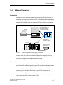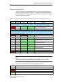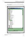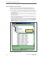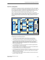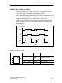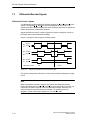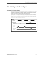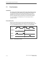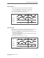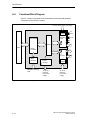
1
Preface, Contents SIMATIC Product Overview Getting Started FM 352-5 High-Speed Boolean Processor Installing and Removing the FM 352-5 Wiring the FM 352-5 User Manual Configuring the FM 352-5 1 2 3 4 5 Programming and Operating the FM 352-5 6 Encoder Signals and their Evaluation 7 Diagnostics and Troubleshooting Using the FM 352-5 with Non-S7 Masters 8 9 Appendices Specifications A Parts Lists B Index Edition 04/2003 A5E00131318-03 Safety Guidelines This manual contains notices intended to ensure personal safety, as well as to protect the products and connected equipment against damage. These notices are highlighted by the symbols shown below and graded according to severity by the following texts: ! ! ! Danger indicates that death, severe personal injury or substantial property damage will result if proper precautions are not taken. Warning indicates that death, severe personal injury or substantial property damage can result if proper precautions are not taken. Caution indicates that minor personal injury can result if proper precautions are not taken. Caution indicates that property damage can result if proper precautions are not taken. Notice draws your attention to particularly important information on the product, handling the product, or to a particular part of the documentation. Qualified Personnel Only qualified personnel should be allowed to install and work on this equipment. Qualified persons are defined as persons who are authorized to commission, to ground and to tag circuits, equipment, and systems in accordance with established safety practices and standards. Correct Usage Note the following: ! Warning This device and its components may only be used for the applications described in the catalog or the technical description, and only in connection with devices or components from other manufacturers which have been approved or recommended by Siemens. This product can only function correctly and safely if it is transported, stored, set up, and installed correctly, and operated and maintained as recommended. Trademarks SIMATIC, SIMATIC HMI and SIMATIC NET are registered trademarks of SIEMENS AG. Third parties using for their own purposes any other names in this document which refer to trademarks might infringe upon the rights of the trademark owners. Copyright W Siemens AG 2003 All rights reserved Disclaim of Liability The reproduction, transmission or use of this document or its contents is not permitted without express written authority. Offenders will be liable for damages. All rights, including rights created by patent grant or registration of a utility model or design, are reserved. We have checked the contents of this manual for agreement with the hardware and software described. Since deviations cannot be precluded entirely, we cannot guarantee full agreement. However, the data in this manual are reviewed regularly and any necessary corrections included in subsequent editions. Suggestions for improvement are welcomed. Siemens Energy & Automation, Inc. 3333 Old Milton Parkway Alpharetta, GA 30202 Index-2Aktiengesellschaft Siemens Siemens AG 2003 Technical data subject to change. FM 352-5 High-Speed Boolean Processor A5E00131318-03 A5E000131318-03 Preface Purpose of the Manual This manual describes the purpose, features, and operating functions of the SIMATIC S7 FM 352-5 High-Speed Boolean Processor Modules (MLFB: 6ES7352-5AH00-0AE0) and (MLFB: 6ES7352-5AH10–0AE0). This manual also enables you to install, configure, program, and operate the FM 352-5 modules. Contents of the Manual This manual describes the FM 352-5 hardware and the software required to configure and program the modules. It consists of chapters containing instructions and reference chapters (technical specifications). This manual deals with the following topics: • Installing and wiring the FM 352-5 modules • Configuring the FM 352-5 modules • Assigning operating mode parameters to the FM 352-5 modules • Programming the FM 352-5 modules • Operating the modules • Troubleshooting and diagnostics Related Documentation Consult the documentation for the SIMATIC S7-300 Programmable Controller system and the STEP 7 programming software for complete information on installing and programming the FM 352-5 High-Speed Boolean Processor Modules. CD-ROM The entire SIMATIC Manual Collection is also available on CD-ROM. FM 352-5 High-Speed Boolean Processor A5E00131318-03 iii Preface Standards, Certificates, and Approvals The FM 352-5 fulfills the requirements and criteria of IEC 1131, Part 2, and the requirements for obtaining the CE marking. The following agency approvals apply: FM Class I, Div 2, Group A, B, C, D and cULus Class I, Div 2 Group A, B, C, D. Please refer to Section A.1 for further details on standards, certificates, and approvals. Aids to Finding Information You can access specific information in the manual by using the following aids: • At the beginning of the manual you will find a comprehensive table of contents and lists of the figures and tables contained in the manual. • In the different chapters you will find subheadings that allow you to gain an overview of what is contained in each section. • At the end of the manual you will find a comprehensive index enabling rapid access to the information you are looking for. Technical Support If you have questions concerning the information on the FM 352-5 modules contained in this manual, contact your Siemens Energy & Automation, Inc., distributor or sales office. If you require assistance in contacting your distributor or sales office in the United States, phone 1–800-964-4114. For additional technical assistance, call the Siemens Technical Services Group in Johnson City, Tennessee at 423-461-2522, or contact them by e-mail at [email protected] . For technical assistance outside the United States, call +49-911-895-7000. Constantly Updated Information You can obtain constantly updated information on the SIMATIC products on the Internet at http://www.ad.siemens.de. In addition, SIMATIC Customer Support provides you with up-to-date information and downloads that can be useful to you when using SIMATIC products: • On the Internet at http://www4.ad.siemens.de/csinfo/livelink.exe • By means of the SIMATIC Customer Support Mailbox at +49-911-895-7100 To dial the mailbox, use a modem capable of up to V.34 (28.8 kbps) and set its parameters as follows: 8, N, 1, ANSI. Alternatively, dial in using ISDN (x.75, 64 kbps). You can contact SIMATIC Customer Support at +49-911-895-7000 or by fax at +49-911-895-7002. You can also send e-mail or send a message to the above mailbox. iv FM 352-5 High-Speed Boolean Processor A5E00131318-03 Contents 1 2 3 4 5 Product Overview . . . . . . . . . . . . . . . . . . . . . . . . . . . . . . . . . . . . . . . . . . . . . . . . . . . . . . 1-1 1.1 Functions of the FM 352-5 Module . . . . . . . . . . . . . . . . . . . . . . . . . . . . . . . . . 1-2 1.2 Physical Features of the Module . . . . . . . . . . . . . . . . . . . . . . . . . . . . . . . . . . . 1-4 1.3 System Configurations . . . . . . . . . . . . . . . . . . . . . . . . . . . . . . . . . . . . . . . . . . . 1-6 1.4 Modes of Operation . . . . . . . . . . . . . . . . . . . . . . . . . . . . . . . . . . . . . . . . . . . . . 1-7 1.5 Overview of Basic Tasks . . . . . . . . . . . . . . . . . . . . . . . . . . . . . . . . . . . . . . . . . 1-8 Getting Started . . . . . . . . . . . . . . . . . . . . . . . . . . . . . . . . . . . . . . . . . . . . . . . . . . . . . . . . . 2-1 2.1 Overview . . . . . . . . . . . . . . . . . . . . . . . . . . . . . . . . . . . . . . . . . . . . . . . . . . . . . . . 2-2 2.2 Running the FM 352-5 Example Program . . . . . . . . . . . . . . . . . . . . . . . . . . . 2-3 Installing and Removing the FM 352-5 . . . . . . . . . . . . . . . . . . . . . . . . . . . . . . . . . . . 3-1 3.1 Installation Rules . . . . . . . . . . . . . . . . . . . . . . . . . . . . . . . . . . . . . . . . . . . . . . . . 3-2 3.2 Installation in an S7-300 System . . . . . . . . . . . . . . . . . . . . . . . . . . . . . . . . . . 3-3 3.3 Installation in a Stand-Alone System . . . . . . . . . . . . . . . . . . . . . . . . . . . . . . . 3-4 Wiring the FM 352-5 . . . . . . . . . . . . . . . . . . . . . . . . . . . . . . . . . . . . . . . . . . . . . . . . . . . . 4-1 4.1 General Rules and Regulations . . . . . . . . . . . . . . . . . . . . . . . . . . . . . . . . . . . 4-2 4.2 Terminal Assignments of the Front Connector . . . . . . . . . . . . . . . . . . . . . . . 4-4 4.3 Wiring the Module . . . . . . . . . . . . . . . . . . . . . . . . . . . . . . . . . . . . . . . . . . . . . . . 4-8 4.4 Connecting Encoder Cables . . . . . . . . . . . . . . . . . . . . . . . . . . . . . . . . . . . . . . 4-9 4.5 Connecting Shielded Cables via a Shield Contact Element . . . . . . . . . . . . 4-11 Configuring the FM 352-5 . . . . . . . . . . . . . . . . . . . . . . . . . . . . . . . . . . . . . . . . . . . . . . . 5-1 5.1 Installing the Configuration/Programming Software . . . . . . . . . . . . . . . . . . . 5-2 5.2 Basic Tasks at a Glance . . . . . . . . . . . . . . . . . . . . . . . . . . . . . . . . . . . . . . . . . . 5-4 5.3 Checking the Consistency of Program and Configuration . . . . . . . . . . . . . 5-5 5.4 Overview of Hardware Configuration . . . . . . . . . . . . . . . . . . . . . . . . . . . . . . . 5-6 5.5 Setting Up the Hardware Configuration . . . . . . . . . . . . . . . . . . . . . . . . . . . . . 5-7 5.6 Assigning Properties and Parameters . . . . . . . . . . . . . . . . . . . . . . . . . . . . . . 5-9 5.7 Selecting Input Filters . . . . . . . . . . . . . . . . . . . . . . . . . . . . . . . . . . . . . . . . . . . . 5-15 5.8 Saving and Compiling the Hardware Configuration . . . . . . . . . . . . . . . . . . . 5-17 5.9 Programming Control . . . . . . . . . . . . . . . . . . . . . . . . . . . . . . . . . . . . . . . . . . . . 5-18 FM 352-5 High-Speed Boolean Processor A5E00131318-03 v Contents 6 7 8 9 A vi Programming and Operating the FM 352-5 . . . . . . . . . . . . . . . . . . . . . . . . . . . . . . . . 6-1 6.1 Overview . . . . . . . . . . . . . . . . . . . . . . . . . . . . . . . . . . . . . . . . . . . . . . . . . . . . . . . 6-2 6.2 Creating the Application Function Block . . . . . . . . . . . . . . . . . . . . . . . . . . . . 6-3 6.3 Setting up the Interface FB/DB Set . . . . . . . . . . . . . . . . . . . . . . . . . . . . . . . . 6-29 6.4 Debugging the Program . . . . . . . . . . . . . . . . . . . . . . . . . . . . . . . . . . . . . . . . . . 6-37 6.5 Downloading the Program to the FM 352-5 . . . . . . . . . . . . . . . . . . . . . . . . . 6-38 6.6 Stand-alone Operation . . . . . . . . . . . . . . . . . . . . . . . . . . . . . . . . . . . . . . . . . . . 6-40 6.7 Controlling Dynamic Parameters . . . . . . . . . . . . . . . . . . . . . . . . . . . . . . . . . . 6-41 6.8 Memory Operations . . . . . . . . . . . . . . . . . . . . . . . . . . . . . . . . . . . . . . . . . . . . . 6-42 6.9 Instruction Set for Ladder Logic Programming . . . . . . . . . . . . . . . . . . . . . . . 6-43 Encoder Signals and their Evaluation . . . . . . . . . . . . . . . . . . . . . . . . . . . . . . . . . . . . 7-1 7.1 Types of Encoders . . . . . . . . . . . . . . . . . . . . . . . . . . . . . . . . . . . . . . . . . . . . . . 7-2 7.2 Counting Modes for the Incremental Encoders . . . . . . . . . . . . . . . . . . . . . . 7-5 7.3 Differential Encoder Signals . . . . . . . . . . . . . . . . . . . . . . . . . . . . . . . . . . . . . . . 7-10 7.4 24 V Single-ended Encoder Signals . . . . . . . . . . . . . . . . . . . . . . . . . . . . . . . . 7-11 7.5 Pulse Evaluation . . . . . . . . . . . . . . . . . . . . . . . . . . . . . . . . . . . . . . . . . . . . . . . . 7-12 7.6 SSI Absolute Encoders . . . . . . . . . . . . . . . . . . . . . . . . . . . . . . . . . . . . . . . . . . 7-15 Diagnostics and Troubleshooting . . . . . . . . . . . . . . . . . . . . . . . . . . . . . . . . . . . . . . . . 8-1 8.1 Reading the Status LEDs . . . . . . . . . . . . . . . . . . . . . . . . . . . . . . . . . . . . . . . . . 8-2 8.2 Diagnostic Messages . . . . . . . . . . . . . . . . . . . . . . . . . . . . . . . . . . . . . . . . . . . . 8-3 8.3 Interrupts . . . . . . . . . . . . . . . . . . . . . . . . . . . . . . . . . . . . . . . . . . . . . . . . . . . . . . . 8-8 8.4 Troubleshooting . . . . . . . . . . . . . . . . . . . . . . . . . . . . . . . . . . . . . . . . . . . . . . . . . 8-10 Using the FM 352-5 with Non-S7 Masters . . . . . . . . . . . . . . . . . . . . . . . . . . . . . . . . . 9-1 9.1 Prerequisites for Non-S7 Users . . . . . . . . . . . . . . . . . . . . . . . . . . . . . . . . . . . 9-2 9.2 Non-S7 CPU System Requirements . . . . . . . . . . . . . . . . . . . . . . . . . . . . . . . 9-3 9.3 User Data Interface . . . . . . . . . . . . . . . . . . . . . . . . . . . . . . . . . . . . . . . . . . . . . . 9-4 Specifications . . . . . . . . . . . . . . . . . . . . . . . . . . . . . . . . . . . . . . . . . . . . . . . . . . . . . . . . . . A-1 A.1 Standards, Certificates and Approvals . . . . . . . . . . . . . . . . . . . . . . . . . . . . . . A-2 A.2 Electromagnetic Compatibility, and Shipping and Storage Conditions . . . A-4 A.3 Mechanical and Climatic Environmental Conditions . . . . . . . . . . . . . . . . . . A-5 A.4 Information on Insulation Testing, Safety Class, Degree of Protection, and Rated Voltage . . . . . . . . . . . . . . . . . . . . . . . . . . . . . . . . . . . . . . . . . . . . . . . A-6 A.5 Technical Specifications . . . . . . . . . . . . . . . . . . . . . . . . . . . . . . . . . . . . . . . . . . A-7 A.6 Functional Block Diagram . . . . . . . . . . . . . . . . . . . . . . . . . . . . . . . . . . . . . . . . A-12 A.7 Operational Specifications . . . . . . . . . . . . . . . . . . . . . . . . . . . . . . . . . . . . . . . . A-16 FM 352-5 High-Speed Boolean Processor A5E00131318-03 Contents B A.8 Switch Rating for Inductive Loads without Commutating Diodes . . . . . . . A-17 A.9 Function Block Declaration Table . . . . . . . . . . . . . . . . . . . . . . . . . . . . . . . . . . A-25 A.10 Valid Instructions for the FM 352-5 Module . . . . . . . . . . . . . . . . . . . . . . . . . . A-29 Parts Lists . . . . . . . . . . . . . . . . . . . . . . . . . . . . . . . . . . . . . . . . . . . . . . . . . . . . . . . . . . . . . B-1 Index . . . . . . . . . . . . . . . . . . . . . . . . . . . . . . . . . . . . . . . . . . . . . . . . . . . . . . . . . . . . . . . . Index-1 FM 352-5 High-Speed Boolean Processor A5E00131318-03 vii Contents Figures 1-1 1-2 1-3 1-4 1-5 2-1 4-1 4-2 4-3 4-4 4-5 4-6 5-1 5-2 5-3 5-4 5-5 5-6 5-7 5-8 6-1 6-2 6-3 6-4 6-5 6-6 6-7 6-8 6-9 6-10 6-11 6-12 6-13 6-14 6-15 6-16 6-17 6-18 6-19 6-20 6-21 6-22 6-23 6-24 6-25 6-26 6-27 6-28 6-29 viii FM 352-5 Operation in Coprocessor Configuration . . . . . . . . . . . . . . . . . . . Main Features of the FM 352-5 Module . . . . . . . . . . . . . . . . . . . . . . . . . . . . . Examples of System Configurations . . . . . . . . . . . . . . . . . . . . . . . . . . . . . . . System Configuration for Debugging your Program . . . . . . . . . . . . . . . . . . Basic Tasks to Set Up and Operate the FM 352-5 . . . . . . . . . . . . . . . . . . . Quick-Start Guide . . . . . . . . . . . . . . . . . . . . . . . . . . . . . . . . . . . . . . . . . . . . . . . Front Terminal Connector of the FM 352-5AH00 (Low Side Outputs) . . . Front Terminal Connector of the FM 352-5AH10 (High Side Outputs) . . . Wire Connections for 5 V Encoder from Incremental Encoder Cable . . . . Wire Connections for 24 V Encoder from Incremental Encoder Cable . . . Wire Connections for SSI Encoder from SSI Encoder Cable . . . . . . . . . . . Attaching Shielded Cables to Shield Contact Element . . . . . . . . . . . . . . . . Tasks at a Glance . . . . . . . . . . . . . . . . . . . . . . . . . . . . . . . . . . . . . . . . . . . . . . . Installing and Configuring the Hardware . . . . . . . . . . . . . . . . . . . . . . . . . . . . Hardware Configuration Window . . . . . . . . . . . . . . . . . . . . . . . . . . . . . . . . . . FM 352-5 Properties Dialog, General Tab . . . . . . . . . . . . . . . . . . . . . . . . . . . FM 352-5 Properties Dialog, Addresses Tab . . . . . . . . . . . . . . . . . . . . . . . . FM 352-5 Properties Dialog, Parameters Tab . . . . . . . . . . . . . . . . . . . . . . . Saving and Compiling the Hardware Configuration . . . . . . . . . . . . . . . . . . . FM 352-5 Properties Dialog, Programming Tab . . . . . . . . . . . . . . . . . . . . . . Creating the Program . . . . . . . . . . . . . . . . . . . . . . . . . . . . . . . . . . . . . . . . . . . . Valid Bit Logic and Comparator Instructions from STEP 7 for the FM 352-5 . . . . . . . . . . . . . . . . . . . . . . . . . . . . . . . . . . . . . . . . . . . . . . . . . . . . . . Valid Convert and Move Instructions from STEP 7 for the FM 352-5 . . . . Valid Shift/Rotate Instructions from STEP 7 for the FM352–5 . . . . . . . . . . Valid Word Logic Instructions from STEP 7 for the FM352–5 . . . . . . . . . . FM 352-5 Library of FBs . . . . . . . . . . . . . . . . . . . . . . . . . . . . . . . . . . . . . . . . . Input and Output Operands Allowed by FM 352-5 . . . . . . . . . . . . . . . . . . . . Example of a 32-Bit Pulse Timer from the Library FBs . . . . . . . . . . . . . . . . Examples of Shift Registers from the Library FBs . . . . . . . . . . . . . . . . . . . . Examples of MOVE Instruction with Typecasting . . . . . . . . . . . . . . . . . . . . Example of MOVE and I_DI Instructions for Typecasting . . . . . . . . . . . . . . Examples of Connectors . . . . . . . . . . . . . . . . . . . . . . . . . . . . . . . . . . . . . . . . . Examples of Multi-phase Clocking of Retentive Elements . . . . . . . . . . . . . Multi-Phase Clocking and I/O Timeline . . . . . . . . . . . . . . . . . . . . . . . . . . . . . Interface FB for Debug Mode Execution . . . . . . . . . . . . . . . . . . . . . . . . . . . . Data Exchange in Debug Mode . . . . . . . . . . . . . . . . . . . . . . . . . . . . . . . . . . . Interface FB for Normal Mode Execution . . . . . . . . . . . . . . . . . . . . . . . . . . . Data Exchange in Normal Mode . . . . . . . . . . . . . . . . . . . . . . . . . . . . . . . . . . . Stand-Alone Operation . . . . . . . . . . . . . . . . . . . . . . . . . . . . . . . . . . . . . . . . . . . Resetting the Memory . . . . . . . . . . . . . . . . . . . . . . . . . . . . . . . . . . . . . . . . . . . Example of the INV_I Instruction . . . . . . . . . . . . . . . . . . . . . . . . . . . . . . . . . . Example of the INV_DI Instruction . . . . . . . . . . . . . . . . . . . . . . . . . . . . . . . . . Example of the WAND_W (AND Words) Instruction . . . . . . . . . . . . . . . . . . Example of the WOR_W (Word) OR Word Instruction . . . . . . . . . . . . . . . . Example of the WXOR_W (Word) Exclusive OR Word Instruction . . . . . . Example of the WAND_DW (Word) AND Double Word Instruction . . . . . Example of the WOR_DW (Word) OR Double Word Instruction . . . . . . . . Example of the WXOR_DW (Word) Exclusive OR Double Word Instruction . . . . . . . . . . . . . . . . . . . . . . . . . . . . . . . . . . . . . . . . . . . . . . . . . . . . . . Example of Bit Shifts for the SHR_I Instruction . . . . . . . . . . . . . . . . . . . . . . 1-2 1-4 1-6 1-7 1-8 2-2 4-4 4-5 4-9 4-9 4-10 4-12 5-4 5-6 5-7 5-9 5-10 5-11 5-17 5-18 6-2 6-16 6-17 6-18 6-19 6-20 6-22 6-23 6-23 6-24 6-24 6-25 6-27 6-28 6-30 6-31 6-32 6-33 6-40 6-42 6-51 6-52 6-53 6-54 6-55 6-56 6-57 6-58 6-59 FM 352-5 High-Speed Boolean Processor A5E00131318-03 Contents 6-30 6-31 6-32 6-33 6-34 6-35 6-36 6-37 6-38 6-39 6-40 6-41 6-42 6-43 6-44 6-45 6-46 6-47 6-48 6-49 6-50 6-51 6-52 6-53 6-54 6-55 6-56 6-57 7-1 7-2 7-3 7-4 7-5 7-6 7-7 7-8 7-9 8-1 A-1 A-2 A-3 A-4 A-5 A-6 A-7 A-8 A-9 Example of the SHR_I Shift Right Integer Instruction . . . . . . . . . . . . . . . . . Example of the SHR_DI Shift Right Double Integer Instruction . . . . . . . . . Example of Bit Shifts for the SHL_W Instruction . . . . . . . . . . . . . . . . . . . . . Example of the SHL_W Shift Left Word Instruction . . . . . . . . . . . . . . . . . . . Example of the SHR_W Shift Right Word Instruction . . . . . . . . . . . . . . . . . Example of the SHL_DW Shift Left Double Word Instruction . . . . . . . . . . Example of Bit Shifts for the SHL_DW Shift Right Double Word Instruction . . . . . . . . . . . . . . . . . . . . . . . . . . . . . . . . . . . . . . . . . . . . . . . . . . . . . . Example of the SHR_DW Shift Right Double Word Instruction . . . . . . . . . Example of Bit Shifts for the ROL_DW Rotate Left Double Word Instruction . . . . . . . . . . . . . . . . . . . . . . . . . . . . . . . . . . . . . . . . . . . . . . . . . . . . . . Example of the ROL_DW Rotate Left Double Word Instruction . . . . . . . . Example of Bit Shifts for the ROR_DW Rotate Right Double Word Instruction . . . . . . . . . . . . . . . . . . . . . . . . . . . . . . . . . . . . . . . . . . . . . . . . . . . . . . Example of the ROR_DW Rotate Right Double Word Instruction . . . . . . . Timing Diagram for Binary Scaler (BiScale) . . . . . . . . . . . . . . . . . . . . . . . . . Timing Diagram for Pulse Timer (TP) . . . . . . . . . . . . . . . . . . . . . . . . . . . . . . . Timing Diagram for On-Delay Timer (TON) . . . . . . . . . . . . . . . . . . . . . . . . . . Timing Diagram for Off-Delay Timer (TOF) . . . . . . . . . . . . . . . . . . . . . . . . . . Timing Diagram for Clock Pulse Generator (CP_Gen) . . . . . . . . . . . . . . . . Example of ENCODE . . . . . . . . . . . . . . . . . . . . . . . . . . . . . . . . . . . . . . . . . . . . Example of the Encode Binary Position Function . . . . . . . . . . . . . . . . . . . . Example of the Sum Number of Bits Function . . . . . . . . . . . . . . . . . . . . . . . Example of BitPack_W and BitPack_DW . . . . . . . . . . . . . . . . . . . . . . . . . . . Example of BitCast _W and BitCast_DW . . . . . . . . . . . . . . . . . . . . . . . . . . . Example of BitPick_W and BitPick_DW . . . . . . . . . . . . . . . . . . . . . . . . . . . . Example of BitInsert . . . . . . . . . . . . . . . . . . . . . . . . . . . . . . . . . . . . . . . . . . . . . Example of BitShift_W and BitShift_DW . . . . . . . . . . . . . . . . . . . . . . . . . . . . Example of WordPack . . . . . . . . . . . . . . . . . . . . . . . . . . . . . . . . . . . . . . . . . . . Example of Wordcast . . . . . . . . . . . . . . . . . . . . . . . . . . . . . . . . . . . . . . . . . . . . Example of PERIOD16, PERIOD32 . . . . . . . . . . . . . . . . . . . . . . . . . . . . . . . . Continuous Counting Mode . . . . . . . . . . . . . . . . . . . . . . . . . . . . . . . . . . . . . . . Single Counting Mode . . . . . . . . . . . . . . . . . . . . . . . . . . . . . . . . . . . . . . . . . . . Periodic Counting Mode . . . . . . . . . . . . . . . . . . . . . . . . . . . . . . . . . . . . . . . . . . Signals of the Differential Incremental Encoder . . . . . . . . . . . . . . . . . . . . . . Signals of a 24 V Pulse Encoder with Direction Level . . . . . . . . . . . . . . . . . Pulse & Direction Counting . . . . . . . . . . . . . . . . . . . . . . . . . . . . . . . . . . . . . . . Single Evaluation . . . . . . . . . . . . . . . . . . . . . . . . . . . . . . . . . . . . . . . . . . . . . . . . Double Evaluation . . . . . . . . . . . . . . . . . . . . . . . . . . . . . . . . . . . . . . . . . . . . . . . Quadruple Evaluation . . . . . . . . . . . . . . . . . . . . . . . . . . . . . . . . . . . . . . . . . . . . Accessing the OB40 Interrupts through Ladder Logic . . . . . . . . . . . . . . . . . Functional Block Diagram of the FM 352-5 Module . . . . . . . . . . . . . . . . . . . Function Block Diagram of the FM 352–5AH10–0AE0 I/O Card . . . . . . . . Function Block Diagram of the FM 352–5AH00–0AE0 I/O Card . . . . . . . . Function Block Diagram of the FM352–5AHx0 Encoder Card . . . . . . . . . . Switching Frequency vs. Ambient Temperature at 500 mA Output Load . Switching Frequency vs. Maximum Output Current at 60 5C . . . . . . . . . . Graph 1 Maximum Rated Inductance vs. Inductor Current . . . . . . . . . . . . Graph 2 Thermal for Inductive Load . . . . . . . . . . . . . . . . . . . . . . . . . . . . . . . . Application of Commutation Diodes . . . . . . . . . . . . . . . . . . . . . . . . . . . . . . . . FM 352-5 High-Speed Boolean Processor A5E00131318-03 6-59 6-60 6-61 6-61 6-62 6-63 6-64 6-64 6-65 6-65 6-66 6-66 6-69 6-70 6-71 6-72 6-73 6-84 6-84 6-85 6-86 6-87 6-88 6-89 6-90 6-91 6-92 6-93 7-7 7-8 7-9 7-10 7-11 7-12 7-13 7-13 7-14 8-9 A-12 A-13 A-14 A-15 A-16 A-16 A-18 A-19 A-21 ix Contents Tables 4-1 4-2 4-3 5-1 5-2 5-3 6-1 6-2 6-3 6-4 6-5 6-6 6-7 6-8 6-9 6-10 6-11 6-12 6-13 6-14 6-15 6-16 6-17 6-18 6-19 6-20 6-21 6-22 6-23 6-24 6-25 6-26 6-27 6-28 6-29 6-30 6-31 6-32 6-33 6-34 6-35 6-36 x Terminal Connector Assignments, Pins 1 to 20 . . . . . . . . . . . . . . . . . . . . . . Terminal Connector Assignments, Pins 21 to 40 . . . . . . . . . . . . . . . . . . . . Assignment of Cable Cross-Sections and Terminal Elements . . . . . . . . . . Diagnostic Alarm Parameters (Dynamic) . . . . . . . . . . . . . . . . . . . . . . . . . . . Configuration Parameters (Static) . . . . . . . . . . . . . . . . . . . . . . . . . . . . . . . . . Typical Delays for 24-V Discrete Inputs . . . . . . . . . . . . . . . . . . . . . . . . . . . . Example Declaration for the Application FB, Input Section (as displayed in STEP 7 V5.1) . . . . . . . . . . . . . . . . . . . . . . . . . . . . . . . . . . . . Example Declaration for the Application FB, Output Section (as displayed in STEP 7 V5.1) . . . . . . . . . . . . . . . . . . . . . . . . . . . . . . . . . . . . Example Declaration for the Application FB, Static Section (as displayed in STEP 7 V5.1) . . . . . . . . . . . . . . . . . . . . . . . . . . . . . . . . . . . . Example Declaration for the Application FB, Encoder Structure (as displayed in STEP 7 V5.1) . . . . . . . . . . . . . . . . . . . . . . . . . . . . . . . . . . . . Example Declaration for the Application FB, FM Library FBs (as displayed in STEP 7 V5.1) . . . . . . . . . . . . . . . . . . . . . . . . . . . . . . . . . . . . Example Declaration for the Application FB, Additional Instructions (as displayed in STEP 7 V5.1) . . . . . . . . . . . . . . . . . . . . . . . . . . . . . . . . . . . . Example Declaration for the Application FB, Connectors (as displayed in STEP 7 V5.1) . . . . . . . . . . . . . . . . . . . . . . . . . . . . . . . . . . . . Instruction Operands . . . . . . . . . . . . . . . . . . . . . . . . . . . . . . . . . . . . . . . . . . . . Interface FB Parameter Definitions . . . . . . . . . . . . . . . . . . . . . . . . . . . . . . . . Example Declaration for the Application FB, Input Section (as displayed in STEP 7 V5.1) . . . . . . . . . . . . . . . . . . . . . . . . . . . . . . . . . . . . Example Data Block – DB5.DBB0 (as displayed in STEP 7 V5.1) . . . . . . Example Declaration for the Application FB, Output Section (as displayed in STEP 7 V5.1) . . . . . . . . . . . . . . . . . . . . . . . . . . . . . . . . . . . . Example Data Block – DB6.DBB0 (as displayed in STEP 7 V5.1) . . . . . . Parameterization Data Record 1 . . . . . . . . . . . . . . . . . . . . . . . . . . . . . . . . . . FM 352–5 Step7 Instructions . . . . . . . . . . . . . . . . . . . . . . . . . . . . . . . . . . . . . Normally Open Input . . . . . . . . . . . . . . . . . . . . . . . . . . . . . . . . . . . . . . . . . . . . Normally Closed Input . . . . . . . . . . . . . . . . . . . . . . . . . . . . . . . . . . . . . . . . . . . Output Coil . . . . . . . . . . . . . . . . . . . . . . . . . . . . . . . . . . . . . . . . . . . . . . . . . . . . NOT . . . . . . . . . . . . . . . . . . . . . . . . . . . . . . . . . . . . . . . . . . . . . . . . . . . . . . . . . . Midline Output Connector . . . . . . . . . . . . . . . . . . . . . . . . . . . . . . . . . . . . . . . . MOVE . . . . . . . . . . . . . . . . . . . . . . . . . . . . . . . . . . . . . . . . . . . . . . . . . . . . . . . . Convert Integer to Double Integer (I_DI) . . . . . . . . . . . . . . . . . . . . . . . . . . . Set/Reset Flip-Flop (SR) . . . . . . . . . . . . . . . . . . . . . . . . . . . . . . . . . . . . . . . . . Reset/Set Flip-Flop (RS) . . . . . . . . . . . . . . . . . . . . . . . . . . . . . . . . . . . . . . . . . Positive RLO Edge Detection . . . . . . . . . . . . . . . . . . . . . . . . . . . . . . . . . . . . . Negative RLO Edge Detection . . . . . . . . . . . . . . . . . . . . . . . . . . . . . . . . . . . . Positive Edge Detection (POS) . . . . . . . . . . . . . . . . . . . . . . . . . . . . . . . . . . . Negative Edge Detection (NEG) . . . . . . . . . . . . . . . . . . . . . . . . . . . . . . . . . . Compare Function (CMP) . . . . . . . . . . . . . . . . . . . . . . . . . . . . . . . . . . . . . . . . Ones Complement Integer (INV_I) . . . . . . . . . . . . . . . . . . . . . . . . . . . . . . . . Ones Complement Integer (INV_DI) . . . . . . . . . . . . . . . . . . . . . . . . . . . . . . . WAND_W (WORD) AND Word . . . . . . . . . . . . . . . . . . . . . . . . . . . . . . . . . . . . WOR_W (Word) OR Word . . . . . . . . . . . . . . . . . . . . . . . . . . . . . . . . . . . . . . . . WXOR_W (Word) Exclusive OR Word . . . . . . . . . . . . . . . . . . . . . . . . . . . . . WAND_DW (Word) AND Double Word . . . . . . . . . . . . . . . . . . . . . . . . . . . . . WOR_DW (Word) OR Double Word . . . . . . . . . . . . . . . . . . . . . . . . . . . . . . . 4-6 4-7 4-11 5-12 5-13 5-15 6-7 6-8 6-9 6-10 6-11 6-12 6-13 6-21 6-34 6-35 6-35 6-36 6-36 6-41 6-43 6-45 6-45 6-45 6-45 6-46 6-46 6-47 6-47 6-48 6-48 6-49 6-49 6-50 6-50 6-51 6-52 6-53 6-54 6-55 6-56 6-57 FM 352-5 High-Speed Boolean Processor A5E00131318-03 Contents 6-37 6-38 6-39 6-40 6-41 6-42 6-43 6-44 6-45 6-46 6-47 6-48 6-49 6-50 6-51 6-52 6-53 6-54 6-55 6-56 6-57 6-58 6-59 6-60 6-61 6-62 6-63 6-64 7-1 7-2 7-3 8-1 8-2 8-3 8-4 8-5 8-6 8-7 8-8 9-1 9-2 9-3 9-4 9-5 9-6 9-7 9-8 9-9 9-10 A-1 A-2 WXOR_DW (Word) Exclusive OR Double Word . . . . . . . . . . . . . . . . . . . . . SHR_I Shift Right Integer . . . . . . . . . . . . . . . . . . . . . . . . . . . . . . . . . . . . . . . . . SHR_DI Shift Right Double Integer . . . . . . . . . . . . . . . . . . . . . . . . . . . . . . . . SHL_W Shift Left Word . . . . . . . . . . . . . . . . . . . . . . . . . . . . . . . . . . . . . . . . . . SHR_W Shift Right Word . . . . . . . . . . . . . . . . . . . . . . . . . . . . . . . . . . . . . . . . . SHL_DW Shift Left Double Word . . . . . . . . . . . . . . . . . . . . . . . . . . . . . . . . . . SHR_DW Shift Right Double Word . . . . . . . . . . . . . . . . . . . . . . . . . . . . . . . . ROL_DW Rotate Left Double Word . . . . . . . . . . . . . . . . . . . . . . . . . . . . . . . . ROR_DW Rotate Right Double Word . . . . . . . . . . . . . . . . . . . . . . . . . . . . . . FM 352-5 Library FBs . . . . . . . . . . . . . . . . . . . . . . . . . . . . . . . . . . . . . . . . . . . Binary Scaler (BiScale) . . . . . . . . . . . . . . . . . . . . . . . . . . . . . . . . . . . . . . . . . . Pulse Timer (TP) . . . . . . . . . . . . . . . . . . . . . . . . . . . . . . . . . . . . . . . . . . . . . . . On-Delay Timer (TON) . . . . . . . . . . . . . . . . . . . . . . . . . . . . . . . . . . . . . . . . . . Off-Delay Timer (TOF) . . . . . . . . . . . . . . . . . . . . . . . . . . . . . . . . . . . . . . . . . . . Clock Pulse Generator (CP_Gen) . . . . . . . . . . . . . . . . . . . . . . . . . . . . . . . . . Up Counter (CTU16) . . . . . . . . . . . . . . . . . . . . . . . . . . . . . . . . . . . . . . . . . . . . Down Counter (CTD16) . . . . . . . . . . . . . . . . . . . . . . . . . . . . . . . . . . . . . . . . . . Up/Down Counter (CTUD) . . . . . . . . . . . . . . . . . . . . . . . . . . . . . . . . . . . . . . . Bit Shift Registers (SHIFT) . . . . . . . . . . . . . . . . . . . . . . . . . . . . . . . . . . . . . . . Absolute Value (FMABS32 and FMABS16) . . . . . . . . . . . . . . . . . . . . . . . . . Data Selector (DatSel32 and DatSel16) . . . . . . . . . . . . . . . . . . . . . . . . . . . . Add (FMAdd32 and FMAdd16) . . . . . . . . . . . . . . . . . . . . . . . . . . . . . . . . . . . Subtract (FMSub32 and FMSub16) . . . . . . . . . . . . . . . . . . . . . . . . . . . . . . . Multiply Double Integer (FMMul32) . . . . . . . . . . . . . . . . . . . . . . . . . . . . . . . . Multiply Integer (FMMul16) . . . . . . . . . . . . . . . . . . . . . . . . . . . . . . . . . . . . . . . Divide Double Integer (FMDiv32) . . . . . . . . . . . . . . . . . . . . . . . . . . . . . . . . . Divide Integer (FMDiv16) . . . . . . . . . . . . . . . . . . . . . . . . . . . . . . . . . . . . . . . . Sum Number of Bits Function . . . . . . . . . . . . . . . . . . . . . . . . . . . . . . . . . . . . . Encoder Signals . . . . . . . . . . . . . . . . . . . . . . . . . . . . . . . . . . . . . . . . . . . . . . . . Operating Controls for Incremental Encoders . . . . . . . . . . . . . . . . . . . . . . . Example Declaration for the Application FB, Encoder Structure . . . . . . . Status LED Definitions . . . . . . . . . . . . . . . . . . . . . . . . . . . . . . . . . . . . . . . . . . Behavior of Status LEDs According to Operations . . . . . . . . . . . . . . . . . . . Assignments of Diagnostic Data Record 0 . . . . . . . . . . . . . . . . . . . . . . . . . . Assignments of Diagnostic Data Record 1 . . . . . . . . . . . . . . . . . . . . . . . . . . Assignments of Diagnostic Data Record 128 . . . . . . . . . . . . . . . . . . . . . . . Encoder Wire Break Diagnostic . . . . . . . . . . . . . . . . . . . . . . . . . . . . . . . . . . . Content of the Double Word 0B40_POINT_ADDR . . . . . . . . . . . . . . . . . . . Errors Reported by the Module and Possible Causes . . . . . . . . . . . . . . . . User Data Input and Output Bytes in Normal Mode . . . . . . . . . . . . . . . . . . User Data Input and Output Bytes in Debug Mode . . . . . . . . . . . . . . . . . . Control Bytes and Status Bytes for the FM 352-5 . . . . . . . . . . . . . . . . . . . Bit Definitions of the Control and Status Bytes . . . . . . . . . . . . . . . . . . . . . . Encoder Status Byte 1 . . . . . . . . . . . . . . . . . . . . . . . . . . . . . . . . . . . . . . . . . . . Encoder Status Byte 2 . . . . . . . . . . . . . . . . . . . . . . . . . . . . . . . . . . . . . . . . . . . Encoder Control Byte . . . . . . . . . . . . . . . . . . . . . . . . . . . . . . . . . . . . . . . . . . . Power Supply Status Byte . . . . . . . . . . . . . . . . . . . . . . . . . . . . . . . . . . . . . . . SSI Encoder Status Byte . . . . . . . . . . . . . . . . . . . . . . . . . . . . . . . . . . . . . . . . MMC Status Byte . . . . . . . . . . . . . . . . . . . . . . . . . . . . . . . . . . . . . . . . . . . . . . . Resources of FPGA Used by Instructions . . . . . . . . . . . . . . . . . . . . . . . . . . . Resources of FPGA Used By Advanced Parameters . . . . . . . . . . . . . . . . FM 352-5 High-Speed Boolean Processor A5E00131318-03 6-58 6-59 6-60 6-61 6-62 6-63 6-64 6-65 6-66 6-67 6-69 6-70 6-71 6-72 6-73 6-74 6-75 6-76 6-77 6-79 6-79 6-80 6-80 6-81 6-81 6-82 6-83 6-85 7-2 7-3 7-4 8-2 8-2 8-4 8-5 8-6 8-7 8-9 8-10 9-4 9-4 9-5 9-5 9-6 9-6 9-6 9-7 9-7 9-7 A-22 A-24 xi Contents A-3 A-4 A-5 B-1 B-2 B-3 xii Example Declaration for the Application FB (as displayed in STEP 7 V5.1) . . . . . . . . . . . . . . . . . . . . . . . . . . . . . . . . . . . . Valid Instructions for FM 352-5 . . . . . . . . . . . . . . . . . . . . . . . . . . . . . . . . . . . FBD Instructions for FM 352-5 . . . . . . . . . . . . . . . . . . . . . . . . . . . . . . . . . . . . Parts for the FM 352-5 Module . . . . . . . . . . . . . . . . . . . . . . . . . . . . . . . . . . . Spare Parts for the FM 352-5 Module . . . . . . . . . . . . . . . . . . . . . . . . . . . . . Recommended Parts for the FM 352-5 Module . . . . . . . . . . . . . . . . . . . . . A-25 A-29 A-32 B-1 B-1 B-2 FM 352-5 High-Speed Boolean Processor A5E00131318-03 1 Product Overview Chapter Overview Section Description Page 1.1 Functions of the FM 352-5 Module 1-2 1.2 Physical Features of the Module 1-4 1.3 System Configurations 1-6 1.4 Modes of Operation 1-7 1.5 Overview of Basic Tasks 1-8 FM 352-5 High-Speed Boolean Processor A5E00131318-03 1-1 Product Overview 1.1 Functions of the FM 352-5 Module Overview The FM 352-5 is a high-speed Boolean processor that allows you to provide independent and extremely fast control of a process within a larger control system. The FM 352-5 module can be configured to operate in the following ways: • The FM 352-5 module can operate in a coprocessor configuration within an S7 programmable controller system. In this configuration, the FM 352-5 exchanges input/output data, and status and control information with the master CPU, as shown in Figure 1-1. • In a distributed configuration, the FM 352-5 module functions as a module of an ET200M normal PROFIBUS-DP slave to an S7 or non-S7 master. • The FM 352-5 module can also operate as a stand-alone controller independently of any PLC system. The FM 352-5 module uses an onboard processor, a Field Programmable Gate Array (FPGA), to execute code in parallel rather than sequentially as standard programmable controllers do. This type of execution results in extremely fast and stable scan times. The module controls a number of built-in input and output points (up to 15 inputs and 8 outputs). In addition to the normal I/O points, the module can support one of three encoder types (incremental differential, 24 V single-ended, and SSI absolute encoders). If you select either the SSI encoder or the differential encoder, then the 24-V encoder inputs are available for use as discrete inputs (numbers 8 to 11). If you do not use any of the encoder interfaces, the differential pins are available to provide three discrete differential inputs (numbers 12, 13, and 14). FM 352-5 S7 CPU MMC Module Inputs Interface FB OB1 CPU_Out CPU_Out Interface FB handles data exchange between CPU_In CPU and FM 352-5 module 14 data bytes + 2 control bytes CPU_In Output space Input space Encoder inputs FPGA Executes image of application FB from MMC 14 data bytes + 2 status bytes Module Outputs Figure 1-1 1-2 Digital inputs Digital outputs FM 352-5 Operation in Coprocessor Configuration FM 352-5 High-Speed Boolean Processor A5E00131318-03 Product Overview Configuring the Hardware You configure the FM 352-5 module using the FM 352-5 Configuration software with the standard Hardware Configuration application of STEP 7. The hardware configuration dialogs for the FM 352-5 module allow you to set the following properties and parameters: • Address assignments, where you can use the S7 system default assignments, or select your own addresses (with CPUs that support address selection). • Programming parameters, where you specify the FB and DB numbers to be used to store the program, and where you select the operating mode. • Operational parameters, such as interrupts, input filtering, module diagnostics, output diagnostics, encoder parameters, and others. Programming the FM 352-5 You program the FM 352-5 module using the FM 352-5 Configuration software with the STEP 7 LAD/FBD editor (version 5.1, SP3 or greater). The FM 352-5 software provides a library of special instructions for the Program Elements catalog. The library of function blocks (FBs) for the FM 352-5 includes timers, counters, shift registers, a binary scaler, and a clock pulse generator that are intended for use only with the FM 352-5 module. In addition, you will be able to select a subset of the standard STEP 7 bit-logic instructions, such as contacts and coils, as you create your program. The FM 352-5 instructions are described in Chapter 6. You write your program in an Application FB. Using the FM 352-5 Configuration software and STEP 7, the program is compiled, then copied into a Micro Memory Card (MMC) for non-volatile storage. The MMC is installed in the slot on the front of the module. When the FM 352-5 module is powered up, the stored program is retrieved from the MMC and the module executes the program from that image. Operating Characteristics The FM 352-5 module executes its program independently of the master CPU. The inputs and outputs of the process controlled by the module are local and cannot be accessed directly by the master CPU. However, the user program of the CPU transfers control commands and configuration parameters to the FM 352-5 module over the I/O bus and evaluates the status information returned by the module. The FM 352-5 module has the following operating characteristics: • Recording and control of fast processes (for example, high-speed inspection & rejection systems, or control of high-speed machines in the packaging, food & beverage, tobacco, and personal care product industries). • Data exchange with the CPU user program (when used in a coprocessor configuration). The S7 CPU has access to 16 bytes of input and 16 bytes of output data to permit transfer of control information, count values, counter preset values, and status information using a special Interface FB (Function Block) to coordinate the data exchange (see Figure 1-1). FM 352-5 High-Speed Boolean Processor A5E00131318-03 1-3 Product Overview 1.2 Physical Features of the Module Status Indicators Figure 1-2 shows the status indicators on the faceplate of the FM 352-5 module. SF SIEMENS I0 MCF Module status LEDs I1 DC5V IOF Slot for Micro Memory Card (MMC) RUN I2 5VF I3 24 VF I4 STOP I5 PUSH Input/Output status LEDs I6 RUN STOP MRES I7 Three-position switch to set operating mode. Note: The reset position (MRES) is spring-loaded with no detent. Q0 Door over power connector Q6 I9 Q7 I10 Q1 24V encoder or digital input status LEDs Q2 Q3 Q4 Q5 1L+ 1M I8 I11 DC 24V Removable 24 VDC power connector Output power supply status LEDs Removable terminal connector Figure 1-2 Main Features of the FM 352-5 Module Other Physical Features Other features found on the module, as shown in Figure 1-2, include the following: • Three-position switch to set the operating mode of the module • Slot for the Micro Memory Card (MMC), which stores the program in non-volatile memory • Removable terminal connector for wiring inputs and outputs 1-4 FM 352-5 High-Speed Boolean Processor A5E00131318-03 Product Overview Front Connector The removable front connector allows the following connection options: • 24 V digital inputs: 8 inputs, up to 12 inputs if the 24 V encoder is not connected • 24 V digital outputs: 8 outputs • Connections for 24 V user-supplied power • Encoder signals: an incremental encoder (RS-422), an SSI absolute encoder, or a 24 V single-ended encoder • 5 V and 24 V connections to supply power to the encoders Wiring Diagram A simplified wiring diagram is provided on the inside of the terminal connector door, as shown in Figure 4-1. Labeling Strip Enclosed with the module is a labeling strip for identifying the signals connected to the terminal connector. The labeling strip is inserted into the recessed space on the front of the connector door. Micro Memory Card (MMC) The Micro Memory Card stores the program files in non-volatile memory, and installs in the slot on the front of the FM 352-5 module. An MMC with 128 Kbytes, 512 Kbytes, or 2 Mbytes of memory is required for FM 352-5 operation. The program files are downloaded from the MMC to the FPGA at power-up or after a memory reset. FM 352-5 High-Speed Boolean Processor A5E00131318-03 1-5 Product Overview 1.3 System Configurations Figure 1-3 shows some possible system configurations with the FM 352-5. The control program is developed in the STEP 7 environment with the FM 352-5 Configuration software. The FM 352-5 module can operate: in an S7 system, in a stand-alone configuration, or in a distributed system (with an S7 or non-S7 master), using PROFIBUS communications. Program Development Environment STEP 7 Printer PG or PC with MPI interface and MMC programmer (optional) with FM 352-5 Configuration software MMC card 1 MMC card MPI S7 CPU FM 352-5 S7 Control Environment Machine or process being controlled S7-300 System 2 FM 352-5 Stand-alone Control Environment Machine or process being controlled MMC card Power supply 3 Distributed Control Environment IM153-1 or IM153-2 FM 352-5 S7 or Non-S7 CPU C P U MMC card Machine or process being controlled PROFIBUS-DP ET 200M System Note: GSD file is required for non-S7 CPU master. Figure 1-3 1-6 Examples of System Configurations FM 352-5 High-Speed Boolean Processor A5E00131318-03 Product Overview 1.4 Modes of Operation Debug Mode In order to test your application program before putting the FM 352-5 module into operation, setting the module for Debug mode allows you to use the program monitoring and testing tools available in STEP 7. This Debug mode is possible only with an S7 CPU (S7-314 or greater due to memory restrictions) or the S7 PLC Simulator (S7-PLCSIM). Figure 1-4 shows the FM 352-5 in a debug configuration. Testing your Application Program PG or PC with STEP 7 to run program in Debug mode and monitor status Printer FB Simulation program for debugging the application program inputs/outputs S7 CPU FM 352-5 Machine or process being controlled Figure 1-4 System Configuration for Debugging your Program In Debug mode, the S7 CPU executes the Application FB, while the FM 352-5 module makes its inputs and outputs directly available to the S7 CPU, allowing you to simulate the program at lower speed and check wiring. Normal Mode After fully testing the application program in Debug mode, you compile the program to an FPGA image and download the program and module parameter data into the module. You can then put the FM 352-5 module into Normal mode operation. If a master CPU is controlling the FM 352-5 module, the main control program signals the FM 352-5 to begin RUN mode or go to STOP mode through the Interface FB, as long as the mode selector switch on the module is set to RUN. In a stand-alone configuration, the module executes its program when you power up the module and set the selector switch to RUN. FM 352-5 High-Speed Boolean Processor A5E00131318-03 1-7 Product Overview Response Time during Program Execution As noted before, the response time of the FM 352-5 is extremely fast. In normal mode operation, the response time is measured as the elapsed time from the change of an input until the setting of an output. The calculated response time consists of the following components: • Input delay (circuit delay + filter delay) • Program execution time (1 µs) • Output circuit delay 1.5 Overview of Basic Tasks Figure 1-5 provides a summary of the basic tasks required to install, configure, program, and operate the FM 352-5 module when configured to operate in an S7 system. Installing and Configuring the FM 352-5 • Install the FM 352-5 into an S7 station: Chapter 3 • Wire the FM 352-5: Chapter 4 • Configure the properties and parameters: Chapter 5 Programming the FM 352-5: Chapter 6 • Create Application FB/DB set. • Debug user program using STEP 7. • Compile and download program to FM 352-5 and MMC. Troubleshooting: Chapter 8 SF • Check status LEDs. • Read diagnostics. • React to alarm interrupts. MCF Figure 1-5 1-8 FB DC5V IOF RUN STOP Basic Tasks to Set Up and Operate the FM 352-5 FM 352-5 High-Speed Boolean Processor A5E00131318-03 2 Getting Started Chapter Overview Section Description Page 2.1 Overview 2-2 2.2 Running the FM 352-5 Example Program 2-3 FM 352-5 High-Speed Boolean Processor A5E00131318-03 2-1 Getting Started 2.1 Overview Figure 2-1 provides a quick summary of the tasks needed to run the example program for the FM 352-5 module. FB Running Running the the Example Example Program Program Install and configure the module (described in Chapters 3, 4, and 5). • • • • • Install the hardware components and wiring. Install the configuration software. Create a STEP 7 project. Configure the hardware. Save and compile the hardware configuration. Copy the “Getting Started” example program objects from Sample Projects directory to your program. Configure the FM 352-5 module parameters. • Set basic parameters as described. • Compile the parameters and program. • Compile the hardware configuration. Prepare the S7 CPU to execute the example program. • Download the program to the S7 CPU. • Set the CPU switch to RUN-P. • Set the FM 352-5 module switch to RUN. Run and monitor program in Debug mode. • Initiate Debug/Run mode by using the VAT table as described. • Monitor program execution by observing the behavior of module LEDs and the VAT table status indicators. Switch from Debug to Normal mode. • Download the program to the FM 352-5 module. • Initiate Normal/Run mode by using the VAT table as described. • Monitor program execution in Normal mode as before. Figure 2-1 2-2 Quick-Start Guide FM 352-5 High-Speed Boolean Processor A5E00131318-03 Getting Started 2.2 Running the FM 352-5 Example Program Using the “Getting Started” Application Example When you install the FM 352-5 software package, a sample project is also installed in the STEP 7 “Sample Projects” folder. The English sample project is in the following folder: ...\STEP7\EXAMPLES\zEn29_01 The example program can help you become familiar with the steps needed to get a program running in the FM 352-5 module. The Blocks folder has the components for a “Getting Started” function block that you can copy to your STEP 7 project, then compile and download to your system to see a working program execute. Note The project contains two application FBs: FB3 as a simple “Getting Started” example and FB10 as a larger example that uses many of the instructions available for the FM 352-5 module. Installing and Configuring the Hardware Follow these steps to set up the project and configure the hardware for the “Getting Started” application example. 1. Install the FM 352-5 module in a local rack with an S7-3xx CPU. 2. Apply power to the CPU and the 1L and 2L connections on the FM 352-5 module. 3. Install the FM 352-5 Configuration/Programming software, as described in Section 5.1. 4. Create a STEP 7 project (see Section 5.5). 5. Create the hardware configuration (see Section 5.5) to match the S7-300 CPU and FM 352-5 module as installed in Step 1 above. 6. Save and compile the hardware configuration by selecting the menu command Station > Save and Compile. FM 352-5 High-Speed Boolean Processor A5E00131318-03 2-3 Getting Started Setting Up the Project 1. In the SIMATIC Manager window, open the Sample Projects directory and copy the following objects from the “zEn29_01_FM352-5_Prog” Blocks folder to your program Blocks folder: OB1, OB40, FB3, FB30, FB31, FB113, FB114, FB119, DB3, DB5, DB6, DB30, DB31, VAT_1, and SFC64. 2. Copy the error handling block, OB82, into your program. Use the S7 command: Insert > S7 Block > Organization Block > OB82. 3. Copy the Symbols object from the Example Program to your program folder. Configuring the Module Parameters 1. Return to the HW Config window and double-click on the FM 352-5 to access the Properties dialog for the FM 352-5 module. 2. Select the Addresses tab and assign the input and output addresses. Note: The example program uses address 256 in FB30 and FB31 for the inputs and outputs. If you select a different address, you will need to change the address parameters in FB30 and FB31 to match what you have selected. 3. Select the Parameters tab. 4. Open the Basic Parameters folder and click the checkbox to enable “Interrupt generation.” For “Interrupt selection,” select “Process interrupts” from the pull-down menu. Then open the Process Interrupts Enable folder and click the checkboxes to enable all 8 process interrupts. Preparing to Run the Example Program If the Example Application FB (FB3) is open, make certain you close it first, then continue with the following steps to download the “Getting Started” application example to the S7 CPU. 1. Select the Programming tab and click the “Compile” button to compile the FM program (FB3). Click OK on the information dialog and then click OK to close the FM 352-5 Properties dialog. 2. From the HW Config window, select the menu command Station > Save and Compile to save and compile the entire hardware configuration. 3. From the SIMATIC Manager window, download the entire S7 Program Blocks folder (including the system data) to the S7 CPU. 4. Set the Run/Stop switch on the CPU to the RUN-P position and the FM 352-5 module to the RUN position. Observe the status LEDs on each module, and note that the CPU transitions to RUN, but the FM module still indicates STOP. (The SF status LED is also on because the module is in STOP.) 2-4 FM 352-5 High-Speed Boolean Processor A5E00131318-03 Getting Started Running the Program in Debug Mode 1. Open the VAT_1 object. 2. Select the menu command Variable > Monitor or click the Monitor variable button, then select the menu command Variable > Modify or click the Modify variable button in the VAT_1. This sets the module mode to Debug/RUN by setting the variable “Run” (M0.1) to “1”. (Note that the “Normal/Debug” variable M0.0 is set to “0” requesting Debug mode.) The LEDs on the FM 352-5 module now indicate that the module has transitioned to RUN. Monitoring Program Execution in Debug Mode With the FM 352-5 module now in RUN mode, you can monitor the example program execution. In Debug mode, STEP 7 allows you to use all of its monitoring features to monitor the execution of FB3. 1. Note that the LEDs for outputs Q6 and Q7 on the module start blinking at the rate of 2 Hz and 1 Hz, respectively. Each of these outputs is driven by a CP_Gen instruction. 2. Outputs Q0 through Q4 on the module blink in sequence, along with the corresponding CPU_In.Bits[0..4] in the VAT table. 3. Interrupts 0 through 4 from the module (at addresses M7.0 through M7.4 in the VAT table) also blink in sequence. These are driven by OB40 in response to process interrupts from the module. FM 352-5 High-Speed Boolean Processor A5E00131318-03 2-5 Getting Started Switching Program Execution to Normal Mode In order to switch to Normal mode, you have to download the program to the FM 352-5 module and initiate the Normal Interface FB, as described below. 1. Return to the HW Config window and double-click on the FM 352-5 to access the Properties dialog. 2. Select the Programming tab and click the “Download” button. During the download process to the FM 352-5 module, the RUN () LED blinks rapidly while the STOP () LED is on. Once the download process has successfully completed, the FM 352-5 module remains in STOP mode. 3. Switch the module execution mode to Normal by writing a True to the M0.0 address in the VAT_1 table. The Normal Interface FB sends a Run command to the module. 4. You can observe the same program execution in Normal mode as described in “Monitoring Program Execution in Debug Mode” above. Note In Normal mode, FB3 is being executed in the FM module, not in the S7 CPU. Consequently, you will not be able to monitor the execution of FB3 using STEP 7’s display of power flow in the logic block or other monitoring capabilities. 2-6 FM 352-5 High-Speed Boolean Processor A5E00131318-03 Installing and Removing the FM 352-5 3 Chapter Overview Section Description Page 3.1 Installation Rules 3-2 3.2 Installation in an S7-300 System 3-3 3.3 Installation in a Stand-Alone System 3-4 FM 352-5 High-Speed Boolean Processor A5E00131318-03 3-1 Installing and Removing the FM 352-5 3.1 Installation Rules Planning the Mechanical Installation For operating the FM 352-5 module in an S7-300 system, information on the options of mechanical installation and how you must proceed during the project planning can be found in the S7-300 Programmable Controller Hardware and Installation Manual. Only supplementary information is given in this chapter. The remainder of this section and section 3.2 refer to S7-300 system installation. Section 3.3 describes installation in a stand-alone system. Installation of the Rail Horizontal installation of the rail is preferable. If you install the rail vertically, take into consideration the restrictions on ambient temperature, a maximum of 40 °C (104 °F). Configuring the Mechanical Layout If the FM 352-5 module is to be configured for operation in an S7-300 system, observe the following rules when planning the mechanical installation of your controller system: • The maximum number of modules is restricted by the length of the rail and the width of the modules. The FM 352-5 takes up 80 mm (3.15 in) of space. • The number of modules that can be installed to the right of the CPU is limited by the sum of their current consumptions from the S7-300 backplane bus. The current consumption of the FM 352-5 from the backplane bus is 100 mA. • The FM 352-5 can be mounted at any location for I/O modules on the rail. Tools Required To install or remove the FM 352-5, you need a 4.5 mm (0.18 in) slot screwdriver. To wire the terminal connector block, you need a 3 mm (0.12 in) slot screwdriver. 3-2 FM 352-5 High-Speed Boolean Processor A5E00131318-03 Installing and Removing the FM 352-5 3.2 Installation in an S7-300 System Installing the FM 352-5 The following procedure describes how to mount the FM 352-5 onto the rail of an S7-300 controller system. For further information about the installation of modules, refer to the S7-300 Programmable Controller Hardware and Installation Manual. 1. Plug the bus interconnector onto the bus connector of the module to the left of the FM 352-5. (The bus connector is on the back of the module, and you may need to loosen the module first.) 2. If additional modules are to be mounted to the right, then first plug the bus interconnector of the next module onto the right bus connector of the FM 352-5. If the FM 352-5 is the last module in the row, do not attach a bus interconnector. 3. Hook the module onto the rail, slide it as far as the module on the left, and swing it down into place. 4. Tighten the two screws on the bottom of the FM 352-5, applying a torque of between 0.8 and 1.1 Nm, to secure the module to the rail. 5. After installing the module, you can assign a slot number to the FM 352-5. Slot labels are supplied with the CPU. Refer to the S7-300 Programmable Controller Hardware and Installation Manual for instructions on how to assign and apply slot numbers to the modules. Removing the FM 352-5 The following procedure describes how to dismount the FM 352-5 from the rail of an S7-300 controller system. For further information about removing modules, refer to the S7-300 Programmable Controller Hardware and Installation Manual. 1. Set the CPU to the STOP mode with the operating mode switch. 2. Turn off or disconnect all power to the FM 352-5 module. 3. Open the hinged front door on the right of the module. 4. Unscrew the fixing screw of the front connector with a 3-mm screwdriver, then pull it out while holding the grips at the top and bottom. Pull firmly to release the latching tabs. 5. Remove the group 1 power connection under the door on the left of the module. This is a removable connector. 6. Unscrew the two module fixing screws at the bottom of the module, using a 4.5-mm screwdriver. 7. Swing the module up and off the rail. FM 352-5 High-Speed Boolean Processor A5E00131318-03 3-3 Installing and Removing the FM 352-5 3.3 Installation in a Stand-Alone System Mechanical Installation For a stand-alone system, it is recommended that you follow the same basic installation guidelines and mechanical requirements that are specified for an S7-300 system. This installation system meets the safety requirements and provides the grounding, mechanical support, and resistance to vibration to help ensure proper operation of the FM 352-5 module. Refer to the S7-300 Programmable Controller Hardware and Installation Manual for further information about the mounting of rails and the installation of modules. Note If the FM 352-5 module senses that another module is connected next to it on the rail with an S7-300 bus connector, the FM 352-5 module will not enter stand-alone mode. To ensure stand-alone operation, do not install a bus connector to either side of the FM 352-5 module. Providing the Power Supplies If you use the S7-300 rail for your stand-alone installation, you can connect an S7-300 power supply to the rail to provide the primary power source for the module logic circuitry. Connect wiring from the S7-300 power supply to the 1L/1M, 2L/2M, and 3L/3M power terminals of the FM 352-5 module. Otherwise, you will need to provide power to the module using an external 24 VDC power supply connected to the 1L/1M, 2L/2M, and 3L/3M power terminals. A removable connector is supplied with the module to simplify installation and removal of the power supply wiring. Refer to Chapter 4 for more information about wiring the external power supplies. 3-4 FM 352-5 High-Speed Boolean Processor A5E00131318-03 4 Wiring the FM 352-5 Chapter Overview Section Description Page 4.1 General Rules and Regulations 4-2 4.2 Terminal Assignments of the Front Connector 4-4 4.3 Wiring the Module 4-8 4.4 Connecting Encoder Cables 4-9 FM 352-5 High-Speed Boolean Processor A5E00131318-03 4-1 Wiring the FM 352-5 4.1 General Rules and Regulations Introduction When operating the FM 352-5 as a component part of a plant or system, certain rules and regulations have to be followed depending on where the device is to be used. This chapter provides an overview of the most important rules you have to observe when integrating the FM 352-5 in a plant or system. Specific Applications Note the safety and accident prevention regulations that apply to specific applications (for example, machine protection guidelines). Emergency Stop Devices Emergency stop devices complying with IEC 204 (which corresponds to DIN VDE 113) must remain effective in all the operating modes of the plant or system. Startup of the System after Specific Events The following table tells you what you should do when the system starts up after the occurrence of specific events. If ... Startup follows a voltage drop or failure Startup of the FM 352-5 follows an interruption of bus communication Startup follows unlocking of the emergency stop device Then ... No dangerous operating states must occur. If necessary, force an emergency stop. There must not be an uncontrolled or undefined start-up. Line Voltage The following table tells you what you have to do with regard to the line voltage. With ... 4-2 Guidelines Permanently installed plants or systems without all-pole line disconnect switches There must be a line disconnect switch or a fuse in the building installation system. Load power supplies, power supply modules The set rated voltage range must correspond to the local line voltage. All circuits of the FM 352-5 Any fluctuations in the line voltages or deviations from the rated value must be within the permitted tolerances (see Section A.4) FM 352-5 High-Speed Boolean Processor A5E00131318-03 Wiring the FM 352-5 24 VDC Supply The following table tells you what you have to do with regard to the 24 VDC supply. With ... Pay Attention to ... Buildings Outdoor lightning protection Take lightning protection precautions 24 VDC supply lines, signal lines Indoor lightning protection (for example, lightning conductors) 24 VDC supply Safe (electrical) isolation of extra-low voltage Protection against Outside Electrical Influences The following table tells you what to do to provide protection against electrical influences or faults. With ... Make Sure That ... All plants or systems in which the FM 352-5 is integrated The plant or system is connected to a protective conductor for diverting electromagnetic interference. Supply, signal, and bus lines The wiring arrangement and installation are correct. Signal and bus lines Any break of a line or conductor does not result in undefined states of the plant or system. FM 352-5 High-Speed Boolean Processor A5E00131318-03 4-3 Wiring the FM 352-5 4.2 Terminal Assignments of the Front Connector View of the Terminal Connector and Cover Label The inputs, outputs, encoder signals, and input/output power supply wiring are all connected to the 40-pin terminal connector, which installs under the hinged door. On the bottom left side of the module, under a hinged cover door, are the 1L+ and 1M terminal connections for the 24 VDC power supply wiring for the module logic circuitry. This connection, together with 2L+/2M, are the minimum wiring connections required to start up the FM 352-5 module. Figure 4-1 shows the front of the module, the removable terminal connector, and the inside of the connector door with the wiring assignments. Low Side Switching FM 352–5AH00 Removable terminal connector Inside front door wiring diagram 1 SF SIEMENS 2 I0 MCF I1 RUN I2 5VF I3 24VF 5 7 I5 I7 2M 11 Door over power connector I8 I9 Q7 I10 DC 24V Q6 Removable 24 VDC power connector 33 15 Q4 1L+ 1M CK 32 14 Q3 Q5 31 CK 13 Q2 30 N N 12 Q1 29 B 10 27 28 B 9 Q0 4-4 AD 8 I6 Figure 4-1 24V 26 AD 6 I4 RUN STOP MRES 23 3M DC 24 5V 25 DC 4 STOP PUSH 22 3M 3 DC5V IOF 3L+ 21 2M I11 16 36 17 37 18 38 19 2L+ 39 20 2M 40 3M Strain-relief anchor Front Terminal Connector of the FM 352-5AH00 (Low Side Outputs) FM 352-5 High-Speed Boolean Processor A5E00131318-03 Wiring the FM 352-5 High Side Switching FM 352–5AH10 Inside front door wiring diagram Removable terminal connector 3L+ 21 1 2M SF SIEMENS 2 I0 MCF I1 DC5V IOF RUN I2 5VF I3 24VF I4 STOP 5V DC 6 24V 26 AD AD I7 27 29 B 10 25 28 B 9 30 N 2L+ 11 Q0 Door over power connector I8 Q6 I9 Q7 I10 DC 24V 33 15 Q5 Removable 24 VDC power connector CK 32 14 Q3 Q4 1L+ 1M CK 13 Q2 31 N 12 Q1 Figure 4-2 5 8 I6 RUN STOP MRES 4 23 3M DC 24 7 I5 PUSH 22 3M 3 I11 16 36 17 37 18 38 19 2L+ 39 20 2M 40 3M Strain-relief anchor Front Terminal Connector of the FM 352-5AH10 (High Side Outputs) FM 352-5 High-Speed Boolean Processor A5E00131318-03 4-5 Wiring the FM 352-5 Terminal Connector Assignments Table 4-1 lists each circuit on the left side of the terminal connector, pins 1 through 20, and the assignment for each connection. Table 4-1 Pin # Terminal Connector Assignments, Pins 1 to 20 I/O 1 Name Function LED 2M Ground for section 2 – input/output circuitry — 2 Input I0 Input Green 3 Input I1 Input Green 4 Input I2 Input Green 5 Input I3 Input Green 6 Input I4 Input Green 7 Input I5 Input Green 8 Input I6 Input Green 9 Input I7 Input Green Note2 section 2 – input/output circuitry 10 — output1 Green 11 Output Q0 Sourcing/Sinking 12 Output Q1 Sourcing/Sinking output1 Green 13 Output Q2 Sourcing/Sinking output1 Green output1 Green 14 Output Q3 Sourcing/Sinking 15 Output Q4 Sourcing/Sinking output1 Green output1 Green 16 Output Q5 Sourcing/Sinking 17 Output Q6 Sourcing/Sinking output1 Green Q7 output1 Green 18 Output Sourcing/Sinking 19 2L+ Power for section 2 – input/output circuitry — 20 2M Ground for section 2 – input/output circuitry — Note1:FM 352–5AH00–0AE0 has sinking outputs. FM 352–5AH10–0AE0 has sourcing outputs. Note2:On the FM 352–5AH00–0AE0 module, pin #10 is named 2M, serves as Ground for section 2. On the FM 352–5AH10–0AE0 module, pin #10 is named 2L+, serves as Power for section 2. 4-6 FM 352-5 High-Speed Boolean Processor A5E00131318-03 Wiring the FM 352-5 Table 4-2 lists each circuit on the right side of the terminal connector, pins 21 through 40, and the assignment for each connection. Only one encoder interface can be selected and operated at a time. If you select either the SSI encoder or the 5 V differential encoder, then the 24-V inputs (pins 36 through 39) are available for use as discrete inputs (8 through 11). If you select no encoder interface, then pins 26 through 31 are available for use as 5 V differential discrete inputs (12, 13, and 14) in addition to the 24-V inputs (pins 36 through 39). Table 4-2 Terminal Connector Assignments, Pins 21 to 40 Encoder Function Pin # I/O Name 5 V Encoder SSI Master SSI Listen 24 V Encoder 21 3L+ Power for section 3 – encoder circuitry 22 3M Ground for section 3 – encoder circuitry 3M Ground for section 3 – encoder circuitry 5V Out 5.2 V encoder supply 23 LED — 24 Output Red 25 Output 24V Out 26 Input Encoder Phase A Master SSI D (data) Listen SSI D (data) I 12+ 27 Input Encoder Phase A (inverse) SSI D (data inverse) SSI D (data inverse) I 12– 28 Input Encoder Phase B I 13+ SSI CK (shift clock) I 13+ 29 Input Encoder Phase B (inverse) I 13– SSI CK (shift clock inverse) I 13– 30 Input Encoder Marker N I 14+ I 14+ I 14+ 31 Input Encoder Marker N (inverse) I 14– I 14– I 14– 32 Output Encoder — SSI CK (shift clock) — — 33 Output Encoder — SSI CK (shift clock inverse) — — 34 — — — — — — 24 V encoder supply Red 35 — — — — — — 36 Input I8 I8 I8 I8 I8 Green 37 Input I9 I9 I9 I9 Phase A Green 38 Input I 10 I 10 I 10 I 10 Phase B Green 39 Input I 11 I 11 I 11 I 11 Marker N Green 40 3M FM 352-5 High-Speed Boolean Processor A5E00131318-03 Ground for section 3 – encoder circuitry 4-7 Wiring the FM 352-5 4.3 Wiring the Module Wiring the Front Connector To attach the signal wires of your process to the terminal connector of the FM 352-5 module, follow these steps: 1. If you want to route the wires out at the bottom of the module, start at terminal 40 or 20. Connect the wires to the terminals in alternating order; that is, terminals 39, 19, 38, 18, and so on to terminals 21 and 1 at the top of the block. If you want to route the wires out at the top of the module, start at terminal 1 or 21. Connect the wires to the terminals in alternating order; that is, terminals 2, 22, 3, 23, and so on to terminals 20 and 40 at the bottom of the block. 2. Tighten the screws of any terminals that are not wired. 3. Attach the cable strain-relief assembly around the bundle of wires and the strain-relief anchor at the top or bottom of the front connector. 4. Pull the strain-relief assembly tight. Push the retainer on the strain-relief assembly in to the left; this will improve utilization of the available space. 5. Insert the terminal connector block into the recessed slot in the front of the module. Rail guides are keyed to prevent the terminal block from being inserted upside down. 6. Tighten the screw in the middle of the terminal block to ensure that the block is properly seated and connected to the terminal pins in the module. 7. Close the front door. 8. Use the labeling strip to identify the signal of each wire connected to the terminal block. 9. Slide the labeling strip into the guides on the front door. Wiring the Power Supplies Power supply 1L provides 5 VDC power for the module’s logic circuitry. Connect your 24 VDC power supply to the 1L and 1M terminals on the bottom left side of the module under the door, as shown in Figure 4-1. Power supply 2L powers the input and output circuitry (I 0 to I 7 and Q 0 to Q 7) in the module. Connect your 24 VDC power supply to the 2L and 2M terminal connections shown in Table 4-1 to provide this power source. Power supply 3L powers the encoder interface circuitry (I 8 to I 14). It also provides a 24 V and a 5.2 V current-limited supply to power the encoders. Only one of the output supplies can be used at a time. Connect your 24 VDC power supply to the 3L and 3M terminal connections shown in Table 4-1 to provide this power source. 4-8 FM 352-5 High-Speed Boolean Processor A5E00131318-03 Wiring the FM 352-5 4.4 Connecting Encoder Cables Figure 4-3 shows the pin assignments for an incremental encoder cable available from Siemens and the corresponding connections to the terminal block on the FM 352-5 for the 5 V encoder interface. The last four characters of the order number specify the cable length. Terminal Connections on FM 352-5 Module 6FX5002–2CA12–0xx0 Incremental Encoder Cable Pin* * Signal Color 5 V Encoder 10 11 12 M-Encoder M-Sense P-Encoder White–Yellow White–Blue White–Black 2 7 5 6 8 1 3 4 Casing P-Sense White–Red Red Uas A Yellow A Green B Black B Brown R Blue R Violet Outside shield 23 3M 24 25 DC5V DC24V 26 A 27 A 28 B 29 B 30 N 31 N Shield contact Pin numbers correspond to cable connector 6FX2003–0CE12 for encoder 6FX2001–2xxx. Figure 4-3 Wire Connections for 5 V Encoder from Incremental Encoder Cable Figure 4-4 shows the pin assignments for an incremental encoder cable available from Siemens and the corresponding connections to the terminal block on the FM 352-5 for the 24 V encoder interface. The last four characters of the order number specify the cable length. 6FX5002–2CA12–0xx0 Incremental Encoder Cable Pin* Signal 10 11 12 2 7 5 6 8 1 3 4 Casing * Color M-Encoder White–Yellow M-Sense White–Blue P-Encoder White–Black P-Sense White–Red Red Uas A Yellow A Green B Black B Brown R Blue R Violet Outside shield Terminal Connections on FM 352-5 Module 24 V Encoder 23 3M 25 DC24V 37 A 38 B 39 N Shield contact Pin numbers correspond to cable connector 6FX2003–0CE12 for encoder 6FX2001–2xxx. Figure 4-4 Wire Connections for 24 V Encoder from Incremental Encoder Cable FM 352-5 High-Speed Boolean Processor A5E00131318-03 4-9 Wiring the FM 352-5 Figure 4-5 shows the pin assignments for an SSI encoder cable available from Siemens and the corresponding connections to the terminal block on the FM 352-5 for the SSI encoder interface. The last four characters of the order number specify the cable length. Terminal Connections on FM 352-5 Modules 6FX5002–2CC12–0xx0 SSI Encoder Cable Pin* Signal 2 1 3 4 8 CLS CLS DAT DAT Count direction 11 12 P-Encoder M-Encoder Casing * SSI Master Outside shield SSI Listen 32 33 26 27 CK CK D D 28 29 26 27 B B D D 24 25 23 DC5V DC24V 3M 24 25 23 DC5V DC24V 3M Shield contact Shield contact Pin numbers correspond to cable connector 6FX2003–0CE12 for encoder 6FX2001–2xxx. Figure 4-5 Wire Connections for SSI Encoder from SSI Encoder Cable The SSI encoder interface can support a maximum of one Master and one Listen module. Note Connect the P-Encoder wire to the appropriate power terminal, DC5V or DC24V, as required by your encoder to the master FM 352-5 module. If the SSI Master or SSI Listen device is not an FM 352-5 module, connect the wiring to that device as recommended by that device’s user manual. 4-10 FM 352-5 High-Speed Boolean Processor A5E00131318-03 Wiring the FM 352-5 4.5 Connecting Shielded Cables via a Shield Contact Element Application Using the shield contact element you can easily connect all the shielded cables of S7 modules to ground by directly connecting the shield contact element to the rail. Design of the Shield Contact Element The shield contact element consists of the following parts: • A fixing bracket with two bolts for attaching the shield terminals to the rail (Order No.: 6ES7390-5AA00-0AA0) • The shield terminals Depending on the cable cross-sections used, use one of the shield terminals listed in Table 4-3. Table 4-3 Assignment of Cable Cross-Sections and Terminal Elements Cable with Shield Diameter Shield Terminal Order No.: 2 cables with a shield diameter of 2 to 6 mm (0.08 to 0.23 in.) each 6ES7390-5AB00-0AA0 1 cable with a shield diameter of 3 to 8 mm (0.12 to 0.31 in.) 6ES7390-5BA00-0AA0 1 cable with a shield diameter of 4 to 13 mm (0.16 to 0.51 in.) 6ES7390-5CA00-0AA0 The shield contact element is 80 mm (3.15 in.) wide with space for two rows each with 4 shield terminals. FM 352-5 High-Speed Boolean Processor A5E00131318-03 4-11 Wiring the FM 352-5 Installing the Shield Contact Element Install the shield contact element as follows: 1. Push the two bolts of the fixing bracket into the guide on the underside of the rail. Position the fixing bracket under the modules to be wired. 2. Bolt the fixing bracket tightly to the rail. 3. The shield terminal has a slotted web on the bottom side. Place the shield terminal at this position onto edge A or edge B of the fixing bracket. Press the shield terminal down and swing it into the desired position (see Figure 4-6). You can attach up to four terminal elements on each of the two rows of the shield contact element bracket. Shield contact element fixing bracket Edge B Slotted web Shield terminal Edge A Shield must lie under the shield terminal Figure 4-6 Attaching Shielded Cables to Shield Contact Element Attaching Cables You can only attach one or two shielded cables per shield terminal (see Figure 4-6 and Table 4-3). The cable is connected by its bare cable shield. There must be at least 20 mm (0.78 in.) of bare cable shield. If you need more than 4 shield terminals, start wiring at the rear row of the shield contact element. Tip: Use a sufficiently long cable between the shield terminal and the front connector. You can thus remove the front connector without the need to also remove the shield terminal. 4-12 FM 352-5 High-Speed Boolean Processor A5E00131318-03 Configuring the FM 352-5 5 Chapter Overview Section Description Page 5.1 Installing the Configuration/Programming Software 5-2 5.2 Basic Tasks at a Glance 5-4 5.3 Checking the Consistency of Program and Configuration 5-5 5.4 Overview of Hardware Configuration 5-6 5.5 Setting Up the Hardware Configuration 5-7 5.6 Assigning Properties and Parameters 5-9 5.7 Selecting Input Filters 5-15 5.3 Checking the Consistency of Program and Configuration 5-5 5.8 Saving and Compiling the Hardware Configuration 5-17 5.9 Programming Control 5-18 FM 352-5 High-Speed Boolean Processor A5E00131318-03 5-1 Configuring the FM 352-5 5.1 Installing the Configuration/Programming Software Contents of the CD-ROM Package The CD-ROM for the FM 352-5 module contains the following items: • FM 352-5 Hardware Configuration software (including help files and compiler) • FM 352-5 library of function blocks (FBs) and associated help files • User manual in PDF format • Example programs • S7-PLCSIM (software package that simulates S7 CPUs for testing program execution; refer to the online S7-PLCSIM user manual and help system for complete information on how to use the software.) Hardware Requirements The FM 352-5 Hardware Configuration software and the associated files are intended to work with SIMATIC STEP 7. If your computer meets the hardware requirements to support STEP 7, then your computer will also support the installation of the FM 352-5 Hardware Configuration software. The FM 352-5 Hardware Configuration software operates with Windows 98, Windows NT, Windows 2000, and Windows XP. Starting the Installation Setup The setup utility installs the software components in the same manner as STEP 7 and other STEP 7 components. Select the language you want to use for the installation process, and follow the instructions as they appear on screen. FM 352-5 Function Block Library After installing the software, you will find an FM 352-5 Library of FBs in the Program Elements of the STEP 7 LAD/FBD editor. The FB library includes timers, counters, shift registers, and other instructions that are intended for use only with the FM 352-5 module. Some of these FBs have 16-bit and 32-bit versions of the same function. In addition, you can select a subset of the standard STEP 7 bit-logic instructions, such as contacts and coils as you create your program (see Figures 6-2 and 6-3). When you have created a project in the STEP 7 environment for your control process, you can copy any of the FBs that you intend to use from the Program Elements to the blocks directory of your project. You can also insert them later as needed while you are creating your program. 5-2 FM 352-5 High-Speed Boolean Processor A5E00131318-03 Configuring the FM 352-5 Using STEP 7 with the FM 352-5 To configure, program, and operate the FM 352-5 module, you use STEP 7 and the FM 352-5 Configuration software to perform the following functions: • Set up the hardware configuration for your project. • Set the parameters of the FM 352-5. • Create, edit, or debug your control program. • Download the program to the FM 352-5 module: – First, the program is automatically copied to the micro memory card (MMC). – Second, the FPGA is automatically imaged. • Set the operating mode of the PLC and/or the module. • Monitor the status of the running program. FM 352-5 High-Speed Boolean Processor A5E00131318-03 5-3 Configuring the FM 352-5 5.2 Basic Tasks at a Glance Figure 5-1 shows a simplified view of the basic flow of tasks and tools required to generate and download an application program for the FM 352-5 module. Create PLC program and FM 352-5 program. 6 2 SIMATIC Manager Program and system data FB Create hardware configuration. Download to PLC 5 1 Save & Compile in STEP 7 HW Config Assign parameters to FM 352-5 3 module. Figure 5-1 4 Compile FM 352-5 SDB FM 352-5 Properties Dialog Programming tab 7 Download to FM 352-5 Tasks at a Glance These tasks are described in more detail below: 1. Create a hardware configuration in the STEP 7 HW Config application. 2. Create the Application FB for the FM 352-5 module in the STEP 7 LAD/FBD editor, and create the call to the FB in the main program of the PLC. 3. Assign parameters to the FM 352-5 module in the properties dialog. 4. Compile the Application FB and hardware configuration in the FM 352-5 properties dialog to generate an SDB for the FM 352-5 module. 5. Save and compile the hardware configuration in STEP 7 to generate a system data block for the CPU. 6. From STEP 7, download the program blocks and system data to the CPU. 7. From the FM 352-5 properties dialog Programming tab, download the SDB, which contains the application FB and the module parameters, to the FM 352-5 module. 5-4 FM 352-5 High-Speed Boolean Processor A5E00131318-03 Configuring the FM 352-5 5.3 Checking the Consistency of Program and Configuration Checking Consistency The consistency check parameter in the hardware configuration dialog provides a way to prevent the wrong module program from being executed in a system that was configured for a different program. The module program and the configuration in the CPU must match for the consistency check to pass. If the consistency check fails, a diagnostic error and module status word error are reported (see Table 9-4). The consistency parameter checks not only the program but also the hardware parameters that are known as static parameters (see Table 5-2). An additional set of parameters, known as dynamic parameters, can be changed by program control and do not affect the consistency check (see Table 5-1). Ensuring Consistency The flow of tasks described in Section 5.2 ensures that the consistency check will pass. If you make any changes to the Application FB or to the static parameters for the FM 352-5 module after you have followed the configuration and downloading procedures described in Figure 5-1, you must repeat steps 4, 5, 6, and 7 to restore consistency between the FM module and the PLC. Maintaining Consistency The FM 352-5 properties dialog has a “Compile” button that creates a special SDB formatted for the FM 352-5 module. This special SDB is created from a combination of the Application FB and the static parameters. If you make any changes to the static parameters or any changes to the Application FB, you need to recompile to generate the correct consistency. Changes made to the dynamic parameters do not require a recompile of the FM 352-5 program, but the changed hardware configuration should be downloaded to the S7 CPU. If you transfer a program from a module in one system to another, you can copy or duplicate the module hardware configuration from one system to the other system and then compile. After the configuration is downloaded to the CPU in the new system, you can insert the MMC containing the module’s program, power up the new FM 352-5 module, and execute the program. This maintains the consistency between the CPU and the module program. If the hardware configuration is different from one system to the other, the consistency check fails. Note You can disable the consistency check in the Advanced Parameters section of the Parameters dialog. If the MMC or the system data block in the CPU has the consistency check disabled, the consistency check is not performed and any program will be allowed to execute. FM 352-5 High-Speed Boolean Processor A5E00131318-03 5-5 Configuring the FM 352-5 5.4 Overview of Hardware Configuration Basic Steps for Installing and Configuring the FM 352-5 Module Figure 5-2 shows a summary of the basic steps required to install and configure the FM 352-5 module in an S7-300 system. (The FM 352-5 module can also be installed in a distributed system using an ET 200M station with an IM153-1 or IM153-2 module, but this chapter uses an S7-300 system as an example for the sake of simplicity.) These steps are described in this chapter. Creating the Hardware Configuration Create a new project (see Section 5.5). Insert a SIMATIC 300 station (see Section 5.5): • Insert an S7-300 rack (rail). • Insert a power supply module. • Insert the S7-300 CPU. Insert the FM 352-5 module (see Section 5.5). Configure the FM 352-5 module (see Section 5.6): • Assign the address and other basic properties. . • Configure the parameters for diagnostic alarms. • Configure the parameters for operational modes. Save and compile the hardware configuration (Section 5.8). Figure 5-2 5-6 Installing and Configuring the Hardware FM 352-5 High-Speed Boolean Processor A5E00131318-03 Configuring the FM 352-5 5.5 Setting Up the Hardware Configuration Creating a Project When you invoke STEP 7, the top-level SIMATIC Manager screen is displayed. You can then either access an existing project or create a new project. For further information on creating a STEP 7 project, refer to the STEP 7 User Manual or the STEP 7 online help. Accessing Hardware Configuration Double-click on the Hardware icon in the right panel of the project directory to invoke the Hardware Config screen. The Hardware Config screen displays three panels (see Figure 5-3): 1 A blank station window to place racks and modules into appropriate slots. 2 A table that provides details of each module placed in the selected rack, such as order numbers, network addresses, input and output addresses, etc. 3 A hardware catalog that contains all the S7 components needed to build a programmable controller system. 3 1 Click the catalog button if the hardware catalog does not appear when you first open the Hardware Config application. 2 Figure 5-3 Hardware Configuration Window FM 352-5 High-Speed Boolean Processor A5E00131318-03 5-7 Configuring the FM 352-5 Inserting an S7-300 Station Follow these steps to insert a SIMATIC S7-300 station: 1. In the hardware catalog, expand the SIMATIC 300 object. 2. Expand the RACK-300 folder. 3. Select an appropriate rack for your application. 4. Double-click or drag-and-drop the rack into the station window. 5. Select and insert an appropriate power supply module from the PS-300 folder. 6. Select and insert an appropriate CPU from the CPU-300 folder. Inserting the FM 352-5 Module Follow these steps to insert the FM 352-5 module in a SIMATIC S7-300 station: 1. In the hardware catalog, expand the FM-300 folder. 2. Expand the FM Processors folder. 3. Select the FM 352-5 High-Speed Boolean Processor module. 4. Select a valid slot in the rack and double-click the module in the catalog, or drag-and-drop the module into a valid slot in the S7-300 station. 5-8 FM 352-5 High-Speed Boolean Processor A5E00131318-03 Configuring the FM 352-5 5.6 Assigning Properties and Parameters Accessing the Properties Dialog After the FM 352-5 module has been placed in a valid slot of the S7-300 station, you need to configure the module by assigning certain properties and parameters. Double-click on the FM 352-5 module entry. This opens the Properties dialog, which contains four tabs for assigning properties and parameters. 1 The General tab, shown in Figure 5-4, displays basic identification and descriptive information. You can also use this dialog to enter comment information. The Properties dialog, shown in Figure 5-4, also applies to Order Number 6ES7 352–5AH10–0AE0. Properties - FM352-5 - (RO/S4) General Addresses Programming Parameters 1 Short Designation: FM 352-5 High-Speed Boolean Processor, 12DI+8DO+Encoder Order No.: 6ES7 352-5AH00-0AE0 Name: FM 352-5 Comment: Cancel OK Figure 5-4 Help FM 352-5 Properties Dialog, General Tab FM 352-5 High-Speed Boolean Processor A5E00131318-03 5-9 Configuring the FM 352-5 Setting Input and Output Addresses 2 The Addresses tab, shown in Figure 5-5, displays the system-selected address assignments for the inputs and outputs. You can change these addresses by unchecking the System Selection checkbox. The Start field can then be edited. Properties - FM352-5 - (RO/S4) Addresses General 2 Programming Parameters Inputs Start: 256 Process Process Image Image Partition Partition End: 271 No.: No.: 0 Hardware Hardware interrupt interrupt triggers: triggers: OB OB 40 System Selection Clear checkbox to allow changing the start address (with CPUs that support address selection). Outputs Start: 256 Process Process Image Image Partition Partition (Part (Part Process Process Image) Image) End: 271 No.: No.: 0 System Selection OK Figure 5-5 5-10 Cancel Help FM 352-5 Properties Dialog, Addresses Tab FM 352-5 High-Speed Boolean Processor A5E00131318-03 Configuring the FM 352-5 Setting Module Parameters 3 The Parameters tab, shown in Figure 5-6, provides a hierarchical view of the different functions and diagnostics of the FM 352-5 module for which you can assign parameters that govern how the module operates. The parameters, listed and described in Table 5-1 and Table 5-2, include the following: • Enabling module diagnostics • Enabling output diagnostics • Enabling process interrupts • Selecting input filter times • Encoder parameters, and others. Expand each folder in the left column to display the available parameter options. The column on the right changes as needed to match the selected parameter. You assign parameters by selecting one of the available options. You can resize the columns in this dialog by moving the cursor to a position between the column headings. Figure 5-6 shows how to assign parameters. Properties - FM352-5 - (RO/S4) General Addresses Programming Parameters 3 Parameters Value Parameters Basic Parameters Interrupt generation Interrupt selection Reaction to CPU STOP Module Diagnostics Enable Missing Auxiliary supply voltage – 1L Click in field to open a list of parameter options. None Stop Missing input/output supply voltage – 2L Encoder sensor supply fault Missing encoder supply voltage – 3L SSI frame overrun Differential encoder broken wire Click checkbox to enable or disable each parameter or diagnostic alarm. MMC diagnostic Output Diagnostics Enable Process Interrupt Enable Input Filter Time Constants Program Properties Encoder - General Encoder - SSI OK Figure 5-6 Cancel Help FM 352-5 Properties Dialog, Parameters Tab FM 352-5 High-Speed Boolean Processor A5E00131318-03 5-11 Configuring the FM 352-5 Selecting Diagnostic Parameters Table 5-1 provides a list of the module diagnostic and process alarms that can be set in the FM 352-5 module. These are dynamic parameters that can be changed under program control during Run mode using SFC 55 to write Data Record 1 (see Section 6.7). These parameters are not part of the module consistency check, and can therefore be changed without generating a parameterization error. Table 5-1 Diagnostic Alarm Parameters (Dynamic) Parameter Value Range Default Value Missing auxiliary supply voltage (1L) 1L power supply alarm: reverse polarity, low voltage, internal fault, etc. Enable, Disable Disable Missing input/output supply voltage (2L) 2L power supply alarm: reverse polarity, low voltage, internal fault, etc. Enable, Disable Disable Encoder sensor supply fault Fault in the encoder power Enable, Disable supply or wiring. Disable Missing encoder supply voltage (3L) 3L power supply alarm: reverse polarity, low voltage, internal fault, etc. Enable, Disable Disable SSI frame overrun Incorrect frame size, power loss in the encoder, broken wire, etc. Enable, Disable Disable Differential encoder broken wire Cut or disconnected cable, Enable, Disable incorrect pin assignment, encoder malfunction, short-circuited encoder signals, etc. Disable MMC diagnostic MMC program missing or invalid, etc. Enable, Disable Disable Output diagnostics* Alarms for outputs Q0 to Q7, individually enabled Enable, Disable Disable Process interrupts Process interrupts 0 to 7, individually enabled Enable, Disable Disable * 5-12 Description The FM 352-5 module can have an output ON time of less than 5 µs. In order for the FPGA to be able to respond to an output overload by setting the diagnostic bit, the pulse width of the output ON time must be greater than 2 ms. FM 352-5 High-Speed Boolean Processor A5E00131318-03 Configuring the FM 352-5 Selecting Configuration Parameters Table 5-2 provides a list of the configuration parameters that can be set in the FM 352-5 module. These are static parameters that determine how the module operates. Note These parameters are part of the module consistency check. The hardware configuration in the PLC and the hardware configuration in the MMC of the FM 352-5 module must match for the consistency to be valid. If you make any changes to the static parameters or any changes to the Application FB, you need to recompile to generate the correct consistency (see Section 5.3). Table 5-2 Configuration Parameters (Static) Value Range Parameter Default Value Interrupt generation Enable, Disable Disable Interrupt selection None, Diagnostic interrupts, Process interrupts, Diagnostic and Process interrupts None Reaction to PLC Stop* Stop, Continue Stop Input filter time constants 0, 5, 10, 15, 20, 50 microseconds, and 1.6 milliseconds delay (see Section 5.7 for more information about input filtering) 0 microseconds Stand-alone operation Module stops if stand-alone, module is allowed to operate if stand-alone Module stops if stand-alone Encoder type selection No encoder, SSI encoder, 5V differential encoder, 24V single-ended encoder No encoder interface Shift register length 13 bits, 25 bits 13 bits Clock rate 125 kHz, 250 kHz, 500 kHz, 1 MHz 125 kHz Delay time (monoflop) 16, 32, 48, 64 microseconds 64 µs delay Data shift direction Left, Right Left Data shift 0 to 12 bits (number of bit positions to shift data in specified direction) 0 bits Master, Listen Master SSI Encoder • • • • • • SSI mode * If the module is set to continue on PLC stop and: 1. Consistency check is disabled: – module continues on PLC stop. – module continues when PLC static parameters do not match FM internal static parameters. – module continues when unparameterized by the PLC (for example, removed from hardware configuration. 2. Consistency check is enabled: – module continues on PLC stop. – module stops if parameters do not match or module becomes unparameterized. FM 352-5 High-Speed Boolean Processor A5E00131318-03 5-13 Configuring the FM 352-5 Table 5-2 Configuration Parameters, continued(Static) Parameter Value Range Default Value Signal interpretation Pulse & direction, x1, x2, x4 Pulse/direction Counter type Continuous, Periodic, Single Continuous Counter size 16 bits, 32 bits 16 bits Reset source None, HW, SW, HW and SW, HW or SW None Reset value source Constant 0, Min/Max value, Load value Constant 0 Reset signal type Edge, Level Edge Load value source Constant, Module application None Hold source None, HW, SW, HW and SW, HW or SW Constant 5V and 24V Encoders • • • • • • • • • Load value (value loaded –215 to 215 –1 (16-bit counter) when load signal is active) –231 to 231 –1 (32-bit counter) • Count range Min –215 to 215 –1 (16-bit counter) –231 to 231 –1 (32-bit counter) (continuous: –32768 or –2,147,483,648) 0 0 (maximum count value) –215 to 215 –1 (16-bit counter) –231 to 231 –1 (32-bit counter) (continuous: 32767 or 2,147,483,647) 32767 2,147,483,647 Main count direction Count up, Count down Count up Hardware hold source Inputs 0 through 14 Input 8 (24V) Hardware reset source Inputs 0 through 14 Input 11 (24V) Polarity of A input Active state is 0, active state is 1 Active state = 0 Polarity of B input Active state is 0, active state is 1 Active state = 0 Polarity of N input Active state is 0, active state is 1 Active state = 0 Module diagnostics* Enable, Disable Enabled Output diagnostics* Enable, Disable Enabled Process interrupts* Enable, Disable Enabled Consistency check** Module checks for consistency, Module ignores consistency Module checks for consistency (minimum count value) • Count range Max • • • • • • 0 0 Advanced Parameters • • • • * If you disable the hardware support for any of these functions, available program space will increase. For example, if your application program does not require process interrupts, you can disable the hardware support of process interrupts to gain more program space. You must, however, exercise caution with these advanced parameters. Do not disable any of these diagnostic functions unless you are certain you will not need them in your program. ** Checks for a hardware configuration match between FM and CPU (see Section 5.3 for more information). 5-14 FM 352-5 High-Speed Boolean Processor A5E00131318-03 Configuring the FM 352-5 5.7 Selecting Input Filters Description of Filter Behavior The filters in the FM 352-5 module are noise filters. Noise bursts are filtered out of the input signal if the noise burst is less than the delay time. Pulses that are equal to the delay time or longer will be passed through to your program. The filters delay the input signal for the delay time. The input delay for a given input will be determined by the input type, the voltage swing of the signals, the time an input is held active or inactive and the delay filter selected. 24 V Input Characteristics The 24-V inputs are a slower input type and have the most variation due to the input signal characteristics. The 24-V inputs have an asymetrical response to the input voltage—the input is faster for turning on than turning off, and a saturation effect—the longer an input is on, the longer it takes to turn off. • Turn-on time is faster than turn-off time (turn-on time is typically 1.4 µs faster than turn-off time). • Turn-on time is faster with a higher voltage input (a 20-V input level is typically 0.25 µs slower than a 30-V input level). • Turn-off time is faster with a lower voltage input (a 20-V input level is typically 0.6 µs faster than a 30-V input level). • Turn-off time is slower when the input on-time is longer; inputs that are on for 0.5 µs typically turn off 1.4 µs faster than inputs that are on for 6 µs. (The turn-off time does not increase for on-times greater than 6 µs.) Table 5-3 gives the typical ON/OFF delays for each delay filter. Table 5-3 Typical Delays for 24-V Discrete Inputs On-Time Delay Off-Time Delay 0 1.1 µs 2.5 µs ±0.04 µs 5 3.4 µs 4.8 µs ±0.09 µs 10 8.2 µs 9.7 µs ±0.25 µs 15 13.0 µs 14.5 µs ±0.4 µs 20 17.9 µs 19.3 µs ±0.6 µs 50 46.9 µs 48.3 µs ±1.6 µs 1600 1546 µs 1547 µs ±25 µs Delay Filter FM 352-5 High-Speed Boolean Processor A5E00131318-03 Filter Variation 5-15 Configuring the FM 352-5 24 V Discrete Input Filtering The discrete 24V inputs of the FM352-5 are standard inputs with minimal filtering. You can configure the inputs to have additional delay filtering. The most rapid response to an input change is provided when you select 0 delay input filter for an input. Each input has selectable delay filtering, and you can select a different filter for each input. 24 V Quadrature Encoder Input Filtering Quadrature encoders do use the input delay filters. The quadrature counters also use a 3 µs delay when 0 delay filter is selected. You should specify the same filter for each input of the quadrature encoder. If the same filter is not specified, then counting errors may result. Reference to the quadrature encoder inputs in the user program will use the filtered input as specified in the parameterization. 5 V RS-422 Differential Discrete Input Characteristics RS-422 differential inputs are the fastest type and have the least variation due to the input signal characteristics. The RS-422 inputs are typically 0.6 µs faster turning on and 2 µs faster turning off than the 24-V inputs. • 1.1 – 0.6µs = 0.5µs (On–Time Delay) • 2.5 – 2µs = 0.5µs (Off–Time Delay) SSI Encoder Input Filtering SSI encoders do not use the input delay filters. Only the minimal hardware input filter is present on the SSI encoder input signals. Reference to the SSI encoder inputs in the user program will use the filtered input as specified in the parameterization. 5-16 FM 352-5 High-Speed Boolean Processor A5E00131318-03 Configuring the FM 352-5 5.8 Saving and Compiling the Hardware Configuration Saving the Configuration After you have selected or configured the module parameters and the diagnostic functions, you need to save the configuration. To save the FM 352-5 configuration parameters, follow these steps: 1. Click “OK” on the FM 352-5 Properties dialog. 2. Click the “Save and Compile” button or use the menu command Station > Save and Compile in the HW Config main screen, as shown in Figure 5-7. 3. Download the compiled module configuration to the S7 CPU by clicking on the “Download to Module” button or use the menu command PLC > Download... in the HW Config main screen, as shown in Figure 5-7. Download to Module Click the “Save and Compile” button or use the menu command Station > Save and Compile. Then download hardware configuration to S7 CPU. Figure 5-7 Saving and Compiling the Hardware Configuration FM 352-5 High-Speed Boolean Processor A5E00131318-03 5-17 Configuring the FM 352-5 5.9 Programming Control After completing the configuration steps described in the previous sections, you are now ready to start preparing your FM 352-5 program. 4 The Programming tab of the FM 352-5 Properties dialog, shown in Figure 5-8, provides the interface to the programming environment of the FM 352-5. Use the fields and buttons as described below. 1. Specify the Application Function Block number that will hold the FM 352-5 program. 2. Click the “How to create new FB/DB set” button for information on how to create an FB/DB set in your project as a starting point for developing your program. 3. Click the “Edit Application FB” button to call up the STEP 7 LAD/FBD editor to write your application program. (Refer to Chapter 6 for information about writing and debugging the program for the FM 352-5.) Properties - FM352-5 - (RO/S4) General Addresses Programming Parameters 4 Module Application Function Block number (FB) 3 Step 1 --> How to create new FB/DB set Step 2 --> Edit Application FB Step 3 --> Syntax check Step 4 --> Compile Step 5 --> Download Module Information... OK Figure 5-8 Cancel Help FM 352-5 Properties Dialog, Programming Tab 4. After writing your Application FB, you can click the “Syntax check” button to check for any syntax errors that are not found by the STEP 7 LAD/FBD editor, such as the use of instructions that are not supported by the FM 352-5 module. Any errors that are found by this syntax check must be corrected before you can successfully compile the Application FB. 5-18 FM 352-5 High-Speed Boolean Processor A5E00131318-03 Configuring the FM 352-5 5. After debugging the FM 352-5’s program in the S7 CPU or S7-PLCSIM, you are ready to translate it to an executable format for the FM 352-5 module. Click the “Compile” button to create a special SDB formatted for the FM 352-5 module. Note: This special SDB is created from a combination of the Application FB and the static parameters. If you make any changes to the static parameters (those not in Parameterization Data Record 1) or any changes to the Application FB, you need to recompile. Changes made to Parameterization Data Record 1 (dynamic parameters) do not require a recompile of the FM 352-5 program, but the changed hardware configuration should be downloaded to the S7 CPU. 6. Click the “Download” button to transfer the SDB from the STEP 7 programming environment to the FM 352-5 module. 7. You can use the “Module Information...” button to see diagnostic and other information about the module when STEP 7 is set to online mode after the program has been downloaded to the FM 352-5 module. FM 352-5 High-Speed Boolean Processor A5E00131318-03 5-19 Configuring the FM 352-5 5-20 FM 352-5 High-Speed Boolean Processor A5E00131318-03 Programming and Operating the FM 352-5 6 Chapter Overview Section Description Page 6.1 Overview 6-2 6.2 Creating the Application Function Block 6-3 6.3 Setting up the Interface FB/DB Set 6-29 6.4 Debugging the Program 6-37 6.5 Downloading the Program to the FM 352-5 6-38 6.6 Stand-alone Operation 6-40 6.7 Controlling Dynamic Parameters 6-41 6.8 Memory Operations 6-42 6.9 Instruction Set for Ladder Logic Programming 6-43 FM 352-5 High-Speed Boolean Processor A5E00131318-03 6-1 Programming and Operating the FM 352-5 6.1 Overview Introduction This chapter contains the information needed to create and debug a program for the FM 352-5. You will also need to refer to STEP 7 (version 5.1, SP2 or greater) documentation for complete information on creating programs, as STEP 7 is the programming environment required to write, monitor, and debug your program. Overview of Tasks Figure 6-1 provides a quick summary of the order of tasks needed to create a program for the FM 352-5. FB Creating Creating the the Control Control Program Program Create Application FB/DB (Section 6.2): • • • • Assign element names in the declaration section of the FB. Use STEP 7 LAD/FBD Editor to write your program in the Application FB. Save program in STEP 7 editor. Use the “Syntax check” button in the FM 352-5 Configuration Tool “Programming” dialog tab to check for any syntax errors that are not found by the STEP 7 LAD/FBD editor. Set up the Interface FB/DB set in OB1 (Section 6.3). Debug Application program (Section 6.4). • Download program to S7 CPU (S7-314 or greater). • Use STEP 7 to monitor the FB as it executes. • Save. Application FB as part of the CPU project. Download program to the FM 352-5 module (Section 6.5): • Compile the Application FB in the “Programming” tab. • Download program to FM 352-5 module. Use STEP 7 to copy the program to the Micro Memory Card (MMC) with the MMC programming device (Section 6.5). Figure 6-1 6-2 Creating the Program FM 352-5 High-Speed Boolean Processor A5E00131318-03 Programming and Operating the FM 352-5 6.2 Creating the Application Function Block Editing the Application FB/DB Set The Application FB is the function block in your main control program that will contain the program instructions for the FM 352-5 module. To create a new Application FB/DB set for your FM 352-5 module program, follow these steps: 1. In the SIMATIC Manager window, open the FM352-5 Library and copy the following objects in the Blocks folder to your program Blocks folder: the Application FB (FB3), the Debug Interface FB (FB30) and DB30, and the Normal Interface FB (FB31) and DB31. (Be sure to enter the same FB number in the Application FB field of the Programming tab of the FM 352-5 configuration dialog.) 2. From the Library folder, copy the instruction FBs that you want to use in your FM 352-5 application program to your program Blocks folder. 3. You can also copy the Symbols table from the FM352-5 Library to your program Blocks folder to use as a starting point. You can then change symbol names as needed. 4. Use the “Edit the Application FB” button on the Programming tab to open the Application FB for editing. The STEP 7 LAD/FBD editor displays the function block with its predefined declaration section. Adjust the declaration table to suit your application. (Names have already been assigned to each of the elements in the declaration table of the sample FB, but you can change these names as needed where allowed.) 5. Enter your program logic. 6. Create a DB by selecting the STEP 7 menu command Insert > S7 Block > Data Block. In the properties dialog that appears, enter the DB number you want. 7. Select “Instance DB” in the next field. 8. In the third field, select the application FB number that corresponds to the modified Application FB for the FM 352-5 module, then click the OK button. A new DB is created in your project’s Blocks directory. As you enter the instructions for the FM 352-5 program, you use the declared variables as operands. Because the program in the Application FB is intended to function in the FM 352-5 module, the operands cannot access any of the S7 CPU memory areas. Tables 6-1 through demonstrate how you declare the operand names for use in your FM 352-5 program. FM 352-5 High-Speed Boolean Processor A5E00131318-03 6-3 Programming and Operating the FM 352-5 Understanding the Interface to the FM 352-5 Module Programming the FM 352-5 is modeled according to programming a Function Block using the STEP 7 LAD/FBD Editor. The Application FB (FB_APP) is used to model the FM’s application, and the FB’s Variable Declaration Table is used to model the FM’s resources. The input section of the declaration table is used to represent the FM’s external inputs, the output section is used to represent the FM’s external outputs, and the static section is used to represent the FM’s internal resources. External Resources of the FM 352-5 Module: The external resources which are available to the FM 352-5 module’s Application program consist of the following items: • Interface to the process side: – 12 digital inputs (inputs to the FM application) — 24 volt – 3 digital inputs (inputs to the FM application) — 5 volt differential – 8 digital outputs (outputs from the FM application) • Interface to the S7-300/400 CPU: – 14 bytes of the CPU output space assigned to the module (inputs to the FM application) – 14 bytes of the CPU input space assigned to the module (outputs from the FM application) Internal Resources of the FM 352-5 Module: The internal resources which are available to the FM 352-5 module’s Application program consist of the following items: • Module interrupts • Flip-flops • Positive and negative edge detectors • Elements represented by the FBs in the FM 352-5 Library (timers, counters, etc.) • Connectors • Encoder interface • Status information 6-4 FM 352-5 High-Speed Boolean Processor A5E00131318-03 Programming and Operating the FM 352-5 Input Section: The input section has two entries, shown in Table 6-1. The first entry consists of the15 bits representing the digital inputs of the FM’s process interface. You can declare either 15 individual declarations of type BOOL each with a unique name which you assign, or you can declare an Array of BOOL with 15 elements and you name the array. The second entry consists of the 14 Bytes from the CPU Output space. This must be declared as a structure with the name CPU_Out, its length must be a total of 14 bytes, and its position in the declaration table must remain fixed at offset 2. However, it can be composed of elements from the data types, BOOL, BYTE, WORD, INT, or DINT with element names assigned by you. Output Section: The output section has two entries, shown in Table 6-2. The first entry consists of the 8 bits representing the digital outputs of the FM’s process interface. You can declare either 8 individual declarations of type BOOL each with a unique name which you assign, or you can declare an Array of BOOL with 8 elements and you name the array. The second entry consists of the 14 Bytes to the CPU Input space. This must be declared as a structure with the name CPU_In, its length must be a total of 14 bytes, and its position in the declaration table must remain fixed at offset 18. However, it can be composed of elements from the data types, BOOL, BYTE, WORD, INT, or DINT with element names assigned by you. Static Section: The static section has a variable number of entries depending upon the amount of internal resources required by your application. The first two are required but the remaining are optional and only required if needed in the application program. The first entry consists of between 1 and 8 bits representing the module interrupts (process interrupts). You can declare either 1 to 8 individual declarations of type BOOL each with a unique name which you assign, or you can declare an Array of BOOL with up to 8 elements and you name the array. The offset of the first declared interrupt must be 32. The second entry in the static section must be the structure named “ST” with the elements named exactly as shown in Table 6-3 at the fixed offset 34. This represents the diagnostic status bits generated by the module for use by the application if specific action is required. If an encoder is used in the application, the third entry in the static section must be the structure named “Encoder” with the elements named exactly as shown in Table 6-4 at the fixed offset 38. This represents the Encoder resources for access by the application. The FM 352-5 specific instructions represented as FBs in the FM 352-5 Library are declared as named multiple instance static variables. These declarations can appear anywhere in the static section after the encoder structure as individual declarations. They are demonstrated in Table 6-5. FM 352-5 High-Speed Boolean Processor A5E00131318-03 6-5 Programming and Operating the FM 352-5 Flip-Flops as well as Positive and Negative edge detectors are represented as static Boolean variables and are declared as a structure named “FF” and a structure named “Edge”, respectively. Both structures can contain any combination of BOOL or Array of BOOL elements necessary to satisfy your application. These are demonstrated in Table 6-6. Connections between the elements and intermediate result storage are represented as elements of the structure named “Conn” which can consist of any combination of elements of data type BOOL, INT, DINT, WORD, DWORD with names assigned by you. These are demonstrated in Table 6-7. (For more information on creating FBs and Multiple Instances, see Chapter 9 — Creating Logic Blocks in the user manual SIMATIC Programming with STEP 7 V5.2, 6ES7 810-4CA06-8BA0). 6-6 FM 352-5 High-Speed Boolean Processor A5E00131318-03 Programming and Operating the FM 352-5 Assigning Input Elements Use the input section of the declaration table to assign the input elements to be used in the program, as shown in Table 6-1. These include the physical inputs of the module and the 14-byte structure from the CPU user program that are used as inputs to the FM 352-5 module. Table 6-1 Example Declaration Table for the Application FB, Input Section (as displayed in STEP 7 V5.1) Address Declaration Name Type Comment Input Section: This input is position-specific. The first 15 bits are digital inputs of the FM 352-5. You can specify a list of BOOL or an Array of BOOL (but not both). You can also assign names to the inputs. 0.0 in DIn *0.1 in ARRAY [0..14] Digital inputs – (0..11 = 24V) (12..14 = RS-422 differential) BOOL Input Section: Bytes 2 through 15 are position-specific data from the CPU to the FM 352-5 module. Any combination of BOOL, Array of BOOL, BYTE, WORD, INT, or DINT which total 14 bytes, is allowed. You can assign names to the inputs. 2.0 in CPU_Out +0.0 in Bits *0.1 in STRUCT 14 bytes from the CPU as inputs to the FM. ARRAY [0..15] ...Some can be boolean BOOL +2.0 in T1_PV DINT ...Some can be DINT (DINT must start at +2, +6, or +10) +6.0 in T2_PV BYTE ...Some can be BYTE (must be typecast to INT by MOVE instruction) +7.0 in CmpByte BYTE +8.0 in C1_PV INT ...Some can be INT (INT must start at an even byte boundary) +10.0 in CP_Period WORD ...Some can be WORD +12.0 in CMPInt INT But total structure length must be14 bytes. =14.0 in END_STRUCT Note Data is consistent only over long-word (4-byte) boundaries. To ensure data consistency, a double integer (DINT) element must start at +2, +6, or +10. The colors in the declaration table have the following meanings: Color Meaning Sections in blue provide specific information about the declarations. Addresses in red cannot be changed. Element names or types in red cannot be changed. Addresses in green can be changed. Element names or types in green can be changed. If encoder structure is used, it cannot be changed. If it is not used, it can be deleted. FM 352-5 High-Speed Boolean Processor A5E00131318-03 6-7 Programming and Operating the FM 352-5 Assigning Output Elements Use the output section of the declaration table to assign the output elements from the module to be used in the program, as shown in Table 6-2. These include the physical outputs of the module and the 14-byte structure that is used by the CPU user program as outputs from the FM 352-5 module. Table 6-2 Example Declaration Table for the Application FB, Output Section (as displayed in STEP 7 V5.1) Address Declaration Name Type Comment Output Section: This output is position-specific. The first 8 bits are digital outputs of the FM 352-5. You can specify a list of BOOL or an Array of BOOL (but not both). You can also assign names to the outputs. 16.0 out DOut *0.1 out ARRAY [0..7] 24 V digital outputs returned from this scan. BOOL Output Section: The CPU Inputs are outputs from the FM 352-5 module. This output is position-specific. Any combination of BOOL, Array of BOOL, BYTE, WORD, INT, or DINT, which total 14 bytes, is allowed. You can assign names to the outputs. 18.0 out CPU_In +0.0 out Bits *0.1 out STRUCT 14 bytes you assign as inputs returned to the CPU. ARRAY [0..15] ...Some can be boolean BOOL +2.0 out T2_CVasByte BYTE +3.0 out C1_CVasByte BYTE +4.0 out T2_CV INT ...Some can be INT +6.0 out T1_CV DINT ...Some can be DINT (DINT must start at +2, +6, or +10) Enc_CV1 DINT But total structure length must be 14 bytes. +10.0 out =14.0 out ...Some can be BYTE END_STRUCT in_out The colors in the declaration table have the following meanings: Color Meaning Sections in blue provide specific information about the declarations. Addresses in red cannot be changed. Element names or types in red cannot be changed. Addresses in green can be changed. Element names or types in green can be changed. If encoder structure is used, it cannot be changed. If it is not used, it can be deleted. 6-8 FM 352-5 High-Speed Boolean Processor A5E00131318-03 Programming and Operating the FM 352-5 Assigning Static Elements The static section of the declaration table contains the internal resources of the FM 352-5 module to be used in the program. The first two sections consist of 8 process interrupt bits and module status bits from the FM 352-5 module, as shown in Table 6-3. The module status bits cannot be changed. Table 6-3 Example Declaration Table for the Application FB, Static Section (as displayed in STEP 7 V5.1) Address Declaration Name Type Comment Static Section: This definition is position-specific. The first 8 bits are interpreted as hardware interrupts (process alarms that trigger OB40). You can specify a list of BOOL or an Array of BOOL (but not both). You can also assign names to the elements. 32.0 stat Intr *0.1 stat ARRAY [0..7] Resources for module interrupts. Upper limit fixed. Do not change. BOOL Static Section: This definition is position-specific. These are module-status bits. Do not change. 34.0 stat ST STRUCT Resources for module status bits. Upper limit fixed. Do not change. +0.0 stat FIRSTSCAN BOOL First scan after a STOP to RUN transition. +0.1 stat M3L BOOL Power supply for 3L is missing. +0.2 stat ESSF BOOL Encoder power supply is overloaded. +0.3 stat M2L BOOL Power supply for 2L is missing. +0.4 stat M1L BOOL Power supply for 1L is missing. +2.0 stat OVERLOAD ARRAY [0..7] Output [x] is overloaded. *0.1 stat BOOL =4.0 stat END_STRUCT The colors in the declaration table have the following meanings: Color Meaning Sections in blue provide specific information about the declarations. Addresses in red cannot be changed. Element names or types in red cannot be changed. Addresses in green can be changed. Element names or types in green can be changed. If encoder structure is used, it cannot be changed. If it is not used, it can be deleted. FM 352-5 High-Speed Boolean Processor A5E00131318-03 6-9 Programming and Operating the FM 352-5 This part of the static section contains the encoder structure, as shown in Table 6-4. These elements cannot be changed. The entire structure, however, can be eliminated if the encoder is not used. Table 6-4 Example Declaration Table for the Application FB, Encoder Structure (as displayed in STEP 7 V5.1) Address Declaration Name Type Comment Static Section: This definition is position-specific. The Encoder is a structure that has a fixed number of elements. The names cannot be changed, but the size of Cur_Val and Load_Val must be set to INT or DINT according to which size encoder is configured. STRUCT Encoder structure. Do not change. +0.0 stat 38.0 stat Direction BOOL Status: direction 0 = counting up, 1 = counting down +0.1 stat Home BOOL Status: 1= encoder is at home position. +0.2 stat Homed BOOL Status: 1= home has occurred since power cycle. +0.3 stat Overflow BOOL Status: 1= overflow (displayed for 1 scan) +0.4 stat Underflow BOOL Status: 1= underflow (displayed for 1 scan) +0.5 stat SSIFrame BOOL Status: SSI data framing error or power loss +0.6 stat Encoder SSIDataReady BOOL Status: 0 = SSI encoder has not yet shifted valid data, 1 = data available +0.7 stat Open_Wire BOOL Status: 1= encoder has open wire +1.0 stat Hold BOOL S/W Hold input for incremental encoder. +1.1 stat Reset BOOL S/W Reset input for incremental encoder. +1.2 stat Load BOOL S/W Load input for incremental encoder. +2.0 stat Cur_Val DINT Current value for the incremental encoder; DINT for 32-bit encoder, INT for 16-bit +6.0 stat Load_Val DINT Load value for the encoder; DINT or INT =10.0 stat END_STRUCT The colors in the declaration table have the following meanings: Color Meaning Sections in blue provide specific information about the declarations. Addresses in red cannot be changed. Element names or types in red cannot be changed. Addresses in green can be changed. Element names or types in green can be changed. If encoder structure is used, it cannot be changed. If it is not used, it can be deleted. 6-10 FM 352-5 High-Speed Boolean Processor A5E00131318-03 Programming and Operating the FM 352-5 This part of the static section contains multiple-instance declarations of each FB from the FM 352-5 Library, as shown in Table 6-5. These names can be changed. Table 6-5 Example Declaration Table for the Application FB, FM Library FBs (as displayed in STEP 7 V5.1) Address Declaration Name Type Comment Static Section: These definitions are not position-specific. The FM 352-5 module recognizes the multiple-instance FB from the type (“CTU16”, “TP32”, etc.). The FBs are from the FM352-5 library. You can assign names to the FBs. The types of the FB pin names (IN, OUT, etc.) must be determined. This is required for the connectors. 48.0 stat UCtr1 “CTU16” 16-bit up counter is a multiple instance of FB121 from the FM 352-5 library. 60.0 stat DCtr1 “CTD16” 16-bit down counter (FB122) 72.0 stat UDCtr1 “CTUD16” 16-bit up/down counter (FB123) 84.0 stat UDCtr2 “CTUD32” 32-bit up/down counter (FB120) 102.0 stat TmrP1 “TP32” 32-bit timer (FB113) 120.0 stat TmrOn1 “TON32” 32-bit timer (FB114) 138.0 stat TmrOf1 “TOF32” 32-bit timer (FB115) 156.0 stat TmrP2 “TP16” 16-bit timer (FB116) 170.0 stat TmrOn2 “TON16” 16-bit timer (FB117) 184.0 stat TmrOf2 “TOF16” 16-bit timer (FB118) 198.0 stat SReg1 “SHIFT” Shift registers (FB124 to FB127) 718.0 stat SReg2 “SHIFT2 1238.0 stat BiS “BiScale” 2:1 Binary scaler (FB112) 1244.0 stat Clk50 “CP_Gen” Clock pulse generator (FB119) Note Your project must contain all FBs that are listed in the declaration section of the application FB in order to be accessible for execution. Any declared FBs that have no corresponding FB in the project will appear in red. The colors in the declaration table have the following meanings: Color Meaning Sections in blue provide specific information about the declarations. Addresses in red cannot be changed. Element names or types in red cannot be changed. Addresses in green can be changed. Element names or types in green can be changed. If encoder structure is used, it cannot be changed. If it is not used, it can be deleted. FM 352-5 High-Speed Boolean Processor A5E00131318-03 6-11 Programming and Operating the FM 352-5 This part of the static section contains declarations for flip-flop instructions and positive and negative edge instructions, as shown in Table 6-6. These names can be changed. Table 6-6 Example Declaration Table for the Application FB, Additional Instructions (as displayed in STEP 7 V5.1) Address Declaration Name Type Comment Static Section: This definition is not position-specific. You can change the names inside the structure, but not “FF”. You can use any combination of BOOL or Array of BOOL. 1254.0 stat FF STRUCT Resources for R/S and S/R. Each element must be a BOOL or an array of BOOL. +0.0 stat FirstFF BOOL Number of elements can be increased as needed. +0.1 stat SecondFF BOOL Names of elements can be freely assigned. +0.2 stat ThirdFF BOOL +2.0 stat MoreFFs ARRAY [0..15] *0.1 stat BOOL =4.0 stat END_STRUCT Static Section: This definition is not position-specific. You can change the names inside the structure, but not “Edge”. You can use any combination of BOOL or Array of BOOL. 1258.0 stat Edge STRUCT Resources for Edge detects. Each element must be a BOOL or an array of BOOL. +0.0 stat FirstEdge BOOL Number of elements can be increased as needed. +0.1 stat SecondEdge BOOL Names of elements can be freely assigned. +0.2 stat ThirdEdge BOOL +2.0 stat Edge4to10 ARRAY [4..10] *0.1 stat +4.0 stat =6.0 stat BOOL LastEdge BOOL END_STRUCT The colors in the declaration table have the following meanings: Color Meaning Sections in blue provide specific information about the declarations. Addresses in red cannot be changed. Element names or types in red cannot be changed. Addresses in green can be changed. Element names or types in green can be changed. If encoder structure is used, it cannot be changed. If it is not used, it can be deleted. 6-12 FM 352-5 High-Speed Boolean Processor A5E00131318-03 Programming and Operating the FM 352-5 This part of the static section contains declarations for connectors, as shown in Table 6-7. These names can be changed. Table 6-7 Example Declaration Table for the Application FB, Connectors (as displayed in STEP 7 V5.1) Address Declaration Name Type Comment Static Section: This definition is not position-specific. You can change the names inside the structure, but not “Conn”. You can use any combination of BOOL, INT, DINT or Array of BOOL, INT, or DINT. 1264.0 stat Conn STRUCT Resources for connectors. +0.0 stat XCon BOOL Elements can be BOOL. +2.0 stat arrXCon ARRAY [0..31] Elements can be an array of BOOL. *0.1 stat BOOL +6.0 stat ICon INT Elements can be INT. +8.0 stat arrICon ARRAY [0..3] Elements can be an array of INT. *2.0 stat INT +16.0 stat DICon DINT Elements can be DINT. +20.0 stat arrDICon ARRAY [0..3] Elements can be an array of DINT. *4.0 stat DINT =36.0 stat END_STRUCT Temp Section: This definition is position-specific. The name cannot be changed. 0.0 temp Dummy BOOL For use where an output coil is required by STEP 7 to execute the instruction but is not needed by your program. The colors in the declaration table have the following meanings: Color Meaning Sections in blue provide specific information about the declarations. Addresses in red cannot be changed. Element names or types in red cannot be changed. Addresses in green can be changed. Element names or types in green can be changed. If encoder structure is used, it cannot be changed. If it is not used, it can be deleted. FM 352-5 High-Speed Boolean Processor A5E00131318-03 6-13 Programming and Operating the FM 352-5 Ensuring Data Consistency When transferring data to the FM 352-5 via the 14 bytes, you need to consider the following points to ensure data consistency: For consistency of data type DINT or less: • For data type DINT, the address must be 2, 6, or 10 in the structure. • For data type INT, the address must be on an even number boundary. • No precautions need to be taken if the data is BYTE or smaller. For consistency of data type greater than DINT: A control bit must be used to latch in the data that must be consistent. The data must be presented to the module, then the control bit must be set to latch the data. The control bit could be edge detected (POS) to reduce the number of scans needed for the transfer. You can use an interlocked transfer as follows: 1. Write the control bit to 0. 2. Write the data. 3. Read the reflected control bit (which must be looped back in the user program) and wait for 0. 4. Write the control bit to 1 (the FM application program must latch the data on this edge). 5. Read the reflected control bit and wait for 1. The interface is now ready for the sequence to repeat. 6-14 FM 352-5 High-Speed Boolean Processor A5E00131318-03 Programming and Operating the FM 352-5 Updating the Instance Data Block The instance data block (DB) that is created for the Application FB contains the data elements required by the FB to execute the program in debug mode. If you make certain changes to the FB declaration section, such as adding or deleting multiple instances of an instruction, then the DB no longer matches the FB. When the CPU executes the FB in debug mode, the CPU may go to STOP mode if access errors occur as a result of the mismatch. To update the DB so that it will match the changes made to the FB, follow these steps: 1. Delete the existing instance DB that corresponds to the modified FB. 2. Select the menu command Insert > S7 Block > Data Block or click the right mouse button and select the menu command Insert new object > Data Block from the pop-up menu. 3. In the properties dialog that appears, enter the same number as the deleted DB. 4. In the next field, select “Instance DB” 5. In the third field, select the application FB number that corresponds to the modified Application FB for the FM 352-5 module. 6. Click the OK button. The new instance DB is created in your project’s Blocks directory and is updated to contain the data that matches the FB. FM 352-5 High-Speed Boolean Processor A5E00131318-03 6-15 Programming and Operating the FM 352-5 Selecting Standard STEP 7 Instructions for the Application FB In order to create your application FB, you use bit-logic instructions (for example, contacts and coils) and comparison instructions which come from the standard list of STEP 7 instructions, as shown in Figure 6-2. Figure 6-2 6-16 Valid Bit Logic and Comparator Instructions from STEP 7 for the FM 352-5 FM 352-5 High-Speed Boolean Processor A5E00131318-03 Programming and Operating the FM 352-5 Selecting Additional STEP 7 Instructions for the Application FB Figure 6-3 shows four additional instructions from the STEP 7 catalog that are valid for the FM 352-5, the I_DI, INV_I, INV_DI convert instructions, and the MOVE instruction. You can use the I_DI, INV_I, INV_DI and the MOVE instructions from the STEP 7 catalog. Figure 6-3 Valid Convert and Move Instructions from STEP 7 for the FM 352-5 FM 352-5 High-Speed Boolean Processor A5E00131318-03 6-17 Programming and Operating the FM 352-5 Figure 6-4 shows the Shift/Rotate instructions from the STEP 7 catalog that are valid for the FM352–5. Figure 6-4 6-18 Valid Shift/Rotate Instructions from STEP 7 for the FM352–5 FM 352-5 High-Speed Boolean Processor A5E00131318-03 Programming and Operating the FM 352-5 Figure 6-5 shows the Word logic instructions from the STEP 7 catalog that are valid for the FM352–5. Figure 6-5 Valid Word Logic Instructions from STEP 7 for the FM352–5 FM 352-5 High-Speed Boolean Processor A5E00131318-03 6-19 Programming and Operating the FM 352-5 Using the FM 352-5 Library Instructions In addition, you can use function blocks that were specially designed for the FM 352-5 module. These FBs reside in the FM 352-5 library (see Figure 6-6). To select the FBs that you need for your application program, follow these steps: 1. In the instruction catalog, expand the Libraries folder, then select the FM352-5 object and expand it. 2. Expand the FM352-5 Library folder. The full list of FBs is displayed, along with their symbolic names. 3. Select the FBs you need for your program and double-click or drag-and-drop them into your application program. 4. Change each FB to a multiple-instance call. Select the FB with the right mouse button to access the pop-up menu, and select the menu command Change to Multiple Instance Call.... Enter the name of the multiple-instance block as defined in the Application FB declaration section. Open the FM 352-5 Library from the STEP 7 catalog. Figure 6-6 6-20 FM 352-5 Library of FBs FM 352-5 High-Speed Boolean Processor A5E00131318-03 Programming and Operating the FM 352-5 Instruction Operands Because the program in the Application FB is intended to function in the FM 352-5 module, the operands cannot access any of the S7 CPU memory areas. Table 6-8 shows the instruction operands that can be used in your program. Table 6-8 Instruction Operands Instruction Operands Declaration Section Description Input Operands FM 352-5 inputs Input (Table 6-1) Digital inputs of the FM 352-5 CPU outputs Input (Table 6-1) 14 bytes from the CPU as inputs to the FM. Connectors Static (Table LEERER MERKER) Similar to M memory elements in S7 programs. Constants (non-boolean) — Module status bits Static (Table 6-3) Diagnostic interrupts. Encoder status bits and current value Static (Table 6-4) Encoder structure. Set Cur_Val to INT or DINT according to size of configured encoder. FM 352-5 outputs Output (Table 6-2) Digital outputs of the FM 352-5 CPU inputs Output (Table 6-2) 14 bytes from the FM returned as inputs to the CPU. Connectors Static (Table 6-3) Similar to M memory elements in S7 programs. Hardware interrupts (process alarms) Static (Table 6-3) 8 bits that are interpreted as hardware interrupts (process alarms that trigger OB40). Encoder control bits and load value Static (Table 6-4) Encoder structure. Set Load_Val to INT or DINT according to size of configured encoder. Static (Table 6-4) Similar to M memory elements in S7 programs. Output Operands* Midline Outputs* Connectors * Output operands and midline outputs can be written to only once in the Application FB. FM 352-5 High-Speed Boolean Processor A5E00131318-03 6-21 Programming and Operating the FM 352-5 Examples of Input and Output Operands The network in Figure 6-7 shows the types of operands that can be used to label contacts when displayed in LAD. Any declared boolean input can be used as a contact. Output coils, as shown in Figure 6-7, can be labeled with any declared boolean output or interrupt (Intr[x]). #DIn[0] #CPU_Out.B its[0] #Conn.XCon #DIn[1] #DIn[2] #CPU_Out.B its[1] #Conn.arrX Con[31] NOT #DOut[0] Boolean connector Output bit from the CPU as an input #CPU_In.Bi ts[1] Digital input bit from the module One of eight module interrupts Figure 6-7 6-22 #Intr[0] Input and Output Operands Allowed by FM 352-5 FM 352-5 High-Speed Boolean Processor A5E00131318-03 Programming and Operating the FM 352-5 Examples of Library FBs Figure 6-8 shows an example of a 32-bit pulse timer (FB113 from the FM 352-5 Library). This timer is declared as a multiple-instance call in the Stat area. #TmrP1 EN ENO #DIn[5] #CPU_Out.T 1_PV Figure 6-8 CMP >=D IN Q #Conn.arrX Con[5] PT ET #Conn.arrD ICon[0] #Conn.arrD ICon[0] L#10400 #Conn.arrX Con[7] IN1 IN2 Example of a 32-Bit Pulse Timer from the Library FBs Figure 6-9 shows examples of two shift registers (FB124 and FB125 from the FM352-5 Library). Each shift register is declared as a separate instance. Internal stages cannot be accessed; that is, only the output stage can be accessed inside the program. EN #SReg1 ENO #DIn[0] Reset #DIn[1] #DIn[12] 240 Out EN #DOut[5] #DIn[2] Reset Out1 #DOut[6] Data #DIn[3] Data1 Out2 #DOut[7] Clock #DIn[4] Data2 Length #DIn[13] Clock 1056 Figure 6-9 #SReg2 ENO Length Examples of Shift Registers from the Library FBs FM 352-5 High-Speed Boolean Processor A5E00131318-03 6-23 Programming and Operating the FM 352-5 Figure 6-10 shows examples of how the MOVE instruction can be used to connect values to the CPU inputs. The MOVE instruction can also be used to convert values from one data type to another where needed. The MOVE instruction can be used to connect values to the CPU inputs. With no logic on EN, the MOVE is translated as a connector. With logic on EN, the MOVE value is retentive, requiring storage. MOVE EN ENO #Encoder.C ur_Val IN OUT MOVE EN ENO #CPU_In.En c_CV1 #Conn.arrD ICon[0] IN OUT #CPU_In.T1 _CV The MOVE instruction can be used to typecast a BYTE from the CPU output space to an INT to be used for compares or presets. This works for positive numbers only, since the MOVE does not sign extend. MOVE EN ENO #CPU_Out.T IN 2_PV OUT MOVE EN ENO #Conn.arrI Con[3] #CPU_Out.C IN mpByte OUT #Conn.ICon The MOVE instruction can be used to typecast an INT current value to a BYTE in the CPU input space. MOVE EN ENO #Conn.arrI Con[2] Figure 6-10 IN OUT MOVE EN ENO #CPU_In.T2 _CVasByte #Conn.arrI Con[0] IN OUT #CPU_In.C1 _CVasByte Examples of MOVE Instruction with Typecasting Figure 6-11 shows how the MOVE instruction can be used to typecast from DINT to INT. You can do this only if the DINT value is within the limits for INT. You can also typecast from INT to DINT, but in order to preserve the sign extension, you need to use the I_DI instruction. MOVE EN ENO #Encoder. Cur_Val Figure 6-11 6-24 IN OUT MOVE EN ENO #CPU_In. Enc_CV2 #CPU_Out. IN CmpInt OUT EN #Conn.arr DICon[1] #CPU_Out. IN CmpInt I_DI ENO OUT #Conn.arr DICon[3] Example of MOVE and I_DI Instructions for Typecasting FM 352-5 High-Speed Boolean Processor A5E00131318-03 Programming and Operating the FM 352-5 Connectors Connectors are a special type of operand required by the FM 352-5 to provide control functionality similar to M memory elements in standard S7 programs. Figure 6-12 shows how connectors are used with previous or subsequent elements. In this network, the connectors are referenced before they are output, so they are from the previous scan. #Conn.arrX Con[8] #Conn.arrX Con[9] #DOut[1] In this network, the connector output, Conn.arrXCon[8], connects to any subsequent references. #Conn.arrX Con[8] #DIn[6] The midline output, Conn.arrXCon[9], connects to any subsequent references. Midline outputs are allowed for connectors only. #DIn[6] #Conn.arrX Con[9] #CPU_In.Bi ts[11] # Since the connectors in this network are referenced after they are output, they are from the same scan, and thus they represent a direct connection. #Conn.arrX Con[8] #Conn.arrX Con[9] #CPU_In.Bi ts[12] Connectors can be BOOL, INT, DINT, BYTE, or WORD data types. #TmrP1 EN ENO #DIn[5] #CPU_Out.T 1_PV Figure 6-12 CMP >=D IN Q #Conn.arrX Con[5] PT ET #Conn.arrD ICon[0] #Conn.arrD ICon[0] L#10400 #Conn.arrX Con[7] IN1 IN2 Examples of Connectors FM 352-5 High-Speed Boolean Processor A5E00131318-03 6-25 Programming and Operating the FM 352-5 Multi-phase Clocking The FM 352-5 module uses an onboard processor, the FPGA, to execute code in parallel rather than sequentially as standard programmable controllers do. This type of execution results in extremely fast and stable scan times. In previous hardware implementations, this parallel operation could lead to race conditions in certain networks; the programmer would have to be aware of this possibility and add delay elements to align the signals correctly. Multi-phase clocking is a technique designed into the FM 352-5 translator software to manage the correct time sequencing of retentive elements relative to connectors in the different networks of the application program. Twelve clock phases are available, eleven to clock elements with storage (flip-flops, counters, etc.), and the twelfth to clock the outputs. The module’s 12-phase clock uses the connectors to synchronize the execution of previous or subsequent elements in the instruction networks. The FM 352-5 translator implements the following two rules: • If a connector is referenced as an input to an element before an output to the connector, this element sees the connector’s value from the previous scan. • If a connector is referenced as an input to an element after an output to the connector, this element sees the connector’s value from the current scan. The use of 12-phase clocking means you can connect up to 11 storage elements in series without worrying about extending the scan time. If you insert too many elements in series, the software displays an error message that helps you take the necessary action to meet the phase clock rules. See Table A-1 for instructions that consume a clock phase. Another advantage of multi-phase clocking is that it generates the same logical sequence of the program in the FPGA as when the S7 CPU executes the program in Debug mode. The retentive elements are the following: • Timers • Counters • Flip-flops • Edge detectors • Shift registers • Binary scalers 6-26 FM 352-5 High-Speed Boolean Processor A5E00131318-03 Programming and Operating the FM 352-5 Figure 6-13 shows examples of multi-phase clocking of retentive elements with connectors. In this network, the connector Conn.arrXCon[2] is from the previous scan because it is referenced before any outputs to it. ThirdFF is clocked with phase 1. #Conn.arrX Con[2] #DIn[2] #FF.ThirdFF RS R Q #DOut[1] S In this network, MoreFFs[0] is clocked with phase 1, and MoreFFs[1] is clocked with phase 2. The output DOut[2] is clocked on the last phase. The midline output connector Conn.arrXCon[2] is valid after the phase 1 clock. #FF.MoreFF s[0] RS R Q #DIn[1] #DIn[2] #Conn.arrX Con[2] # #DIn[3] S #FF.MoreFF s[1] RS R Q #DOut[2] S Since Conn.arrXCon[2] was set with a midline output between the phase 1 and phase 2 clocks in the network above, MoreFFs[2] in this network is assigned to the phase 2 clock. #Conn.arrX Con[2] #FF.MoreFF s[2] R #DIn[4] Figure 6-13 #DOut[3] RS Q S Examples of Multi-phase Clocking of Retentive Elements FM 352-5 High-Speed Boolean Processor A5E00131318-03 6-27 Programming and Operating the FM 352-5 Figure 6-14 shows a graphic representation of how inputs and outputs are handled by the multi-phase clock execution of the FM 352-5 module. The total response time is calculated by adding the input delays, scan time, and output delays, as shown in the figure. Inputs from the CPU are delayed by its scan, I/O scan, and the module’s microprocessor scan. Outputs to the CPU are delayed by the module’s microprocessor scan, the I/O scan, and the CPU scan. Refer to Figure 6-13 for the explanation of the example program logic that determines when the “FF.MoreFFs[x]” elements are clocked. External Inputs Input circuit delay + input filter delay Inputs 10 11 0 Outputs Inputs 12-phase code execution 1 µs 1 2 3 4 5 FF.MoreFFs[1] FF.MoreFFs[2] 6 7 8 9 10 11 0 1 2 Outputs Output circuit delay FF.MoreFFs[0] External Outputs Figure 6-14 6-28 Multi-Phase Clocking and I/O Timeline FM 352-5 High-Speed Boolean Processor A5E00131318-03 Programming and Operating the FM 352-5 6.3 Setting up the Interface FB/DB Set Overview The FM352-5 Library contains two Interface FBs that allow the S7 CPU user program (OB1, for example) to control the mode and operating states of the FM 352-5 module. You need to insert a call in OB1 to the appropriate Interface FB that handles the exchange of data between the CPU and the FM 352-5 module. If a programmed MMC is installed in the module at power-up, the FM 352-5 copies its program from the MMC to the FPGA, sets Normal mode, and enters operating state STOP. With no programmed MMC installed, the FM 352-5 copies its internal program to the FPGA, sets Normal mode, and enters operating state STOP. If configured to operate in a coprocessor environment, subsequent mode and operating state transitions are determined by the appropriate Interface FB in conjunction with the RUN/STOP switch located on the FM 352-5’s front panel. FM 352-5 High-Speed Boolean Processor A5E00131318-03 6-29 Programming and Operating the FM 352-5 Calling the Debug Interface FB The transition from Normal to Debug mode is initiated by the CPU user program calling the Debug Interface FB (FB30 in the FM352-5 Library). As a result of this mode transition command, the FM 352-5 replaces the program in the FPGA with its internal debug program. To debug your Application FB using the S7 CPU with the FM 352-5 module in Debug mode, you need to download the following elements to the CPU in addition to blocks in your regular CPU program: • Application FB, the one containing the FM 352-5 program, with its up-to-date Instance DB. • FM Interface Debug FB and its Instance DB (FB30/DB30 in the FM352-5 Library). Figure 6-15 shows the structure of the FB labeled “I_Debug” that is used to call the Application FB in Debug mode. FM Debug Instance I_Debug Figure 6-15 6-30 EN ENO I0.0 Run Error I0.1 OneScan L#256 LADDR_In L#256 LADDR_Out DB5.DBB0 CPU_Out DB6.DBB0 CPU_In FB3 AppFB DB3 AppInstDB Status M2.0 MW20 Interface FB for Debug Mode Execution FM 352-5 High-Speed Boolean Processor A5E00131318-03 Programming and Operating the FM 352-5 Data Flow in Debug Mode In Debug mode, all program execution is performed by the S7 CPU, which allows you to use the various program monitoring and debugging capabilities of STEP 7 to test your application program. The FM 352-5 module operates in a pass-through mode, making its inputs and outputs directly available to the S7 CPU. Figure 6-16 shows the flow of input and output data between the main project OB1, the Application FB with its instance DB, and the FM 352-5 module inputs and outputs through the Debug Interface FB when the Debug Interface FB is called from OB1. S7 CPU Interface FB 3 OB1 1 Application DB Mod. inputs CPU_Out FM 352-5 2 4 Application FB Program CPU_Out CPU_In CPU_In 8 Mod. outputs 5 After execution Module Input space (0...15) Inputs, Outputs Encoder data, Diagnostics, Process alarms Module Output space (0...15) 6 7 Figure 6-16 Data Exchange in Debug Mode The data flows in the following sequence: • The OB1 in the master program calls the Debug Interface FB that communicates with the FM 352-5 module and associated Application FB. • The Debug Interface FB reads inputs from the FM 352-5 module, and passes the data, along with the CPU_Out interface data, to the instance Application DB associated with the Application FB. The Debug Interface FB then calls the Application FB. • The Application FB reads the input data from its instance Application DB, and uses the data to execute its program. • As the program executes, the Application FB writes the output data back to its Instance DB and returns to the Debug Interface FB. • The Debug Interface FB reads the results of the program execution from the Application FB’s Instance DB, and writes the output results to the module, which then actuates the outputs. • The Debug Interface FB also copies the program execution results back to the CPU_In space of the OB1. FM 352-5 High-Speed Boolean Processor A5E00131318-03 6-31 Programming and Operating the FM 352-5 Calling the Normal Interface FB The transition from Debug to Normal can be initiated by clicking the “Download” button on the FM 352-5 Configuration software Programming tab. When the download to the FM 352-5 begins, the module enters operating state STOP and copies the downloaded file to the FPGA. The MMC is not changed by the download. The FM 352-5 module remains in Normal mode when the download completes and maintains operating state STOP until the CPU user program calls the Normal Interface FB (FB31 in the FM352-5 Library) with a 1 at the Run input and the RUN/STOP switch in the RUN position. With this call, the FM 352-5 module starts to execute the program that was downloaded to the FPGA. Figure 6-17 shows the structure of the FB labeled “I_Normal” that is used to call the Application FB in Normal mode. FM Normal Instance I_Normal Figure 6-17 6-32 EN ENO I0.0 Run Error I0.1 OneScan L#256 LADDR_In L#256 LADDR_Out DB5.DBB0 CPU_Out DB6.DBB0 CPU_In Status M2.0 MW20 Interface FB for Normal Mode Execution FM 352-5 High-Speed Boolean Processor A5E00131318-03 Programming and Operating the FM 352-5 Data Flow in Normal Mode In Normal mode, execution of the Application FB occurs within the FPGA (Field Programmable Gate Array) of the FM 352-5 module. The Application FB has been compiled and copied to the MMC card, which is installed in the FM 352-5 module. At power-up, the FPGA reads the image of the FB that has been stored in the MMC. Any time power to the system is lost or interrupted, the FPGA program is lost. When power is restored, the FPGA again reads the program from the MMC. Figure 6-18 shows the flow of input and output data between the main project OB1 and the FM 352-5 module inputs and outputs through the interface FB. The Interface FB transfers CPU_Out data from the CPU to the module, and CPU_In data from the module to the CPU. S7 CPU FM 352-5 MMC Module Inputs OB1 1 Interface FB 2 CPU_Out CPU_Out 14 data bytes + 2 control bytes 4 3 CPU_In CPU_In Output space Input space FPGA Executes image of application FB from MMC 14 data bytes + 2 status bytes Module Outputs Figure 6-18 Data Exchange in Normal Mode FM 352-5 High-Speed Boolean Processor A5E00131318-03 6-33 Programming and Operating the FM 352-5 Defining the Interface FB Parameters Table 6-9 lists the parameters of the Interface FB and describes the function of each one. Enter the addresses for the module inputs and outputs and the pointers to the data structures that are exchanged between the CPU and the module. Table 6-9 * 6-34 Interface FB Parameter Definitions Parameter Data Type Definition Run BOOL When set to 1, this bit requests the module to enter RUN mode. If the mode switch on the module is also in the Run position and the OneScan input is 0, then the module enters RUN mode. When set to zero, the module will enter the STOP mode even if the switch on the module is in the Run position. OneScan BOOL When set to 1, this bit enables the single-scan mode. As long as this input is 1, the module will execute one scan each time the Run input transitions from zero to one. When set to zero, the module follows the Run input. LADDR_In DINT Logical address of FM 352-5 inputs and must agree with the address assigned to the inputs in Hardware configuration. LADDR_Out DINT Logical address of FM 352-5 outputs and must agree with the address assigned to the outputs in Hardware configuration. CPU_Out POINTER Points to the 14-byte structure which is the source for the data to be transferred to the module as CPU outputs. The structure should agree with the structure defined in the Application FB interface (see Table 6-10). CPU_In POINTER Points to the 14-byte structure which is the destination for the data to be transferred from the module as CPU inputs. The structure should agree with the structure defined in the Application FB interface (see Table 6-12). Error BOOL This bit is set if the module is configured for debug and called as normal mode or vice versa. The bit is also set if the module indicates a fault. See parameter “Status” for reason. Status INT This location contains the status word returned by the module. For a description of the word, refer to Tables 9-3 and 9-4. AppFB* Block_FB The number of the Application FB for the FM 352-5 module, used in Debug mode. AppInstDB* Block_DB The number of the Application FB’s Instance DB for the FM 352-5 module, used in Debug mode. This parameter is used only in the FB named “FM Interface Debug” for Debug mode. FM 352-5 High-Speed Boolean Processor A5E00131318-03 Programming and Operating the FM 352-5 CPU_Out Structure Table 6-10 shows an example of the 14-byte structure that passes data from the CPU to the FM 352-5 module. In the example Interface FB, this structure is called by the pointer DB5.DBB0, which calls Data Block 5, shown in Table 6-11. Table 6-10 Example Declaration Table for the Application FB, Input Section (as displayed in STEP 7 V5.1) Address Declaration Name Type Input Section: Bytes 2 through 15 are data from the CPU to the FM 352-5 module. 2.0 in CPU_Out +0.0 in Bits *0.1 in STRUCT ARRAY [0..15] BOOL +2.0 in T1_PV DINT +6.0 in T2_PV BYTE +7.0 in CmpByte BYTE +8.0 in C1_PV INT +10.0 in CP_Period WORD +12.0 in CMPInt INT =14.0 in END_STRUCT Table 6-11 Example Data Block – DB5.DBB0 (as displayed in STEP 7 V5.1) Address Name 0.0 +0.0 Type Initial Value STRUCT Bits *0.1 ARRAY [0..15] BOOL +2.0 T1_PV DINT L#0 +6.0 T2_PV BYTE B#16#0 +7.0 CmpByte BYTE B#16#0 +8.0 C1_PV INT 0 +10.0 CP_Period WORD W#16#0 +12.0 CMPInt INT 0 =14.0 FM 352-5 High-Speed Boolean Processor A5E00131318-03 END_STRUCT 6-35 Programming and Operating the FM 352-5 CPU_In Structure Table 6-12 shows an example of the 14-byte structure that returns data to the CPU from the FM 352-5 module. In the example Interface FB, this structure is called by the pointer DB6.DBB0, which calls Data Block 6, shown in Table 6-13. Table 6-12 Example Declaration Table for the Application FB, Output Section (as displayed in STEP 7 V5.1) Address Declaration Name Type Output Section: The CPU Inputs are outputs from the FM 352-5 module to the CPU. 18.0 out CPU_In +0.0 out Bits *0.1 out STRUCT ARRAY [0..15] BOOL +2.0 out T2_CVasByte BYTE +3.0 out C1_CVasByte BYTE +4.0 out T2_CV INT +6.0 out T1_CV DINT Enc_CV1 DINT +10.0 out =14.0 out END_STRUCT Table 6-13 Example Data Block – DB6.DBB0 (as displayed in STEP 7 V5.1) Address Name 0.0 +0.0 Initial Value STRUCT Bits *0.1 ARRAY [0..15] BOOL +2.0 T2_CVasByte BYTE B#16#0 +3.0 C1_CVasByte BYTE B#16#0 +4.0 T2_CV INT 0 +6.0 T1_CV DINT L#0 Enc_CV1 DINT L#0 +10.0 =14.0 6-36 Type END_STRUCT FM 352-5 High-Speed Boolean Processor A5E00131318-03 Programming and Operating the FM 352-5 6.4 Debugging the Program Downloading the Program to the S7 CPU Before you debug your Application FB, you should check the syntax using the “Syntax check” button on the Programming tab of the FM 352-5 Configuration dialog. Correct any syntax errors that may have been found during the process. You need to test and debug your program in the STEP 7 environment in order to be able to monitor the execution of the program instructions. To debug your Application FB using the S7 CPU with the FM 352-5 module in Debug mode, you need to download the following elements to the CPU in addition to blocks in your regular CPU program: • Application FB, the one containing the FM 352-5 program, with its up-to-date Instance DB. • FM Interface Debug FB and its Instance DB (FB30/DB30 in the FM352-5 Library). To download the program to the S7 CPU, follow these steps: 1. From the HW Config window, select the menu command Station > Save and Compile to save and compile the hardware configuration. 2. From the SIMATIC Manager window, download the S7 Program Blocks folder (including the system data) to the S7 CPU. Monitoring the Program Execution STEP 7 provides several methods for monitoring the execution of your program. Refer to STEP 7 documentation for information on how to use the program monitoring functions. The flow of data between the project program, the Interface FB, the Application FB with its instance DB, and the module inputs and outputs during debug mode operation is described on page 6-31 and shown graphically in Figure 6-16. By using an iterative process of editing the Application FB and re-downloading it each time to check the execution results, you can test the program to meet your needs before downloading it to the FM 352-5 module. Saving the Program to the CPU Project After you are satisfied that the Application FB executes correctly, save any changes you made to the Application FB in the CPU project. In the LAD/FBD editor window, click the Save button or select the menu command File > Save. FM 352-5 High-Speed Boolean Processor A5E00131318-03 6-37 Programming and Operating the FM 352-5 6.5 Downloading the Program to the FM 352-5 Compiling the Application FB In order to create the special SDB which contains the hardware configuration and the Application FB in a form that can be read by the FPGA, you need to compile the Application FB for the FM 352-5. After creating and debugging your application program, follow these steps to compile program and hardware information to the SDB needed for the FM 352-5 module. 1. Open the FM 352-5 Configuration dialog and select the Programming tab. 2. Click the “Compile” button. Downloading the Program to the FM 352-5 After compiling the Application FB for the FM 352-5 module, you can download the SDB to the FM 352-5 module. The FPGA derives its code from the image that is transferred by the download. 1. Access the FM 352-5 Configuration dialog, and select the Programming tab. 2. Click the “Download” command button. (A description of the Properties window can be seen in Figure 5-8 on page 5-18.) The download causes a transition to Normal mode in the FM 352-5. When the download to the FM 352-5 begins, the module enters operating state STOP and copies the downloaded file to the FPGA and the MMC. The FM 352-5 module remains in Normal mode when the download operation completes and maintains operating state STOP even if the CPU user program continues to make calls to the Debug Interface FB requesting RUN. Running the FM 352-5 Module in Normal Mode To change the FM 352-5 operating state to RUN in the Normal mode, you must have the RUN/STOP switch in the RUN position, terminate the calls to the Debug Interface FB, and call the Normal Interface FB (FB31 in the FM 352-5 Library) with the Run input at logic 1 from the CPU user program. With this call, the FM 352-5 module begins executing the program that was downloaded to the FPGA. As long as the OneScan input is at logic 0, the FM 352-5 continues to execute the program until one of the following events occur: • A subsequent call to the Debug Interface FB is made, which switches the FM 352-5 module back to Debug mode and restores the FPGA to the internal debug program. • A power cycle occurs, which restores the FPGA to the program contained in the MMC if valid, or the internal debug program otherwise. • You execute the memory reset sequence defined in the section “Resetting the Memory” (see page 6-42), which restores the FPGA to the program contained in the MMC if valid. 6-38 FM 352-5 High-Speed Boolean Processor A5E00131318-03 Programming and Operating the FM 352-5 Single Scanning the FM 352-5 Module in Normal Mode You can cause the FM 352-5 to execute single scans in the Normal mode by calling the Normal Interface FB with OneScan at a logic 1 and toggling the input Run from logic 0 to 1. Each time Run transitions to logic 1, the FM 352-5 executes one scan. Saving the FM 352-5 Application FB in an MMC You can make additional copies of the FM 352-5 program on MMCs by using a PROM-writing device, such as the one built into the SIMATIC PG. To copy the FM 352-5 program to the MMC, follow these steps: 1. Insert the MMC in your PROM-writing device. in the SIMATIC Manager window or select 2. Click the Memory Chip button the menu command File > S7 Memory Card > Open to open the S7 Memory Card window. 3. Copy the FM 352-5 System data folder containing SDB 32512 from your Blocks folder of the FM 352-5 program to the memory card window. After copying the program to the MMC, you can insert it in the slot of any FM 352-5 module, and when the module powers up, it takes the FPGA program from the MMC and enters Normal Mode. FM 352-5 High-Speed Boolean Processor A5E00131318-03 6-39 Programming and Operating the FM 352-5 6.6 Stand-alone Operation Prerequisites Stand-alone operation with the FM 352-5 module is possible only after you have completed your program development within the STEP 7 environment and copied a valid program and hardware configuation to the MMC by using the memory card programmer built into a Siemens PG or a PROM-writer connected to a PC. With a programmed MMC installed in the FM 352-5 module, the module can become a stand-alone CPU, as long as Stand-alone mode is enabled in the configuration software and no I/O backplane is detected. During stand-alone operation, the following functions are not supported: • Diagnostic or process alarms (SF LED will be illuminated for diagnostic faults if they have been enabled in the hardware configuration stored on the MMC). • CPU_In data (including status). • CPU_Out data (including control); all access to CPU_Out data will be interpreted as 0. Executing the Program At power-up, the FPGA reads the image of the FB that has been stored in the MMC card and can execute the program when the mode switch on the module is set to RUN mode (see Figure 6-19). FM 352-5 Programmed MMC Module Inputs RUN STOP MRES FPGA Executes image of application FB from MMC Module Outputs Figure 6-19 6-40 Stand-Alone Operation FM 352-5 High-Speed Boolean Processor A5E00131318-03 Programming and Operating the FM 352-5 6.7 Controlling Dynamic Parameters Using System Function 55 to Write Dynamic Parameters With SFC 55 “WR_PARM” (write parameters), you can modify the dynamic parameters in Data Record 1 and transfer them to the FM 352-5 module. These parameters take effect when SFC 55 is called. However, the parameters transferred to the module do not overwrite the parameters of the module in the corresponding SDB if they exist there. After a CPU transition of RUN to STOP and STOP to RUN or a power cycle, the original parameters are back in force again. Parameterization Data Record 1 Dynamic Parameters The dynamic parameters of Data Record 1 include diagnostic alarm enables and process alarm enables. Table 6-14 defines the dynamic parameters in Data Record 1 that you can modify with SFC 55. Table 6-14 Parameterization Data Record 1 Byte Bit 7 Bit 6 Bit 5 Bit 4 0 M1L M2L ESSF M3L 1 SSIF DBW 2 O7 O6 O5 3 MMC 4 PAE7 PAE6 PAE5 Bit 3 Bit 2 Bit 1 Bit 0 O4 O3 O2 O1 O0 PAE4 PAE3 PAE2 PAE1 PAE0 5 6 7 Name M1L: M2L: ESSF: M3L: SSIF: DBW: O7–O0: MMC: PAE: Description of Alarm Enable Missing auxiliary supply voltage (1L) Missing input/output supply voltage (2L) Encoder sensor supply fault (overload) Missing encoder supply voltage (3L) SSI frame overrun Differential encoder broken wire Output Overload (individual enables) Micro Memory Card diagnostic Process interrupt (individual enables) Value 0 = Disable 0 = Disable 0 = Disable 0 = Disable 0 = Disable 0 = Disable 0 = Disable 0 = Disable 0 = Disable 1 = Enable 1 = Enable 1 = Enable 1 = Enable 1 = Enable 1 = Enable 1 = Enable 1 = Enable 1 = Enable Note: Unused bits are reserved and should be set to 0. FM 352-5 High-Speed Boolean Processor A5E00131318-03 6-41 Programming and Operating the FM 352-5 6.8 Memory Operations Resetting the Memory Resetting the memory of the FM 352-5 causes the FPGA to read the image from the MMC. No program memory contents are maintained. All outputs are turned off, and counters and timers are reset. To reset the memory of the FM 352-5 module, follow these steps: 1. Set the mode switch on the module to the STOP position. 2. Press the mode switch to the MRES position (see Figure 6-20), and hold it until the STOP status LED turns off, then back on (about 3 seconds). 3. Release the mode switch, allowing it to return to the STOP position. 4. Press the mode switch to the MRES position and hold it until the STOP status LED stops blinking. SF Programmed MMC MCF Note: The memory-reset position (MRES) is spring-loaded with no detent. PG IOF To reset memory: RUN 1. Set switch to STOP. STOP PUSH RUN STOP MRES Figure 6-20 Operating Mode Switch 2. Press to MRES and hold 3 seconds. 3. Release. 4. Press to MRES and hold until LED stops blinking. Resetting the Memory Removing the MMC during Operation You can remove the MMC while the module is in RUN mode without having any impact on the operation of the module as long as a power cycle does not occur. You can also switch the module operating modes between RUN and STOP without the MMC installed as long as a power cycle does not occur. Once a power cycle occurs, the FM 352-5 module transitions to STOP and cannot return to RUN mode until a valid MMC is re-inserted. The SF LED and MCF LED are illuminated when the MMC is removed from the module. The MCF fault only clears after the module has verified that a new MMC is valid. Validation occurs on: MMC download from STEP 7, power-up, or reset upload by the module. 6-42 FM 352-5 High-Speed Boolean Processor A5E00131318-03 Programming and Operating the FM 352-5 6.9 Instruction Set for Ladder Logic Programming The following instructions are supported by the Ladder Logic editor and instruction browser of STEP 7. The bit-logic instructions (contacts and coils) and some additional instructions come from the standard list of STEP 7 instructions. The FM 352-5-specific function block instructions are available in the FM 352-5 Library. For valid input and output operands, refer to Table 6-8. FM 352–5 Step7 Instructions Table 6-15 lists the symbolic names and descriptions of the Step7 Instructions available in the FM 352–5. Note Status word is not available and is not updated in the FM 352–5. Table 6-15 FM 352–5 Step7 Instructions Symbolic Name Description Page MOVE Moves a specified value 6–43 I_DI Convert Integer to Double Integer 6–44 SR Set/Reset Flip–Flop 6–44 RS Reset/Set Flip–Flop 6–44 –(P)– Positive RLO Edge Detection 6–44 –(N)– Negative RLO Edge Detection 6–44 POS Positive Edge Detection 6–44 NEG Negative Edge Detection 6–44 CMP Compare Function 6–44 INV_I Ones Compliment Integer 6–48 INV_DI Ones Compliment Double Integer 6–49 WAND_W AND Word Instruction 6–50 WOR_W OR Word Instruction 6–51 WXOR_W Exclusive OR Word Instruction 6–52 WAND_DW AND Double Word Instruction 6–53 WOR_DW OR Double Word Instruction 6–54 WXOR_DW Exclusive OR Double Word Instruction 6–55 FM 352-5 High-Speed Boolean Processor A5E00131318-03 6-43 Programming and Operating the FM 352-5 Table 6-15 FM 352–5 Step7 Instructions, continued Symbolic Name 6-44 Description Page SHR_I Shift Right Integer Instruction 6–56 SHR_DI Shift Right Double Integer Instruction 6–57 SHL_W Shift Left Word Instruction 6–58 SHR_W Shift Right Word Instruction 6–59 SHL_DW Shift Left Double Word Instruction 6–60 SHR_DW Shift Right Double Word Instruction 6–61 ROL_DW Rotate Left Double Word Instruction 6–62 ROR_DW Rotate RIght Double Word Instruction 6–63 FM 352-5 High-Speed Boolean Processor A5E00131318-03 Programming and Operating the FM 352-5 Normally Open Input This instruction is found in the standard list of STEP 7 instructions. Table 6-16 Normally Open Input Ladder Representation Parameter <address> <address> Data Type BOOL Operands Input Description The address indicates the bit whose signal state is checked. Normally Closed Input This instruction is found in the standard list of STEP 7 instructions. Table 6-17 Normally Closed Input Ladder Representation Parameter <address> <address> Data Type BOOL Operands Input Description The address indicates the bit whose signal state is checked. Output Coil This instruction is found in the standard list of STEP 7 instructions. Table 6-18 Output Coil Ladder Representation Parameter <address> <address> Data Type BOOL Operands Output Description The address indicates the bit whose signal state is set. NOT This instruction is found in the standard list of STEP 7 instructions. Table 6-19 NOT Ladder Representation NOT Parameter — FM 352-5 High-Speed Boolean Processor A5E00131318-03 Data Type — Operands — Description Inverts power flow (negates the RLO bit). 6-45 Programming and Operating the FM 352-5 Midline Output Connector This instruction is found in the standard list of STEP 7 instructions. You must label each connector with a unique element that is declared in the structure Conn. Table 6-20 Midline Output Connector Ladder Representation Parameter <Conn.label> # Conn.label Data Type BOOL Operands Conn.label Description An intermediate assigning element which saves the RLO bit (power flow status) to a specified element in the structure Conn. The midline output element saves the logical result of the preceding branch elements. MOVE This instruction is found in the standard list of STEP 7 instructions. The value specified at the IN input is copied to the address specified at the OUT output. With logic on EN, the MOVE value is retentive, requiring storage and a phase clock. Table 6-21 MOVE Ladder Representation Parameter IN MOVE EN ENO IN 6-46 OUT OUT Data Type Operands Description All data types Input with a length of 8, 16, or 32 bits Source value All data types Output with a length of 8, 16, or 32 bits Destination address of the value specified at the IN input. FM 352-5 High-Speed Boolean Processor A5E00131318-03 Programming and Operating the FM 352-5 Convert Integer to Double Integer (I_DI) This instruction is found in the standard list of STEP 7 instructions. I_DI reads the content of the IN parameter as an integer (16 bits) and converts it to a double integer (32 bits). The result is output by the parameter OUT. Table 6-22 Convert Integer to Double Integer (I_DI) Ladder Representation Parameter IN Data Type Operands Description INT Input Integer value to convert DINT Output Double integer result I_DI EN ENO OUT IN OUT Set/Reset Flip-Flop (SR) This instruction is found in the standard list of STEP 7 instructions. You must label each SR instruction with a unique element that is declared in the structure FF. SR (Set/Reset Flip-Flop) is set if the signal state is 1 at the S input, and 0 at the R input. It is reset if the signal state is 0 at the S input, and 1 at the R input. If the RLO is 1 at both inputs, the SR is reset. Table 6-23 Set/Reset Flip-Flop (SR) Ladder Representation Parameter <FF.label> S BOOL Input Enables set operation SR R BOOL Input Enables reset operation Q BOOL Output Signal state of output FF.label BOOL — FF identifier S R Data Type Operands Description Q FM 352-5 High-Speed Boolean Processor A5E00131318-03 6-47 Programming and Operating the FM 352-5 Reset/Set Flip-Flop (RS) This instruction is found in the standard list of STEP 7 instructions. You must label each RS instruction with a unique element that is declared in the structure FF. RS (Reset/Set Flip-Flop) is reset if the signal state is 1 at the R input, and 0 at the S input. It is set if the signal state is 0 at the R input, and 1 at the S input. If the RLO is 1 at both inputs, the RS is set. Table 6-24 Reset/Set Flip-Flop (RS) Ladder Representation Parameter <FF.label> R BOOL Input Enables reset operation RS S BOOL Input Enables set operation Q BOOL Output Signal state of output FF.label BOOL — FF identifier R Data Type Operands Description Q S Positive RLO Edge Detection —( P )— This instruction is found in the standard list of STEP 7 instructions. —( P )— (Positive RLO Edge Detection) detects a signal change in the <address> from 0 to 1 and displays it as RLO = 1 after the instruction. The current signal state in the RLO is compared with the signal state of the address, the edge memory bit. If the signal state of the address is 0 and the RLO was 1 before the instruction, the RLO will be 1 (pulse) after this instruction, and 0 in all other cases. The RLO prior to the instruction is stored in the address. Table 6-25 Positive RLO Edge Detection Ladder Representation Parameter <address> P <address> 6-48 Data Type BOOL Operands Edge.label Description Edge memory bit, storing the previous signal state of RLO FM 352-5 High-Speed Boolean Processor A5E00131318-03 Programming and Operating the FM 352-5 Negative RLO Edge Detection —( N )— This instruction is found in the standard list of STEP 7 instructions. —( N )— (Negative RLO Edge Detection) detects a signal change in the <address> from 1 to 0 and displays it as RLO = 1 after the instruction. The current signal state in the RLO is compared with the signal state of the address, the edge memory bit. If the signal state of the address is 1 and the RLO was 0 before the instruction, the RLO will be 1 (pulse) after this instruction, and 0 in all other cases. The RLO prior to the instruction is stored in the address. Table 6-26 Negative RLO Edge Detection Ladder Representation Parameter <address> N <address> Data Type BOOL Operands Edge.label Description Edge memory bit, storing the previous signal state of RLO Positive Edge Detection (POS) This instruction is found in the standard list of STEP 7 instructions. You must label the M_BIT input with a unique element that is declared in the structure Edge. POS (Positive Edge Detection) compares the signal state of <address> with the signal state from the previous scan, which is stored in M_BIT. If the current RLO state before the instruction is 1, and the state of the <address> bit is 1, and the previous state of that bit was 0 (detection of rising edge), the RLO bit will be 1 after this instruction. Table 6-27 Positive Edge Detection (POS) Ladder Representation <address> POS Parameter Data Type Operands Description Q BOOL Output One-shot output <address> BOOL Input Scanned signal M_BIT BOOL Edge.label Edge memory bit, storing the previous signal state of <address> Q M_BIT FM 352-5 High-Speed Boolean Processor A5E00131318-03 6-49 Programming and Operating the FM 352-5 Negative Edge Detection (NEG) This instruction is found in the standard list of STEP 7 instructions. You must label the M_BIT input with a unique element that is declared in the structure Edge. NEG (Negative Edge Detection) compares the signal state of <address> with the signal state from the previous scan, which is stored in M_BIT. If the current RLO state before the instruction is 1, and the state of the <address> bit is 0, and the previous state of that bit was 1 (detection of falling edge), the RLO bit will be 1 after this instruction. Table 6-28 Negative Edge Detection (NEG) Ladder Representation Parameter Operands Description Q BOOL Output One-shot output <address> BOOL Input Scanned signal M_BIT BOOL Edge.label Edge memory bit, storing the previous signal state of <address> <address> NEG Data Type Q M_BIT Compare Function (CMP) This instruction is found in the standard list of STEP 7 instructions. It can be programmed with 16-bit or 32-bit values. The Compare function can be used like a normal contact. It can be located at any position where a normal contact could be placed. IN1 and IN2 are compared according to the type of comparison you choose. If the comparison is true, the RLO of the function is 1. Table 6-29 Compare Function (CMP) Ladder Representation CMP <Operator> IN1 IN2 6-50 Parameter Data Type Operands Description IN1 INT, DINT Input, Constant First value to compare IN2 INT, DINT Input, Constant Second value to compare Type of operator Relational Operator IN1 is equal to IN2 == IN1 is not equal to IN2 < > IN1 is greater than IN2 > IN1 is less than IN2 < IN1 is greater than or equal to IN2 >= IN1 is less than or equal to IN2 <= FM 352-5 High-Speed Boolean Processor A5E00131318-03 Programming and Operating the FM 352-5 Ones Compliment Integer (INV_I) The INV_I instruction reads the content of the IN parameter and performs a Boolean XOR function with the hexadecimal mask W#16#FFFF. This instruction changes every bit to its opposite state. ENO always has the same signal state as EN. With logic on EN, the INV_I value is retentive, requiring storage and a phase clock. Table 6-30 Ones Complement Integer (INV_I) Ladder Representation INV_I EN ENO IN OUT Parameter Data Type Description EN BOOL Input Enable input ENO BOOL Output Enable output IN INT Input Integer input value OUT INT Output Ones complement of the integer IN DIn[0] Conn.arrICon[0] Figure 6-21 Operands INV_I EN ENO IN OUT DOut[0] NOT Conn.arrICon[1] Example of the INV_I Instruction If DIn[0] is “1” then every bit of Conn.arrICon[0] is reversed, for example: Conn.arrICon[0] = 01000001 10000001 results in Conn.arrICon[1] = 10111110 01111110. The output DOut[0] is “1” if the conversion is not executed (ENO = EN = 0). FM 352-5 High-Speed Boolean Processor A5E00131318-03 6-51 Programming and Operating the FM 352-5 Ones Compliment Double Integer (INV_DI) The INV_DI instruction reads the content of the IN parameter and performs a Boolean XOR function with the hexadecimal mask W#16#FFFF FFFF. This instruction changes every bit to its opposite state. ENO always has the same signal state as EN. With logic on EN, the INV_DI value is retentive, requiring storage and a phase clock. Table 6-31 Ones Complement Integer (INV_DI) Ladder Representation INV_DI INV_I EN ENO IN OUT Parameter Data Type Description EN BOOL Input Enable input ENO BOOL Output Enable output IN DINT Input Double Integer input value OUT DINT Output Ones complement of the double integer IN DIn[0] Conn.arrDICon[0] Figure 6-22 Operands INV_DI INV_I EN ENO IN OUT DOut[0] NOT Conn.arrDICon[1] Example of the INV_DI Instruction If DIn[0] is “1” then every bit of Conn.arrDICon[0] is reversed, for example: Conn.arrDICon[0] = F0FF FFF0 results in Conn.arrDICon[1] = 0F00 000F. The output DOut[0] is “1” if the conversion is not executed (ENO = EN = 0). 6-52 FM 352-5 High-Speed Boolean Processor A5E00131318-03 Programming and Operating the FM 352-5 WAND_W (Word) AND Word The WAND_W (AND Words) instruction is activated by signal state “1” at the enable (EN) input and ANDs the two word values present at IN1 and IN2 bit by bit. The values are interperted as pure bit patterns. The result can be scanned at the output OUT. ENO has the same logic state as EN. With logic on EN, the WAND_W value is retentive, requiring storage and a phase clock. Table 6-32 WAND_W (WORD) AND Word Ladder Representation Parameter WAND_W INV_I Data Type Operands Description EN BOOL Input Enable input EN ENO ENO BOOL Output Enable output IN1 IN IN2 OUT OUT IN1 WORD Input First value for logic operation IN2 WORD Input Second value for logic operation OUT WORD Output Result word of logic operation DIn[0] Conn.arrWCon[0] W#16#F Figure 6-23 WAND_W INV_I EN IN1 IN IN2 ENO OUT OUT DOut[0] Conn.arrWCon[1] Example of the WAND_W (AND Words) Instruction The instruction is executed if DIn[0] is “1”. Only bits 0 to 3 of Conn.arrWCon[0] are relevant, the rest of Conn.arrWCon[0] is masked by the IN2 word bit pattern: Conn.arrWCon[0] =01010101 01010101 IN2 =00000000 00001111 Conn.arrWCon[0] AND IN2 = Conn.arrWCon[1] =00000000 00000101 DOut[0] is “1” if the instruction is executed. FM 352-5 High-Speed Boolean Processor A5E00131318-03 6-53 Programming and Operating the FM 352-5 WOR_W (Word) OR Word The WOR_W (Word) OR Word instruction is activated by signal state “1” at the enable (EN) input and ORs the two word values present at IN1 and IN2 bit by bit. The values are interperted as pure bit patterns. The result can be scanned at the output OUT. ENO has the same logic state as EN. With logic on EN, the WOR_W value is retentive, requiring storage and a phase clock. Table 6-33 WOR_W (Word) OR Word Ladder Representation Parameter WOR_W INV_I Data Type Operands Description EN BOOL Input Enable input EN ENO ENO BOOL Output Enable output IN1 IN IN2 OUT OUT IN1 WORD Input First value for logic operation IN2 WORD Input Second value for logic operation OUT WORD Output Result word of logic operation DIn[0] Conn.arrWCon[0] W#16#F Figure 6-24 WOR_W INV_I EN IN1 IN IN2 ENO OUT OUT DOut[0] Conn.arrWCon[1] Example of the WOR_W (Word) OR Word Instruction The instruction is executed if DIn[0] is “1”. Bits 0 to 3 are set to “1”, all other Conn.arrWCon[0] bits are not changed. Conn.arrWCon[0] =01010101 01010101 IN2 =00000000 00001111 Conn.arrWCon[0] OR IN2 = Conn.arrWCon[1] =01010101 01011111 DOut[0] is “1” if the instruction is executed. 6-54 FM 352-5 High-Speed Boolean Processor A5E00131318-03 Programming and Operating the FM 352-5 WXOR_W (Word) Exclusive OR Word The WXOR_W (Word) Exclusive OR Word instruction is activated by signal state “1” at the enable (EN) input and XORs the two word values present at IN1 and IN2 bit by bit. The values are interperted as pure bit patterns. The result can be scanned at the output OUT. ENO has the same logic state as EN. With logic on EN, the WXOR_W value is retentive, requiring storage and a phase clock. Table 6-34 WXOR_W (Word) Exclusive OR Word Ladder Representation Parameter WXOR_W INV_I Data Type Operands Description EN BOOL Input Enable input EN ENO ENO BOOL Output Enable output IN1 IN IN2 OUT OUT IN1 WORD Input First value for logic operation IN2 WORD Input Second value for logic operation OUT WORD Output Result word of logic operation DIn[0] Conn.arrWCon[0] W#16#F Figure 6-25 WXOR_W INV_I EN IN1 IN IN2 ENO OUT OUT DOut[0] Conn.arrWCon[1] Example of the WXOR_W (Word) Exclusive OR Word Instruction The instruction is executed if DIn[0] is “1”. Conn.arrWCon[0] =01010101 01010101 IN2 =00000000 00001111 Conn.arrWCon[0] XOR IN2 = Conn.arrWCon[1] =01010101 01011010 DOut[0] is “1” if the instruction is executed. FM 352-5 High-Speed Boolean Processor A5E00131318-03 6-55 Programming and Operating the FM 352-5 WAND_DW (Word) AND Double Word The WAND_DW (Word) AND Double Word instruction is activated by signal state “1” at the enable (EN) input and ANDs the two word values present at IN1 and IN2 bit by bit. The values are interperted as pure bit patterns. The result can be scanned at the output OUT. ENO has the same logic state as EN. With logic on EN, the WAND_DW value is retentive, requiring storage and a phase clock. Table 6-35 WAND_DW (Word) AND Double Word Ladder Representation WAND_DW INV_I Parameter Data Type Operands Description EN BOOL Input Enable input EN ENO ENO BOOL Output Enable output IN1 IN IN2 OUT OUT IN1 DWORD Input First value for logic operation IN2 DWORD Input Second value for logic operation OUT DWORD Output Result double word of logic operation DIn[0] Conn.arrDWCon[0] DW#16#FFF Figure 6-26 WAND_DW INV_I EN IN1 IN IN2 ENO OUT OUT DOut[0] Conn.arrDWCon[1] Example of the WAND_DW (Word) AND Double Word Instruction The instruction is executed if DIn[0] is “1”. Only bits 0 and 11 of Conn.arrDWCon[0] are relevant, the rest of Conn.arrDWCon[0] is masked by the IN2 bit pattern: Conn.arrDWCon[0] =01010101 01010101 01010101 01010101 IN2 =00000000 00000000 00001111 11111111 Conn.arrDWCon[0] AND IN2 = Conn.arrDWCon[1]= 00000000 00000000 00000101 01010101 DOut[0] is “1” if the instruction is executed. 6-56 FM 352-5 High-Speed Boolean Processor A5E00131318-03 Programming and Operating the FM 352-5 WOR_DW (Word) OR Double Word The WOR_DW (Word) OR Double Word instruction is activated by signal state “1” at the enable (EN) input and ORs the two word values present at IN1 and IN2 bit by bit. The values are interperted as pure bit patterns. The result can be scanned at the output OUT. ENO has the same logic state as EN. With logic on EN, the WOR_DW value is retentive, requiring storage and a phase clock. Table 6-36 WOR_DW (Word) OR Double Word Ladder Representation WOR_DW INV_I Parameter Data Type Operands Description EN BOOL Input Enable input EN ENO ENO BOOL Output Enable output IN1 IN IN2 OUT OUT IN1 DWORD Input First value for logic operation IN2 DWORD Input Second value for logic operation OUT DWORD Output Result double word of logic operation DIn[0] Conn.arrDWCon[0] DW#16#FFF Figure 6-27 WOR_DW INV_I EN IN1 IN IN2 ENO OUT OUT DOut[0] Conn.arrDWCon[1] Example of the WOR_DW (Word) OR Double Word Instruction The instruction is executed if DIn[0] is “1”. Bits 0 to 11 are set to “1”, the remaining Conn.arrDWCon[0] bits are not changed. Conn.arrDWCon[0] =01010101 01010101 01010101 01010101 IN2 =00000000 00000000 00001111 11111111 Conn.arrDWCon[0] AND IN2 = Conn.arrDWCon[0] = 01010101 01010101 01011111 11111111 DOut[0] is “1” if the instruction is executed. FM 352-5 High-Speed Boolean Processor A5E00131318-03 6-57 Programming and Operating the FM 352-5 WXOR_DW (Word) Exclusive OR Double Word The WXOR_DW (Word) Exclusive OR Double Word instruction is activated by signal state “1” at the enable (EN) input and XORs the two word values present at IN1 and IN2 bit by bit. The values are interperted as pure bit patterns. The result can be scanned at the output OUT. ENO has the same logic state as EN. With logic on EN, the WXOR_DW value is retentive, requiring storage and a phase clock. Table 6-37 WXOR_DW (Word) Exclusive OR Double Word Ladder Representation Parameter WXOR_DW INV_I Data Type Operands Description EN BOOL Input Enable input EN ENO ENO BOOL Output Enable output IN1 IN IN2 OUT OUT IN1 DWORD Input First value for logic operation IN2 DWORD Input Second value for logic operation OUT DWORD Output Result double word of logic operation DIn[0] Conn.arrDWCon[0] DW#16#FFF Figure 6-28 WXOR_DW INV_I EN IN1 IN IN2 ENO OUT OUT DOut[0] Conn.arrDWCon[1] Example of the WXOR_DW (Word) Exclusive OR Double Word Instruction The instruction is executed if DIn[0] is “1”: Conn.arrDWCon[0] =01010101 01010101 01010101 01010101 IN2 00000000 00000000 00001111 11111111 = Conn.arrDWCon[1] = Conn.arrDWCon[0] XOR IN2 = 01010101 01010101 01010101 01010101 DOut[0] is “1” if the instruction is executed. 6-58 FM 352-5 High-Speed Boolean Processor A5E00131318-03 Programming and Operating the FM 352-5 SHR_I Shift Right Integer The SHR_I Shift Right Integer instruction is activated by a logic “1” at the Enable (EN) input. The SHR_I instruction is used to shift bits 0 to 15 of input IN bit by bit to the right. Bits 16 to 31 are not affected. The input N specifies the number of bits to shift. If N is larger than 16, the command acts as if N were equal to 16. The bit positions shifted in from the left to fill vacated bit positions are assigned the logic state of bit 15 (sign bit for the integer). This means these bit positions are assigned “0” if the integer is positive and “1” if the integer is negative. The result of the shift instruction can be scanned at output OUT. ENO has the same signal state as EN. With logic on EN, the SHR_I value is retentive, requiring storage and a phase clock. Table 6-38 SHR_I Shift Right Integer Parameter Ladder Representation SHR_I INV_I Data Type Operands Description EN BOOL Input Enable input BOOL Output Enable output EN ENO ENO IN IN N OUT OUT IN INT Input Value to shift N WORD Input Number of bit positions to shift INT Output Result of shift instruction OUT 15... IN 1 0 1 0 ...8 7... 1 1 1 1 0 0 0 0 4 places N=4 Sign bit 1 OUT 1 ...0 1 0 1 0 1 1 1 1 1 1 1 0 1 0 0 0 0 0 The vacated places are filled with the signal state of the sign bit. Figure 6-29 1 0 1 0 These four bits are lost. Example of Bit Shifts for the SHR_I Instruction IN SHR_I INV_I DIn[0] Conn.arrICon[0] Conn.arrWCon[0] Figure 6-30 EN IN IN N ENO OUT OUT DOut[0] Conn.arrICon[1] Example of the SHR_I Shift Right Integer Instruction The SHR_I box is activated by logic “1” at DIn[0]. Conn.arrICon[0] is loaded and shifted right by the number of bits specified with Conn.arrWCon[0]. The result is written to Conn.arrICon[1]. DOut[0] is “1” if the instruction is executed. FM 352-5 High-Speed Boolean Processor A5E00131318-03 6-59 Programming and Operating the FM 352-5 SHR_DI Shift Right Double Integer The SHR_DI Shift Right Double Integer instruction is activated by a logic “1” at the Enable (EN) input. The SHR_DI instruction is used to shift bits 0 to 31 of input IN bit by bit to the right. The input N specifies the number of bits to shift. If N is larger than 32, the command acts as if N were equal to 32. The bit positions shifted in from the left to fill vacated bit positions are assigned the logic state of bit 31 (sign bit for the double integer). This means these bit positions are assigned “0” if the integer is positive and “1” if the integer is negative. The result of the shift instruction can be scanned at output OUT. ENO has the same signal state as EN. With logic on EN, the SHR_DI value is retentive, requiring storage and a phase clock. Table 6-39 SHR_DI Shift Right Double Integer Ladder Representation SHR_DI INV_I Parameter Data Type Operands Description EN BOOL Input Enable input EN ENO ENO BOOL Output Enable output IN IN N OUT OUT IN DINT Input Value to shift N WORD Input Number of bit positions to shift DINT Output Result of shift instruction OUT DIn[0] Conn.arrDICon[0] Conn.arrWCon[0] Figure 6-31 SHR_DI INV_I EN IN IN N ENO OUT OUT DOut[0] Conn.arrDICon[1] Example of the SHR_DI Shift Right Double Integer Instruction The SHR_I box is activated by logic “1” at DIn[0]. Conn.arrDICon[0] is loaded and shifted right by the number of bits specified with Conn.arrWCon[0]. The result is written to Conn.arrDICon[1]. DOut[0] is “1” if the instruction is executed. 6-60 FM 352-5 High-Speed Boolean Processor A5E00131318-03 Programming and Operating the FM 352-5 SHL_W Shift Left Word The SHL_W Shift Left Word instruction is activated by a logic “1” at the Enable (EN) input. The SHL_W instruction is used to shift bits 0 to 15 of input IN bit by bit to the left. Bits 16 to 31 are not affected. The input N specifies the number of bits to shift. If N is larger than 16, the command writes a “0” at output OUT. N zeros are also shifted in from the right to fill vacated bit positions. The result of the shift instruction can be scanned at output OUT. ENO has the same signal state as EN. With logic on EN, the SHL_W value is retentive, requiring storage and a phase clock. Table 6-40 SHL_W Shift Left Word Ladder Representation Parameter SHL_W INV_I Data Type Operands Description EN BOOL Input Enable input EN ENO ENO BOOL Output Enable output IN IN N OUT OUT IN WORD Input Value to shift N WORD Input Number of bit positions to shift OUT WORD Output Result of shift instruction 15... IN 0 0 0 0 ...8 7... 1 1 1 1 0 1 0 1 6 places N=6 OUT ...0 0 1 0 1 0 0 0 0 1 1 1 1 0 1 0 1 0 1 0 1 0 0 These six bits are lost. Figure 6-32 0 0 0 0 The vacated places are filled with zeros. Example of Bit Shifts for the SHL_W Instruction IN DIn[0] Conn.arrWCon[0] Conn.arrWCon[1] Figure 6-33 SHL_W INV_I EN IN IN N ENO OUT OUT DOut[0] Conn.arrWCon[2] Example of the SHL_W Shift Left Word Instruction The SHL_W box is activated by logic “1” at DIn[0]. Conn.arrWCon[0] is loaded and shifted left by the number of bits specified with Conn.arrWCon[1]. The result is written to Conn.arrWCon[2]. DOut[0] is “1” if the instruction is executed. FM 352-5 High-Speed Boolean Processor A5E00131318-03 6-61 Programming and Operating the FM 352-5 SHR_W Shift Right Word The SHR_W Shift Right Word instruction is activated by a logic “1” at the Enable (EN) input. The SHR_W instruction is used to shift bits 0 to 15 of input IN bit by bit to the right. Bits 16 to 31 are not affected. The input N specifies the number of bits to shift. If N is larger than 16, the command writes a “0” at output OUT. N zeros are also shifted in from the left to fill vacated bit positions. The result of the shift instruction can be scanned at output OUT. ENO has the same signal state as EN. With logic on EN, the SHR_W value is retentive, requiring storage and a phase clock. Table 6-41 SHR_W Shift Right Word Ladder Representation SHR_W INV_I Parameter Data Type Operands Description EN BOOL Input Enable input EN ENO ENO BOOL Output Enable output IN IN N OUT OUT IN WORD Input Value to shift N WORD Input Number of bit positions to shift OUT WORD Output Result of shift instruction DIn[0] Conn.arrWCon[0] Conn.arrWCon[1] Figure 6-34 SHR_W INV_I EN IN IN N ENO OUT OUT DOut[0] Conn.arrWCon[2] Example of the SHR_W Shift Right Word Instruction The SHR_W box is activated by logic “1” at DIn[0]. Conn.arrWCon[0] is loaded and shifted right by the number of bits specified with Conn.arrWCon[1]. The result is written to Conn.arrWCon[2]. DOut[0] is “1” if the instruction is executed. 6-62 FM 352-5 High-Speed Boolean Processor A5E00131318-03 Programming and Operating the FM 352-5 SHL_DW Shift Left Double Word The SHL_DW Shift Left Double Word instruction is activated by a logic “1” at the Enable (EN) input. The SHL_DW instruction is used to shift bits 0 to 31 of input IN bit by bit to the left. The input N specifies the number of bits to shift. If N is larger than 32, the command writes a “0” at output OUT. N zeros are also shifted in from the right to fill vacated bit positions. The result double word of the shift instruction can be scanned at output OUT. ENO has the same signal state as EN. With logic on EN, the SHL_DW value is retentive, requiring storage and a phase clock. Table 6-42 SHL_DW Shift Left Double Word Ladder Representation SHL_DW INV_I Parameter Data Type Operands Description EN BOOL Input Enable input BOOL Output Enable output EN ENO ENO IN IN N OUT OUT IN DWORD Input Value to shift N WORD Input Number of bit positions to shift DWORD Output Result double word of shift instruction OUT DIn[0] Conn.arrDWCon[0] Conn.arrWCon[0] Figure 6-35 SHL_DW INV_I EN IN IN N ENO OUT OUT DOut[0] Conn.arrDWCon[1] Example of the SHL_DW Shift Left Double Word Instruction The SHL_DW box is activated by logic “1” at DIn[0]. Conn.arrDWCon[0] is loaded and shifted left by the number of bits specified with Conn.arrWCon[0]. The result is written to Conn.arrDWCon[1]. DOut[0] is “1” if the instruction is executed. FM 352-5 High-Speed Boolean Processor A5E00131318-03 6-63 Programming and Operating the FM 352-5 SHR_DW Shift Right Double Word The SHR_DW Shift Right Double Word instruction is activated by a logic “1” at the Enable (EN) input. The SHR_DW instruction is used to shift bits 0 to 31 of input IN bit by bit to the right. The input N specifies the number of bits to shift. If N is larger than 32, the command writes a “0” at output OUT and sets the bits CC 0 and OV in the status word to “0”. N zeros are also shifted in from the left to fill vacated bit positions. The result double word of the shift instruction can be scanned at output OUT. ENO has the same signal state as EN. With logic on EN, the SHR_DW value is retentive, requiring storage and a phase clock. Table 6-43 SHR_DW Shift Right Double Word Ladder Representation SHR_DW INV_I Parameter Data Type Operands Description EN BOOL Input Enable input BOOL Output Enable output EN ENO ENO IN IN N OUT OUT IN DWORD Input Value to shift N WORD Input Number of bit positions to shift DWORD Output Result double word of shift instruction OUT 31... IN ...16 15... ...0 1 1 1 1 1 1 1 1 0 1 01 01 0 1 1 0 1 0 1 0 1 0 1 1 1 1 1 1 1 1 N=3 3 places OUT 0 0 0 1 1 1 1 1 1 1 1 0 1 0 1 0 1 0 1 1 01 01 01 0 1 1 1 1 1 The vacated places are filled with zeros. Figure 6-36 1 1 1 These three bits are lost. Example of Bit Shifts for the SHL_DW Shift Right Double Word Instruction DIn[0] Conn.arrDWCon[0] Conn.arrWCon[0] Figure 6-37 SHR_DW INV_I EN IN IN N ENO OUT OUT DOut[0] Conn.arrDWCon[1] Example of the SHR_DW Shift Right Double Word Instruction The SHR_DW box is activated by logic “1” at DIn[0]. Conn.arrDWCon[0] is loaded and shifted right by the number of bits specified with Conn.arrWCon[0]. The result is written to Conn.arrDWCon[1]. DOut[0] is “1” if the instruction is executed. 6-64 FM 352-5 High-Speed Boolean Processor A5E00131318-03 Programming and Operating the FM 352-5 ROL_DW Rotate Left Double Word The ROL_DW Rotate Left Double Word instruction is activated by a logic “1” at the Enable (EN) input. The ROL_DW instruction is used to rotate the entire contents of input IN bit by bit to the left. The input N specifies the number of bits to rotate. If N is larger than 32, the double word IN is rotated by ((N–1) modulo 32)+1 positions.The bit positions shifted in from the right are assigned the logic states of the bits which were rotated out to the left. The result double word of the rotate instruction can be scanned at output OUT. ENO has the same signal state as EN. With logic on EN, the ROL_DW value is retentive, requiring storage and a phase clock. Table 6-44 ROL_DW Rotate Left Double Word Ladder Representation ROL_DW INV_I Parameter Data Type Operands Description EN BOOL Input Enable input BOOL Output Enable output EN ENO ENO IN IN N OUT OUT IN DWORD Input Value to rotate N WORD Input Number of bit positions to rotate DWORD Output Result double word of rotate instruction OUT 31... ...16 15... ...0 1 1 1 1 0 0 0 0 1 0 10 1 01 0 0 0 0 0 1 1 1 1 0 0 0 0 1 1 1 1 IN 3 places N=3 OUT 1 1 1 1 0 0 0 0 101 0 1 0 1 0 0 0 0 0 1 1 1 1 0 0 0 01 1 1 1 1 1 1 These three bits are lost. The signal states of the three bits that shifted out are inserted in the vacated places. Figure 6-38 Example of Bit Shifts for the ROL_DW Rotate Left Double Word Instruction DIn[0] Conn.arrDWCon[0] Conn.arrWCon[0] Figure 6-39 ROL_DW INV_I EN IN IN N ENO OUT OUT DOut[0] Conn.arrDWCon[1] Example of the ROL_DW Rotate Left Double Word Instruction The ROL_DW box is activated by logic “1” at DIn[0]. Conn.arrDWCon[0] is loaded and rotated to the left by the number of bits specified with Conn.arrWCon[0]. The result is written to Conn.arrDWCon[1]. DOut[0] is “1” if the instruction is executed. FM 352-5 High-Speed Boolean Processor A5E00131318-03 6-65 Programming and Operating the FM 352-5 ROR_DW Rotate Right Double Word The ROR_DW Rotate Right Double Word instruction is activated by a logic “1” at the Enable (EN) input. The ROR_DW instruction is used to rotate the entire contents of input IN bit by bit to the right. The input N specifies the number of bits to rotate. If N is larger than 32, the double word IN is rotated by ((N–1) modulo 32)+1 positions. The bit positions shifted in from the left are assigned the logic states of the bits which were rotated out to the right. The result double word of the rotate instruction can be scanned at output OUT. ENO has the same signal state as EN. With logic on EN, the ROR_DW value is retentive, requiring storage and a phase clock. Table 6-45 ROR_DW Rotate Right Double Word Ladder Representation ROR_DW INV_I Parameter Data Type Operands Description EN BOOL Input Enable input BOOL Output Enable output EN ENO ENO IN IN N OUT OUT IN DWORD Input Value to rotate N WORD Input Number of bit positions to rotate DWORD Output Result double word of rotate instruction OUT + 31... IN ...16 15... ...0 1 0 1 0 1 0 1 0 0 0 00 1 1 1 1 0 0 0 0 1 1 1 1 0 1 0 1 0 1 01 N=3 3 places OUT 1 0 1 1 01 0 1 0 1 0 0 0 0 0 1 1 1 1 0 0 0 0 1 1 1 1 0 1 0 1 0 1 0 1 The signal states of the three bits that are shifted out are inserted in the vacated places. Figure 6-40 Example of Bit Shifts for the ROR_DW Rotate Right Double Word Instruction DIn[0] Conn.arrDWCon[0] Conn.arrWCon[0] Figure 6-41 ROR_DW INV_I EN IN IN N ENO OUT OUT DOut[0] Conn.arrDWCon[1] Example of the ROR_DW Rotate Right Double Word Instruction The ROR_DW box is activated by logic “1” at DIn[0]. Conn.arrDWCon[0] is loaded and rotated to the right by the number of bits specified with Conn.arrWCon[0]. The result is written to Conn.arrDWCon[1]. DOut[0] is “1” if the instruction is executed. 6-66 FM 352-5 High-Speed Boolean Processor A5E00131318-03 Programming and Operating the FM 352-5 FM 352-5 Library Instructions Table 6-46 lists the FBs from the FM 352-5 Library, their symbolic names, and a functional description of each. You can change the numbers of the FBs after you have copied them or as you copy them to your program Blocks folder. Table 6-46 FM 352-5 Library FBs FB Number Symbolic Name FB112 BiScale FB116 Description Page Binary scaler 6–69 TP16 16-bit pulse timer 6–70 FB113 TP32 32-bit pulse timer 6–70 FB117 TON16 16-bit on-delay timer 6–71 FB114 TON32 32-bit on-delay timer 6–71 FB118 TOF16 16-bit off-delay timer 6–72 FB115 TOF32 32-bit off-delay timer 6–72 FB119 CP_Gen Clock pulse generator 6–73 FB121 CTU16 16-bit up counter 6–74 FB122 CTD16 16-bit down counter 6–75 FB123 CTUD16 16-bit up/down counter 6–76 FB120 CTUD32 32-bit up/down counter 6–76 FB124 SHIFT Bit shift register, 1 bit; maximum length = 4096 6–77 FB125 SHIFT2 Bit shift register, 2 bits; maximum length = 2048 6–77 FB126 SHIFT4 Bit shift register, 4 bits; maximum length = 1024 6–77 FB127 SHIFT8 Bit shift register, 8 bits; maximum length = 512 6–77 FB85 SHIFT16 INT shift register; maximum length = 256 6–77 FB84 SHIFT32 DINT shift register; maximum length = 256 6–77 FB104 FMABS32 Absolute value, 32 bits 6–79 FB105 FMABS16 Absolute value, 16 bits 6–79 FB110 DatSel32 Data selector, 32 bits 6–79 FB111 DatSel16 Data selector, 16 bits 6–79 FB106 FMAdd32 Add, 32 bits 6–80 FB107 FMAdd16 Add, 16 bits 6–80 FB108 FMSub32 Subtract, 32 bits 6–80 FB109 FMSub16 Subtract, 16 bits 6–80 FB100 FMMul32 Multiply, 32 bits 6–81 FB101 FMMul16 Multiply, 16 bits 6–81 FB102 FMDiv32 Divide, 32 bits 6–82 FB103 FMDiv16 Divide, 16 bits 6–83 FB 79 ENCODE Locates most significant bit set in a DWORD 6–84 FB 78 BITSUM Counts set bits in a DWORD 6–85 FB 93 BitPack_W Pack 16 discrete bits into a WORD 6–86 FB 92 BitPack_DW Pack 32 discrete bits into a DWORD 6–86 FM 352-5 High-Speed Boolean Processor A5E00131318-03 6-67 Programming and Operating the FM 352-5 Table 6-46 FM 352-5 Library FBs, continued FB Number Symbolic Name FB 91 BitCast_W FB 90 BitCast_DW FB 87 BitPick_W FB 86 Description Page Cast a WORD to 16 discrete bits 6–87 Cast a DWORD to 32 discrete bits 6–87 Pick a bit from a WORD 6–88 BitPick_DW Pick a bit from a DWORD 6–88 FB 95 BitInsert16 Insert a bit into a INT (16 bits) 6–89 FB 94 BitInsert32 Insert a bit into a DINT (32 bits) 6–89 FB 89 BitShift_W Bit shift register, length 16 bits 6–90 FB 88 BitShift_DW Bit shift register, length 32 bits 6–90 FB 76 WordPack Concatenate 2 WORDs into 1 DWORD 6–91 FB 77 WordCast Cast 1 DWORD into 2 WORDs 6–92 FB 81 PERIOD16 Period measurement, 16 bits 6–93 FB 80 PERIOD32 Period measurement, 32 bits 6–93 FB 83 FREQ16 Frequency measurement, 16 bits 6–94 FB 82 FREQ32 Frequency measurement, 32 bits 6–94 FB 97 FIFO16 First–in–First–Out, 16 bits 6–95 FB 96 FIFO32 First–in–First–Out, 32 bits 6–95 FB 99 LIFO16 Last–In–First–Out, 16 bits 6–97 FB 98 LIFO32 Last–In–First–Out, 32 bits 6–97 6-68 FM 352-5 High-Speed Boolean Processor A5E00131318-03 Programming and Operating the FM 352-5 Binary Scaler (BiScale) The Binary Scaler (FB112) provides a way to produce a series of output pulses at half the rate of the input pulses. Each rising edge at input C inverts the output Q, effectively dividing the frequency of the input by two, as shown in Figure 6-42. Signal states C 1 0 Q 1 0 Time Figure 6-42 Timing Diagram for Binary Scaler (BiScale) Table 6-47 Binary Scaler (BiScale) Ladder Representation Parameter Data Type Operands Description C BOOL Input Input to be scaled. Q BOOL Output Output of the function. BiScale EN C ENO Q Note: No logic is allowed on the EN input. FM 352-5 High-Speed Boolean Processor A5E00131318-03 6-69 Programming and Operating the FM 352-5 Pulse Timers (TP16 and TP32) This timer is available in two versions: 16-bit (FB116) and 32-bit (FB113) timers. Pulse Timers “TP16” and “TP32” generate a pulse with the length PT. A rising signal edge at input IN starts the pulse. Output Q remains set for the time PT regardless of changes in the input signal (in other words even when the IN input changes back from 0 to 1 before the time PT has expired). The ET output provides the time for which output Q has already been set. The maximum value of the ET output is the value of the PT input. Output ET is reset when input IN changes to 0; however, not before the time PT has expired. Signal states IN 1 0 Q 1 PT PT PT 0 PT ET 0 Time Figure 6-43 Timing Diagram for Pulse Timer (TP) Table 6-48 Pulse Timer (TP) Ladder Representation TP EN Parameter Data Type Q PT ET Description IN BOOL Input Start input. PT INT, DINT Input, Constant Duration of the pulse in 10 µs units. PT must be constant positive. Q BOOL Output Status of the time. ET INT, DINT Output Elapsed time. ENO IN Operands Note: No logic is allowed on the EN input. 6-70 FM 352-5 High-Speed Boolean Processor A5E00131318-03 Programming and Operating the FM 352-5 On-Delay Timers (TON16 and TON32) This timer is available in two versions: 16-bit (FB117) and 32-bit (FB114) timers. “TON16” and “TON32” delay a rising signal edge by the time PT. A rising edge at the IN input causes a rising edge at output Q after the time PT has expired. Q then remains set until the IN input changes to 0 again. If the IN input changes to 0 before the time PT has expired, output Q remains set to 0. The ET output provides the time that has passed since the last rising edge at the IN input. Its maximum value is the value of the PT input. ET is reset when the IN input changes to 0. Signal states IN 1 0 Q 1 PT PT 0 PT ET 0 Time Figure 6-44 Timing Diagram for On-Delay Timer (TON) Table 6-49 On-Delay Timer (TON) Ladder Representation EN TON ENO IN Q PT ET Parameter Data Type Operands Description IN BOOL Input Start input. PT INT, DINT Input, Constant Duration of the on-delay time in 10 µs units. PT must be constant positive. Q BOOL Output Status of the time. ET INT, DINT Output Elapsed time. Note: No logic is allowed on the EN input. FM 352-5 High-Speed Boolean Processor A5E00131318-03 6-71 Programming and Operating the FM 352-5 Off-Delay Timers (TOF16 and TOF32) This timer is available in two versions: 16-bit (FB118) and 32-bit (FB115) timers. “TOF16” and “TOF32” delay a falling edge by the time PT. A rising edge at the IN input causes a rising edge at output Q. A falling edge at the IN input causes a falling edge at output Q delayed by the time PT. If the IN input changes back to 1 before the time PT has expired, output Q remains set to 1. The ET output provides the time that has elapsed since the last falling edge at the IN input. Its maximum value is, however the value of the PT input. ET is reset when the IN input changes to 1. Signal states IN 1 0 Q 1 PT PT 0 PT ET 0 Time Figure 6-45 Timing Diagram for Off-Delay Timer (TOF) Table 6-50 Off-Delay Timer (TOF) Ladder Representation EN TOF ENO IN Q PT ET Parameter Data Type Operands Description IN BOOL Input Start input. PT INT, DINT Input, Constant Duration of the off-delay time in 10 µs units. PT must be constant positive. Q BOOL Output Status of the time. ET INT, DINT Output Elapsed time. Note: No logic is allowed on the EN input. 6-72 FM 352-5 High-Speed Boolean Processor A5E00131318-03 Programming and Operating the FM 352-5 Clock Pulse Generator (CP_Gen) The Clock Pulse Generator (FB119) allows you to output a pulse at a specified frequency from less than 1 Hz to a maximum of 50 kHz. When the signal state at the input ENABLE is 1, a clock pulse is generated at the output Q, as shown in Figure 6-46. The output frequency is determined by inverting the value of the word input (PERIOD), which is an unsigned integer represented as a hex value, multiplied by 20 µs. The frequency is equal to 50,000 ÷ PERIOD. The PERIOD is equal to 50,000 divided by the desired frequency. For example: • When PERIOD = W#16#C350, a frequency of 1 Hz is output. • When PERIOD = W#16#1, a frequency of 50 kHz is output. Signal states ENABLE 1 0 Q 1 0 Time Figure 6-46 Timing Diagram for Clock Pulse Generator (CP_Gen) Table 6-51 Clock Pulse Generator (CP_Gen) Ladder Representation Parameter Data Type Operands Description ENABLE BOOL Input Start input. Q BOOL Output Status of the time. PERIOD WORD Constant or variable (connector or CPU_Out) The number of 20-µs steps in the period. CP_Gen EN ENO ENABLE Q PERIOD Note: No logic is allowed on the EN input. FM 352-5 High-Speed Boolean Processor A5E00131318-03 6-73 Programming and Operating the FM 352-5 Up Counter (CTU16) You can count up with “CTU16” (FB121). The counter is incremented by a rising edge at the CU input. If the count value reaches the upper limit of 32767, it is no longer incremented. Each subsequent rising edge at the CU input no longer has an effect. Signal level 1 at the R input resets the counter to the value 0 regardless of the value currently at the CU input. The Q output indicates whether the current counted value is greater than or equal to the preset value PV. Table 6-52 Up Counter (CTU16) Ladder Representation CTU16 EN ENO CU R Q CV Parameter Data Type Operands Description CU BOOL Input Counter input. R BOOL Input Reset input. R is dominant over CU. PV INT Input, Constant Preset value. Refer to parameter Q for the effect of PV. Q BOOL Output Status of the counter: Q has the following value: PV • 1 if CV ≥ PV • 0 otherwise CV 6-74 INT Output Current count value (possible value: 0 to 32767). FM 352-5 High-Speed Boolean Processor A5E00131318-03 Programming and Operating the FM 352-5 Down Counter (CTD16) You can count down with “CTD16” (FB122). The counter is decremented by a rising edge at the CD input. If the count value reaches the lower limit of –32768, it is no longer decremented. Any subsequent rising edge at the CD input no longer has an effect. Signal level 1 at the LOAD input sets the counter to the preset value PV regardless of the value currently at the CD input. The Q output indicates whether the current counted value is less than or equal to 0. Table 6-53 Down Counter (CTD16) Ladder Representation CTD16 EN ENO CD Load PV Q Parameter Data Type Operands Description CD BOOL Input Counter input. Load BOOL Input Load input. LOAD input is dominant over CD. PV INT Input, Constant Preset value. The counter is preset to PV when the signal level at the LOAD input is1. Q BOOL Output Status of the counter: Q has the following value: CV • 1 if CV ≤ 0 • 0 otherwise CV FM 352-5 High-Speed Boolean Processor A5E00131318-03 INT Output Current count value (possible value: –32768 to +32767). 6-75 Programming and Operating the FM 352-5 Up/Down Counters (CTUD16 and CTUD32) The “CTUD” counter is available in two versions: 16-bit (FB123) and 32-bit (FB120) up/down counters. The count value is changed by a rising edge as follows: • At input CU, it is incremented by 1. If the count value reaches the upper limit, it is no longer incremented. • At input CD, it is decremented by 1. If the count value reaches the lower limit, it is no longer decremented. If there is a rising edge at both input CU and input CD in one cycle, the counter retains its current value. A signal level 1 at the LOAD input presets the counter to the value PV regardless of the values at the CU and CD inputs. The signal level 1 at the R input resets the counter to the value 0 regardless of the values at the CU, CD and LOAD inputs. The QU output indicates whether the current count value is greater than or equal to the preset value PV; the QD output indicates whether the value is less than or equal to 0. Table 6-54 Up/Down Counter (CTUD) Ladder Representation CTUD16 EN ENO CU QU CD QD R CV Parameter Data Type Description CU BOOL Input Counter up input. CD BOOL Input Counter down input. R BOOL Input Reset input. R is dominant over CU. Load BOOL Input Load input. LOAD input is dominant over CD. PV INT, DINT Input, Constant Preset value. The counter is preset to PV when the signal level at the LOAD input is 1. QU BOOL Output Status of the counter: QU has the following value: Load PV Operands • 1 if CV ≥ PV • 0 otherwise (or CTUD32) QD BOOL Output Status of the counter: QD has the following value: • 1 if CV ≤ 0 • 0 otherwise CV 6-76 INT, DINT Output Current count value. Possible values: –32768 to +32767 for 16-bit –2,147,483,648 to +2,147,483,647 for 32-bit FM 352-5 High-Speed Boolean Processor A5E00131318-03 Programming and Operating the FM 352-5 Bit Shift Registers (SHIFT, SHIFT2, SHIFT4, SHIFT8, SHIFT16 and SHIFT32) The “SHIFT” instruction is available in six versions (FB124 through FB127, FB84, and FB85), defined by the number of bits shifted in parallel. When the Clock input transitions from 0 to 1, the value at the Data input is shifted into the first stage of the shift register, and is shifted for each subsequent Clock edge. The output is set by the last position in the shift register. When the EN and Reset are both on, all of the stages of the shift register are reset to 0. Note A SHIFT32 instruction requires 2RAM blocks; SHIFT, SHIFT2, SHIFT4, SHIFT8, and SHIFT16 instructions require 1 RAM block each. All bit shift registers, LIFO, and FIFO instructions require RAM blocks. The maximum number of RAM blocks supported by the FM 352-5 module is 10. Table 6-55 Bit Shift Registers (SHIFT) Ladder Representation Parameter Data Type Operands Reset BOOL Input A 1 at this input and a 1 at the EN resets all the stages of the shift register to 0. Data BOOL Input Data input for the shift register. SHIFT EN Reset ENO Out Data INT, DINT Clock BOOL Input Edge pulse input that moves the data input through the shift register. Length INT Constant Length of the shift register. Clock Length Description Range: 2 to 4096 2 to 2048 2 to 1024 2 to 512 2 to 256 2 to 256 (or SHIFT2 SHIFT4 SHIFT8 SHIFT16 SHIFT32) Out BOOL Output SHIFT SHIFT2 SHIFT4 SHIFT8 SHIFT16 SHIFT32 Output of the shift register INT, DINT FM 352-5 High-Speed Boolean Processor A5E00131318-03 6-77 Programming and Operating the FM 352-5 Ladder Representation Ladder Representation SHIFT2 EN Ladder Representation SHIFT4 ENO EN SHIFT8 ENO EN ENO Out1 Reset Out1 Reset Out1 Reset Data1 Out2 Data1 Out2 Data1 Out2 Data2 Data2 Out3 Data2 Out3 Clock Data3 Out4 Data3 Out4 Length Data4 Data4 Out5 Clock Data5 Out6 Length Data6 Out7 Data7 Out8 Data8 Clock Length Ladder Representation Ladder Representation SHIFT16 EN Reset 6-78 ENO Out SHIFT32 EN ENO Reset Out Data Data Clock Clock Length Length FM 352-5 High-Speed Boolean Processor A5E00131318-03 Programming and Operating the FM 352-5 Absolute Value (FMABS32 and FMABS16) The ABS instruction writes the absolute value of the number supplied at input IN to the output OUT. The absolute value of a number is the number without its sign. Table 6-56 Absolute Value (FMABS32 and FMABS16) Ladder Representation Parameter Data Type Operands Description IN INT, DINT Input Input value: floating-point OUT INT, DINT Output Output value: absolute value of the floating-point number FMABS32 EN ENO IN OUT Note: No logic is allowed on the EN input. Data Selector (DatSel32 and DatSel16) The DatSel instruction provides the function of a 2-to-1 multiplexer by copying the value at input IN_A to output OUT if input Sel is logic “0”, or copying the value at input IN_B to OUT if Sel is logic “1”. An N-to-1 multiplexer can be created by cascading multiple DatSel instructions. Table 6-57 Data Selector (DatSel32 and DatSel16) Ladder Representation DatSel32 EN ENO IN_A IN_B Parameter Data Type Operands Description IN_A INT, DINT Input Input value A IN_B INT, DINT Input Input value B BOOL Input If 0, copies value of IN_A to output. If 1, copies value of IN_B to output. INT, DINT Output Output value: Sel OUT OUT Sel • IN_A if Sel = 0 • IN_B if Sel = 1 Note: No logic is allowed on the EN input. FM 352-5 High-Speed Boolean Processor A5E00131318-03 6-79 Programming and Operating the FM 352-5 Add (FMAdd32 and FMAdd16) FMAdd adds the value at input IN_A to the value at input IN_B and writes the result to output OUT. The output OVF is set to logic “1” if an overflow occurs; otherwise, it is logic “0”. Table 6-58 Add (FMAdd32 and FMAdd16) Ladder Representation Parameter Data Type Operands Description IN_A INT, DINT Input Input value A FMAdd32 EN ENO IN_B INT, DINT Input Input value B IN_A OVF OVF BOOL Output 1 if add results in overflow IN_B OUT OUT INT, DINT Output Output value: = IN_A + IN_B Note: No logic is allowed on the EN input. Subtract (FMSub32 and FMSub16) FMSub subtracts the value at input IN_B from the value at input IN_A and writes the result to output OUT. The output OVF is set to logic “1” if an overflow occurs; otherwise, it is logic “0”. Table 6-59 Subtract (FMSub32 and FMSub16) Ladder Representation Parameter Data Type Operands Description IN_A INT, DINT Input Input value A FMSub32 EN ENO IN_B INT, DINT Input Input value B IN_A OVF OVF BOOL Output 1 if subtract results in overflow IN_B OUT OUT INT, DINT Output Output value: = IN_A – IN_B Note: No logic is allowed on the EN input. 6-80 FM 352-5 High-Speed Boolean Processor A5E00131318-03 Programming and Operating the FM 352-5 Multiply Double Integer (FMMul32) FMMul32 multiplies the double integer value at input IN_A by the double integer value at input IN_B and writes the result to output OUT. The output DONE signals that the result is available. The valid range for IN_A, IN_B, and the output OUT is –2,147,483,648 to +2,147,483,647. The output OVF is set to logic “1” if an overflow occurs; otherwise, it is logic “0”. Table 6-60 Multiply Double Integer (FMMul32) Ladder Representation Parameter Data Type Operands Description REQ BOOL Input Enables the multiply operation on a 0 to 1 transition. It must remain 1 until DONE = 1; otherwise, multiply terminates. REQ DONE IN_A DINT Input Input value A IN_A OVF IN_B DINT Input Input value B IN_B OUT DONE BOOL Output 1 = answer is available OVF BOOL Output 1 if multiply results in overflow OUT DINT Output Output value: = IN_A IN_B FMMul32 EN ENO Note: No logic is allowed on the EN input. Multiply Integer (FMMul16) FMMul16 multiplies the integer value at input IN_A by the integer value at input IN_B and writes the double integer result to output OUT. The output DONE signals that the result is available. The valid range for inputs IN_A and IN_B is –32768 to +32767. Table 6-61 Multiply Integer (FMMul16) Ladder Representation Parameter Data Type Operands Description REQ BOOL Input Enables the multiply operation on a 0 to 1 transition. It must remain 1 until DONE = 1; otherwise, multiply terminates. REQ DONE IN_A INT Input Input value A IN_A IN_B INT Input Input value B DONE BOOL Output 1 = answer is available OUT DINT Output Output value: = IN_A IN_B FMMul16 EN ENO IN_B OUT Note: No logic is allowed on the EN input. FM 352-5 High-Speed Boolean Processor A5E00131318-03 6-81 Programming and Operating the FM 352-5 Divide Double Integer (FMDiv32) FMDiv32 divides the double integer value at input IN_A by the double integer value at input IN_B and writes the result to output OUT and the remainder to Remain. The output DONE signals that the result is available. The valid range for IN_A, IN_B, OUT, and Remain is –2,147,483,648 to +2,147,483,647. The output OVF is set to logic “1” if an overflow occurs; otherwise, it is “0”. When OVF is “1”, the OUT and Remain outputs are set to “0”. Table 6-62 Divide Double Integer (FMDiv32) Ladder Representation Parameter Data Type Operands Description REQ BOOL Input Enables the divide operation on a 0 to 1 transition. It must remain 1 until DONE = 1; otherwise, divide terminates. REQ DONE IN_A DINT Input Dividend IN_A OVF IN_B DINT Input Divisor IN_B OUT DONE BOOL Output 1 = answer is available OVF BOOL Output 1 if divide results in overflow OUT DINT Output Output value: = IN_A IN_B Remain DINT Output Remainder of the division. FMDiv32 EN ENO Remain Note: No logic is allowed on the EN input. 6-82 FM 352-5 High-Speed Boolean Processor A5E00131318-03 Programming and Operating the FM 352-5 Divide Integer (FMDiv16) FMDiv16 divides the double integer value at input IN_A by the integer value at input IN_B and writes the result to output OUT and the remainder to Remain. The output DONE signals that the result is available. The valid range for IN_A is –2,147,483,648 to +2,147,483,647. The valid range for IN_B, OUT and Remain is –32768 to +32767. The output OVF is set to logic “1” if an overflow occurs; otherwise, it is “0”. When OVF is “1”, the OUT and Remain outputs are set to “0”. Table 6-63 Divide Integer (FMDiv16) Ladder Representation Parameter Data Type Operands Description REQ BOOL Input Enables the divide operation on a 0 to 1 transition. It must remain 1 until DONE = 1; otherwise, divide terminates. REQ DONE IN_A DINT Input Dividend IN_A OVF IN_B INT Input Divisor IN_B OUT DONE BOOL Output 1 = answer is available OVF BOOL Output 1 if divide results in overflow OUT INT Output Output value: = IN_A IN_B Remain INT Output Remainder of the division. FMDiv16 EN ENO Remain Note: No logic is allowed on the EN input. FM 352-5 High-Speed Boolean Processor A5E00131318-03 6-83 Programming and Operating the FM 352-5 Encode Binary Position (ENCODE) The ENCODE function converts the contents of IN to a binary number corresponding to the bit position of the leftmost set bit in IN, and returns the result as the function’s value. If IN is either DW#16#00000001 pr DW#16#00000000, a value of 0 is returned. An output latch is included if there is logic in the EN line. The output will change only when EN is active. With logic on EN, the ENCODE value is retentive, requiring storage and a phase clock. 31 IN 24 23 0 0 1 1 0 1 1 1 0 19 16 15 8 7 0 0 0 1 0 0 0 1 1 1 1 0 1 1 1 0 3 0 0 0 1 0 0 Most significant bit set is in bit position 29 OUT = 29 Figure 6-47 Example of ENCODE Ladder Representation Parameter ENCODE EN ENO IN OUT Data Type Operands Description EN BOOL Input, Constant Enable input with signal state of 1 activates the box. IN DWORD Input, Constant Variable to be encoded. ENO BOOL Output Enable output follows the signal state of EN. OUT INT Output Value returned. Error Information This function does not detect any error conditions. DIn[0] DW#16#12345678 OUT Figure 6-48 ENCODE INV_I DOut[0] ENEN ENO ENO IN IN OUT OUT Conn.arrICon[0] 28 Example of the Encode Binary Position Function If the signal state of input DIn[0] is 1 (activated), the ENCODE function is executed. DOut[0] is “1” if the instruction is executed. 6-84 FM 352-5 High-Speed Boolean Processor A5E00131318-03 Programming and Operating the FM 352-5 Sum Number of Bits (BITSUM) The BITSUM function counts the number of bits that are set to a value of 1 in the input IN and returns this as the function’s value. With logic on EN, the BITSUM value is retentive, requiring storage and a phase clock. Table 6-64 Sum Number of Bits Function Ladder Representation EN IN Parameter BITSUM ENO Data Type Operands Description EN BOOL Input Enable input with signal state of 1 activates the box. ENO BOOL Output Enable output has a signal state of 1 if the function is executed without error. DWORD Input Variable to count bits in. INT Output Value returned. OUT IN OUT Error Information This function does not detect any error conditions. BITSUM INV_I DIn[0] DW#16#12345678 OUT Figure 6-49 ENEN ENO ENO IN IN OUT OUT DOut[0] Conn.arrICon[0] W#16#000D Example of the Sum Number of Bits Function If the signal state of input DIn[0] is 1 (activated), the BITSUM function is executed. In this example, the value returned in Conn.arrICon[0] is13 (“D” in hexadecimal notation), which is the sum of bits set to 1 in the double word input hex value DW#16#12345678. DOut[0] is “1” if the instruction is executed. FM 352-5 High-Speed Boolean Processor A5E00131318-03 6-85 Programming and Operating the FM 352-5 BitPack_W and BitPack_DW The BitPack instruction is available in two versions, 16-bit (FB93) and 32-bit (FB92) defined by the destination WORD or DWORD. When the FB is enabled the BOOL inputs (IN0–IN15 or IN0–IN31) are packed to form a WORD or a DWORD. IN0 is the LSB and IN15 or IN31 is the MSB of OUT. With logic on EN, the BitPack_W or BitPack_DW value is retentive, requiring storage and a phase clock. 0 0 0 1 1 0 1 1 1 0 0 0 1 0 0 0 I N 1 5 I N 1 4 I N 1 3 I N 1 2 I N 1 1 I N 1 0 I N 9 15 0 Figure 6-50 0 0 1 1 0 1 I N 8 I N 7 8 7 1 1 I N 6 I N 5 I N 4 I N 3 I N 2 I N 1 3 0 0 0 1 I N 0 0 0 0 0 Example of BitPack_W and BitPack_DW Ladder Representation Ladder Representation BitPack_W BitPack_DW EN ENO EN ENO IN0 OUT IN0 OUT IN1 IN1 IN3 IN3 IN4 IN4 IN5 IN5 Parameter Data Type Operands Description INn BOOL Input, Constant Inputs to be packed OUT WORD, DWORD Output Output of the function IN6 IN7 IN8 IN9 IN10 IN26 IN11 IN27 IN12 IN28 IN13 IN29 IN14 IN30 IN15 IN31 6-86 FM 352-5 High-Speed Boolean Processor A5E00131318-03 Programming and Operating the FM 352-5 BitCast_W and BitCast_DW The BitCast instruction is available in two versions; 16-bit (FB91) and 32-bit (FB90) defined by the input WORD or DWORD. When the FB is enabled the WORD or DWORD is cast into individual bits, BOOL outputs (OUT0–OUT15 or OUT0–OUT31) OUT0 is the LSB and OUT15 or OUT31 is the MSB of IN. With logic on EN, the BitCast_W or BitCast_DW value is retentive, requiring storage and a phase clock. 15 IN 0 O U T 1 5 8 7 3 0 1 1 0 1 1 1 0 0 0 O U T 1 4 O U T 1 3 O U T 1 2 O U T 1 1 O U T 9 O U T 8 O U T 7 O U T 6 O U T 5 O U T 1 0 0 O U T 4 0 1 0 O U T 3 O U T 2 0 O U T 1 0 O U T 0 0 0 1 1 0 1 1 1 0 0 0 0 1 0 0 0 Figure 6-51 Example of BitCast _W and BitCast_DW Ladder Representation Ladder Representation BitCast_W EN ENO BitCast_DW EN ENO IN IN OUT0 OUT0 OUT1 OUT1 OUT2 OUT2 OUT3 OUT3 OUT4 OUT4 OUT5 OUT5 Parameter IN OUTn Data Type Operands Description WORD, DWORD Input, Constant Input to be cast BOOL Output Output of the function OUT6 OUT7 OUT8 OUT9 OUT10 OUT26 OUT11 OUT27 OUT12 OUT28 OUT13 OUT29 OUT14 OUT30 OUT15 OUT31 FM 352-5 High-Speed Boolean Processor A5E00131318-03 6-87 Programming and Operating the FM 352-5 BitPick_W and BitPick_DW The BitPick instruction is available in two versions; 16-bit (FB87) and 32-bit (FB86) defined by the input WORD or DWORD. When the FB is enabled the selected bit within the input WORD or DWORD is transferred to OUT. If SELECT is 0 then the LSB of the input WORD or DWORD is transferred to OUT. If SELECT is 15 (31) then the MSB of the input WORD (DWORD) is transferred to OUT. If there is logic in the EN line then an output latch is incorporated. The output will only change when EN is active. With logic on EN, the BitPick_W or BitPick_DW value is retentive, requiring storage and a phase clock. SELECT = 3 15 IN 0 0 1 1 0 1 1 8 7 1 0 3 0 0 0 1 0 0 0 0 OUT = 1 Figure 6-52 Ladder Representation EN BitPick_W ENO IN SELECT OUT Example of BitPick_W and BitPick_DW Ladder Representation BitPick_DW EN IN SELECT ENO OUT Parameter IN SELECT OUT 6-88 Data Type Operands Description WORD, DWORD Input, Constant Input from which bit is selected INT Input, Constant Bit position to select within IN BOOL Output Output of the function FM 352-5 High-Speed Boolean Processor A5E00131318-03 Programming and Operating the FM 352-5 BitInsert The BitInsert instruction is available in two versions; 16-bit (FB95) and 32-bit (FB94) defined by the input WORD or DWORD. When the FB is enabled the selected bit within the input WORD or DWORD is replaced, all other bits are transferred with no change. If SELECT is 0 then the LSB of the input WORD or DWORD is replaced by BIT. If SELECT is 15 (31) then the MSB of the input WORD (DWORD) is replaced by BIT. If there is logic in the EN line then an output latch is incorporated. The output will only change when EN is active. With logic on EN, the BitInsert value is retentive, requiring storage and a phase clock. SELECT = 3 15 IN 0 0 1 1 0 1 1 8 7 1 0 3 0 0 0 1 0 0 0 0 BIT = 0 OUT 0 Figure 6-53 0 1 1 0 1 1 1 Ladder Representation BitInsert16 BitInsert32 ENO IN OUT 0 0 0 0 0 0 0 Example of BitInsert Ladder Representation EN 0 IN EN ENO IN SELECT OUT SELECT BIT BIT FM 352-5 High-Speed Boolean Processor A5E00131318-03 Parameter Data Type Operands Description INT, DINT Input, Constant Input from which bit is selected INT Input, Constant Bit position to replace within OUT BIT BOOL Input, Constant Bit to insert into OUT OUT INT, DINT Output Output of the function SELECT 6-89 Programming and Operating the FM 352-5 BitShift_W and BitShift_DW The BitShift instruction is available in two versions; 16-bit (FB89) and 32-bit (FB88) defined by the output WORD or DWORD. When the FB is enabled and SHIFT is active the input BOOL is left–shifted into the output WORD (OUT). The MSB of OUT is discarded. The LSB is replaced with the BOOL IN. If EN and RESET are active simultaneously then OUT is reset to 0000 or 00000000. A shift will occur in each scan where EN and SHIFT are both active. This instruction is retentive and consumes one phase. 15 OUT before execution 0 0 1 1 0 1 OUT after execution 0 1 1 0 1 1 15 Figure 6-54 Ladder Representation BitShift_W BitShift_DW ENO RESET OUT EN ENO OUT IN RESET IN SHIFT SHIFT 6-90 7 3 1 1 0 0 0 0 1 0 0 0 1 0 0 0 0 1 0 0 0 1 8 7 3 0 IN = 1 0 Example of BitShift_W and BitShift_DW Ladder Representation EN 8 Parameter Data Type Operands Description IN BOOL Input, Constant Input bit to shift into LSB of OUT SHIFT BOOL Input, Constant If 1 and EN is active, enables shift RESET BOOL Input, Constant If 1 and EN is active, resets OUT 0000 (00000000) OUT WORD Output Output of the function FM 352-5 High-Speed Boolean Processor A5E00131318-03 Programming and Operating the FM 352-5 WordPack When the FB is enabled the input WORDs are concatenated into one DWORD. IN_A is the most significant WORD and IN_B is the least significant WORD. If there is logic in the EN line then an output latch is incorporated. The output will only change when EN is active. This instruction consumes one phase if logic is placed in the EN line. With logic on EN, the WordPack value is retentive, requiring storage and a phase clock. IN_A 15 IN_B 8 7 0 0 1 1 0 1 0 0 1 3 1 1 0 1 0 1 0 0 0 1 1 0 15 1 0 0 0 0 0 0 24 23 31 0 8 7 1 1 1 1 0 0 0 1 1 1 1 0 1 1 0 1 1 1 0 1 1 0 3 0 0 0 1 0 0 1 0 0 0 1 8 7 16 15 0 0 0 1 0 OUT Figure 6-55 Example of WordPack Ladder Representation Parameter Data Type Description IN_A WORD Input, Constant Input that forms most significant Word IN_B WORD Input, Constant Input that forms most significant Word OUT DWORD Output Output of the function WordPack EN ENO IN_A Operands OUT IN_B FM 352-5 High-Speed Boolean Processor A5E00131318-03 6-91 Programming and Operating the FM 352-5 WordCast When the FB is enabled the input DWORD is cast into two WORDs. OUT_A is the most significant WORD and OUT_B is the least significant WORD. If there is logic in the EN line then an output latch is incorporated. The output will only change when EN is active. This instruction consumes one phase if logic is placed in the EN line. With logic on EN, the WordCast value is retentive, requiring storage and a phase clock. IN 31 24 23 0 0 1 0 0 1 15 1 0 1 1 0 1 1 1 0 1 1 0 19 16 15 8 7 0 0 0 1 0 0 0 1 1 1 0 0 0 1 0 0 0 8 7 0 1 0 1 1 1 1 1 0 1 15 OUT_A Figure 6-56 WordCast ENO Parameter Data Type Operands 0 0 0 1 0 0 1 8 7 0 Description DWORD Input, Constant Input that forms most significant Word OUT_A WORD Output Output of the function, most significant word of IN OUT_B WORD Output Output of the function, least significant word of IN OUT_A OUT_B 6-92 1 1 0 OUT_B IN IN 0 0 0 1 0 0 1 Example of Wordcast Ladder Representation EN 1 1 0 3 FM 352-5 High-Speed Boolean Processor A5E00131318-03 Programming and Operating the FM 352-5 PERIOD Measurement (PERIOD16, PERIOD32) This PERIOD instruction is available in two versions: 16-bit (FB81) and 32-bit (FB80) defined by the output WORD or DWORD. While EN is active OUT is updated every rising edge of IN. VALID is true when OUT has valid data. VALID is false if OUT cannot represent the count (rollover occurs) and will be false until the initial period has not been measured. OUT is useful for measuring low frequencies where FREQ would require a lengthy period to determine the frequency. This instruction consumes one phase. Module STOP or EN inactive will reset the OUT instruction. Two rising edges must be preset at IN before the OUT will be presented. PERIOD16 allows measuring periods of 2 to 65535 (216–1) microseconds. Periods greater than 32767 (215–1) microseconds will appear as negative. VALID will be 0 if the period exceeds 65535 microseconds. PERIOD32 allows measuring periods of 2 to 4,294,967,295 (232–1) microseconds. Periods greater than 2,147,483,647 (231–1) microseconds will appear negative. VALID will be 0 if the period exceeds 4,294,967,295 microseconds. EN 1 0 IN 1 0 0000 VALID 570 630 1 0 Time Figure 6-57 Ladder Representation Example of PERIOD16, PERIOD32 Ladder Representation PERIOD16 EN ENO PERIOD32 EN ENO IN IN VALID OUT Parameter Operands Description IN BOOL Input Input signal whose period is measured VALID BOOL Output 1 indicates PERIOD is valid INT, DINT Output Output of function VALID OUT OUT FM 352-5 High-Speed Boolean Processor A5E00131318-03 Data Type 6-93 Programming and Operating the FM 352-5 FREQUENCY Measurement (FREQ16, FREQ32) This FREQ instruction is available in two versions: 16-bit (FB83) and 32-bit (FB82) defined by the output WORD or DWORD. While EN is active FREQ counts the number of rising edges on the line IN within Period microseconds. OUT is updated every Period microseconds. VALID is true when OUT has valid data. VALID is false if OUT cannot represent the count (rollover occurs) and will also be false if the initial period has not elapsed. This instruction consumes one phase. Module STOP or EN inactive will reset the FREQ instruction. Period microseconds must elapse before the OUT will be represented. FREQ16 allows measuring frequencies of 0 to 65535 (216–1). Frequencies greater than 32767 (215–1) will appear negative. VALID will be 0 if the frequency exceeds 65535. FREQ32 allows measuring frequencies of 0 to 4,294,967,295 (232–1). Frequencies greater than 2,147,483,647 (231–1) will appear negative. VALID will be 0 if the frequency exceeds 4,294,967,295. The FREQ instruction will return OUT in Hz if Period is set to 1000000 (1 second). If Period is set to 10,000,000 (10 seconds) then the OUT will be returned in units of 0.1 Hz (i.e., if OUT is reported as 600 then the frequency is 60.0 Hz). The output value is retentive and uses one clock phase. Ladder Representation EN FREQ16 ENO IN Period VALID OUT Ladder Representation Parameter Data Type Operands IN BOOL Input Input signal whose frequency is measured Period DINT Input, Constant Time period for frequency measurement (in microseconds) VALID BOOL Output 1 indicates FREQUENCY data is valid INT, DINT Output Output of function FREQ16 EN IN Period ENO VALID OUT OUT 6-94 Description FM 352-5 High-Speed Boolean Processor A5E00131318-03 Programming and Operating the FM 352-5 First-In-First-Out (FIFO16, FIFO32) The FIFO instruction is available in two versions:16-bit (FB97) and 32-bit (FB96) defined by the data width. The FIFO shift register stores entries that are written into the FIFO box and presents the stored data upon request. When the WRITE and EN lines are active the data present at IN is written into the FIFO box. The oldest entry in the FIFO box is presented at OUT until it is discarded by activating READ_NEXT. During this time the next to oldest entry becomes the oldest entry. If the FIFO box is full (256 entries) then the FULL line will be active. Any write that occurs while FULL is active will be discarded. EMPTY signals the FIFO box is empty (0 entries). OUT is indeterminate while EMPTY is active. ENTRIES indicates the number of entries that remain in the FIFO box. If EN and RESET are active simultaneously then the FIFO box is cleared; all entries are reset to 0 and EMPTY is activated. The output value is retentive and uses one clock phase. Note The FIFO16 instruction consumes 1 RAM block. The FIFO32 instruction consumes 2 RAM blocks. All bit shift registers, LIFO, and FIFO instructions require RAM blocks. The maximum number of RAM blocks supported by the FM 352-5 module is 10. Scan n: IN (256) (255) (254) Entry = FULL ENTRIES (3) (2) (1) No Entry = EMPTY Initial conditions entry 1 = 5 entry 2 = 100 entry 3 = 125 entry 4 = –1 ENTRIES = 4 FULL = 0 EMPTY = 0 OUT = 5 IN = 654 WRITE = 1 READ_NEXT = 0 Scan n+1 Scan n +2 entry 1 = 5 entry 2 = 100 entry 3 = 125 entry 4 = –1 entry 5 = 654 entry 1 = 100 entry 2 = 125 entry 3 = –1 entry 4 = 654 ENTRIES = 5 FULL = 0 EMPTY = 0 OUT = 5 IN = 0 WRITE = 0 READ_NEXT = 1 ENTRIES = 4 FULL = 0 EMPTY = 0 OUT = 100 IN = 0 WRITE = 0 READ_NEXT = 0 OUT FM 352-5 High-Speed Boolean Processor A5E00131318-03 6-95 Programming and Operating the FM 352-5 Ladder Representation Ladder Representation FIFO16 EN ENO EN FIFO32 ENO RESET OUT RESET OUT WRITE ENTRIES WRITE ENTRIES READ_NEXT IN FULL EMPTY READ_NEXT IN Parameter Operands Description RESET BOOL Input, Constant If 1 and EN is active, resets FIFO entries to 0000 (00000000) WRITE BOOL Input, Constant If 1, FULL = 0 and EN is active, IN is written into the FIFO READ_ NEXT BOOL Input, Constant If 1, EMPTY = 0 and EN is active, next entry is placed on OUT IN INT, DINT Input, Constant Data input to FIFO OUT INT, DINT Output Data output from FIFO INT Output Indicates number of entries stored in the FIFO FULL BOOL Output 1 indicates FIFO is full and cannot be written to (256 entries) EMPTY BOOL Output 1 indicates FIFO is empty (0 entries) FULL EMPTY ENTRIES 6-96 Data Type FM 352-5 High-Speed Boolean Processor A5E00131318-03 Programming and Operating the FM 352-5 Last-In-First-Out (LIFO16, LIFO32) The LIFO instruction is available in two versions:16-bit (FB99) and 32-bit (FB98) defined by the data width. The LIFO shift register stores entries that are written into the LIFO box and presents the stored data upon request. When the WRITE and EN inputs are active the data present at IN is written into the LIFO box. The newest entry in the LIFO box is presented at OUT until it is discarded by activating READ_NEXT. During this time the next to newest entry becomes the newest entry. If the LIFO box is full (256 entries) then the FULL line will be active. Any write that occurs while FULL is active will be discarded. EMPTY signals the LIFO box is empty (0 entries). OUT is indeterminate while EMPTY is active. ENTRIES indicates the number of entries that remain in the LIFO box. If EN and RESET are active simultaneously then the LIFO box is cleared; all entries are reset to 0 and EMPTY is activated. The output value is retentive and uses one clock phase. Note The LIFO16 instruction consumes 1 RAM block. The LIFO32 instruction consumes 2 RAM blocks. All bit shift registers, LIFO, and FIFO instructions require RAM blocks. The maximum number of RAM blocks supported by the FM 352-5 module is 10. Scan n: IN OUT (256) (255) (254) Entry = FULL ENTRIES (3) (2) (1) No Entry = EMPTY FM 352-5 High-Speed Boolean Processor A5E00131318-03 Initial conditions entry 1 = 5 entry 2 = 100 entry 3 = 125 entry 4 = –1 ENTRIES = 4 FULL = 0 EMPTY = 0 OUT = –1 IN = 654 WRITE = 1 READ_NEXT = 0 Scan n+1 Scan n +2 entry 1 = 5 entry 2 = 100 entry 3 = 125 entry 4 = –1 entry 5 = 654 entry 1 = 5 entry 2 = 100 entry 3 = 125 entry 4 = –1 ENTRIES = 5 FULL = 0 EMPTY = 0 OUT = 654 IN = 0 WRITE = 0 READ_NEXT = 1 ENTRIES = 4 FULL = 0 EMPTY = 0 OUT = –1 IN = 654 WRITE = 0 READ_NEXT = 0 6-97 Programming and Operating the FM 352-5 Ladder Representation Ladder Representation LIFO16 EN ENO EN LIFO32 ENO RESET OUT RESET OUT WRITE ENTRIES WRITE ENTRIES READ_NEXT IN FULL EMPTY READ_NEXT IN Parameter Operands Description RESET BOOL Input, Constant If 1 and EN is active, resets LIFO entries to 0000 (00000000) WRITE BOOL Input, Constant If 1, FULL = 0 and EN is active, IN is written into the LIFO READ_ NEXT BOOL Input, Constant If 1, EMPTY = 0 and EN is active, next entry is placed on OUT IN INT, DINT Input, Constant Data input to LIFO OUT INT, DINT Output Data output from LIFO INT Output Indicates number of entries stored in the LIFO FULL BOOL Output 1 indicates LIFO is full and cannot be written to (256 entries) EMPTY BOOL Output 1 indicates LIFO is empty (0 entries) FULL EMPTY ENTRIES 6-98 Data Type FM 352-5 High-Speed Boolean Processor A5E00131318-03 Encoder Signals and their Evaluation 7 Chapter Overview Section Description Page 7.1 Types of Encoders 7-2 7.2 Counting Modes for the Incremental Encoders 7-5 7.3 Differential Encoder Signals 7-10 7.4 24 V Single-ended Encoder Signals 7-11 7.5 Pulse Evaluation 7-12 7.6 SSI Absolute Encoders 7-15 FM 352-5 High-Speed Boolean Processor A5E00131318-03 7-1 Encoder Signals and their Evaluation 7.1 Types of Encoders Encoder Types The FM 352-5 module allows you to connect one of the following encoder types: • RS-422 differential incremental encoder (16-bit or 32-bit counter) • 24 V single-ended incremental encoder (16-bit or 32-bit counter) • SSI absolute encoder (13-bit or 25-bit resolution) Any inputs that are not required by the encoder type selected are available as general purpose inputs. Encoder Interface Signals Table 7-1 lists the signals that are used by each encoder and the corresponding position for each signal on the terminal connector. Table 7-1 Encoder Signals Signal Encoder 7-2 Terminal Number RS-422 Differential Encoder Phase A Phase A (inverse) Phase B Phase B (inverse) Marker N Marker N (inverse) 26 27 28 29 30 31 24 V Single-ended Encoder Phase A Phase B Marker N 37 38 39 SSI Encoder (Master mode) SSI D (data) SSI D (data inverse) SSI CK (shift clock output) SSI CK (shift clock inverse output) 26 27 32 33 SSI Encoder (Listen mode) SSI D (data) SSI D (data inverse) SSI CK (shift clock input) SSI CK (shift clock inverse input) 26 27 28 29 FM 352-5 High-Speed Boolean Processor A5E00131318-03 Encoder Signals and their Evaluation Encoder Operational Controls Table 7-2 lists the control signals, selected in hardware or software, that can be programmed to determine how the incremental encoders operate. • You select these operating controls in the Parameters tab dialog of the FM 352-5 Hardware Configuration properties dialog (see Section 5.6). • You assign the software controls in your Application FB by selecting the appropriate element from the declaration table (see Table 7-3) to use in your program. Table 7-2 Operating Controls for Incremental Encoders Encoder Parameter Range of Values Default Value Encoder signal evaluation Pulse & direction, x1, x2, x4 Pulse & direction Reset source None, HW, SW, HW and SW, HW or SW None Reset value source Constant 0, Min/Max value, Load value Constant 0 Reset signal type Edge, Level Edge Load value source Constant, Module application Constant Hold source None, HW, SW, HW and SW, HW or SW None Load value Entry field* 0 Count range minimum Entry field* 0 Count range maximum Entry field* 32767 (16-bit) or 2147483647 (32-bit) Main count direction Count up, Count down Count up Hardware hold source Inputs 0 to 14 Input 8 Hardware reset source Inputs 0 to 14 Input 11 * Enter a value within the range of –32768 to 32767 (for a 16-bit counter) or –2147483648 to 2147483647 for a 32-bit counter. FM 352-5 High-Speed Boolean Processor A5E00131318-03 7-3 Encoder Signals and their Evaluation Table 7-3 shows the encoder structure as it appears in the declaration table of the Application FB. This provides the status information and software controls of the encoder. Table 7-3 Example Declaration Table for the Application FB, Encoder Structure Address Declaration Name Type Comment Static Section: This definition is position-specific. The Encoder is a structure that has a fixed number of elements. The names cannot be changed, but the size of Cur_Val and Load_Val must be set to INT or DINT according to which size encoder is configured. 38.0 stat STRUCT Encoder structure. Do not change. +0.0 stat Direction BOOL Status: direction 0 = counting up, 1 = counting down +0.1 stat Home BOOL Status: 1= encoder is at home position. +0.2 stat Homed BOOL Status: 1= home has occurred since power cycle. +0.3 stat Overflow BOOL Status: 1= overflow (displayed for 1 scan) +0.4 stat Underflow BOOL Status: 1= underflow (displayed for 1 scan) +0.5 stat SSIFrame BOOL Status: SSI data framing error or power loss +0.6 stat SSIDataReady BOOL Status: 0 = SSI encoder has not yet shifted valid data, 1 = data available +0.7 stat Open_Wire BOOL Status: 1= encoder has open wire +1.0 stat Hold BOOL S/W Hold input for incremental encoder. +1.1 stat Reset BOOL S/W Reset input for incremental encoder. +1.2 stat Load BOOL S/W Load input for incremental encoder. +2.0 stat Cur_Val DINT Current value for the incremental encoder; DINT for 32-bit encoder, INT for 16-bit +6.0 stat Load_Val DINT Load value for the encoder; DINT or INT =10.0 stat 7-4 Encoder END_STRUCT FM 352-5 High-Speed Boolean Processor A5E00131318-03 Encoder Signals and their Evaluation 7.2 Counting Modes for the Incremental Encoders Counting Modes The FM 352-5 module supports a 16-bit or a 32-bit incremental encoder counter. The counter can function in one of three modes: • Continuous • Single • Periodic Each mode is described in this section. Selecting Edge or Level Reset The Reset function for each of the three counting modes can be set for edge or level, and behaves in the following ways: • Edge: Reset is dominant. If Hold and Reset are activated simultaneously, the count is reset, and then held. • Level: Hold is dominant. If Hold and Reset are activated simultaneously, no reset occurs. If Hold is removed first, the count is reset. If both Hold and Reset are removed simultaneously, the count is reset. If Reset is removed before Hold, no reset will occur. Encoder Status Bits As described in this section, the module returns status bits to indicate the following conditions: • Count direction: indicates the direction of the last count. • Overflow: indicates that the counter has reached the maximum value and passed it (incremented by 1). The overflow bit is on for one scan. • Underflow: indicates that the counter has reached the minimum value and passed it (decremented by 1). The underflow bit is on for one scan. • Homed: indicates that the encoder has reached its home position since the last power cycle, and that position data is accurate (the encoder is synchronized). • Home: indicates that the encoder is currently at the home position, which is defined as a reset of the counter. The encoder status bits, except for Homed, are reset when the module is placed in STOP. FM 352-5 High-Speed Boolean Processor A5E00131318-03 7-5 Encoder Signals and their Evaluation Counter Behavior Common to the Three Counting Modes If the counter is loaded with a value outside the count range, then the counter counts in the requested direction, and rolls over at the upper limit. (This rollover is not reported in the overflow or underflow status bits.) Once the counter value is within the specified range, it remains within the range until a Load or Reset loads it outside the range. The counting process can be started or stopped using the software Hold or Reset signals, but the counter is neither held nor reset when the module goes to STOP mode. Software controls (Reset, Hold, and Load) are cleared by module STOP. The counter continues to count based on hardware inputs. The counter is not affected when the PLC goes to STOP mode. The current count value can be loaded using the Load signal. 7-6 FM 352-5 High-Speed Boolean Processor A5E00131318-03 Encoder Signals and their Evaluation Continuous Counting In the continuous counting mode, the count ranges are variable and can be changed: • Count range (16-bit counter): –32768 to 32767 • Count range (32-bit counter): –2,147,483,648 to 2,147,483,647 At power-up, the counter has a start value of 0, until either the hardware configuration or the software program give it a different starting value.You must initialize the counter to a known value with a Reset or Load before you begin counting. You can program the Reset signal to load the counter with 0, the minimum value, or the Load value. The Main Count Direction parameter has no effect on this counter mode. When counting up, the module increments to the maximum value, then rolls over to the minimum value and continues counting. (This rollover is reported in the overflow status bit.) When counting down, the module decrements to the minimum value, then rolls over to the maximum value and continues counting. (This rollover is reported in the underflow status bit.) Figure 7-1 illustrates the functionality of the continuous counting mode. Count range maximum value d up H&R Reset value H d R d d up L up d Count range minimum value up: d: H: R: L: Figure 7-1 counting up counting down hold active reset active load active Continuous Counting Mode FM 352-5 High-Speed Boolean Processor A5E00131318-03 7-7 Encoder Signals and their Evaluation Single Counting In the single counting mode, you can specify the count range as listed below, depending on whether you select the 16-bit counter or the 32-bit counter: • Count range (16-bit counter): –32768 to 32767 • Count range (32-bit counter): –2,147,483,648 to 2,147,483,647 You must initialize the counter to a known value with a Reset or Load before you begin counting. You can program the Reset signal to load the counter with 0, the minimum or maximum value, or the Load value. When the Main Count Direction is set to Count Up, the counter behaves in the following ways: • It increments to the maximum value, then rolls over to the minimum value and holds this value until reset or loaded. (This rollover is reported in the overflow status bit.) • It decrements to the lower limit of the counter, rolls over to the upper limit, and continues counting. (This rollover is not reported in the overflow or underflow status bits.) When the Main Count Direction is set to Count Down, the counter behaves in the following ways: • It decrements to the minimum value, then rolls over to the maximum value and holds this value until reset or loaded. (This rollover is reported in the underflow status bit.) • It increments to the upper limit of the counter, rolls over to the lower limit, and continues counting. (This rollover is not reported in the overflow or underflow status bits.) Figure 7-2 illustrates the functionality of the single counting mode. Counter upper limit d Count range maximum value Loa d value up H&R up up R up H L Count range minimum value d R Counter lower limit up: d: H: R: L: Figure 7-2 7-8 counting up counting down hold active reset active load active Main count direction = up Reset value = minimum value Single Counting Mode FM 352-5 High-Speed Boolean Processor A5E00131318-03 Encoder Signals and their Evaluation Periodic Counting In the periodic counting mode, you can specify the count range. • Count range (16-bit counter): –32768 to 32767 • Count range (32-bit counter): –2,147,483,648 to 2,147,483,647 You must initialize the counter to a known value with a Reset or Load before you begin counting. You can program the Reset signal to load the counter with 0, the minimum or maximum value, or the Load value. When the Main Count Direction is set to Count Up, the counter behaves in the following ways: • It increments to the maximum value, then rolls over to the minimum value and continues counting. (This rollover is reported in the overflow status bit.) • It decrements to the lower limit of the counter, rolls over to the upper limit, and continues counting. (This rollover is not reported in the overflow or underflow status bits.) When the Main Count Direction is set to Count Down, the counter behaves in one of the following ways: • It decrements to the minimum value, then rolls over to the maximum value and continues counting. (This rollover is reported in the underflow status bit.) • It increments to the upper limit of the counter, rolls over to the lower limit, and continues counting. (This rollover is not reported in the overflow or underflow status bits.) Figure 7-3 illustrates the functionality of the periodic counting mode. Counter upper limit Count range maximum value d Loa d value up up up up L R Count range minimum value H Reset = 0 d Counter lower limit up: d: H: R: L: Figure 7-3 counting up counting down hold active reset active load active Main count direction = up Reset value = 0 Periodic Counting Mode FM 352-5 High-Speed Boolean Processor A5E00131318-03 7-9 Encoder Signals and their Evaluation 7.3 Differential Encoder Signals Differential Encoder Signals The differential encoder supplies the differential signals A, A, B, B, and N, N to the module. The signals A, B, and N are the inverted signals of A, B, and N. The signals A and B are phase-shifted by 90° each. Encoders with these six signals are known as symmetric or differential encoders. Signals A and B are used for counting. Signal N is used for setting the counter to the Reset value if parameterized accordingly. Figure 7-4 shows the time sequence of these signals. Terminal 26 27 Signal A 28 29 Signal B 30 31 Signal N Signal A Signal B Signal N Direction of count Figure 7-4 Up Down Signals of the Differential Incremental Encoder The module recognizes the direction of count from the phase relationship of signal A to B. Note When a quadrature encoder is selected, the broken-wire diagnostic function checks the signal status of A/A, B/B, and N/N. If one of the inputs is not used, you must strap it in order to provide a non-zero differential voltage. Otherwise, the undriven input will cause a broken-wire indication. To avoid a broken-wire diagnostic, tie the unused input signals X to +5V and X to GND. 7-10 FM 352-5 High-Speed Boolean Processor A5E00131318-03 Encoder Signals and their Evaluation 7.4 24 V Single-ended Encoder Signals Incremental 24 V Encoder Signals The incremental 24 V encoder supplies the signals A, B, and N in the same phase relationship as the signals A, B, and N in the case of the differential incremental encoder. The signals A and B are phase-shifted by 90° each. Encoders that do not supply inverse signals are known as asymmetric encoders. Figure 7-5 shows the sequence over time of the 24 V pulse encoder signals with direction level and the resulting count pulses. Terminal 37 Signal A Down 38 Signal B as direction level Up Up count pulses Down count pulses Figure 7-5 Signals of a 24 V Pulse Encoder with Direction Level FM 352-5 High-Speed Boolean Processor A5E00131318-03 7-11 Encoder Signals and their Evaluation 7.5 Pulse Evaluation Introduction The counters of the FM 352-5 count the edges of the signals. Normally, the edge at A is evaluated for a single evaluation (x1). To achieve a higher resolution, you can assign the parameter for the encoder signal evaluation to use double or quadruple (x2 or x4) evaluation of the signals. Use the Parameters tab in the FM 352-5 Configuration dialog to select the type of encoder signal evaluation. The A and B signals must be displaced by 90° to select single, double, or quadruple evaluation. Pulse and Direction When you select Pulse & Direction for the encoder signal evaluation type, the module counts on the rising edge of each signal A pulse. When signal B is 0 (low), the counter increments; when signal B is 1 (high), the counter decrements. Signal A Signal B as direction level Down Up Up count pulses Down count pulses Figure 7-6 7-12 Pulse & Direction Counting FM 352-5 High-Speed Boolean Processor A5E00131318-03 Encoder Signals and their Evaluation Single Evaluation Single evaluation (x1) means that only one edge of A is evaluated. • The counter increments on a rising edge of A when B is low. • The counter decrements on a falling edge of A when B is low. Figure 7-7 shows single evaluation of the signals. Signal A Signal B Up count pulses Down count pulses Up Figure 7-7 Down Single Evaluation Double Evaluation Double evaluation (x2) means that the rising and falling edges of signal A are evaluated; the level of signal B determines the direction of counting. • The counter increments on the rising edge of A when B is low, and on the falling edge of A when B is high. • The counter decrements on the rising edge of A when B is high, and on the falling edge of A when B is low. Figure 7-8 shows double evaluation of the signals. Signal A Signal B Up count pulses Down count pulses Up Figure 7-8 Down Double Evaluation FM 352-5 High-Speed Boolean Processor A5E00131318-03 7-13 Encoder Signals and their Evaluation Quadruple Evaluation Quadruple evaluation (x4) means that the rising and falling edges of A and B are evaluated; the levels of signals A and B determine the direction of counting. • The counter increments on the rising edge of A when B is low, on the falling edge of A when B is high, on the rising edge of B when A is high, and on the falling edge of B when A is low. • The counter decrements on the falling edge of A when B is low, on the rising edge of A when B is high, on the falling edge of B when A is high, and on the rising edge of B when A is low. Figure 7-9 shows quadruple evaluation of signals. Signal A Signal B Up count pulses Down count pulses Up Figure 7-9 7-14 Down Quadruple Evaluation FM 352-5 High-Speed Boolean Processor A5E00131318-03 Encoder Signals and their Evaluation 7.6 SSI Absolute Encoders SSI Encoder Overview Absolute encoders with synchronous-serial interface (SSI) assign a fixed numeric value to each position. This value is permanently available and can be read out serially. The FM 352-5 module processes Gray code only. Multi-turn SSI encoders have a frame length of 25 bits. The FM 352-5 module can process 24 bits. Single-turn SSI encoders have a frame length of 13 bits (12 bits of data). Delay Time Use the Parameters configuration tab dialog to set the delay time for the SSI encoder to 16, 32, 48, or 64 µs. For an SSI Master, you must select a delay time equal to or greater than the encoder’s specified minimum time. If you do not know the specification for your encoder, select 64 µs. For an SSI Listen application, you must select a delay time equal to or less than the master’s delay time. Shift Register Frame Length You can select a shift register frame length of 13 bits or 25 bits in the Parameters tab dialog, depending on the frame length of your SSI encoder. Clock Rate You can select a clock rate of 125 kHz, 250 kHz, 500 kHz, or 1 MHz in the Parameters tab dialog, based on the capabilities of the encoder, the update time required, and the length of the cable. The maximum clock rate you can select is limited by the length of shielded encoder cable you use. At 125 kHz, the maximum cable length is 320 meters. At 250 kHz, the maximum cable length is 160 meters. At 500 kHz, the maximum cable length is 60 meters. At 1 MHz, the maximum cable length is 20 meters. For an SSI slave (Listen mode), clock rate selection is not applicable. Data Shift Direction You can select the direction of data to shift left or right in the Parameters tab dialog. FM 352-5 High-Speed Boolean Processor A5E00131318-03 7-15 Encoder Signals and their Evaluation Normalization Data Shift Length You can specify the number of bit positions to be shifted within the range of 0 to 12 bits in the Parameters tab dialog. Normalization allows the SSI encoder data to be scaled to more convenient units used in the module program. SSI Mode You can select Master or Listen for the SSI mode. Only one module can be a master. The Listen mode allows other modules to connect to the same encoder for synchronized control. Note In SSI mode, the broken wire diagnostic checks the signal status of D/D only. 7-16 FM 352-5 High-Speed Boolean Processor A5E00131318-03 Diagnostics and Troubleshooting 8 Chapter Overview Section Description Page 8.1 Reading the Status LEDs 8-2 8.2 Diagnostic Messages 8-3 8.3 Interrupts 8-8 8.4 Troubleshooting 8-10 FM 352-5 High-Speed Boolean Processor A5E00131318-03 8-1 Diagnostics and Troubleshooting 8.1 Reading the Status LEDs Status LEDs The status LEDs on the front of the module indicate the following conditions, as described in Table 8-1: Table 8-1 Status LED Definitions LED Label LED Color Description SF Red Indicates a fault condition in the module. MCF Red Indicates a fault condition in the MMC of the module. DC5V Green IOF Red RUN Green Indicates the module is in RUN mode. STOP Yellow Indicates the module is in STOP mode. I0 to I11 Green Indicates the On status of each input point. Q0 to Q7 Green Indicates the On status of each output point. 5VF Red Indicates an overload in the 5 V power supply output. 24VF Red Indicates an overload in the 24 V power supply output. Indicates the power status of the module. Indicates an I/O fault condition: output overload, missing 2L or 3L, broken wire, SSI fault. LED Operational Behavior The status LEDs behave as described in Table 8-2 according to each of the listed operations being executed: Table 8-2 Behavior of Status LEDs According to Operations Active LEDs 8-2 LED Behavior Operation All LEDs On for 1 second LED test at power-up. RUN Fast blink (2 Hz) STOP On When the module is receiving a download from the MMC or the PC. RUN Slow blink (0.5 Hz) When module is in Debug/RUN mode. STOP Off RUN Slow blink (0.5 Hz) STOP On When module is in Debug/STOP mode. FM 352-5 High-Speed Boolean Processor A5E00131318-03 Diagnostics and Troubleshooting 8.2 Diagnostic Messages Responding to Diagnostic Interrupts If you want your program to respond to an internal or external module fault, you can parameterize a diagnostics interrupt that stops the cyclical program of the CPU and calls the diagnostics interrupt OB (OB82). Events that can Initiate Diagnostics Interrupts The following events or conditions initiate diagnostic interrupts: • Module parameterization missing • Error in module parameterization • Watchdog tripped • Processor failure • Flash memory error • Power-up RAM test failure You can parameterize the following conditions to initiate diagnostic interrupts: • Output overload • External auxiliary voltage missing (1L) • Missing input/output supply voltage (2L) • Missing encoder supply voltage (3L) • SSI frame overrun • Overloaded encoder supply (24 V or 5 V) • Broken wire (RS-422 differential encoder only) • MMC error • Consistency error Enabling the Diagnostics Interrupts The Hardware Configuration dialog provides a Parameters tab where you can select which diagnostics you want to enable. You also select whether the module is to initiate diagnostics interrupts and/or process interrupts. FM 352-5 High-Speed Boolean Processor A5E00131318-03 8-3 Diagnostics and Troubleshooting Responses to a Diagnostics Interrupt If an event occurs that can initiate a diagnostics interrupt, the following happens: • The diagnostic information is stored in Data Records 0, 1, and 128. • The SF error LED lights up. • The diagnostics interrupt OB is called (OB82). • The diagnostics Data Record 0 is entered in the start information of OB82. If OB82 has not been programmed, the CPU goes to STOP mode. Reading the Data Record from the Module The diagnostics Data Record 0 is automatically transferred to the start information when the diagnostics OB is called. These four bytes are stored in bytes 8 to 11 of OB82. Data Record 0 reports module-level diagnostics. Data Record 0 Diagnostic Assignments Table 8-3 shows the assignments of diagnostic Data Record 0 in the start information. All unlisted bits are insignificant and take the value zero. Table 8-3 Byte 0 1 2 3 1 2 8-4 Assignments of Diagnostic Data Record 0 Bit Meaning Remarks Event No. 0 Module in fault Set for every diagnostics event 8:x:00 1 Internal fault Set for all internal faults 8:x:01 2 External fault Set for all external faults 8:x:02 3 Channel fault 8:x:03 missing1 4 Fault in external auxiliary voltage 1L supply 6 Module not parameterized2 Parameter Data Record 0 not received 8:x:06 Wrong parameter, mismatch, or consistency check failure (if enabled) 8:x:07 parameterization2 8:x:04 7 Error in 0..3 Type class 4 Channel information available 0 Wrong or missing module Set for MMC missing 8:x:31 2 Operating state STOP Set when not in RUN mode 8:x:32 3 Watchdog tripped2 Module fault 8:x:33 Processor failed self-test 8:x:41 1 Processor Always assigned 8 failure2 error2 2 EPROM Flash memory checksum error 8:x:42 3 RAM error2 RAM failed power-up test 8:x:43 6 Process interrupt lost Process interrupt has been detected and 8:x:46 cannot be signaled since the same event has not yet been acknowledged by the user program in the CPU. I/O and encoder diagnostics, inputs, and outputs are invalid or off. The module goes to STOP. The module goes to STOP. FM 352-5 High-Speed Boolean Processor A5E00131318-03 Diagnostics and Troubleshooting Data Record 1 Diagnostic Assignments The first four bytes of diagnostics Data Record 1 are identical with diagnostics Data Record 0. Data Record 1 reports channel-specific diagnostics. The additional bytes are used by Data Record 1 to report input, output, and encoder interface diagnostics, according to channel types. You can use SFC 59 to read this diagnostic Data Record. Table 8-4 shows the assignments of diagnostic Data Record 1. All unlisted bits are insignificant and take the value zero. (Note: Diagnostics are not updated while the “Busy” bit of the module status bytes (see Table 9-3) is a “1”.) Table 8-4 Byte 0..3 Assignments of Diagnostic Data Record 1 Bit — Meaning Remarks Same as Data Record 0 Input Diagnostics — Channel Type F0H 4 Channel type F0H Channel type diagnostics 5 8 (length of channel in bits) Lists the number of diagnostics bits per channel 6 1 (channel count) Number of succeeding channels of the same type 7 Channel vector 8 5 Missing I/O supply voltage (2L) Note: When the Missing I/O supply voltage diagnostic is active, inputs I0 to I7, outputs Q0 to Q7, and I/O diagnostics are invalid. Encoder Interface Diagnostics — Channel Type F4H 9 Channel type F4H Channel type diagnostics 10 16 (length of channel in bits) Lists the number of diagnostics bits per channel 11 1 (channel count) Number of succeeding channels of the same type 12 Channel vector 13 14 0 Differential encoder broken wire SSI or 5V encoder (see Table 8-6) 1 SSI frame overrun SSI encoder selected 3 Encoder sensor supply overload Encoder selected or inputs used 4 Missing encoder supply voltage (3L) Encoder selected or inputs used — — Encoder diagnostics, byte 2 Note: When the Missing encoder supply voltage diagnostic is active, inputs I8 to I14, encoder outputs, and encoder diagnostics are invalid. Output Diagnostics — Channel Type 72H 15 Channel type 72H Channel type diagnostics 16 8 (length of channel in bits) Lists the number of diagnostics bits per channel 17 8 (channel count) Number of succeeding channels of the same type 18 Channel vector 19 2 Output 0 overload Output diagnostics, byte 1 20 2 Output 1 overload Output diagnostics, byte 2 FM 352-5 High-Speed Boolean Processor A5E00131318-03 8-5 Diagnostics and Troubleshooting Table 8-4 Byte Assignments of Diagnostic Data Record 1, continued Bit Meaning Remarks 21 2 Output 2 overload Output diagnostics, byte 3 22 2 Output 3 overload Output diagnostics, byte 4 23 2 Output 4 overload Output diagnostics, byte 5 24 2 Output 5 overload Output diagnostics, byte 6 25 2 Output 6 overload Output diagnostics, byte 7 26 2 Output 7 overload Output diagnostics, byte 8 27 — 00 Even byte length filler Note: Because it is not possible to sense an overload when an output is off, the overload report will be removed three (3) seconds after the overload condition is corrected or the output is turned off. Data Record 128 Diagnostic Assignments Table 8-5 shows the assignments of diagnostic Data Record 128. You can use SFC 59 (RD_REC) to read Data Record 128 for diagnostic information, product order number, firmware version, and module status information. Table 8-5 Assignments of Diagnostic Data Record 128 Meaning Byte 0 – 27 Diagnostics Same as Diagnostic Data Record 1 28 – 47 MLFB (6ES7 352-5AH00-0AE0) Product order number for FM 352-5 48 – 49 Type ID >08C1 50 – 51 Hardware version 52 – 53 Reserved 54 – 65 Reserved 66 – 69 FW version # 70 – 74 FPGA size Number of bytes for FPGA download 75 – 76 Current loaded FPGA program See note 1 77 – 78 Module status information See note 2 Even byte filler 00 79 1 2 8-6 Remarks This number is the consistency check word as it appears after an FM 352-5 compile and download. In Debug mode, this is the Debug FPGA program version. Refer to Status Bytes 1 and 2 in Table 9-3. FM 352-5 High-Speed Boolean Processor A5E00131318-03 Diagnostics and Troubleshooting Wire-Break Diagnostics Table 8-6 lists some of the possible causes of the encoder wire-break diagnostic and some possible actions you can take to remedy the problem. The diagnostic function cannot isolate the exact cause of the fault. Additionally, the wire-break diagnostics cannot detect all possible connection and hardware faults. Table 8-6 Encoder Wire Break Diagnostic Possible Causes Encoder cable cut or not plugged in. Encoder has no quadrature signals. Incorrect pin assignment. Encoder signals short-circuited. The encoder is not operating. Possible Corrective Actions Check the encoder cable to ensure that wires are properly connected. Ensure that your installation conforms to the encoder specifications and to the FM 352-5 module requirements. Check the parameters that you assigned in the Hardware Configuration parameter dialog to ensure correct setup. Note When the wire-break diagnostic is enabled and the SSI absolute encoder is not selected, signals A/A, B/B, and N/N signals are checked. When the wire-break diagnostic is enabled for an SSI absolute encoder, only signals D and D are checked. FM 352-5 High-Speed Boolean Processor A5E00131318-03 8-7 Diagnostics and Troubleshooting 8.3 Interrupts Interrupt Handling The FM 352–5 can trigger hardware interrupts and diagnostic interrupts. You service these interrupts in an interrupt OB. If an interrupt is triggered and the corresponding OB is not loaded, the CPU changes to STOP (refer to the manual Programming with STEP7). You can enable interrupt servicing at the following levels: 1. Enabling general interrupts for the entire module: – Select the module in HW Config. – Using the menu command, Edit > Object Properties > Parameters tab > Basic Parameters: – Enable Interrupt Generation, and choose the proper interrupt selection. – Select the Process Interrupts Enable folder, and checkmark (or enable) those process interrupts events that are appropriate. – Save and compile the hardware configuration. – Download the hardware configuration to the CPU. 2. Click on the Program tab, compile the FM application, and then download to the FM352–5. Lost Hardware Interrupts If the processing of a hardware interrupt is not yet completed in the hardware interrupt OB, the module registers all subsequent hardware interrupt events. If an event occurs again before the hardware interrupt can be triggered, the module triggers the “hardware interrupt lost” diagnostic interrupt. 8-8 FM 352-5 High-Speed Boolean Processor A5E00131318-03 Diagnostics and Troubleshooting Evaluation of a Hardware Interrupt If a hardware interrupt is triggered by the FM352–5, the following information is available in the variable OB40_POINT_ADDR. Figure 8-1 Table 8-7 Accessing the OB40 Interrupts through Ladder Logic Content of the Double Word 0B40_POINT_ADDR Byte Bit 7 Bit 6 Bit 5 Bit 4 Bit 3 Bit 2 Bit 1 Bit 0 0 Int. 7 Int. 6 Int. 5 Int. 4 Int. 3 Int. 2 Int. 1 Int. 0 1 0 0 0 0 0 0 0 0 2 0 0 0 0 0 0 0 0 3 0 0 0 0 0 0 0 0 FM 352-5 High-Speed Boolean Processor A5E00131318-03 8-9 Diagnostics and Troubleshooting 8.4 Troubleshooting Table 8-8 lists the diagnostic errors reported by the FM 352-5 module in Data Record 0, Data Record 1, or Data Record 128 according to the byte and bit numbers. Each error is reported by STEP 7 in online mode as shown in the table. The description of each error and its possible causes are also given in the table. Table 8-8 Byte Bit 0 0 Errors Reported by the Module and Possible Causes STEP 7 Online Message Faulty module FM 352-5 Error Description Set for all errors SF LED is on for all errors. What the Diagnostic Error Means Check DR0, byte 0, bit 1:3 for error location. The FM352-5 is in stop mode. Faults That Can Cause the Diagnostic Use STEP 7 or FM352-5 diagnostic tools to further define the problem. Note: Diagnostic interrupts must be enabled before they become active. 0 1 Internal error Set for any internal error The error is caused by a program or parameterization error. Use STEP 7 or FM352-5 diagnostic tools to further define the problem. The FM352-5 is in stop mode. 0 2 External error Set for any external error not reported by channel The error is external to the FM352-5, and there is no channel data. Use STEP 7 or FM352-5 diagnostic tools to further define the problem. 0 3 Channel error Set for any channel error The error is external and confined to a channel of the FM352-5. Use STEP 7 or FM352-5 diagnostic tools to further define the problem. 0 4 No external auxiliary voltage 1L supply missing The 24V input to the to the FM352-5 1L terminal is not present, or is below specified minimum voltage. The 24V supply or the wiring that connects to the FM352-5 1L port is bad. DC5V LED is off. The FM352-5 has detected that there is no power on the S7-300 backplane. 0 6 Parameters have not been assigned to the module Parameter Data Record 0 not received The connector terminals are not tight. Note: This diagnostic interrupt must be enabled before it becomes active. The connector is not fully seated. The FM352-5 has not received parameterization data from the PLC, or the module has lost parameterization data. The PLC hardware configuration has errors. The system has had a communications error. 8-10 The voltage is not 20.4 to 28.8V at the 1L connector. The S7-300 backplane is faulty. The system communications network is faulty. The system requires a power cycle and re-parameterization. FM 352-5 High-Speed Boolean Processor A5E00131318-03 Diagnostics and Troubleshooting Table 8-8 Byte Bit 0 7 Errors Reported by the Module and Possible Causes, continued STEP 7 Online Message Wrong parameters in the module FM 352-5 Error Description Parameterization error What the Diagnostic Error Means Faults That Can Cause the Diagnostic The FM352-5 program consistency check has failed. This means that the program or parameters that were loaded to the FM352-5 from the MMC or the PG do not match the parameters that were downloaded from the PLC. The FM352-5 program on the MMC does not match the hardware configuration stored on the PLC and loaded to the FM352-5 on power up or a PLC Stop-to-Run transition. Note: The consistency check may be disabled in the FM352-5 module “Advanced Parameters” folder. Parameterization data from the PLC is not legal for the FM 352-5. The FM352-5 program has not been compiled and downloaded by (1) FM352-5 and (2) S7 Hardware Configuration since being changed. The FM352-5 hardware configuration has not been compiled and downloaded by (1) FM352-5 and (2) S7 Hardware Configuration since being changed. The run-time parameterization data (by SFC) for the FM352-5 contains an error. 1 4 2 0 User module incorrect, missing Set when 0.3 is set The error is external and confined to a channel of the FM352-5. Use STEP 7 or FM352-5 diagnostic tools to further define the problem. Set for MMC missing The Micro Memory Card’s presence has not been detected. The MMC is missing. Note: This diagnostic interrupt must be enabled before it becomes active. The MMC connectors are dirty. MCF LED is on. FM 352-5 High-Speed Boolean Processor A5E00131318-03 The MMC is not fully inserted. 8-11 Diagnostics and Troubleshooting Table 8-8 Errors Reported by the Module and Possible Causes, continued Byte Bit STEP 7 Online Message FM 352-5 Error Description 2 2 Faulty module, Internal error Set when not in RUN mode Note: STEP 7 does not provide a message for FM module in STOP mode. STOP LED is on. What the Diagnostic Error Means Faults That Can Cause the Diagnostic The FM352-5 has been commanded to stop via Run/Stop switch setting. The FM352-5 Run/Stop switch is in the STOP position. The FM352-5 has not received the run command, or has received a stop command from the PLC. The PLC Run/Stop switch is in the STOP position and the FM352-5 has not been enabled to “Run when PLC stops” (Normal mode only). The FM352-5 has not received a transition of the “Run Debug” command at startup. The FM352-5 has been parameterized to “Run when PLC Stops” but it is in the debug mode. The FM352-5 has entered or will not leave the stop mode because of a parameter or program error condition. The FM352-5 is commanded to “Normal Run”, and does not have a valid program loaded via PG or MMC. The PLC program does not have all the FM352-5 interface FBs and DBs installed and enabled. (See “Getting Started” section in the manual). The initial FM352-5 “Run Debug” command was not preceded with another command. If the Parameterization error bit (DR 0, Byte 0, bit 7) is also set, take the remedial action for that error code. 2 3 Time monitoring addressed Watchdog failure The FM352-5 processor has performed an illegal operation and has been stopped. An internal fault or external EMI has caused a fatal error. Cycle the power to the FM352-5 and see if the error returns. If it does, the FM352-5 is faulty or there is strong electrical interference present. 3 1 Processor failure Processor failed self-test The FM352-5 processor did not successfully complete internal power up verification. An internal fault or external EMI has caused a fatal error. Cycle the power to the FM352-5 and see if the error returns. If it does, the FM352-5 is faulty or there is strong electrical interference present. 8-12 FM 352-5 High-Speed Boolean Processor A5E00131318-03 Diagnostics and Troubleshooting Table 8-8 Errors Reported by the Module and Possible Causes, continued Byte Bit STEP 7 Online Message FM 352-5 Error Description What the Diagnostic Error Means 3 2 EPROM error Flash memory checksum error The FM352-5 program memory has failed power-up verification test. An internal fault or external EMI has caused a fatal error. Cycle the power to the FM352-5 and see if the error returns. If it does, the FM352-5 is faulty or there is strong electrical interference present. 3 3 RAM error RAM failed power-up test The FM352-5 working memory has failed power-up verification test. An internal fault or external EMI has caused a fatal error. Cycle the power to the FM352-5 and see if the error returns. If it does, the FM352-5 is faulty or there is strong electrical interference present. 3 6 Hardware interrupt lost Set when process alarm queue overrun Process alarms from the FM352-5 are occurring faster than the PLC can service them. The frequency of the process interrupt is too high. Process alarms to the FM352-5 are occurring more often than the FM352-5 processor can service them. Faults That Can Cause the Diagnostic The program length of the interrupt OB is too long. The PLC is not fast enough. Note: This diagnostic interrupt must be enabled before it becomes active. 8 5 Digital input Missing sensor or load Input/Output supply voltage missing voltage (2L) IOF LED is on. The 24V input to the FM352-5 2L is not present, or is below specified minimum voltage. The 24V supply or the wiring that connects to the FM352-5 2L port is faulty. The voltage is not 20.4 Other I/O diagnostics are to 28.8V on the 2L not valid when this error connector. occurs. The connector terminals Note: This diagnostic are not tight. interrupt must be The connector is not fully enabled before it seated. becomes active. FM 352-5 High-Speed Boolean Processor A5E00131318-03 8-13 Diagnostics and Troubleshooting Table 8-8 Errors Reported by the Module and Possible Causes, continued Byte Bit STEP 7 Online Message FM 352-5 Error Description What the Diagnostic Error Means Faults That Can Cause the Diagnostic 13 0 FM positioning, wire break in incremental encoder Differential encoder broken wire The FM352-5 differential inputs AD, AD, B, B, N, N (AD, AD only, if SSI encoder is enabled) are not wired correctly, not connected, or they have faulty signals applied. The wiring that connects to the FM352-5 encoder interface to the encoder is faulty. IOF LED is on. Note: This diagnostic interrupt must be enabled before it becomes active. The connector terminals are not tight. The connector is not fully seated. When no encoder is selected, or if a differential encoder is selected, all 6 inputs must be connected to RS-422 compatible output drivers. The encoder connecting cables are too long. The encoder is faulty. 13 1 FM positioning, Error in absolute position encoder SSI frame overrun IOF LED is on. The SSI encoder data does not match the expected format for the type encoder that was parameterized. The SSI encoder data is not being received by the FM352-5. Note: This diagnostic interrupt must be enabled before it becomes active. The wiring that connects to the FM352-5 encoder interface to the encoder is faulty. The connector terminals are not tight. The connector is not fully seated. The wrong encoder parameters have been selected for the encoder used. The encoder connecting cables are too long. The encoder is faulty. 13 3 FM positioning, voltage monitor sensing Encoder sensor supply fault (overload) The DC 24V or DC 5V encoder supply output is shorted or overloaded. IOF LED is on. Other FM positioning diagnostics may not be valid when this error occurs. and 24VF LED is on or 5VF LED is on. 8-14 Note: This diagnostic interrupt must be enabled before it becomes active. The wiring that connects to the FM352-5 encoder interface to the encoder is faulty. The encoder is overloading or shorting the DC 24V or DC 5V supply. FM 352-5 High-Speed Boolean Processor A5E00131318-03 Diagnostics and Troubleshooting Table 8-8 Errors Reported by the Module and Possible Causes, continued Byte Bit STEP 7 Online Message FM 352-5 Error Description 13 4 FM positioning, voltage monitoring +/–15V Missing encoder supply voltage (3L) IOF LED is on. What the Diagnostic Error Means The 24V input to the FM352-5 3L is not present, or is below specified minimum voltage. The DC 5V encoder output supply is shorted or overloaded. Other FM positioning diagnostics are not valid when this error occurs. 19 2 Channel 0 digital output short circuit 20 2 Channel 1 . . . 21 2 Channel 2 . . . 22 2 Channel 3 . . . 23 2 Channel 4 . . . 24 2 Channel 5 . . . 25 2 Channel 6 . . . 26 2 Channel 7 . . . Channel x is overloaded. IOF LED is on. FM 352-5 High-Speed Boolean Processor A5E00131318-03 Faults That Can Cause the Diagnostic The 24V supply or the wiring that connects to the FM352-5 3L port is faulty. The voltage is not 20.4 to 28.8V at the 3L connector. The connector terminals are not tight. The connector is not fully seated. Note: This diagnostic interrupt must be enabled before it becomes active. The DC 5V supply wiring is faulty. The FM352-5 output Qx is shorted or has been overloaded. The connecting wires or the load have intermittent or continuous faults. The DC 5V supply output is overloaded or shorted. This diagnostic will not occur unless the channel The load is above the is on and a fault occurs. maximum current rating. Note: This diagnostic interrupt must be enabled before it becomes active. The output is switching beyond the maximum specified operating frequency. 8-15 Diagnostics and Troubleshooting 8-16 FM 352-5 High-Speed Boolean Processor A5E00131318-03 Using the FM 352-5 with Non-S7 Masters 9 Chapter Overview Section Description Page 9.1 Prerequisites for Non-S7 Users 9-2 9.2 Non-S7 CPU System Requirements 9-3 9.3 User Data Interface 9-4 FM 352-5 High-Speed Boolean Processor A5E00131318-03 9-1 Using the FM 352-5 with Non-S7 Masters 9.1 Prerequisites for Non-S7 Users Overview The FM 352-5 module can be used in a non-S7 PLC system via a PROFIBUS-DP I/O channel. The module is designed to operate as a 16-byte in/16-byte out module when installed in an ET 200M rack. The PROFIBUS-DP interface is provided by an IM153-1 or IM153-2 module. Tools and Prerequisites The non-S7 PLC must have DP Master capability and its configuration tool must be capable of importing the GSD file for the ET 200M. The FM 352-5 must have an MMC which has been programmed by STEP 7. The contents of the MMC must be SDB 32512 created in the STEP 7 environment as described in Chapters 5 and 6 of this manual. The user program of the non-S7 PLC must manage the data transfer between itself and the module according to the declared interface of the Application FB as programmed in STEP 7. It must also perform mode control via the control bytes. The following sections give further details on how to use the FM 352-5 in a non-S7 PLC system. 9-2 FM 352-5 High-Speed Boolean Processor A5E00131318-03 Using the FM 352-5 with Non-S7 Masters 9.2 Non-S7 CPU System Requirements Importing GSD File Data For non-S7 CPU systems, you need to import the GSD file with a configuration software package that can incorporate the GSD file data to create your hardware configuration. Consult the documentation for your system for information on how to import the GSD file. GSD files can be downloaded from the internet at http://www.ad.siemens.de/csi_e/gsd. The path can also be found at http://www.profibus.com under the libraries tab, Siemens. MMC Programming For non-S7 CPU systems, you must program the MMC independently of the FM 352-5 module. In order to do this, you need either a Siemens PG with MMC programming capability or a PROM writer that can program an MMC. After programming the MMC, physically transfer the MMC to the FM 352-5 module. Developing an Interface Function As a non-S7 CPU system user, you must develop a function in your program to control the module’s interface that meets your specific system’s requirements. Your program interface must be able to command the FM 352-5 module to enter Normal mode and RUN/STOP operating modes. It must also manage the transfer of data between the module and the master CPU. In addition, if you have not commissioned the FM 352-5 module using the STEP 7 environment when you created and debugged your program, you may want to incorporate controls to be able to switch to Debug mode in order to determine if the module is correctly connected to the inputs and outputs and if the module counter configuration is correct. Single-scan program execution is another tool that is useful in testing a program. FM 352-5 High-Speed Boolean Processor A5E00131318-03 9-3 Using the FM 352-5 with Non-S7 Masters 9.3 User Data Interface User Data The master CPU has access to a total of 16 bytes of input data and 16 bytes of output data during the FM 352-5 module operation. The first two output bytes are used to transmit control information, and the first two input bytes return status information to the CPU. (Refer to Table 9-3 and Table 9-4.) In Normal mode operation, the remaining 14 bytes are free-form inputs and outputs exchanged between the module and the CPU, as shown in Table 9-1. Table 9-1 User Data Input and Output Bytes in Normal Mode Byte Address Output Data (to module) Input Data (from module) 0 Control 1 Status 1 1 Control 2 Status 2 2 . . 15 Free-form outputs . . Free-form outputs Free-form inputs . . Free-form inputs In Debug mode operation, the remaining 14 bytes are pre-defined, as shown in Table 9-2. This mode allows the module to transmit specific internal information to and from the Debug FB to help emulate program operation and to check wiring. Table 9-2 User Data Input and Output Bytes in Debug Mode Byte Address Output Data (to module) Input Data (from module) 0 Control 1 Status 1 1 Control 2 Status 2 2 Discrete outputs (0 – 7) Discrete inputs (0 – 7) 3 Discrete inputs (8 – 14) 4 5 Power supply status (see Table 9-8) 6 SSI status (see Table 9-9) 7 Output overloads 8 MMC status (seeTable 9-10) 9 10 9-4 Encoder status 1 (see Table 9-5) 11 Encoder control (see Table 9-7) Encoder status 2 (see Table 9-6) 12 Encoder load value MSB Encoder data MSB (32-bit) 13 Encoder load value Encoder data 14 Encoder load value Encoder data MSB (16-bit) 15 Encoder load value LSB Encoder data LSB FM 352-5 High-Speed Boolean Processor A5E00131318-03 Using the FM 352-5 with Non-S7 Masters Definitions of the Control Bytes and Status Bytes The Control and Status bytes are defined in Table 9-3. The control bytes allow your program to control the operation of the module (RUN, STOP, or Single Scan). The status bytes allow your program to determine the status of the module as well as the status of the MMC inserted in the module. Table 9-4 defines the bit patterns for each of the operating modes, the operating status conditions, and the MMC status. Table 9-3 Byte Control Bytes and Status Bytes for the FM 352-5 Bit 7 Bit 6 Bit 5 Bit 4 Bit 3 Bit 2 Control 1 Reserved Reserved Reserved Reserved Bit 1 Bit 0 Operating Mode Control 2 Reserved Reserved Reserved Reserved Reserved Reserved Reserved Reserved Status 1 Reserved Status 2 Reserved Reserved Reserved Reserved Reserved * BUSY* Reserved Reserved Operating Status MMC Status This bit indicates that the module is not ready for data transfers or other operations, and will not update I/O or diagnostics. Table 9-4 Bits Bit Definitions of the Control and Status Bytes Command to Module Bits Response from Module Operating Mode Operating Status 0000 Continue current normal mode 0001 Normal mode — STOP 0001 Normal mode — STOP 0010 Normal mode — RUN 0010 Normal mode — RUN 0101 Debug mode — STOP (outputs off) 0101 Debug mode — STOP 0110 Debug mode — RUN 0110 Debug mode — RUN 1010 Single scan mode 1010 Single scan mode — SCAN once* 1000 Single scan mode — no change (idle) * MMC Status 000 MMC good 001 No MMC present 010 Bad or invalid MMC 011 MMC program missing 100 MMC program corrupted 111 MMC and Data Record 0/128 do not match (applies to S7 masters only) If the Single Scan bit is set to 1, the module executes one scan when the RUN bit transitions from 0 to 1. FM 352-5 High-Speed Boolean Processor A5E00131318-03 9-5 Using the FM 352-5 with Non-S7 Masters Bit Definitions of the Encoder Status Bytes The bits of the status bytes defined in Table 9-5 and Table 9-6 allow your program to determine the status of the encoder. Table 9-5 Encoder Status Byte 1 Bit # Definition 7 to 1 0 Reserved 0 Encoder selected 1 = encoder has been selected Table 9-6 Encoder Status Byte 2 Bit # Definition * Response from Module Response from Module 7 SSI data available 1 = SSI data is available 6 SSI frame 1 = SSI data error 5 Underflow* 1 = underflow of the encoder count 4 Overflow* 1 = overflow of the encoder count 3 Homed 1 = encoder has been homed (synchronized) 2 Home* 1 = encoder is at home (reset) position 1 Last count direction 1 = last counted input direction was down 0 Size 1 = encoder counter or SSI encoder is 32 bits These bits may change faster than the PLC scan and would not be visible most of the time. Bit Definitions of the Encoder Control Byte The bits of the control byte defined in Table 9-7 allow your program to control the operation of the encoder. 9-6 Table 9-7 Encoder Control Byte Bit # Definition Command to Module 7 Reserved 0 6 Reserved 0 5 Reserved 0 4 Reserved 0 3 Reserved 0 2 Load 1 = load the encoder counter 1 Software reset 1 = reset the encoder counter 0 Software hold 1 = hold the encoder counter value FM 352-5 High-Speed Boolean Processor A5E00131318-03 Using the FM 352-5 with Non-S7 Masters Bit Definitions of the Power Supply Status Byte The bits of the power supply status byte defined in Table 9-8 allow your program to determine the status of each of the power supplies to the module. Table 9-8 Power Supply Status Byte Definition Bit # Response from Module 7 Missing 1L 1 = missing auxiliary supply voltage (1L) 6 Missing 2L 1 = missing input/output supply voltage (2L) 5 Encoder sensor supply fault 1 = encoder power supply or wiring fault 4 Missing 3L 1 = missing encoder supply voltage (3L) 3 Reserved 0 2 Reserved 0 1 Reserved 0 0 Reserved 0 Bit Definitions of the SSI Encoder Status Byte The bits of the SSI encoder status byte defined in Table 9-9 allow your program to determine the status of the SSI encoder. Table 9-9 SSI Encoder Status Byte Bit # Definition Response from Module 7 SSI frame error 1 = SSI data frame fault 6 Differential broken wire 1 = broken wire or encoder malfunction detected Reserved 0 5–0 Bit Definitions of the MMC Status Byte The bits of the MMC status byte defined in Table 9-10 allow your program to determine the status of the MMC. Table 9-10 MMC Status Byte Definition Bit # Response from Module 7 MMC error 1 = MMC error detected 6–0 Reserved 0 FM 352-5 High-Speed Boolean Processor A5E00131318-03 9-7 Using the FM 352-5 with Non-S7 Masters 9-8 FM 352-5 High-Speed Boolean Processor A5E00131318-03 A Specifications Chapter Overview Section Description Page A.1 Standards, Certificates and Approvals A-2 A.2 Electromagnetic Compatibility, and Shipping and Storage Conditions A-4 A.3 Mechanical and Climatic Environmental Conditions A-5 A.4 Information on Insulation Testing, Safety Class, Degree of Protection, and Rated Voltage A-6 A.5 Technical Specifications A-7 A.6 Functional Block Diagram A-12 A.7 Operational Specifications A-16 A.9 Function Block Declaration Table A-25 A.10 Valid Instructions for the FM 352-5 Module A-29 FM 352-5 High-Speed Boolean Processor A5E00131318-03 A-1 Specifications A.1 Standards, Certificates and Approvals Introduction This chapter contains the following information about the FM 352-5: • The most important standards that the FM 352-5 complies with • The certificates and approvals of the FM 352-5 The general technical specifications comprise the standards and test specifications with which the FM 352-5 complies, as well as the criteria on the basis of which the FM 352-5 module was tested. IEC 1131 The FM 352-5 module fulfills the requirements and criteria of IEC 1131, Part 2. CE Marking Our products meet the requirements and protection objectives of the following EC Directives and comply with the harmonized European Standards (EN) that have been published in the Official Gazettes of the European Community for programmable logic controllers: • 89/336/EEC “Electromagnetic Compatibility” (EMC Directive) • 73/23/EEC “Electrical Equipment for Use within Fixed Voltage Ranges” (Low-Voltage Directive) The EC declarations of conformity are being kept available for the responsible authorities at: Siemens Aktiengesellschaft Bereich Automatisierungstechnik A & D AS RD 42 Postfach 1963 D-92209 Amberg, Germany UL Approval Underwriters Laboratories (UL) based on: cULus, File # E75310 cULus, Haz Loc File # E227958 A-2 FM 352-5 High-Speed Boolean Processor A5E00131318-03 Specifications FM Approval Factory Mutual Approval Standard Class Number 3611, Class I, Division 2, Group A, B, C, D T4@ Ta = 60° C. ! Warning Explosion hazard. Death, serious injury, or property damage may be incurred in hazardous areas if you disconnect plug-and-socket connections while the FM 352-5 is operating. Always de-energize the distributed I/O in hazardous areas before disconnecting plug-and-socket connections. Approval for Shipbuilding (Application Submitted) Classifying organizations: • ABS (American Bureau of Shipping) • BV (Bureau Veritas) • DNV (Det Norske Veritas) • GL (Germanischer Lloyd) • LRS (Lloyds Register of Shipping) FM 352-5 High-Speed Boolean Processor A5E00131318-03 A-3 Specifications A.2 Electromagnetic Compatibility, and Shipping and Storage Conditions Definition Electromagnetic compatibility is the capability of an electrical device to function satisfactorily in its electromagnetic environment without interfering with this environment. The FM 352-5 module also meets the requirements of the European Union’s EMC legislation. A requirement for this is that the FM 352-5 meets the specifications and directives concerning electrical installation. Pulse-Shaped Interference The following table shows the electromagnetic compatibility of the FM 352-5 when confronted with pulse-shaped interference. Pulse-Shaped Interference Corresponds to Severity Electrostatic discharge in accordance with IEC 61000-4-2 and NAMUR NE21, Aug 1998 8 kV (air discharge) 6 kV (contact discharge) Burst pulses (rapid, transient interference) in accordance with IEC 61000-4-4, 1995 2 kV with an interface Surge in accordance with IEC 61000-4-5, 1995 Only with protection* • Asymmetrical interconnection 2 kV • Symmetrical interconnection 1 kV * Protection for IEC 61000-4-5: 24 V Blitzductor, model AD24V RS-422 and 5 V Blitzductor, model ME12 24 V outputs Blitzductor, model AD24V with 36 V transorbs Q0:Q7 to M2 Protection connected according to manufacturer’s recommendations Sine-Shaped Interference The following requirements show the electromagnetic compatibility of the FM 352-5 when confronted by sine-shaped interference, requirements according to EN 61000-6-2. • Electromagnetic RF field test according to IEC 61000-4-3 • HF current on cables and shields requirements according to NAMUR NE21, Aug 1998 and EN 61000-6-2. Test according to IEC 61000-4-6, 1996. A-4 FM 352-5 High-Speed Boolean Processor A5E00131318-03 Specifications Emission of Radio Interference Emitted interference of electromagnetic fields in accordance with EN 55011: Limit Value Class A, Group 1 (measured at a distance of 10 m). Frequency Emitted Interference From 30 MHz to 230 MHz < 40 dB (µV/m)Q From 230 MHz to 1000 MHz < 47 dB (µV/m)Q Shipping and Storage Conditions The FM 352-5 exceeds the requirements of IEC 1131, Part 2 as regards shipping and storage conditions. A.3 Mechanical and Climatic Environmental Conditions Climatic Environmental Conditions The following climatic environmental conditions apply: Requirements according to IEC 61131–2. Environmental Conditions Operating Ranges Temperature Remarks from 0 C to 60 C For horizontal installation from 0 C to 40 C For all other installation positions Temperature variation 10 K/h Relative humidity From 15% to maximum 95% Without condensation Air pressure From 1080 hPa to 795 hPa Corresponds to an altitude of -1000 m to 2000 m Testing Mechanical Environmental Conditions The following table provides information on the type and extent of tests of mechanical environmental conditions. Requirements according to IEC 61131–2. Test for ... Test Standard Oscillations Oscillation test to IEC 60068-2-6, Test Fc Shock Shock test to IEC 60068-2-27, Test Ea FM 352-5 High-Speed Boolean Processor A5E00131318-03 A-5 Specifications A.4 Information on Insulation Testing, Safety Class, Degree of Protection, and Rated Voltage Test Voltages Insulation strength is demonstrated in the routine test with the following test voltage in accordance with IEC 1131, Part 2: Circuits with Rated Voltage Eeff to Other Circuits or Ground 0 V < Eeff v 50 V Test Voltage 500 VDC Pollution Severity/Overvoltage Category • Pollution severity 2 in accordance with IEC 60664 (IEC 1131) • Overvoltage category in accordance with IEC 60664 – for Erated = 24 VDC: II Safety Class Safety class I in accordance with IEC 536 (VDE 0106, Part 1) IP 20 Degree of Protection IP 20 protection in accordance with IEC 529, which means: • Protection against contact with standard test probes • Protection against foreign bodies with a diameter greater than 12.5 mm • No special protection against water Rated Voltage for Operation The FM 352-5 works with the rated voltage and corresponding tolerances specified in the following table. A-6 Rated Voltage Tolerance Range 24 VDC 20.4 VDC to 28.8 VDC FM 352-5 High-Speed Boolean Processor A5E00131318-03 Specifications A.5 Technical Specifications Dimensions and Weight Dimensions W x H x D 80 x 125 x 130 mm Weight Approx. 434 g (with 1L connector, without I/O connector or MMC) Data for Specific Modules Number of inputs 12 (24 VDC) 3 (RS-422) Number of outputs 8 Voltage, Currents, Potentials Power dissipation of the module 6.5 W typical Data for Selecting a Sensor Input voltage • Rated value • For signal “1” • For signal “0” 24 VDC 11 V to 30 V –30 V to 5 V Input current • At signal “1” • At signal “0” 3.8 mA typical ≤1.5 mA Power rated voltage of the electronics (1L+, 2L+, 3L+) 24 VDC, Class 2 power supply Input frequency 200 kHz max. Hardware input delay 3 µs max. • Reverse polarity Yes Parameterizable input delay times None, 5 µs, 10 µs, 15 µs, 20 µs, 50 µs, 1.6 ms protection • Power failure 5 ms bypass Isolation • Between the field Minimum pulse width for 1 µs, 5 µs, 10 µs, 15 µs, program response1 20 µs, 50 µs, 1.6 ms Cable length, sensors 100 meters unshielded, 600 meters shielded. Shielded cable is recommended when less than 1.6 ms filtering is selected. Minimum pulse width (max. SW counter frequency) 1 µs (200 kHz) Connection of two-wire BEROs Possible • Permitted bias Off (idle): 1.5 mA max. On: 3.2 mA min. 75 VDC, 60 VAC side I/O card (2L) and the encoder card (3L) • Between the field 75 VDC, 60 VAC side I/O card (2L) and logic • Between Aux supply 75 VDC, 60 VAC (1L) and logic • Between Aux supply 75 VDC, 60 VAC (1L) and field side of encoder or I/O card (2L or 3L) current • Potential differences 75 VDC, 60 VAC between M terminals and central ground Insulation tested with Note1 The input delay filter is a noise (pulse) filter. It may not reject a continuous wave of 1/delay. 500 VDC Current consumption • From input voltage 150 mA max. 1L+ @20.4 – 28.8 V • From input voltage 200 mA max. 2L+ @20.4 – 28.8 V • From input voltage 3L+ with 5.2 V or 24 V encoder • From input voltage 3L+ @20.4 – 28.8 V 600 mA max., with encoder supply fully loaded 200 mA max., with no encoder supply load • From backplane bus 100 mA typical FM 352-5 High-Speed Boolean Processor A5E00131318-03 A-7 Specifications Data for Selecting an Actuator (5AH00: M switching output) Output voltage • At signal “1” max. (M +0.5 V) Output current • At signal “1” Rated value Permitted range 0.5 A 5 mA to 0.6 A • At signal “0” (leakage current) Total current of the outputs max. 1.0 mA max. 4 A Output delay, (for resistive load) • At “1” to “0” max. 3.2 µs typ. 1.7 µs • At “0” to “1” max. 2 µs typ. 1.0 µs Output dv/dt, (for resistive load) • At “1” to “0” max. 15 V/ µs typ. >50 V/ µs • At “0” to “1” max. 12 V/ µs typ. >39 V/ µs Lamp load max. 5 W Connecting two outputs in parallel • For redundant Possible triggering of a load • To increase performance Triggering a digital input Possible max. 1 A (resistive only) Not possible Switch rate • For resistive load max. 20 kHz at 0.5 A max. 50 kHz at 0.5 A • For inductive load1 • For lamp load Refer to Section A.8 Limit (internal) of the inductive circuit interruption voltage max. M (+55 V) typ. M (+45 V) Short-circuit protection for the output2 electronic • Threshold on typ. 1.7 A to 3.5 A max. 10 Hz Cable length • Unshielded • Shielded 100 m 600 m Note1: Not protected by Inductive kickback >55 mJ Note2: Outputs not protected from contravoltage it the current is not limited to < 3 A. A-8 FM 352-5 High-Speed Boolean Processor A5E00131318-03 Specifications Data for Selecting an Actuator (5AH10: P switching output) Output voltage • At signal “1” min. 2L+(–0.5 V) Output current • At signal “1” Rated value Permitted range 0.5 A 5 mA to 0.6 A • At signal “0” (leakage current) Total current of the outputs max. 1.0 mA max. 4 A Switch rate • For resistive load max. 20 kHz at 0.5 A max. 50 kHz at 0.5 A • For inductive load1 • For lamp load Refer to Section A.8 Limit (internal) of the inductive circuit interruption voltage up max. L+ (–55 V) typ. L+ (–45 V) Short-circuit protection for the output2, 3 electronic • Threshold on typ. 1.7 A to 3.5 A max. 10 Hz Cable length Output delay, (for resistive load) • At “1” to “0” max. 6 µs typ. 2.5 µs • At “0” to “1” max. 4 µs typ. 2.5 µs Output dv/dt, (for resistive load) • At “1” to “0” max. 15 V/ µs typ. >50 V/ µs • At “0” to “1” max. 12 V/ µs typ. >39 V/ µs Lamp load max. 5 W • Unshielded • Shielded 100 m 600 m Note1 Not protected from inductive kickback >55mJ Note2 Outputs are not protected from contravoltage if the current is not limited to <3 A. Note3 L2 interruption sufficient to cause the outputs to become invalid, (but not long enough to signal missing diagnostic) will cause “output overload” diagnostic on any outputs that are on. Connecting two outputs in parallel • For redundant Possible triggering of a load • To increase performance Triggering a digital input Possible max. 1 A (resistive only) Possible FM 352-5 High-Speed Boolean Processor A5E00131318-03 A-9 Specifications Encoder Section Input frequency • RS422 input • 24 VDC input 1 MHz max. Encoder signal interpretation Pulse & direction, x1, x2, x4 Reset source None, HW, SW, HW and SW, HW or SW 200 kHz max. Reset value source Constant 0, Min/Max value, Load value Reset signal type Edge, Level Load value source Constant, Module application Hold source None, HW, SW, HW and SW, HW or SW Load value User entry or module application Count range minimum User entry Count range maximum User entry Main count direction Count up, Count down Hardware hold source Inputs 0 through 14 Hardware reset source Inputs 0 through 14 Counting modes Continuous, single, periodic Count range, 16-bit –32768 to 32767 Count range, 32-bit –2147483648 to 2147483647 Encoder signals • 5 V (RS-422) • 24 V (HTL) A, A, B, B, and N, N Cable length, HTL incremental encoders, Siemens type 6FX2001-4 25 m shielded, max. at 50 kHz 50 m shielded, max. at 25 kHz Cable length, RS-422 (5V) incremental encoders Siemens type 6FX201-2, 5V supply 32 m shielded, max. at 500 kHz Cable length, RS-422 (5V) incremental encoders Siemens type 6FX201-2, 24V supply 100 m shielded, max. at 500 kHz Cable length, RS-422 SSI absolute encoders Siemens type 6FX201-5, 24V supply 320 m shielded, max. at 125 kHz 60 m shielded, max. at 500 kHz 20 m shielded, max. at 1 MHz Frame Time of the Encoders Encoder Frame Tmes 13–bit 25–bit • • • • 125 kHz 108 µs 204 µs 250 kHz 54 µs 102 µs 500 kHz 27 µs 51 µs 1 MHz 14 µs 26 µs Sensor Power Supply Outputs 5.2 V output power for sensors and encoders1 • Supply output • Output current • Protection 5.2 V ±5% • Diagnostic Yes A, B, and N SSI Encoder • SSI signals • Frame length D, D, CK, and CK • Resolution • Delay times 16,777,216 max. 25 bits or 13 bits, Gray code 16, 32, 48, or 64 µs (Monoflop) • Shift register length • Clock rate 13 bits or 25 bits • Data shift direction • Data shift length • SSI modes Left or right A-10 Master, Listen (up to two stations) 250 mA max. Yes, electronic. (Not protected from application of normal or counter voltage.) 24 V output power for sensors and encoders1 • Supply output • Output current • Protection 3L+ –1 V (max.) • Diagnostic Yes 125 kHz, 250 kHz, 500 kHz, or 1 MHz 0 to 12 bits 160 m shielded, max. at 250 kHz 400 mA max. Yes, electronic. (Not protected from application of normal or counter voltage.) Note1 Only one of the output power supplies for encoders can be used at a time, not both together. FM 352-5 High-Speed Boolean Processor A5E00131318-03 Specifications Status, Interrupts, Diagnostics High-Speed Boolean Processor Operation Interrupts Yes Execution time 1 µs • Hardware interrupts Parameters can be assigned PLC update cycle time ≈2.6 ms (5 ms max.) Program and hardware response time 2 to 6 µs, input to output – 1L missing1 Diagnostics data record – 2L missing1 Diagnostics data record – 3L missing1 Diagnostics data record – Encoder overload1 Diagnostics data record – Encoder broken wire1 Diagnostics data record – SSI frame error1 Diagnostics data record – Output overload1, 2 Diagnostics data record – MMC fault Diagnostics data record • Process interrupts Note1 Diagnostic indications for these conditions are available only when enabled in the Parameters tab of the FM 352-5 Properties dialog. Note2 Output overload diagnostics may not be reported if the output pulse width is less than 2 ms (5AH00), or 20 µs (5AH10). Note3 MCF LED status is only updated when the MMC is removed or when the module is commanded to Read or Write the MMC. Yes, 8 process alarms Note:Process Alarms; “Alarm–N is set on the PROFIBUS after a 24 V input sets Intr [x]” • 63 µs typ. • 200 µs max. Maximum sustained process alarm rate (without process alarm lost) • 400 Hz (2.5 ms) Diagnostic functions Yes • Group error display • MMC error 3 • Monitoring of the SF, red LED MCF, red LED DC5V, green LED power supply voltage of the electronics • • • • I/O fault status IOF, red LED Run mode RUN, green LED Stop mode STOP, yellow LED Power supply fault (encoder) 5VF, red LED 24VF, red LED • Input status • Output status Green LED (I 0 to I11) Green LED (Q 0 to Q 7) FM 352-5 High-Speed Boolean Processor A5E00131318-03 A-11 Specifications A.6 Functional Block Diagram Figure A-1 shows a functional block representation of the essential hardware components of the FM 352-5 module. 3L (24 V) – External user power supply 5V 24V Power Supply 3 Encoder card Bus Interface CLK 3 4 FPGA P-Bus Microcontroller 8 I/O card MMC Interface MMC(Micro Memory Card Figure A-1 A-12 Power Supply 1 1L (24 V) External user power supply 8 Power Supply 2 2L (24 V) External user power supply Functional Block Diagram of the FM 352-5 Module FM 352-5 High-Speed Boolean Processor A5E00131318-03 Specifications Figure A-2 Function Block Diagram of the FM 352–5AH10–0AE0 I/O Card FM 352-5 High-Speed Boolean Processor A5E00131318-03 A-13 Specifications Figure A-3 A-14 Function Block Diagram of the FM 352–5AH00–0AE0 I/O Card FM 352-5 High-Speed Boolean Processor A5E00131318-03 Specifications Figure A-4 Function Block Diagram of the FM352–5AHx0 Encoder Card FM 352-5 High-Speed Boolean Processor A5E00131318-03 A-15 Specifications A.7 Operational Specifications Switching Frequency Derating Charts Figure A-5 shows how the output channels are derated for operating temperature as the switching frequency increases up to 100 kHz at an output load of 500 mA. °C 70 Output Load: 500 mA 60 Legend Ambient Operating Temperature 50 n s l 5 40 30 20 1 channel 2 channels 4 channels 8 channels 10 0 0 Figure A-5 20 40 60 80 100 kHz Switching frequency (in kHz) of active channels (other channels are off or disconnected) Switching Frequency vs. Ambient Temperature at 500 mA Output Load Figure A-6 shows how the output channels are derated for maximum load current as the switching frequency increases up to 100 kHz at 60 °C operating temperature. Operating Temperature: 60 °C mA Maximum Load Current 600 500 400 Legend l 4 channel 5 8 channels 300 200 100 0 0 Figure A-6 A-16 20 40 60 80 100 kHz Switching frequency (in kHz) of active channels (other channels are off or disconnected) Switching Frequency vs. Maximum Output Current at 60 °C FM 352-5 High-Speed Boolean Processor A5E00131318-03 Specifications A.8 Switch Rating for Inductive Loads without Commutating Diodes Maximum Inductor Energy Rating The energy contained in the inductance of the relay will damage the FM352–5 output if the destruction limit is exceeded. The energy is proportional to the inductance of the relay and the current through the relay. Determing the Inductive Load Characteristics If you don’t know the characteristics of your inductive load, use this procedure to estimate them. If you know R and L, you can solve for T with the equation T=L/R. To determine the characteristics of an unknown load, measure the relay steady state “On” current, ‘I’ at 24V. Measure ‘T’, the time required for the relay on current to rise to 63.2% of the steady state value. ‘R’= 24V/I, and ‘L’=T*R. For example, assume “on” current measures 100mA. Next, assume relay current rise time (‘T’) from 0 to 63% of 100ma (63ma) is 2ms. 2ms = L/R. Solve for R, 24/0.1=240 ohms. Solve for L, 0.002*240=480mH. FM 352-5 High-Speed Boolean Processor A5E00131318-03 A-17 Specifications Reading Graph 1 To determine if the energy stored in the inductor can be handled by the FM352–5 without commutation diodes, refer to Figure A-7. For example, with the values determined from the inductive load characteristics, (Relay current =100ma and relay inductance = 480mH), follow the vertical line from 100mA up to the 0.5H line. This is well below the switching limit line. Note that an inductor of up to 2H is acceptable at 100ma. If the inductor had been larger than 2H or the current had been greater than 200mA, then commutation diodes are required across the relay. There is no special inductive switching limitation if commutation diodes are used. Maximum Rated Inductance vs. Inductor Current 100.00 H Switching Limit Destruction limit Maximum Relay Inductance 10.00 H 1.00 H 0.10 H 0.01 H 10 mA Figure A-7 A-18 100 mA 1000 mA Graph 1 Maximum Rated Inductance vs. Inductor Current FM 352-5 High-Speed Boolean Processor A5E00131318-03 Specifications Maximum Inductive Switching Rate Once you’ve determined that your inductive load can be switched by the FM352–5, you must also verify that you can switch it at the maximum rate that you require. Energy must be absorbed by the FM352–5 output each time that the inductor is switched off. For this reason, there is a maximum thermal limit for the rate that an inductive load can be switched. Refer to Graph 2 for that limit. Reading Graph 2 To determine the maximum rate that the FM352–5 will switch the load, refer to Figure A-8. Follow the L/R=2ms line horizontally to the 100mA limit line. The thermal maximum switching rate of 50Hz is the cross point for L/R=2ms and I=100ma. If a higher switching rate is required, then commutation diodes will be required. There is no limitation of the FM352–5 as to switching rate if commutation diodes are used. Graph 2 is valid for the FM352–5 switching inductive loads without commutating diodes, all I/O loaded to the rated maximum at 60oC. Thermal Limit for Inductive Load 100.00 ms 1/((L/R)*6) Current= 100ma Current= 300ma Current= 500ma L/R in miliseconds 10.00 ms 1.00 ms 0.10 ms 0.01 ms 0 Hz 1 Hz 10 Hz 100 Hz 1000 Hz Maximum Switching Rate Figure A-8 Graph 2 Thermal for Inductive Load FM 352-5 High-Speed Boolean Processor A5E00131318-03 A-19 Specifications Application Notes and Assumptions The following information is a list of Application Notes and assumptions that pertain to the FM352–5. • 3*L/R is the time required to charge the inductance to 95% of Vin and is assumed to be the minimum on or off time for the relay to open or close. • 1/((L/R)*6) is assumed the theoretical maximum switching frequency for the relay. (It will likely be lower). • The relay duty cycle shall not be greater than 50% at the maximum switching frequency. • If the thermal switching limit of an output on the FM352–5 is exceeded, then reliability may be reduced unless the maximum ambient temperature is below 60 C or the I/O loading is less than maximum. • The FM352–5 will not be damaged by brief current or thermal overloads, but will be damaged if an inductive load exceeds the destruction limit. The single pulse avalanche energy rating of the FM352–5 output is 55mJ maximum. • The FM352–5 provides clamping for inductive reset at 45V typical, 40V minimum, 55V maximum. The turn off time of the inductor is affected by the reset voltage. When the turn off time is an appreciable part of the cycle time the effects of this variability should be checked. • The FM352–5’s inductive switching limits are the same as the resistive limits if commutation diodes are used. Commutation Diodes If the relay inductance and current is beyond the power handling capability of the FM352–5, a silicon or schottky diode may be placed across it to absorb the inductive kick. The current capability of the diode must be at least as great as the operating current of the relay, and the reverse voltage must be greater than the maximum relay supply voltage. The diode must be capable of dissipating the energy in the inductor at the maximum programmed cycle rate of the FM352–5 output. Diode commutation of a relay is relatively slow. If faster commutation is required, a zener diode may be placed in opposition to the silicon or schottky commutation diode. Higher commutation voltage will reduce reset time, but the commutation voltage must always be less than the minimum FM352–5 commutation voltage of 40V. The diode pair must be capable of dissipating the energy in the inductor at the maximum programmed cycle rate of the FM352–5 output. See Figure A-9 for the application of commutation diodes. A-20 FM 352-5 High-Speed Boolean Processor A5E00131318-03 Specifications 24V Single diode commutation Slow reset 2L+ Commutating Diode FM352– 5AH00 Relay 24V Zener diode commutation Faster reset 2L+ Commutating Diodes FM352– 5AH00 Relay Zener Volts <40 Q0 Q0 2M 2M Single diode commutation Slow reset 24V 2L+ Zener diode commutation Faster reset 24V 2L+ FM352– 5AH10 Q0 Commutating Diode Q0 Commutating Diodes Zener Volts <40 Relay 2M Figure A-9 FM352– 5AH10 Relay 2M Application of Commutation Diodes FM 352-5 High-Speed Boolean Processor A5E00131318-03 A-21 Specifications FPGA Resources Used by Instructions The total resources available in the FPGA is 1200 “slices.” Of this total, 436 slices are the fixed resources used, or overhead. The following list shows the maximum number of slices each instruction requires. The actual total may be less after the program has been compiled. To estimate the size of your program, add the fixed resources (436), the encoder selected, and the slices for each instruction in your program. The compiler provides an exact utilization percentage at compile time Table A-1 Resources of FPGA Used by Instructions Instruction Slices * Instruction has memory and uses a clock phase. _U unlatched, non retentive Flip Flops, etc. Slices Instruction Slices Shift Registers (continued) SHR_I* 36 SHR_I_U 36 SHR_DI* 88 Arithmetic Operations (continued) BISCALE* 2 SHR_DI_U 87 FMMUL32* CP_GEN* 29 ROL_DW* 81 BITSUM* 21 118 POS* 2 ROL_DW_U 80 BITSUM_U 21 NEG* 2 SHL_DW* 81 ENCODE* 19 SR* 1 SHL_DW_U 80 ENCODE_U 19 RS* 1 SHL_W* 35 SHL_W_U 34 MOVE (latched) Counters Data Movement 17 CTD16* 36 SHR_DW* 81 MOVE_U (unlatched) 0 CTU16* 31 SHR_DW_U 81 DATSEL16 8 CTUD16* 47 SHR_W* 34 DATSEL32 16 CTUD32* 99 SHR_W_U 34 WordPack* 17 FIFO32* 19 WordPack_U Timers 0 TOF16* 26 FIFO16* 19 WordCast* TOF32* 55 LIFO32* 21 WordCast_U 0 TON16* 25 LIFO16* 21 BitPick_DW* 10 TON32* 53 BitShift_DW* 17 BitPick_DW_U 10 TP16* 26 BitShift_W* 19 BitPick_W* 5 TP32* 54 BitPick_W_U 5 17 SHIFT Registers A-22 Instruction Arithmetic Operations 17 FMABS16 18 BitCast_DW* BitCast_DW_U 0 BitCast_W* 9 SHIFT* 18 FMABS32 37 SHIFT2* 18 FMADD16 9 SHIFT4* 18 FMADD32 17 BitCast_W_U 0 SHIFT8* 19 FMDIV16* 86 BitPack_DW* 17 SHIFT16* 21 FMDIV32* 153 SHIFT32* 29 FMMUL16* 62 BitPack_DW_U 0 BitPack_W* 9 FM 352-5 High-Speed Boolean Processor A5E00131318-03 Specifications Table A-1 Resources of FPGA Used by Instructions Instruction Slices Instruction Data Movement BitPack_W_U Slices Type Casting (cont.) 0 Instruction <> (INT) Slices 6 INV_I* 9 == (DINT) 11 INV_I_U 0 >= (DINT) 25 > (DINT) 25 BitInsert32* 33 BitInsert32_U 32 BitInsert16* 17 AND 1 <= (DINT) 25 BitInsert16_U 16 OR 1 < (DINT) 25 XOR 1 <> (DINT) 11 Encoder Selected Encoder 16 bit 64 Encoder 32 bit 117 Logical Ops WORD Logic Ops WAND_W* 9 SSI master 13 bit 61 WAND_W_U 8 SSI master 25 bit 100 WAND_DW* 17 SSI listen 16 bit 77 WOR_DW_U 16 SSI listen 32 bit 122 None 0 Comparators WOR_W* 9 WOR_W_U 8 WOR_DW* 17 CMP16_EQ 6 WOR_DW_U 16 CMP16_GE 8 WXOR_DW* 17 CMP16_GT 8 WXOR_DW_U 16 CMP16_LE 8 WXOR_W* 9 CMP16_LT 8 WXOR_W_U 8 CMP16_NE 6 CMP32_EQ 11 CMP32_GE 25 FREQ32* 71 CMP32_GT 25 FREQ16* 51 CMP32_LE 25 PERIOD32* 43 CMP32_LT 25 PERIOD16* 23 CMP32_NE 11 Type Casting Other == (INT) 6 I_DI* 9 >= (INT) 8 I_DI_U 0 > (INT) 8 INV_DI* 17 <= (INT) 8 0 < (INT) 8 INV_DI_U FM 352-5 High-Speed Boolean Processor A5E00131318-03 A-23 Specifications FPGA Resources Used by Hardware Support of Diagnostics The parameters listed under Advanced Parameters determine whether the FM 352-5 compiler will include the associated diagnostic hardware elements in the compiled FPGA image. If the associated diagnostic hardware element is enabled, then the parameters listed under Module Diagnostics Enable, Output Diagnostics Enable, and Process Interrupts Enable can be used to individually enable or disable the corresponding event to interrupt the S7 CPU. (Refer to the dynamic parameters in Table 5-1.) If the associated diagnostic hardware element is not enabled, then the dynamic parameters of Table 5-1 have no effect. The default for the hardware support of each of the advanced parameters is “enabled” (box checked). If your application does not require a particular diagnostic or process interrupt, then you may disable the corresponding advanced parameter, which generally makes more slices available for the application program. Since the FM 352-5 compiler optimizes the slices used in the FPGA image by packing unrelated functions into slices, removing the diagnostic function may not lower the slice count but it does make space available for packing additional program logic into your Application FB. It is recommended that you keep the Advanced Parameters enabled even if you don’t use a particular diagnostic, as long as your application fits in the FPGA. This allows field service personnel to enable diagnostics with an SFC to troubleshoot a problem without requiring the FM 352-5 configuration software to be installed on the target system. Table A-2 shows the number of slices associated with each advanced parameter: Table A-2 Resources of FPGA Used By Advanced Parameters Slices Parameter Module Diagnostics Hardware Support Missing auxiliary supply voltage (1L) 3 Missing input/output supply voltage (2L) 11 Encoder sensor supply fault 12 Missing encoder supply voltage (3L) 11 SSI frame overrun 34 Differential encoder broken wire 10 Output Diagnostics Hardware Support Output overload, Q0 . . Q7 12 each Process Interrupts Hardware Support Process interrupt 0 . . 7 A-24 4 each FM 352-5 High-Speed Boolean Processor A5E00131318-03 Specifications A.9 Function Block Declaration Table Overview Table A-3 shows an example declaration table with descriptions of each of the input, output, and static sections. The following colors are used to help you determine at a glance which elements in the declaration table can be changed, which cannot be changed, and which elements are optional: Color Meaning Sections in blue provide specific information about the declarations. Addresses in red cannot be changed. Element names or types in red cannot be changed. Addresses in green can be changed. Element names or types in green can be changed. If encoder structure is used, it cannot be changed. If it is not used, it can be deleted. Table A-3 Example Declaration Table for the Application FB (as displayed in STEP 7 V5.1) Address Declaration Name Type Comment Input Section: This input is position-specific. The first 15 bits are digital inputs of the FM 352-5. You can specify a list of BOOL or an Array of BOOL (but not both). You can also assign names to the inputs. 0.0 in DIn *0.1 in ARRAY [0..14] Digital inputs – (0..11 = 24V) (12..14 = RS-422 differential) BOOL Input Section: Bytes 2 through 15 are position-specific data from the CPU to the FM 352-5 module. Any combination of BOOL, Array of BOOL, BYTE, WORD, INT, or DINT which total 14 bytes, is allowed. You can assign names to the inputs. 2.0 in +0.0 in CPU_Out Bits *0.1 in STRUCT 14 bytes from the CPU as inputs to the FM. ARRAY [0..15] ...Some can be boolean BOOL +2.0 in T1_PV DINT ...Some can be DINT (DINT must start at +2, +6, or +10) +6.0 in T2_PV BYTE ...Some can be BYTE (must be typecast to INT by MOVE instruction) +7.0 in CmpByte BYTE +8.0 in C1_PV INT ...Some can be INT (INT must start at an even byte boundary) +10.0 in CP_Period WORD ...Some can be WORD +12.0 in CMPInt INT But total structure length must be 14 bytes. =14.0 in FM 352-5 High-Speed Boolean Processor A5E00131318-03 END_STRUCT A-25 Specifications Table A-3 Example Declaration Table for the Application FB (as displayed in STEP 7 V5.1), continued Address Declaration Name Type Comment Output Section: This output is position-specific. The first 8 bits are digital outputs of the FM 352-5. You can specify a list of BOOL or an Array of BOOL (but not both). You can also assign names to the outputs. 16.0 out DOut *0.1 out ARRAY [0..7] 24 V digital outputs returned from this scan. BOOL Output Section: The CPU Inputs are outputs from the FM 352-5 module. This output is position-specific. Any combination of BOOL, Array of BOOL, BYTE, WORD, INT, or DINT which total 14 bytes, is allowed. You can assign names to the outputs. 18.0 out CPU_In +0.0 out Bits *0.1 out STRUCT 14 bytes you assign as inputs returned to the CPU. ARRAY [0..15] ...Some can be boolean BOOL +2.0 out T2_CVasByte BYTE +3.0 out C1_CVasByte BYTE +4.0 out T2_CV INT ...Some can be INT +6.0 out T1_CV DINT ...Some can be DINT (DINT must start at +2, +6, or +10) Enc_CV1 DINT But total structure length must be 14 bytes. +10.0 out =14.0 out ...Some can be BYTE END_STRUCT in_out Static Section: This definition is position-specific. The first 8 bits are interpreted as hardware interrupts (process alarms that trigger OB40). You can specify a list of BOOL or an Array of BOOL (but not both). You can also assign names to the elements. 32.0 stat Intr *0.1 stat ARRAY [0..7] Resources for module interrupts. Upper limit fixed. Do not change. BOOL Static Section: This definition is position-specific. These are module-status bits. Do not change. 34.0 stat A-26 ST STRUCT Resources for module status bits. Upper limit fixed. Do not change. +0.0 stat FIRSTSCAN BOOL First scan after a STOP to RUN transition. +0.1 stat M3L BOOL Power supply for 3L is missing. +0.2 stat ESSF BOOL Encoder power supply is overloaded. +0.3 stat M2L BOOL Power supply for 2L is missing. +0.4 stat M1L BOOL Power supply for 1L is missing. +2.0 stat OVERLOAD ARRAY [0..7] Output [x] is overloaded. *0.1 stat BOOL =4.0 stat END_STRUCT FM 352-5 High-Speed Boolean Processor A5E00131318-03 Specifications Table A-3 Example Declaration Table for the Application FB (as displayed in STEP 7 V5.1), continued Address Declaration Name Type Comment Static Section: This definition is position-specific. The Encoder is a structure that has a fixed number of elements. The names cannot be changed, but the size of Cur_Val and Load_Val must be set to INT or DINT according to which size encoder is configured. STRUCT Encoder structure. Do not change. +0.0 stat 38.0 stat Direction BOOL Status: direction 0 = counting up, 1 = counting down +0.1 stat Home BOOL Status: 1= encoder is at home position. +0.2 stat Homed BOOL Status: 1= home has occurred since power cycle. +0.3 stat Overflow BOOL Status: 1= overflow (displayed for 1 scan) +0.4 stat Underflow BOOL Status: 1= underflow (displayed for 1 scan) SSIFrame BOOL Status: SSI data framing error or power loss +0.5 stat +0.6 stat Encoder SSIDataReady BOOL Status: 0 = SSI encoder has not yet shifted valid data, 1 = data available +0.7 stat Open_Wire BOOL Status: 1= encoder has open wire +1.0 stat Hold BOOL S/W Hold input for incremental encoder. +1.1 stat Reset BOOL S/W Reset input for incremental encoder. +1.2 stat Load BOOL S/W Load input for incremental encoder. +2.0 stat Cur_Val DINT Current value for the incremental encoder; DINT for 32-bit encoder, INT for 16-bit +6.0 stat Load_Val DINT Load value for the encoder; DINT or INT =10.0 stat END_STRUCT Static Section: These definitions are not position-specific. The FM 352-5 module recognizes the multiple-instance FB from the type (“CTU16”, “TP32”, etc.). The FBs are from the FM352-5 library. You can assign names to the FBs. The types of the FB pin names (IN, OUT, etc.) must be determined. This is required for the connectors. 48.0 stat UCtr1 “CTU16” 16-bit up counter is a multiple instance of FB121 from the FM 352-5 library. 60.0 stat DCtr1 “CTD16” 16-bit down counter (FB122) 72.0 stat UDCtr1 “CTUD16” 16-bit up/down counter (FB123) 84.0 stat UDCtr2 “CTUD32” 32-bit up/down counter (FB120) 102.0 stat TmrP1 “TP32” 32-bit timer (FB113) 120.0 stat TmrOn1 “TON32” 32-bit timer (FB114) 138.0 stat TmrOf1 “TOF32” 32-bit timer (FB115) 156.0 stat TmrP2 “TP16” 16-bit timer (FB116) 170.0 stat TmrOn2 “TON16” 16-bit timer (FB117) 184.0 stat TmrOf2 “TOF16” 16-bit timer (FB118) 198.0 stat SReg1 “SHIFT” Shift registers (FB124 to FB127) 718.0 stat SReg2 “SHIFT2 1238.0 stat BiS “BiScale” 2:1 Binary scaler (FB112) 1244.0 stat Clk50 “CP_Gen” Clock pulse generator (FB119) FM 352-5 High-Speed Boolean Processor A5E00131318-03 A-27 Specifications Table A-3 Example Declaration Table for the Application FB (as displayed in STEP 7 V5.1), continued Address Declaration Name Type Comment Static Section: This definition is not position-specific. You can change the names inside the structure, but not “FF”. You can use any combination of BOOL or Array of BOOL. 1254.0 stat FF STRUCT Resources for R/S and S/R. Each element must be a BOOL or an array of BOOL. +0.0 stat FirstFF BOOL Number of elements can be increased as needed. +0.1 stat SecondFF BOOL Names of elements can be freely assigned. +0.2 stat ThirdFF BOOL +2.0 stat MoreFFs ARRAY [0..15] *0.1 stat BOOL =4.0 stat END_STRUCT Static Section: This definition is not position-specific. You can change the names inside the structure, but not “Edge”. You can use any combination of BOOL or Array of BOOL. 1258.0 stat Edge STRUCT Resources for Edge detects. Each element must be a BOOL or an array of BOOL. +0.0 stat FirstEdge BOOL Number of elements can be increased as needed. +0.1 stat SecondEdge BOOL Names of elements can be freely assigned. +0.2 stat ThirdEdge BOOL +2.0 stat Edge4to10 ARRAY [4..10] *0.1 stat +4.0 stat BOOL LastEdge =6.0 stat BOOL END_STRUCT Static Section: This definition is not position-specific. You can change the names inside the structure, but not “Conn”. You can use any combination of BOOL, INT, DINT or Array of BOOL, INT, or DINT. 1264.0 stat STRUCT Resources for connectors. +0.0 stat Conn XCon BOOL Elements can be BOOL. +2.0 stat arrXCon ARRAY [0..31] Elements can be an array of BOOL. *0.1 stat BOOL +6.0 stat ICon INT Elements can be INT. +8.0 stat arrICon ARRAY [0..3] Elements can be an array of INT. *2.0 stat INT +16.0 stat DICon DINT Elements can be DINT. +20.0 stat arrDICon ARRAY [0..3] Elements can be an array of DINT. *4.0 stat DINT =36.0 stat END_STRUCT Temp Section: This definition is position-specific. The name cannot be changed. 0.0 temp A-28 Dummy BOOL For use where an output coil is required by STEP 7 to execute the instruction but is not needed by your program. FM 352-5 High-Speed Boolean Processor A5E00131318-03 Specifications A.10 Valid Instructions for the FM 352-5 Module LAD Instructions from STEP 7 Program Elements Table A-4 lists the LAD instructions that are valid for the FM 352-5 module. Instructions in italics are function blocks that are available in the FM 352-5 Library after you install the FM 352-5 configuration software. These FBs are found in the STEP 7 Program Elements catalog under the “Libraries” container. Table A-4 Valid Instructions for FM 352-5 Instruction Container Description --| |-- Bit Logic Normally open contact --|/|-- Bit Logic Normally closed contact --|NOT|-- Bit Logic Invert power flow --( ) Bit Logic Coil --(#)-- Bit Logic Midline output RS Bit Logic Reset/Set flip-flop SR Bit Logic Set/Reset flip-flop --(N)-- Bit Logic Negative RLO edge detection --(P)-- Bit Logic Positive RLO edge detection NEG Bit Logic Address Negative edge detection Address Positive edge detection POS Bit Logic CMP Comparator Comparison instructions, Integer and Double Integer values only; Real values are not supported. I_DI Converter MOVE Move INV_I Converter Ones Compliment Integer INV_DI Converter Ones Compliment Double Integer WAND_W Word Logic AND Words Instruction WOR_W Word Logic OR Word Instruction WXOR_W Word Logic Exclusive OR Word Instruction WAND_DW Word Logic AND Double Word Instruction WOR_DW Word Logic OR Double Word Instruction WXOR_DW Word Logic Exclusive OR Double Word Instruction SHR_I Shift/Rotate Shift Right Integer Instruction SHR_DI Shift/Rotate Shift Right Double Integer Instruction SHL_W Shift/Rotate Shift Left Word Instruction SHR_W Shift/Rotate Shift Right Word Instruction SHL_DW Shift/Rotate Shift Left Double Word Instruction SHR_DW Shift/Rotate Shift Right Double Word Instruction FM 352-5 High-Speed Boolean Processor A5E00131318-03 Convert Integer to Double Integer Assign a value A-29 Specifications Table A-4 A-30 Valid Instructions for FM 352-5, continued Instruction Container Description ROL_DW Shift/Rotate Rotate Left Double Word Instruction ROR_DW Shift/Rotate Rotate Right Double Word Instruction BiScale FM352-5 Library Binary scaler TP32 FM352-5 Library 32-bit pulse timer TON32 FM352-5 Library 32-bit on-delay timer TOF32 FM352-5 Library 32-bit off-delay timer TP16 FM352-5 Library 16-bit pulse timer TON16 FM352-5 Library 16-bit on-delay timer TOF16 FM352-5 Library 16-bit off-delay timer CP_Gen FM352-5 Library Clock pulse generator CTUD32 FM352-5 Library 32-bit up/down counter CTU16 FM352-5 Library 16-bit up counter CTD16 FM352-5 Library 16-bit down counter CTUD16 FM352-5 Library 16-bit up/down counter SHIFT FM352-5 Library Bit shift register, 1 bit; maximum length = 4096 SHIFT2 FM352-5 Library Bit shift register, 2 bits; maximum length = 2048 SHIFT4 FM352-5 Library Bit shift register, 4 bits; maximum length = 1024 SHIFT8 FM352-5 Library Bit shift register, 8 bits; maximum length = 512 SHIFT16 FM352-5 Library INT shift register; maximum length = 256 SHIFT32 FM352-5 Library DINT shift register; maximum length = 256 FMABS32 FM352-5 Library Absolute value, 32 bits FMABS16 FM352-5 Library Absolute value, 16 bits DatSel32 FM352-5 Library Data selector, 32 bits DatSet16 FM352-5 Library Data selector, 16 bits FMAdd32 FM352-5 Library Add, 32 bits FMAdd16 FM352-5 Library Add, 16 bits FMSub32 FM352-5 Library Subtract, 32 bits FMSub16 FM352-5 Library Subtract, 16 bits FMMul32 FM352-5 Library Multiply, 32 bits FMMul16 FM352-5 Library Multiply, 16 bits FMDiv32 FM352-5 Library Divide, 32 bits FMDiv16 FM352-5 Library Divide, 16 bits ENCODE FM352-5 Library Locates most significant bit set in a DWORD BITSUM FM352-5 Library Counts set bits in a DWORD BitPack_W FM352-5 Library Pack 16 discrete bits into a WORD BitPack_DW FM352-5 Library Pack 32 discrete bits into a DWORD BitCast_W FM352-5 Library Cast a WORD to 16 discrete bits FM 352-5 High-Speed Boolean Processor A5E00131318-03 Specifications Table A-4 Valid Instructions for FM 352-5, continued Instruction Container BitCast_DW FM352-5 Library Cast a DWORD to 32 discrete bits BitPick_W FM352-5 Library Pick a bit from a WORD BitPick_DW FM352-5 Library Pick a bit from a DWORD BitInsert16 FM352-5 Library Insert a bit into a INT (16 bits) BitInsert32 FM352-5 Library Insert a bit into a DINT (32 bits) BitShift_W FM352-5 Library Bit shift register, length 16 bits BitShift_DW FM352-5 Library Bit shift register, length 32 bits WordPack FM352-5 Library Concatenate 2 WORDs into 1 DWORD WordCast FM352-5 Library Cast 1 DWORD into 2 WORDs PERIOD16 FM352-5 Library Period measurement, 16 bits PERIOD32 FM352-5 Library Period measurement, 32 bits FREQ16 FM352-5 Library Frequency measurement, 16 bits FREQ32 FM352-5 Library Frequency measurement, 32 bits FIFO16 FM352-5 Library First–in–First–Out, 16 bits FIFO32 FM352-5 Library First–in–First–Out, 32 bits LIFO16 FM352-5 Library Last–In–First–Out, 16 bits LIFO32 FM352-5 Library Last–In–First–Out, 32 bits FM 352-5 High-Speed Boolean Processor A5E00131318-03 Description A-31 Specifications FBD Instructions from STEP 7 Program Elements Table A-5 lists the FBD instructions that are valid for the FM 352-5 module. Instructions in italics are function blocks that are available in the FM 352-5 Library after you install the FM 352-5 configuration software. These FBs are found in the STEP 7 Program Elements catalog under the “Libraries” container. Table A-5 A-32 FBD Instructions for FM 352-5 Instruction Container Description >= 1 Bit Logic Or gate & Bit Logic And gate XOR Bit Logic Exclusive Or --| Bit Logic Binary input -o| Bit Logic Negation --(=) Bit Logic Assign --(#)-- Bit Logic Midline output RS Bit Logic Reset/Set flip-flop SR Bit Logic Set/Reset flip-flop --(N)-- Bit Logic Negative RLO edge detection --(P)-- Bit Logic Positive RLO edge detection NEG Bit Logic Address Negative edge detection POS Bit Logic Address Positive edge detection CMP Comparator I_DI Converter MOVE Move INV_I Converter Ones Compliment Integer INV_DI Converter Ones Compliment Double Integer WAND_W Word Logic AND Words Instruction WOR_W Word Logic OR Word Instruction WXOR_W Word Logic Exclusive OR Word Instruction WAND_DW Word Logic AND Double Word Instruction WOR_DW Word Logic OR Double Word Instruction WXOR_DW Word Logic Exclusive OR Double Word Instruction SHR_I Shift/Rotate Shift Right Integer Instruction SHR_DI Shift/Rotate Shift Right Double Integer Instruction SHL_W Shift/Rotate Shift Left Word Instruction SHR_W Shift/Rotate Shift Right Word Instruction SHL_DW Shift/Rotate Shift Left Double Word Instruction SHR_DW Shift/Rotate Shift Right Double Word Instruction ROL_DW Shift/Rotate Rotate Left Double Word Instruction ROR_DW Shift/Rotate Rotate Right Double Word Instruction Comparison instructions, Integer and Double Integer values only; Real values are not supported. Convert Integer to Double Integer Assign a value FM 352-5 High-Speed Boolean Processor A5E00131318-03 Specifications Table A-5 FBD Instructions for FM 352-5, continued Instruction Container Description BiScale FM352-5 Library Binary scaler TP32 FM352-5 Library 32-bit pulse timer TON32 FM352-5 Library 32-bit on-delay timer TOF32 FM352-5 Library 32-bit off-delay timer TP16 FM352-5 Library 16-bit pulse timer TON16 FM352-5 Library 16-bit on-delay timer TOF16 FM352-5 Library 16-bit off-delay timer CP_Gen FM352-5 Library Clock pulse generator CTUD32 FM352-5 Library 32-bit up/down counter CTU16 FM352-5 Library 16-bit up counter CTD16 FM352-5 Library 16-bit down counter CTUD16 FM352-5 Library 16-bit up/down counter SHIFT FM352-5 Library Bit shift register, 1 bit; maximum length = 4096 SHIFT2 FM352-5 Library Bit shift register, 2 bits; maximum length = 2048 SHIFT4 FM352-5 Library Bit shift register, 4 bits; maximum length = 1024 SHIFT8 FM352-5 Library Bit shift register, 8 bits; maximum length = 512 SHIFT16 FM352-5 Library INT shift register; maximum length = 256 SHIFT32 FM352-5 Library DINT shift register; maximum length = 256 FMABS32 FM352-5 Library Absolute value, 32 bits FMABS16 FM352-5 Library Absolute value, 16 bits DatSel32 FM352-5 Library Data selector, 32 bits DatSet16 FM352-5 Library Data selector, 16 bits FMAdd32 FM352-5 Library Add, 32 bits FMAdd16 FM352-5 Library Add, 16 bits FMSub32 FM352-5 Library Subtract, 32 bits FMSub16 FM352-5 Library Subtract, 16 bits FMMul32 FM352-5 Library Multiply, 32 bits FMMul16 FM352-5 Library Multiply, 16 bits FMDiv32 FM352-5 Library Divide, 32 bits FMDiv16 FM352-5 Library Divide, 16 bits ENCODE FM352-5 Library Locates most significant bit set in a DWORD BITSUM FM352-5 Library Counts set bits in a DWORD BitPack_W FM352-5 Library Pack 16 discrete bits into a WORD BitPack_DW FM352-5 Library Pack 32 discrete bits into a DWORD BitCast_W FM352-5 Library Cast a WORD to 16 discrete bits BitCast_DW FM352-5 Library Cast a DWORD to 32 discrete bits BitPick_W FM352-5 Library Pick a bit from a WORD BitPick_DW FM352-5 Library Pick a bit from a DWORD FM 352-5 High-Speed Boolean Processor A5E00131318-03 A-33 Specifications Table A-5 A-34 FBD Instructions for FM 352-5, continued Instruction Container Description BitInsert16 FM352-5 Library Insert a bit into a INT (16 bits) BitInsert32 FM352-5 Library Insert a bit into a DINT (32 bits) BitShift_W FM352-5 Library Bit shift register, length 16 bits BitShift_DW FM352-5 Library Bit shift register, length 32 bits WordPack FM352-5 Library Concatenate 2 WORDs into 1 DWORD WordCast FM352-5 Library Cast 1 DWORD into 2 WORDs PERIOD16 FM352-5 Library Period measurement, 16 bits PERIOD32 FM352-5 Library Period measurement, 32 bits FREQ16 FM352-5 Library Frequency measurement, 16 bits FREQ32 FM352-5 Library Frequency measurement, 32 bits FIFO16 FM352-5 Library First–in–First–Out, 16 bits FIFO32 FM352-5 Library First–in–First–Out, 32 bits LIFO16 FM352-5 Library Last–In–First–Out, 16 bits LIFO32 FM352-5 Library Last–In–First–Out, 32 bits FM 352-5 High-Speed Boolean Processor A5E00131318-03 B Parts Lists Parts Included with the FM 352-5 The following parts are included with the FM 352-5 module: Table B-1 Parts for the FM 352-5 Module Description Part Order Number P-bus connector expansion bus To connect FM module on S7 rail to adjacent module 6ES7390-0AA00-0AA0 2-pin connector For 24 VDC module power supply — Label, for 40-pin connector To identify input and output signals 6ES7392-2XX10-0AA0 Door, I/O terminal connector To cover wire connections — Door, 24 V power connector To cover external power connector — Accessory Components for the FM 352-5 The following accessories are required to operate the FM 352-5 module: Table B-2 Spare Parts for the FM 352-5 Module Part Description Order Number 40-pin terminal connector For input and output signals to the module 6ES7392-1AM00-0AA0 Micro Memory Card (MMC) For non-volatile program and configuration data storage; required by the module for program execution. 128 Kbytes: 6ES7953-8LG00-0AA0 512 Kbytes: 6ES7953-8LJ00-0AA0 2 Mbytes: 6ES7953-8LL00-0AA0 FM 352-5 High-Speed Boolean Processor A5E00131318-03 B-1 Parts Lists Table B-3 lists some of the recommended parts that can be used with the FM 352-5 module. The “XXXX” digits at the end of a part number indicates that the catalog offers several different versions of the part, which are designated by different part numbers. Table B-3 Recommended Parts for the FM 352-5 Module Part B-2 Description Order Number SSI Encoder RS-422, TTL 6FX2001-5XXXX Asymmetrical Encoder RS-422, TTL 6FX2001-2XXXX Asymmetrical Encoder Optical incremental with HTL level 6FX2001-4XXXX Cable connector Connects to encoder: 12-wire connector, package of 3 6FX2003-0CE12 Cable Suitable for all encoders: 12-wire, 200 meters (other lengths are available; refer to your catalog for other part numbers). 6FX2008-1BD21-3AA0 Shield Contact Element Fixing bracket with two bolts for attaching shield terminals to the rail 6ES7390-5AA00-0AA0 Terminal Element For one cable with a shield diameter of 3 to 8 mm (0.12 to 0.31 in.) 6ES7390-5BA00-0AA0 Terminal Element For one cable with a shield diameter of 4 to 13 mm (0.16 to 0.51 in.) 6ES7390-5CA00-0AA0 FM 352-5 High-Speed Boolean Processor A5E00131318-03 Index Numbers 24 V encoder signals, 7-11 24 VDC supply, 4-3 5 V encoder signals, 7-10 A Absolute Value, 6-79 Address, for questions, iv Addresses, input and output, 5-10 Agency approvals, iv Application example, 2-3 Application FB, 6-3–6-98 declaration table, 6-4–6-98 B Basic tasks, overview, 1-8 Binary scaler, 6-69 BiScale (binary scaler), 6-69 Bit shift registers (shift, shift2,4,8,16,32), 6-77 Bitcast, 6-87 Bitinsert, 6-89 Bitpack, 6-86 Bitpick, 6-88 Bitshift, 6-90 BITSUM, 6-85 Blocks (FBs), library, 5-2 Burst pulses, A-4 C Cables encoder connections, 4-9–4-12 shielded, connecting, 4-11 CD-ROM FM 352-5 configuration software, 5-2 SIMATIC documentation set, iii CE marking, A-2 Climatic environmental conditions, A-5 Clock pulse generator, 6-73 Clock rate, 7-15 CMP (compare function), 6-50 FM 352-5 High-Speed Boolean Processor A5E00131318-03 Compare function, 6-50 Compiling, program, 6-38–6-98 Configuration parameters, 5-13 saving and compiling, 5-17 software installation, 5-2 systems, 1-6 Connector, front, 1-5, 4-4–4-12 Connectors declarations, 6-13 examples, 6-25 Consistency check, 5-5 Contents of the manual, iii Continuous counting mode, 7-7 Control, programming, 5-18 Control bytes, 9-4 encoder, 9-6 module, 9-5 Count ranges continuous counting, 7-7 periodic counting, 7-9 single counting, 7-7, 7-8 Counter down, 6-75 up, 6-74 up/down, 6-76 Counting modes, for incremental encoders, 7-5–7-16 CP_Gen (clock pulse generator), 6-73 CPU data exchange with FM module, 1-3, 6-31, 6-33 system configuration, 1-6 CPU_In data structure, 6-8, 6-36 CPU_Out data structure, 6-7, 6-35 CTD (down counter), 6-75 CTU (up counter), 6-74 CTUD (up/down counter), 6-76 Index-1 Index D Encoder data structure, 6-10 Encoders 24 V incremental, 7-11 5 V differential, 7-10 cable connections, 4-9–4-12 continuous counting mode, 7-7 periodic counting mode, 7-9 signals, 7-2 single counting mode, 7-8 SSI, 7-15 types, 7-2 Error messages, 8-10–8-15 Example application, 2-3 Execution time, 1-8 Data block creating, 5-18 data flow in debug mode, 6-31 updating instance, 6-15 Data bytes, 9-4 Data consistency, 6-14 Data record 0, diagnostics, 8-4 Data selector, 6-79 Data shift, 7-16 Data shift direction, 7-15 DatSel (data selector), 6-79 Debug interface FB, 6-30 Debug mode operation, 6-31 Debugging the program, 6-37–6-98 Declaration table, 6-4–6-98, A-25–A-34 F input section, 6-5, 6-7 FBD instructions, A-32 output section, 6-5, 6-8 Features of the module, 1-4–1-8 static section, 6-5–6-7, 6-9–6-13 Definition, of electromagnetic compatibility, A-4 FIFO16, FIFO32, 6-95 Filter, input delay, 5-13 Degree of protection IP 20, A-6 Filters, 5-15 Delay time, 7-15 First–In–First–Out, 6-95 Delay time for inputs, 5-15 Fixing bracket, for shield terminals, 4-11 Diagnostic parameters, 5-12 Flip-flop Diagnostics, 8-1 declarations, 6-12 data record 0, 8-4 reset/set, 6-48 data record 1, 8-5 set/reset, 6-47 data record 128, 8-6 FM approval, A-3 interrupt events, 8-3 FMABS (absolute value), 6-79 messages, 8-10–8-15 FMAdd (add), 6-80 responses to interrupts, 8-4 FMDiv16 (divide), 6-83 wire–break, 8-7 FMDiv32 (divide), 6-82 Divide, double integer, 6-82 FMMul16 (multiply), 6-81 Divide, integer, 6-83 FMMul32 (multiply), 6-81 Documentation, iii FMSub (subtract), 6-80 Double evaluation of encoder pulse, 7-13 FPGA (Field Programmable Gate Array) Down counter, 6-75 normal mode operation, 6-33 Downloading parallel program execution, 6-26 example program, 2-4 resources, A-22, A-24 program, 6-38–6-98 stand-alone operation, 6-40 Dynamic parameters, 6-41 FREQ16, FREQ32, 6-94 FREQUENCY Measurement, 6-94 Front connector, 1-5, 4-4–4-12 E Function Block (FB) Edge, declarations, 6-12 application, 6-3–6-98 Electromagnetic compatibility, A-4 data flow in debug mode, 6-31 Electrostatic discharge, A-4 data flow in normal mode, 6-33 Emergency stop devices, 4-2 interface, 6-29–6-98 Emission of radio interference, A-5 library, 5-2, 6-20 ENCODE, 6-84 Function block declaration table, A-25–A-34 Encode binary position, 6-84 Index-2 FM 352-5 High-Speed Boolean Processor A5E00131318-03 Index Functions of the module, 1-2 G General rules, 4-2 General tab, configuration dialog, 5-9 Getting Started example program, 2-3 Getting started overview, 2-2 GSD file, 9-3 H Hardware, installation, 3-3 Hardware configuration assigning parameters, 5-11 assigning properties, 5-9 overview, 1-3, 5-6 starting, 5-7–5-20 I I_DI (convert integer to double integer), 6-47 Identification label, 1-5 IEC 204, 4-2 IN_V (integer), 6-51 Indicators, status, 1-4, 8-2 Information, aids to finding, iv Input declarations, 6-7 normally closed, 6-45 normally open, 6-45 Input data bytes, 9-4 Input filters, 5-15 Input/output addresses, assigning, 5-10 Inserting the FM module, 5-8 Installation rules, 3-2 Installing configuration software, 5-2 the FM module, 3-3 Instance data block, 6-15 Instruction operands, 6-21 Instruction set, 6-43–6-98 absolute value, 6-79 add, 6-80 binary scaler, 6-69 bit shift registers, 6-77 bitcast, 6-87 bitinsert, 6-89 bitpack, 6-86 bitpick, 6-88 bitshift, 6-90 FM 352-5 High-Speed Boolean Processor A5E00131318-03 clock pulse generator, 6-73 compare function, 6-50 data selector, 6-79 divide double integer, 6-82 divide integer, 6-83 down counter, 6-75 encode binary position, 6-84 first–in–first–out, 6-95 FREQUENCY measurement, 6-94 I_DI, 6-47 last–in–first–out, 6-97 midline output connector, 6-46 MOVE, 6-46 multiply double integer, 6-81 multiply integer, 6-81 negative edge detection, 6-50 negative RLO edge detection, 6-49 normally closed input, 6-45 normally open input, 6-45 NOT, 6-45 off-delay timer, 6-72 on-delay timer, 6-71 ones compliment double integer, 6-52 ones compliment integer, 6-51 output coil, 6-45 PERIOD measurement, 6-93 positive edge detection, 6-49 positive RLO edge detection, 6-48 pulse timer, 6-70 reset/set flip-flop, 6-48 ROL_DW Rotate Left Double Word, 6-65 ROR_DW Rotate Right Double Word, 6-66 set/reset flip-flop, 6-47 SHL_DW Shift Left Double Word, 6-63 SHL_W Shift Left Word, 6-61 SHR_DI shift right double integer, 6-60 SHR_DW Shift Right Double Word, 6-64 SHR_I shift right integer, 6-59 SHR_W Shift Right Word, 6-62 subtract, 6-80 sum number of bits, 6-85 up counter, 6-74 up/down counter, 6-76 WAND_DW (Word) AND Double Word, 6-56 Wand_W (Word) AND Word, 6-53 WOR_DW (Word) OR Double Word, 6-57 WOR_W (Word) OR Word, 6-54 wordcast, 6-92 wordpack, 6-91 WXOR_DW (Word) Exclusive OR Double Word, 6-58 Index-3 Index WXOR_W (Word) Exclusive OR Word, 6-55 Insulation testing, A-6 Interface FB, 6-29–6-98 debug, 6-30 declaration table, 6-4–6-98 normal, 6-32 parameters, 6-34 Internet address, iv Interrupts, 8-8–8-15 declarations, 6-9 diagnostic, 8-3 INV_DI (double integer), 6-52 L Labeling strip, 1-5 LAD instructions, A-29 Ladder logic instructions, 6-43–6-98 absolute value, 6-79 add, 6-80 binary scaler, 6-69 bit shift registers, 6-77 bitcast_dw, 6-87 bitcast_w, 6-87 bitinsert, 6-89 bitpack_dw, 6-86 bitpack_w, 6-86 bitpick_dw, 6-88 bitpick_w, 6-88 bitshift_dw, 6-90 bitshift_w, 6-90 clock pulse generator, 6-73 compare function, 6-50 data selector, 6-79 divide double integer, 6-82 divide integer, 6-83 down counter, 6-75 encode binary position, 6-84 first–in–first–out, 6-95 FREQUENCY measurement, 6-94 I_DI, 6-47 last–in–first–out, 6-97 midline output connector, 6-46 MOVE, 6-46 multiply double integer, 6-81 multiply integer, 6-81 negative edge detection, 6-50 negative RLO edge detection, 6-49 normally closed input, 6-45 normally open input, 6-45 NOT, 6-45 off-delay timer, 6-72 Index-4 on-delay timer, 6-71 ones compliment double integer, 6-52 ones compliment integer, 6-51 output coil, 6-45 PERIOD measurement, 6-93 positive edge detection, 6-49 positive RLO edge detection, 6-48 pulse timer, 6-70 reset/set flip-flop, 6-48 ROL_DW Rotate Left Double Word, 6-65 ROR_DW Rotate Right Double Word, 6-66 set/reset flip-flop, 6-47 SHL_DW Shift Left Double Word, 6-63 SHL_W Shift Left Word, 6-61 SHR_DI shift right double integer, 6-60 SHR_DW Shift Right Double Word, 6-64 SHR_I shift right integer, 6-59 SHR_W Shift Right Word, 6-62 subtract, 6-80 sum number of bits, 6-85 up counter, 6-74 up/down counter, 6-76 WAND_DW (Word) AND Double Word, 6-56 Wand_W (Word) AND Word, 6-53 WOR_DW (Word) OR Double Word, 6-57 WOR_W (Word) OR Word, 6-54 wordcast, 6-92 wordpack, 6-91 WXOR_DW (Word) Exclusive OR Double Word, 6-58 WXOR_W (Word) Exclusive OR Word, 6-55 Last–In–First–Out, 6-97 LED status indicators, 1-4, 8-2 Library declarations, 6-11 function block, 5-2, 6-20 LIFO16, LIFO32, 6-97 M Memory reset, 6-42 Midline output connector, 6-46 MMC in stand-alone operation, 6-40 slot, 1-4 status bits, 9-5 Mode debug, 6-31 normal, 6-33 stand-alone, 6-40 Mode switch, 1-4 FM 352-5 High-Speed Boolean Processor A5E00131318-03 Index Module functions, 1-2 Module parameters, setting, 5-11 Monitoring example program in debug, 2-5 example program in normal, 2-6 program execution, 6-37 MOVE, 6-46 Multi-phase clocking, 6-26 Multi-turn SSI encoders, 7-15 Multiply, double integer, 6-81 Multiply, integer, 6-81 N N (negative RLO edge detection), 6-49 NEG (negative edge detection), 6-50 Negative edge detection, 6-50 Negative RLO edge detection, 6-49 Non-S7 control environment, 1-6 Non-S7 CPU system requirements, 9-3 Normal interface FB, 6-32 Normal mode operation, 6-33 NOT, 6-45 O Off-delay timer, 6-72 On-delay timer, 6-71 Ones compliment double integer, 6-52 Ones Compliment Integer, 6-80 Ones compliment integer, 6-51 Operands, 6-21 Operating mode debug, 6-31 normal, 6-33 Operation, stand-alone, 6-40 Output coil, 6-45 declarations, 6-8 Output data bytes, 9-4 Overload, output alarm, 5-12 Overview of basic tasks, 1-8 P P (positive RLO edge detection), 6-48 FM 352-5 High-Speed Boolean Processor A5E00131318-03 Parameters configuration, 5-13 diagnostic, 5-12 interface FB, 6-34 module, 5-11 Parts lists, B-1 Performance characteristics, 1-3 PERIOD Measurement, 6-93 PERIOD16, PERIOD32, 6-93 Periodic counting mode, 7-9 Physical features of the module, 1-4–1-8 Polarity, encoder signals, 5-14 POS (positive edge detection), 6-49 Positive edge detection, 6-49 Positive RLO edge detection, 6-48 Power supplies, wiring, 4-8 Program development environment, 1-6 Program elements, 6-16, 6-17, 6-20, 6-43–6-98 Programming basic tasks, 5-4 configuration dialog tab, 5-18 overview, 1-3 overview of tasks, 6-2 Programming control, setting, 5-18 Project, creating, 5-7 Properties dialog, accessing, 5-9 Protection against outside electrical influences, 4-3 Pulse evaluation, 7-12–7-16 Pulse timer, 6-70 Q Quadruple evaluation of encoder pulse, 7-14 Questions, iv Quick start, overview, 2-2 R Rated voltage, A-6 Regulations, 4-2 Related documentation, iii Removing the module, 3-3 Resetting memory, 6-42 Resources, FPGA, A-22, A-24 Index-5 Index Response time, 1-8 ROL_DW, 6-65 ROL_DW Rotate Left Double Word, 6-65 ROR_DW, 6-66 ROR_DW Rotate Right Double Word, 6-66 RS (reset/set flip-flop), 6-48 Running example program, 2-4 S S7 control environment, 1-6 S7-300 station, inserting, 5-8 Safety class, A-6 Saving hardware configuration, 5-17 program, 6-37 Setup, software installation, 5-2 Shield contact element, 4-11, 4-12 Shield terminal, 4-11 Shift (bit shift registers), 6-77 Shift register length, 7-15 Shipping conditions, A-4 SHL_DW, 6-63 SHL_DW Shift Left Double Word, 6-63 SHL_W, 6-61 SHL_W Shift Left Word, 6-61 SHR_DI, 6-60 SHR_DI Shift Right Double Integer, 6-60 SHR_DW, 6-64 SHR_DW Shift Right Double Word, 6-64 SHR_I, 6-59 SHR_I Shift Right Integer, 6-59 SHR_W, 6-62 SHR_W Shift Right Word, 6-62 SIMATIC Manager, 5-7 Single counting mode, 7-8 Single evaluation of encoder pulse, 7-13 Single scan mode, 6-39 Software installation, 5-2 Specific applications, 4-2 Specifications, A-1 SR (set/reset flip-flop), 6-47 SSI encoder signals, 7-15–7-16 Stand-alone control environment, 1-6 installation, 3-4 operation, 6-40 Standards, iv Standards, certificates and approvals, A-2 Startup of the system after specific events, 4-2 Index-6 Static elements, 6-9 Status bits, declarations, 6-9 Status bytes, 9-4 encoder, 9-6 MMC, 9-7 module, 9-5 power supply, 9-7 SSI encoder, 9-7 Status indicators, 1-4, 8-2 STEP 7 for configuring FM 352-5 module, 5-3 program development environment, 1-6 SIMATIC Manager, 5-7 standard instructions, 6-16, 6-17 version, 1-3 Storage conditions, A-4 Subtract, 6-80 Sum number of bits, 6-85 Support, technical, iv Switch, operating mode, 1-4 System configurations, 1-6 T Tasks, overview, 1-8 Technical specifications, A-7 climatic environmental conditions, A-5 electromagnetic compatibility, A-4 mechanical environmental conditions, A-5 shipping and storage conditions, A-4 Technical support, iv Terminal connector, 1-5, 4-4–4-12 Test voltage, A-6 Timers off-delay, 6-72 on-delay, 6-71 pulse, 6-70 TOF (off-delay timer), 6-72 TON (on-delay timer), 6-71 Tools required for installation, 3-2 TP (pulse timer), 6-70 Troubleshooting, 8-1, 8-10–8-15 U UL approval, A-2 Up counter, 6-74 Up/Down counter, 6-76 User data interface, 9-4 FM 352-5 High-Speed Boolean Processor A5E00131318-03 Index User FB, 6-3–6-98 W WAND_DW, 6-56 WAND_DW (Word) AND Double Word, 6-56 WAND_W (AND Word), 6-53 WAND_W (Word) AND Word, 6-53 Wire break, diagnostic parameter, 5-12 Wiring inputs and outputs, 4-8 power supplies, 4-8 terminal assignments, 4-6 FM 352-5 High-Speed Boolean Processor A5E00131318-03 WOR_DW, 6-57 WOR_DW (Word) OR Double Word, 6-57 WOR_W (OR Word), 6-54 WOR_W (Word) OR Word, 6-54 Wordcast, 6-92 Wordpack, 6-91 WXOR_DW, 6-58 WXOR_DW (Word) Exclusive OR Double Word, 6-58 WXOR_W, 6-55 WXOR_W (Word) Exclusive OR Word, 6-55 Index-7 Index Index-8 FM 352-5 High-Speed Boolean Processor A5E00131318-03 To Siemens Energy & Automation, Inc. ATTN: Technical Communications M/S 5518 One Internet Plaza Johnson City TN USA 37604 From Name: _ _ _ _ _ _ _ _ _ _ _ _ _ _ _ _ _ _ _ _ _ _ _ _ _ _ _ _ _ _ _ Job Title: _ _ _ _ _ _ _ _ _ _ _ _ _ _ _ _ _ _ _ _ _ _ _ _ _ _ _ _ _ _ _ Company Name: _ _ _ _ _ _ _ _ _ _ _ _ _ _ _ _ _ _ _ _ _ _ _ _ _ _ _ _ _ _ _ Street: _ _ _ _ _ _ _ _ _ _ _ _ _ _ _ _ _ _ _ _ _ _ _ _ _ _ _ _ _ _ _ City and State: _ _ _ _ _ _ _ _ _ _ _ _ _ _ _ _ _ _ _ _ _ _ _ _ _ _ _ _ _ _ _ Country: _ _ _ _ _ _ _ _ _ _ _ _ _ _ _ _ _ _ _ _ _ _ _ _ _ _ _ _ _ _ _ Telephone: _ _ _ _ _ _ _ _ _ _ _ _ _ _ _ _ _ _ _ _ _ _ _ _ _ _ _ _ _ _ _ $ Please check any industry that applies to you: r Automotive r Pharmaceutical r Chemical r Plastic r Electrical Machinery r Pulp and Paper r Food r Textiles r Instrument and Control r Transportation r Non-electrical Machinery r Other ___________________________ r Petrochemical FM 352-5 High-Speed Boolean Processor A5E00131318-03 1 Remarks Form Your comments and recommendations will help us to improve the quality and usefulness of our publications. Please take the first available opportunity to fill out this questionnaire and return it to Siemens. Please give each of the following questions your own personal mark within a range from 1 (very good) to 5 (very poor). 1. Do the contents meet your requirements? 2. Is the information you need easy to find? 3. Is the text easy to understand? 4. Does the level of technical detail meet your requirements? 5. Please rate the quality of the graphics and tables. Additional comments: _ _ _ _ _ _ _ _ _ _ _ _ _ _ _ _ _ _ _ _ _ _ _ _ _ _ _ _ _ _ _ _ _ _ _ _ _ _ _ _ _ _ _ _ _ _ _ _ _ _ _ _ _ _ _ _ _ _ _ _ _ _ _ _ _ _ _ _ _ _ _ _ _ _ _ _ _ _ _ _ _ _ _ _ _ _ _ _ _ _ _ _ _ _ _ _ _ _ _ _ _ _ _ _ _ _ _ _ _ _ _ _ _ _ _ _ _ _ _ _ _ _ _ _ _ _ _ _ _ _ _ _ _ _ _ _ _ _ _ _ _ _ _ _ _ _ _ _ _ _ _ _ _ _ _ _ _ _ _ _ _ _ _ _ _ _ _ _ _ _ _ _ _ _ _ _ _ _ _ _ _ _ _ _ _ _ _ _ _ _ _ _ _ _ _ _ _ _ _ _ _ _ _ _ _ _ _ _ _ _ _ _ _ _ _ _ _ _ _ _ _ _ _ _ _ _ _ _ _ _ _ _ _ _ _ _ _ _ _ _ _ _ _ _ _ _ _ _ _ _ _ _ _ _ _ _ _ _ _ _ _ _ _ _ _ _ _ _ _ _ _ _ _ _ _ _ _ _ _ _ _ _ _ _ _ _ _ _ _ _ _ _ _ _ _ _ _ _ _ _ _ _ _ _ _ _ _ _ _ _ _ _ _ _ _ _ _ _ _ _ _ _ _ _ _ _ _ _ _ _ _ _ _ _ _ _ _ _ _ _ _ _ _ _ _ _ _ _ _ _ _ _ _ _ _ _ _ _ _ _ _ _ _ _ _ _ _ _ _ _ _ _ _ _ _ _ _ _ _ _ _ _ _ _ _ _ _ _ _ _ _ _ _ _ _ _ _ _ _ _ _ _ _ _ _ _ _ _ _ _ _ _ _ _ _ _ _ _ _ _ _ _ _ _ _ _ _ _ _ _ _ _ _ _ _ _ _ _ _ _ _ _ _ _ _ _ _ _ _ _ _ _ _ _ _ _ _ _ _ _ _ _ _ _ _ _ _ _ _ _ _ _ _ _ _ _ _ _ _ _ _ _ _ _ _ _ _ _ _ _ _ _ _ _ _ _ _ _ _ _ _ _ _ _ _ _ _ _ _ _ _ _ _ _ _ _ _ _ _ _ _ _ _ _ _ _ _ _ _ _ _ _ _ _ _ _ _ _ _ _ _ _ _ _ _ _ _ _ _ _ _ _ _ _ _ _ _ _ _ _ _ _ _ _ _ _ _ _ _ _ _ _ _ _ _ _ _ _ _ _ _ _ _ _ _ _ _ _ _ _ _ _ _ _ _ _ _ _ _ _ _ _ _ _ _ _ _ _ _ _ _ _ _ _ _ _ _ _ _ _ _ _ _ _ _ _ _ _ _ _ _ _ _ _ _ _ _ _ _ _ _ _ _ _ _ _ _ _ _ _ _ _ _ _ _ _ _ _ _ _ _ _ _ _ _ _ _ _ _ _ _ _ _ _ _ _ _ _ _ _ _ _ _ _ _ _ _ _ _ _ _ _ _ _ _ _ _ _ _ _ _ _ _ _ _ _ _ _ _ _ _ _ _ _ _ _ _ _ _ _ _ _ _ _ _ _ _ _ _ _ _ _ _ _ _ _ _ _ _ _ _ _ _ _ _ _ _ _ _ _ _ _ _ _ _ _ _ _ _ _ _ _ _ _ _ _ _ _ _ _ _ _ _ _ _ _ _ _ _ _ _ _ _ _ _ _ _ _ _ _ _ _ _ _ _ _ _ _ _ _ 2 FM 352-5 High-Speed Boolean Processor A5E00131318-03