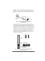
1
BL1000
C-Programmable Controller
User’s Manual
019-0012 · 071031-C
BL1000 User’s Manual
Part Number 019-0012 • Revision C
Last revised on October 31, 2007 • Printed in U.S.A.
Copyright
© 1998–2007 Rabbit Semiconductor, Inc. • All rights reserved.
Rabbit Semiconductor reserves the right to make changes and improvements to its products without providing notice.
Trademarks
®
• Dynamic C is a registered trademark of Z-World, Inc.
™
• PLCBus is a trademark of Z-World, Inc.
Company Address
Rabbit Semiconductor, Inc.
2900 Spafford Street
Davis, California 95616-6809
USA
Telephone:
Facsimile:
Web Site:
E-Mail:
(530) 757-3737
(530) 753-5141
www.rabbit.com
www.rabbit.com/support/
TABLE OF CONTENTS
About This Manual
vii
Overview
1-1
Getting Started
2-1
BL1000 Operation
3-1
System Development
4-1
BL1000 Overview .............................................................................. 1-2
BL1000 Features ................................................................................ 1-3
Software Development and Evaluation Tools .................................... 1-5
Initial BL1000 Setup .......................................................................... 2-2
Parts Required ............................................................................... 2-2
Connecting the BL1000 to a Host PC ................................................ 2-2
Running Dynamic C ........................................................................... 2-5
Test the Communication Line ............................................................ 2-5
Selecting Communications Rate, Port, and Protocol ......................... 2-5
Running a Sample Program ............................................................... 2-6
Operating Modes ...............................................................................
Run Mode ......................................................................................
Changing Baud Rate on the BL1000 ............................................
EPROM ..............................................................................................
Programming EPROMs ................................................................
Choosing EPROMs .......................................................................
Copyrights .....................................................................................
Onboard LED .....................................................................................
3-2
3-3
3-3
3-3
3-3
3-4
3-5
3-5
BL1000 Inputs/Outputs ...................................................................... 4-2
Digital Interfaces ................................................................................ 4-4
PIO Interface ................................................................................. 4-4
Using PIO Ports .......................................................................... 4-6
High-Current/High-Voltage Driver .................................................... 4-8
High-Voltage Driver Software ...................................................... 4-9
Liquid Crystal Display Interface ...................................................... 4-10
LCD Driver Software .................................................................. 4-12
BL1000
Contents s iii
Serial Ports ....................................................................................... 4-13
Asynchronous Serial Ports .......................................................... 4-13
ASCI Status Registers ................................................................. 4-15
ASCI Control Register A .......................................................... 4-17
ASCI Control Register B .......................................................... 4-18
Software Drivers ......................................................................... 4-20
Time/Date Clock .............................................................................. 4-21
Time/Date Functions ................................................................... 4-22
Watchdog Timer ............................................................................... 4-23
Using the Watchdog Timer .......................................................... 4-23
BL1000 Dynamic C Libraries .......................................................... 4-24
Analog Input .................................................................................... 4-25
Analog/Digital Driver ................................................................. 4-25
Signal Conditioning .................................................................... 4-25
Configuration 1 ......................................................................... 4-26
Configuration 2 ......................................................................... 4-26
Configuration 3 ......................................................................... 4-27
Configuration 4 ......................................................................... 4-28
Configuration 5 ......................................................................... 4-29
Configuration 6 ......................................................................... 4-30
Installing Components ................................................................ 4-30
Sources of Error .......................................................................... 4-31
References
5-1
Appendix A: Troubleshooting
A-1
Appendix B: Specifications
B-1
Out of the Box .................................................................................... A-2
Dynamic C Will Not Start .................................................................. A-2
Dynamic C Loses Serial Link ............................................................ A-3
BL1000 Resets Repeatedly ................................................................ A-3
Interrupts Off for Long Periods ......................................................... A-3
Input/Output Problems ....................................................................... A-3
Power-Supply Problems ..................................................................... A-4
Blownout 5841 Driver Chip ..............................................................A-4
Common Programming Errors ........................................................... A-4
Hardware Dimensions ........................................................................ B-2
Jumper and Header Specifications ..................................................... B-4
Wago Connectors .......................................................................... B-6
iv s Contents
BL1000
Appendix C: Memory, I/O Map, and Interrupt Vectors
C-1
Appendix D: EEPROM
D-1
Appendix E: Sample Analog Applications
E-1
Appendix F: Opto 22 Support
F-1
Appendix G: Power Management
G-1
Appendix H: Standalone Programs
H-1
BL1000 Memory ............................................................................... C-2
Physical Memory .......................................................................... C-2
Memory Management ................................................................... C-2
How Dynamic C Uses the MMU .................................................. C-4
Control over Memory Mapping .................................................... C-6
Extended Memory Code ............................................................... C-6
Extended Memory Data ................................................................ C-7
Execution Timing .......................................................................... C-7
Memory-Access Timing ................................................................ C-8
Memory Map ..................................................................................... C-9
Initialized Memory Locations ..................................................... C-13
Interrupt Vectors .............................................................................. C-13
Nonmaskable Interrupts ................................................................... C-14
Power-Fail Interrupts .................................................................. C-14
Jump Vectors .................................................................................... C-15
Interrupt Priorities ............................................................................ C-16
EEPROM Parameters ........................................................................D-2
Library Routines ................................................................................D-3
Semiconductor Temperature Sensor .................................................. E-2
Thermocouple .................................................................................... E-3
420 mA Loop ................................................................................... E-4
Power Consumption ...........................................................................G-2
Intermittent Operation ........................................................................G-3
Option 1: Burn an EPROM ................................................................H-2
Option 2: Use Battery-Backed Static RAM .......................................H-3
Reliability ...........................................................................................H-3
Program Life .................................................................................H-3
Speed .............................................................................................H-4
Data Space ....................................................................................H-4
Cost ...............................................................................................H-4
Ease ...............................................................................................H-4
Remote Downloading ........................................................................H-4
BL1000
Contents s v
Appendix I: Battery
I-1
Storage Conditions and Shelf Life ...................................................... I-2
Replacing the Lithium Battery ............................................................ I-2
Battery Cautions ................................................................................. I-3
Index
Schematic
vi s Contents
BL1000
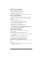
ABOUT THIS MANUAL
This manual provides instructions for installing, testing, configuring, and
interconnecting the Z-World BL1000 controller. Instructions are also
provided for using Dynamic C® functions.
Assumptions
Assumptions are made regarding the user's knowledge and experience in
the following areas:
Ability to design and engineer the target system that a BL1000 will
control.
Understanding of the basics of operating a software program and
editing files under Windows on a PC.
Knowledge of the basics of C programming.
$
For a full treatment of C, refer to the following texts:
The C Programming Language by Kernighan and
Ritchie (published by Prentice-Hall).
and/or
C: A Reference Manual by Harbison and Steel
(published by Prentice-Hall).
Knowledge of basic Z80 assembly language and architecture.
$
For documentation from Zilog, refer to any of the
following texts:
Z180 MPU User's Manual
Z180 Serial Communication Controllers
Z80 Microprocessor Family User's Manual
BL1000
About This Manual s vii
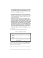
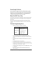
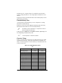
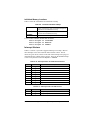
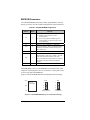
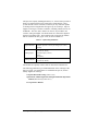
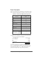
Terms and Abbreviations
Table 1 lists and defines terms and abbreviations that may be used in this
manual.
Table 1. Terms and Abbreviations
Term / Abbreviation
Description
PIO
Programmable Input / Output Integrated Circuit
RAM
Random Access Memory
RTC
Real-Time Clock
SIB
Serial Interface Board
SRAM
Static Random Access Memory
NMI
Nonmaskable Interrupt
Conventions
Table 2 lists and defines typographical conventions that may be used in
this manual.
Table 2. Term and Abbreviation Conventions
Example
Description
While
Courier font (bold) indicates a program, a fragment of a
program, or a Dynamic C keyword or phrase.
// IN-01…
Program comments are written in Courier font, plain face.
Italics
Indicates that something should be typed instead of the
italicized words (e.g., in place of filename, type a file’s
name).
Edit
Sans serif font (bold) signifies a menu or menu selection.
...
An ellipsis indicates that (1) irrelevant program text is
omitted for brevity or that (2) preceding program text may
be repeated indefinitely.
[ ]
Brackets in a C function’s definition or program segment
indicate that the enclosed directive is optional.
byte
To emphasize that certain functions must operate on 8-bit bytes, the term
byte is used as a type specifier. Byte is actually a type character, not a
standard C keyword. Parameters defined by byte are not standard C
characters since they are 8-bit bytes. This function does not work in an
application unless first declared with typedef or #define.
viii s About This Manual
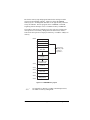
BL1000
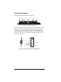
J1
Pin Number 1
A black square indicates
pin 1 of all headers and jumpers.
Pin 1
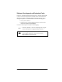
Icons
Table 3 displays and defines icons that may be used in this manual.
Table 3. Icons
Icon
Meaning
$
Refer to or see
(
Please contact
Caution
!
Note
High Voltage
(
BL1000
7,3
Tip
)'
Factory Default
For ordering information, call a Z-World
Sales Representative at (530) 757-3737.
About This Manual s ix
x s About This Manual
BL1000
OVERVIEW
Chapter 1 provides an overview and a brief description of the BL1000
features.
BL1000
Overview s 1-1
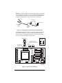
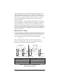
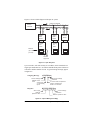
BL1000 Overview
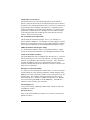
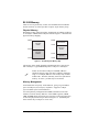
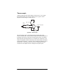
The BL1000 controller is a compact miniature controller that is capable of
handling small control jobs at low cost.
Figure 1-1 illustrates the BL1000 board layout.
LCD Interface
J2
PIO Header
Reset
Button
H6
H5
J3
J9
U1
U2
PIO
Z180
C18
J09
Jack
U14
RS-485 Rx
J16
J11 J12 J13
U12
U4
J15
U10
SRAM
JW2
JW3
U11
J17
C19
U15
L1
C20
D03
U16
JW4
Op-Amps
PAL
U13
ADC
PAL
J10
RS-232
J8
U7
J14
R.T. Clock
U8
EPROM U9 Watchdog
U6
RS-485 Tx
PAL
U5
J7
JW1
U03
EEPROM
XTAL
J19
5841 H.V.
J5
J6
LED
J4
J1
U17
D3
J18
RP4
RP3
RP6
RP5
Figure 1-1. BL1000 Board Layout
1-2 s Overview
BL1000
BL1000 Features
•
Z180 microprocessor running at 9.216 MHz with a partial wait state.
•
Power failure detection and warning. A nonmaskable interrupt takes
place when the supply voltage reaches a certain level. The program has
a few milliseconds to shut down gracefully.
•
Watchdog timer. The watchdog, if enabled, automatically resets the
board if it is not regularly “hit” by the program. This feature helps the
BL1000 to recover from software or hardware failures.
•
Up to 256 kbytes of EPROM. The board accepts either 28-pin or
32-pin chips.
•
Up to 512 kbytes of battery-backed static RAM. Either 28-pin or
32-pin chips may be used. The lithium backup battery mounted on the
board will last up to 10 years with the board installed in normal use.
•
512 bytes of EEPROM. The EEPROM memory can be protected against
erasure by a jumper. This memory may be used to hold the baud rate
and other semipermanent calibration or setup constants.
•
Battery-backed time and date clock based on the Epson 72421 chip.
The clock runs up to 10 years on the lithium battery.
•
Two serial ports based on the built-in ports of the Z180. Both RS-485
(differential) and RS-232 interfaces are available. Either channel can
run with RS-485 drivers. Only Channel 0 can use RS-232 drivers.
•
16-bit parallel port based on the Zilog PIO. This can be directly
interfaced to many devices. The port lines can be programmed as event
lines that cause an interrupt when toggled. Each line has a 10 kΩ pullup resistor.
•
4-bit high-voltage/high-current port based on the Sprague 5841 type
driver. This family of drivers is capable of up to 0.75 A per channel,
with proper heat sinking, at up to 48 V. The drivers are protected
against inductive kickback with integral diodes. They are suitable for
driving solenoids.
•
Liquid crystal display (LCD) interface. LCDs (such as Seiko part
number M1632) can be directly plugged into the 14-pin connector.
Many compatible displays are available in various formats, such as
2 lines by 16 characters, and 4 lines by 40 characters. Graphic displays
are also available.
BL1000
Overview 1-3
Four-channel analog/digital converter with configurable input amplifiers. Input signals can be differentially amplified relative to an offset
for greater measurement precision. The BL1000 interfaces to most
sensors such as strain gauges, thermocouples, semiconductor temperature sensors, thermistors, and 420 mA loops.
A high-efficiency switching regulator, contained completely on the
board, reduces waste heat and accepts a wide range of input voltages.
The switching regulator can also be powered on and off under software
control, allowing intermittent operation (to conserve power) or automatic power-off after a delay.
An optional linear regulator, available on various BL1000 models,
provides up to 0.5 A of +5 V from a DC input of approximately 9 V to
16 V that may be obtained from a wall transformer or by other means.
Field wiring terminations. Most signals that go off the board, including
both analog and digital inputs, high-current outputs and one RS-485
serial communications interface, can be accessed with Wago connectors
that accept up to approximately #18 copper wire. The Wago connectors have spring-loaded clamps that make it easy to install and remove
wires without special tools. The spring action ensures a reliable
connection that will not loosen over time. Standard 0.025 square
computer headers (Berg) can also be used to bring these same signals
off the board.
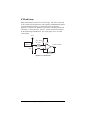
Table 1-1 lists the versions of the BL1000 that are available.
Table 1-1. BL1000 Series Features
Model
Features
BL1000
Standard full-featured model
BL1010
BLl000 with linear regulator instead of switching
regulator
BL1020
BL1000 without analog inputs or Wago connectors,
has linear regulator
BL1030
BL1000 without analog inputs, RS-485, Wago
connectors, time/date clock, or high-current outputs,
has linear regulator
The BL1000 Series is also available with 128K or 512K SRAM factory
installed. A Dynamic C Interface Board frees one RS-232 port during
programming and speeds programming.
$ Appendix B provides detailed specifications for the BL1000.
1-4 s Overview
BL1000
Software Development and Evaluation Tools
Dynamic C, Z-Worlds Windows-based real-time C language development
system, is used to develop software for the BL1000. The host PC downloads the executable code through the BL1000s RS-232 serial port or
through the Dynamic C Interface Board to one of the following places:
battery-backed RAM, or
ROM written on a separate ROM programmer and then substituted for the standard Z-World ROM.
This allows fast in-target development and debugging.
$
Z-Worlds Dynamic C reference manuals provide complete
software descriptions and programming instructions.
(
For ordering information, or for more details about the
various options and prices, call your Z-World Sales
Representative at (530) 757-3737.
BL1000
Overview s 1-5
1-6 s Overview
BL1000
GETTING STARTED
Chapter 2 provides instructions for connecting the BL1000 to a host PC
and running a sample program.
BL1000
Getting Started s 2-1
Initial BL1000 Setup
Parts Required
24 V unregulated DC power supply
Programming cable
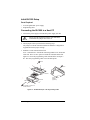
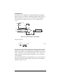
Connecting the BL1000 to a Host PC
1. Connect the power supply to the BL1000 power supply jack J09.
Do not plug the transformer into the wall until all the
connections and jumpers have been set.
2. Check jumpers where specified in the following steps.
The jumpers on the BL1000 board define the hardware configuration.
Appendix B lists the jumper settings.
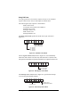
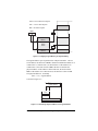
3. Establish a serial communications link.
A PC communicates with the BL1000 using an RS-232 or an RS-485
serial link. There are two options to install the communications link.
Figure 2-1 shows the programming cable included in the developers
kit. The same programming cable is used in both options.
To PC
6
9
1
To PC
5
3M 3631
3M 3473
9
9-pin to 25-pin
adapter
(optional)
2
3
1
To BL1000 or Dynamic C
Interface Board
Figure 2-1. BL1000 Developers Kit Programming Cable
2-2 s Getting Started
BL1000
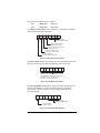
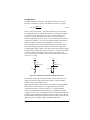
Option 1Use the 10-pin header, J8, an RS-232 serial port on the
BL1000 to connect directly to the PC serial port using the cable shown
in Figure 2-1. Figure 2-2 shows a BL1000 connected directly to the
PC.
To PC
BL1000
Programming
Cable
J8
Transformer
J09
Figure 2-2. Connecting Programming Cable Directly
to BL1000 Header J8
Place a jumper to connect the pins of programming jumper block J4
(near the reset button) on the BL1000. The BL1000 will then read its
setup state from the jumpers on PIO header J9, as shown in Figure 2-3.
The BL1000 uses this setup state after a reset, and also stores the setup
in EEPROM so that the programming jumper J4 and the jumpers on the
PIO header can be removed. The setup state also specifies whether to
run Dynamic C or a program stored in RAM. Change the jumper
settings to connect pins 2-3 on jumper block J16 to remove the write
protection when initializing a new EEPROM, and connect pins 1-2 on
J15 for RS-232 communication.
J15
J9
1
J16
2
Not Used
for Setup
Reserved
Connect to initialize
new EEPROM
9600 19,200 28,800 57,600
Baud Rate
Connect for RS-232 programming via J8
33
Not connected enables LED
34 Connected during programming
= run user program in RAM on reset
Figure 2-3. Jumper Connections for BL1000 PIO Header J9
and Jumper Block J15
BL1000
Getting Started s 2-3
Option 2Connect a Dynamic C Interface Board to the 40-pin header,
J7, on the BL1000. The 40-wire cable is included with the Dynamic C
Interface Board. The Dynamic C Interface Board can handle RS-232
or RS-485 communication. Figure 2-4 shows the connections.
To PC
BL1000
J7
Transformer
J06
J01/J02
Programming
Cable
Dynamic C
Interface
Board
J09
Figure 2-4. Using Dynamic C Interface Board to Program BL1000
Although the Interface Board has its own power supply connections at
J03, as shown in Figure 2-5, do not connect the transformer to the
Interface Board. The Interface Board will receive its power through
the 40-wire cable connecting it to the BL1000.
Baud Rate
BL1000
J15
57,500
28,800
Connect pins 7-8 to
disable Interface Board
(behave as if not connected)
19,200
9600
Connect pins 1-2
to run program
in RAM
RS-485
RS-232
RS-485 RS-232
2 4 6 8 10 12 14 16
J01
15
1
J06
J04
RS-485 RS-232
J07
U03
U01
KIO
U04
U02
J02
U05
Reset
Button
U06
R1
40-pin connection to BL1000
J05
J08
Leave disconnected
Jack
J03
DC Power
Connector
Figure 2-5. Dynamic C Interface Board
2-4 s Getting Started
BL1000
The reset button on the Interface Board is connected in parallel with
the reset button on the BL1000. There are two 10-pin serial headers on
the Dynamic C Interface Board, one for RS-232 communication (J01)
and one for RS-485 communication (J02). Set the jumpers on jumper
block J04 according to whether RS-232 or RS-485 communication will
be used. Pins 3-4 and 5-6 on header J07 are used to set the baud rate.
Connect pins 1-2 on J07 to run the program in the battery-backed RAM
on reset, instead of Dynamic C.
The main advantage of using the Dynamic C Interface Board is that the
RS-232 serial port (J8) is not used up for development purposes.
Another advantage of the Interface Board is that serial communication
uses a nonmaskable interrupt that cannot be disabled by the program.
This form of communication is more robust than a regular serial port.
4. The BL1000 is now ready for programming. The power supply transformer may be plugged in and turned on.
Running Dynamic C
Test the Communication Line
Double-click the Dynamic C icon to start the software. Note that the PC
attempts to communicate with the BL1000 each time Dynamic C is started.
No error messages are displayed once communication is established.
$
See Appendix A, Troubleshooting, if an error message such as
Target Not Responding or Communication Error appears.
!
Once the necessary changes have been made to establish
communication between the host PC and the BL1000, use the
Dynamic C shortcut Ctrl Y to reset the controller and initiate
communication.
Selecting Communications Rate, Port, and Protocol
The communication rate, port, and protocol are all selected by choosing
Serial Options from Dynamic Cs OPTIONS menu.
The BL1000s default communication rate is 19,200 baud. However, the
Dynamic C software shipped by Z-World may be initialized for a different
rate. To begin, adjust the communications rate to 19,200 baud.
Make sure that the PC serial port used to connect the serial cable (COM1
or COM2) is the one selected in the Dynamic C OPTIONS menu. Select
the 1-stop-bit protocol.
BL1000
Getting Started s 2-5
Running a Sample Program
A sample program, TGFLASH.C, is supplied in the Dynamic C SAMPLES
subdirectory. This program flashes the LED on the board.
Prior to running this test, be sure to set the communications parameters in
Dynamic C so that the PC and the BL1000 are handshaking properly.
1. Compile the program by pressing F3 or by choosing Compile from the
COMPILE menu. Dynamic C compiles and downloads the program.
2. Run the program by pressing F9 or by choosing Run from the RUN
menu. The LED on the BL1000 will begin flashing continuously.
4. Press Ctrl Z to stop execution of the program.
5. If needed, press F9 to restart execution of the program.
2-6 s Getting Started
BL1000
BL1000 OPERATION
Chapter 3 describes how to use the BL1000, with a focus on
how to set the run and programming modes, and
how to burn a custom program on EPROM.
BL1000
Operation s 3-1
Operating Modes
A hardware reset takes place when the BL1000 is powered up, when the
reset button is pressed, or when the watchdog timer times out.
If a valid program (created with Dynamic C) has been installed in
EPROM, the program starts running. A valid program is recognized by a
code that Dynamic C places in the file used to burn the EPROM.
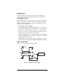
The flowchart in Figure 3-1 shows the startup sequence of the BL1000
after a hardware reset.
Begin from
hardware reset
Valid
program in
EPROM?
Dynamic C
Interface Board
connected?
YES
YES
Run program.
Pins 1-2 on
J07 connected on
Interface
Board?
YES
Run Dynamic C using
baud rate specified by
J07 on Interface Board.
NO
Program
jumper
installed on
J4?
EEPROM
NO
installed?
NO
YES
Read PIO J9 jumpers for
mode and baud rate
EEPROM
installed?
YES
Run application in RAM or
enter error stop mode
Run application in RAM or
enter error stop mode.
Enter mode specified by
contents of EEPROM: run
Dynamic C or application
in RAM.
Make EEPROM agree with
PIO J9 jumpers, flash LED
Enter mode specified by PIO J9 jumpers
Figure 3-1. BL1000 Activity at Startup
3-2 s Operation
BL1000
Run Mode
Before running a program from battery-backed RAM or from an EPROM,
first switch the BL1000 from programming mode to run mode by removing
the jumper connecting the pins on jumper block J4 or by removing the
Dynamic C Interface Board.
The BL1000 will now run the program from RAM if pins 33 and 34 on J9
(or pins 1 and 2 on the Interface Boards J07) were connected during
programming. A program may also run from EPROM.
!
If the Dynamic C EPROM is present on the board, the
BL1000 executes the program stored in battery-backed
RAMthat is, the program last run under Dynamic C. If
the Dynamic C EPROM has been replaced with a custom
EPROM, then the BL1000 executes that program.
Changing Baud Rate on the BL1000
The baud rate may be changed by connecting the appropriate pins on
header J9 as shown in Figure 2-3, with the pins on J4 connected, then
pushing the reset button and disconnecting the pins on J4. Alternatively,
the Dynamic C Interface Board may be connected with the appropriate
pins on its header J07 connected as shown in Figure 2-5, then pressing the
reset button.
Be sure the power to the BL1000 is disconnected before
changing any jumper connections.
EPROM
Programming EPROMs
Dynamic C can be used to create a file for programming an EPROM by
selecting the Compile to File option in the COMPILE menu. The BL1000
must be connected to the PC running Dynamic C during this step because
essential library routines must be uploaded from the Dynamic C EPROM
and linked to the resulting file. The output is a binary file (optionally an
Intel hex format file) that can be used to build an application EPROM.
The application EPROM is then programmed with an EPROM programmer that reads either a binary image or the Intel hex format file. The
resulting application EPROM can then replace the EPROM that came with
the BL1000.
Whenever the Dynamic C EPROM is replaced by a custom EPROM, the
BL1000 ignores the program in battery-backed RAM in favor of the
program stored in EPROM.
BL1000
Operation s 3-3
When doing program development with Dynamic C, it is best to use a
128 kbyte SRAM or larger. Dynamic C will work with a 32 kbyte SRAM,
but the total program space will be limited to 16 kbytes of root and
16 kbytes of extended memory. This is enough for many programs, but it
is inconvenient to run out of memory during development. Once a
program is burned into EPROM, there is no reason to use SRAM larger
than 32 kbytes unless the data space is larger than 32 kbytes.
Choosing EPROMs
Socket U8 can accommodate several different types of EPROMs, including the following.
27C256
27C512
27C010
27C020
32 kbytes
64 kbytes
128 kbytes
256 kbytes
28 pins
28 pins
32 pins
32 pins
When using a 28-pin EPROM, four pin positions at one end of the socket
are left empty, as shown In Figure 3-2.
U7
U1
U8
PAL
PAL
U6
28-pin
EPROM
PAL
PAL
U8
U6
U7
U13
32-pin
EPROM
U13
SRAM
J10
SRAM
J10
J11 J12 J13
J11 J12 J13
Figure 3-2. 28- and 32-pin EPROM Replacement
The corresponding jumper settings for jumper blocks J11, J12, and J13 are
shown in Figure 3-3.
J11
32 kbyte
EPROM
J12
larger
EPROM
28-pin or
128 kbyte
32-pin
EPROM
256 kbyte
EPROM
J13
smaller
SRAM
512 kbyte
SRAM
Figure 3-3. BL1000 Jumper Settings for Different Size SRAM and EPROM
Either 28- or 32-pin SRAM chips may be used.
3-4 s Operation
BL1000
Copyrights
The Dynamic C library is copyrighted. Place a label containing the
following copyright notice on the EPROM whenever an EPROM that
contains portions of the Dynamic C library is created.
©19911993 Z-World, Inc.
Your own copyright notice may also be included on the label to protect
your portion of the code.
Z-World grants purchasers of the Dynamic C software and the copyrighted
BL1000 EPROM permission to copy portions of the EPROM library as
described above, provided that:
1. The resulting EPROMs are used only with the BL1000 controllers manufactured by Z-World, Inc., and
2. Z-Worlds copyright notice is placed on all copies of the EPROM.
Onboard LED
A single LED sits adjacent to jumper block J19 on the BL1000 board.
The LED is only accessed when the programming jumper is installed on
jumper block J4, so it will not interfere with any connections to PIO Port
A, bit 1, which is used to flash the LED. The LED flashes a code to
identify what is happening during programming. An error code consists of
a combination of dots or dashes. A dot turns the LED on for about 0.3 s.
A dash turns the LED on for about 1 s. The codes are listed in Table 3-1.
Table 3-1. LED Message Codes
Pattern
—···
·· —·
····
BL1000
Meaning
The board has been set to run a program in RAM, but
there is no valid user program in EPROM or in batterybacked RAM.
J9 is jumpered to initialize a new EEPROM, but the
EEPROM is write-protected by pins 1-2 on J16 being
connected.
The EEPROM has been rewritten in response to a
jumper change. The code flashes twice.
Operation s 3-5
3-6 s Operation
BL1000
SYSTEM DEVELOPMENT
Chapter 4 provides the following information to develop the BL1000 for
specific uses.
BL1000 inputs/outputs
Digital interfaces
Serial ports
Time/date clock
Watchdog timer
Analog input
BL1000
System Development s 4-1
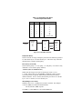
BL1000 Inputs/Outputs
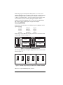
Figure 4-1 illustrates the BL1000 pin assignments.
JW4
JW3
8
1
8
JW2
1
8
JW1
1
8
1
Figure 4-1. BL1000 Pin Locations
Figure 4-2 illustrates the liquid crystal display interface at header J1. Note
that the pins on this header are numbered in a mirror image to the usual
numbering scheme. This numbering scheme matches that of Seiko LCD
units; other manufacturers pin numbers may vary. LCD units that require
a negative voltage can be connected to the -10 V supply from the RS-232
driver at jumper block J3.
J1
-10 V
1
2
3
J3
D6
D4
D2
D0
/Wr
contrast - VSS
+5 V - VDD
2
1
14
13
D7
D5
D3
D1
LCD - select
A0
GND
Figure 4-2. Header J1 LCD Interface Pin Assignments
4-2 s System Development
BL1000
Table 4-1 lists the signals on each pin.
Table 4-1. BL1000 I/O Connector Pins
Connector
Pin
Signal
1
2
3
4
5
6
7
8
Bit 7 and bit 3, high-current/high-voltage driver
Bit 6 and bit 2, high-current/high-voltage driver
Bit 5 and bit 1, high-current/high-voltage driver
Bit 4 and bit 0, high-current/high-voltage driver
K (clamp diodes)
SUB (substrate, most negative)
Ground, high-current/high-voltage driver
VCC (+5 V)
1
2
3
4
5
6
7
8
Analog REF (+2.5 V), output impedance about 300 Ω
Digital ground
RXA1 receive, RS-485 Channel 1
–RXA1 receive, RS-485 Channel 1
TXA1 transmit, RS-485 Channel 1
–TXA1 transmit, RS-485 Channel 1
Digital ground
+9 V in, unregulated input for onboard supplies (used
as alternate to plug J09, more than 9 V is acceptable)
RXA0 receive, RS-485 Channel 0
JW3
1
2
3
4
5
6
7
8
CH0L analog input Channel 0, low
JW4
1
2
3
4
5
6
7
8
JW1
JW2
BL1000
–RXA0 receive, RS-485 Channel 0
TXA0 transmit, RS-485 Channel 0
–TXA0 transmit, RS-485 Channel 0
Digital ground
CH3L analog input Channel 3, low
CH3H analog input Channel 3, high
+5 V analog (filtered VCC)
CH0H analog input Channel 0, high
Analog ground
CH1L analog input Channel 1, low
CH1H analog input Channel 1, high
Analog ground
CH2L analog input Channel 2, low
CH2H analog input Channel 2, high
System Development s 4-3
Digital Interfaces
PIO Interface
The Zilog Z80 PIO interface chip at U2 is a 44-pin LSI chip that provides
16-bit parallel I/O lines, each of which may be individually set up as an
input or an output. The lines may also be used to detect transitions and
cause an interrupt in the microprocessor in various ways. Figure 4-3
illustrates the interface.
+5 V
J9
10 kΩ
PB7
10 kΩ
+5 V
1
3
PB6
5
PB5
7
PB4
9
PB3
11
PB2
13
PB1
PB0
15
17
PA7
19
PA6
21
PA5
23
PA4
25
PA3
27
PA2
29
PA1
31
PA0
33
/BSTB1
/ASTB1
H6
H5
BRDY1
ARDY1
+5 V
Figure 4-3. Zilog Z80 PIO Interface Chip
Lines PA0PA7 are considered Port A and lines PB0PB7 are considered Port B. Each line can serve as an input or output in different
modes. The four lines on H5 and H6 are handshaking lines, and consist of
a ready line and a strobe line for each port.
The PIO can read a cross-wire keypad by setting each row to zero volts
and monitoring each column; the columns are held up by pull-up resistors.
The microprocessor uses the PIO chip to detect closures of any of the keys
in the keypad. Debouncing must be done by software.
The impedance of the PIO chip is approximately 80 Ω for sinking current
and 160 Ω for sourcing current. Voltages below ground or above VCC
should not be applied to the PIO.
4-4 s System Development
BL1000
The PIO is flexible and has a number of modes of operation. The two
ports are controlled by the following four registers.
0B000H
(PIODA) PIO Port A, data
0B001H
(PIODB) PIO Port B, data
0B002H
(PIOCA) PIO Port A, command
0B003H
(PIOCB) PIO Port B, command
Each register pair controls one of the 8-bit ports and the two handshaking
lines associated with each port. The four modes of operation of the ports
are as follows.
Mode 0strobed byte output.
Mode 1strobed byte input.
Mode 2bidirectional data transfer (Port A only).
Mode 3bitwise I/O, input/output selectable per bit.
Mode 0 (Strobed Byte Output)
When the microprocessor stores a byte in a ports data register, the eight
associated output lines change their level according to how each bit is set,
to high for a 1 and low for a 0. The ready handshake line goes high.
When an external device pulses the strobe line (low), the ready line is
reset. If interrupts are enabled for the port, a PIO interrupt is requested.
This allows for interrupt-driven parallel output.
Mode 1 (Strobed Byte Input)
The PIO latches eight bits into a register upon the strobe signal from an
external device. The strobe signal also causes the ready line to go low. An
interrupt is then requested. After the microprocessor reads the register, the
ready line is raised to indicate that the port is ready for another byte.
Mode 2 (Bidirectional Data Transfer)
This mode uses Port A and all four handshake lines. It allows data to be
transferred in both directions under control of the four handshake lines.
Mode 3 (Bitwise I/O)
This is a general-purpose input-output mode. Each bit can be individually
specified as input or output. In this mode, the input lines can also serve as
interrupt request lines. Either transition to high or transition to low can be
specified for the interrupt request. Interrupts for specific input lines are
controlled with a mask and by specifying an AND or an OR function for
the masked lines. Interrupts on PIO ports are edge triggered.
BL1000
System Development s 4-5
Using PIO Ports
To set up a port for I/O, first write a sequence of bytes to its command
register. Then read, or write, its data register to transfer data.
The control register byte sequence is shown below.
Mode control word
I/O register control word (only if Mode 3)
Interrupt vector word
Interrupt control word
Mask control word
Interrupt disable word
The mode control word specifies the mode for the port as shown in
Figure 4-4.
D7
D6
X
X
1
1
1
1
Identifies this as the
mode control word
0 0 = Mode 0
0 1 = Mode 1
1 0 = Mode 2
1 1 = Mode 3
Figure 4-4. PIO Mode Control Word
The I/O register control word, shown in Figure 4-5, must immediately
follow the mode control word, but only when the mode is 3 (bitwise I/O).
This specifies which bits are inputs and which bits are outputs for bitwise I/O.
D7
D6
D5
D4
D3
D2
D1
D0
0 bit is output
1 bit is input
Figure 4-5. PIO Register Control Word
The interrupt vector word, shown in Figure 4-6, specifies the interrupt
vector for the particular PIO channel.
D7
D6
D5
D4
D3
interrupt vector
D2
D1
0
Identifies this as
interrupt vector word
Figure 4-6. PIO Interrupt Vector Word
4-6 s System Development
BL1000
The vectors for the PIO ports are as follows.
0x12
(PIOA_VEC)
PIO Port A
0x14
(PIOB_VEC)
PIO Port B
The interrupt control word, shown in Figure 4-7, specifies the conditions
under which an interrupt is generated.
D7
D6
D5
D4
0
1
1
1
Identifies this as
interrupt vector word
0 No mask word follows
1 Mask word follows
0 Active level for interrupt is low
1 Active level is high
0 Interrupt on OR function
1 Interrupt on AND function
0 Interrupt disabled
1 Interrupt enabled (after M1)
Figure 4-7. PIO Interrupt Control Word
The mask control word, shown in Figure 4-8, must immediately follow the
interrupt control word if bit D4 of the interrupt control word is set.
D7
D6
D5
D4
D3
D2
D1
D0
Mask bits: A bit is monitored and an interrupt
is generated if the bit is set as input and the
mask bit is set to 0. Do not set a bit
specified as output as a mask bit.
Figure 4-8. PIO Mask Control Word
The interrupt disable word, shown in Figure 4-9, allows an interrupt to be
enabled or disabled for a port that is already defined by an interrupt
control word. This byte can also be used to disable interrupts on an
unconfigured port.
D7
X
X
X
0
1
1
1
Identifies this as
interrupt disable word
0 Interrupt disable
1 Interrupt enable
Figure 4-9. PIO Interrupt Disable Word
BL1000
System Development s 4-7
High-Current/High-Voltage Driver
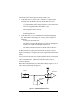
Figure 4-10 shows a diagram of the high-current/high-voltage driver.
The BL1000, BL1010, and BL1020 use the Allegro (Sprague) 5841 chip.
!
The BL1000 is only rated to 48 V dc, even though some of
its chips have higher voltage ratings.
Inductive Load
Voltage In
Max 35 V 5841A
50 V 5842A
50 V 5843A
Solenoid
JW1
Bit 7
Bit 6
Serial
Interface
Bit 5
from
Sample
Circuit
Bit 4
Z180
K
SUB
5841
+24 V
+
GND
Power
Supply
GND
VCC
Optional
Cap
Figure 4-10. BL1000 High-Current/High-Voltage Driver
The following ICs may also be used for the high-current driver.
Driver
UCN-5841A
UCN-5842A
UCN-5843A
Breakdown Sustained
50 V
80 V
100 V
35 V
48 V
48 V
Each channel is capable of sinking up to 0.5 A. Since two channels are
paralleled for each output from the board, up to 1.0 A can be driven by
each output, although a more conservative rating would be 0.80 A to allow
for mismatches between the channels. The maximum power dissipation
allowed is 2.2 W at 25°C. Derate this above 25°C. The allowed power
dissipation at 70°C would be 1.1 W. The collector to emitter voltage is
rated at a maximum of 1.6 V at 350 mA, and 1.1 V at 100 mA. To
compute the power dissipation, multiply the current by the collector to
emitter voltage. If 200 mA flows, then each driver on the chip will see
4-8 s System Development
BL1000
100 mA, and the power dissipation will be 1.1 V × 0.2 A = 0.22 W.
Driving four loads at the same time, it is reasonable for each load to sink
200 mA since the total power dissipation would be 0.88 W, below the
1.1 W rating at 70°C.
The SUB pin can be up to 20 V negative with respect to ground, such as
when using split power supplies, but it is important that the ground be
located between the plus and minus power supply voltage (no floating
supply). A jumper (J19) is provided to ground SUB when no other input is
connected. If nothing else is connected to SUB, then this jumper should be
in place to prevent possible chip overheating from a floating SUB line.
When the chip is connected, the SUB terminal should be connected
properly, rather than relying on the board jumper, which may not be able to
handle large currents. This driver can drive inductive loads such as
solenoids or relays. The K terminal carries inductive overshoot back to the
power supply. If the wire carrying the K signal is long, a local filter
capacitor should be installed near the board to absorb the inductive spike
(see the optional capacitor in Figure 4-10).
When driving incandescent lights, beware of the initial inrush current
stressing the driver.
It is not advisable to use the unregulated DC into the board
for power drive if the load will trigger the BL1000s power
failure circuitry. If the unregulated input to the board is
used, be sure to take the current directly from the supply and
not from the board connector. It is easy to blow out the
5841 chip by connecting and removing wires with the power
enabled. If the protective diodes are not connected,
inductive loads will promptly blow out the chip.
High-Voltage Driver Software
The following functions (in DRIVERS.LIB) provide access to the 5841A
high-voltage driver.
int hv_wr( byte value )
Writes the byte value to the driver. The most significant four bits of
the byte affect the driver. The output enable remains the same. All
four bits are strobed to the output register in one clock, so all bits
change simultaneously. A 1 enables the corresponding output (pulls
low). A 0 disables the corresponding output.
BL1000
System Development s 4-9
This function uses the Z180 CSIO serial interface to transmit one
character to the high-voltage driver chip and could conflict with drivers
for the A/D converter if used at a different priority level. The relationship between the bits and the output signals is as follows.
bit 7, 3
bit 6, 2
bit 5, 1
bit 4, 0
output 1
output 2
output 3
output 4
The upper four bits in the byte are replicated in the lower four bits
before being sent to the driver so that, if the driver is a 5841, the
parallel channels work together.
int hv_enb()
int hv_dis()
Enables or disables, respectively, the high-voltage driver chip. The
functions enable or disable all four outputs at the same time, without
changing the values of the bits in the drivers internal register.
A hardware reset occurs when the high-voltage driver output is
disabled.
If the driver chip fails because of stress, it can fail in the ON
state, allowing current to flow. Be sure to consider the
consequences of any such failure and take appropriate
precautions when necessary.
Liquid Crystal Display Interface
Connector J1 serves as an interface to standard liquid crystal displays
(LCDs) that use a 14-pin connector and are compatible with the Hitachi
HD44780 LCD driver chip. Figure 4-11 shows the pin assignments.
The cable connects to the bottom side of LCD modules such as the Seiko
M1632 (16 characters by 2 lines). Therefore, the J1 connector is numbered in a mirror image compared to a standard 14-pin connector. Carefully analyze the connector pin assignments before ordering an LCD unit
since units vary slightly.
The LCD driver has two registers accessed at the following I/O addresses.
LCD
LCD + 1
0A000H
0A001H
control register
data register
Figure 4-12 shows the timing chart for the LCD.
4-10 s System Development
BL1000
Pin 2
Pin 1
LCD
Display
Pin 14
J1
-10 V
D6
D4
D2
D0
/Wr
J3
contrast - VLC
+5 V - Vdd
2
1
14
13
D7
D5
D3
D1
LCD - select
A0
Vss - ground
Figure 4-11. BL1000 J1 LCD Interface Pin Assignments
T0
T1
TW1
TW2
TW3
TW4
T3
A0 RS
/WR
LCD
PWCH = 450 ns
TAS setup time 140 or 60 ns required
Figure 4-12. LCD Timing Chart
Two conditions in this timing chart may be difficult to meet if certain
precautions are not observed.
1. The timings in Figure 4-12 are for the Hitachi 44780 LCD chip. TAS
must be at least 140 ns and PWCH must be 450 ns. However, many
LCDs use the Hitachi 44780A instead of the 44780 controller. With
the 44780A, the setup time TAS is only 60 ns, and the pulse width PWCH
required is only 300 ns.
BL1000
System Development s 4-11
2. The Z180 internal control register bit IOC must be set to 0 for the
timing to be correct for the LCD. This is the software default.
LCD Driver Software
The following library functions in DRIVERS.LIB drive a 2-line by
16-character LCD such as the Seiko M1632.
void lcd_init ( int mode )
Initializes the display. For the M1632, mode is set to 0x18.
int lputc( int ch )
Sends one character to the display. These special characters can be
sent to control the display. These characters all have bit 7 set to 1.
\xF0 clear line 0
\xF1 clear line 1
\xF2 cursor off, stop cursor blink
\xF3 cursor on
\xF4 cursor to blinking mode
\xF5 shift display left
\xF6 shift display right
\x80 codes 80, 81, etc. position cursor at column 0, 1, etc. on line 0
\xC0 codes C0, C1, etc. position cursor at column 0, 1, etc. on line 1
\n position cursor to first column of second line
char *lputs( char *string )
Sends a null-terminated string to the LCD.
int lprintf( char *,... )
The function lprintf is the same as printf with output to the LCD
driver.
4-12 s System Development
BL1000
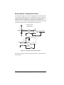
Serial Ports
The BL1000 has two serial ports built into the board. These are a part of
the Z180 processor, as shown in Figure 4-13.
Z180 Processor
Serial
Port 1
RS-485
Serial Driver
Serial
Port 0
RS-485
Serial Driver
Microprocessor
DMA
Counter Timer
DMA
Counter Timer
RS-232
Serial Driver
Figure 4-13. BL1000 Serial Ports
The RS-485 serial ports are brought out to Wago Connectors. The RS-232 serial
port is brought out the 10-pin header J8, where it may be easily converted to an
IBM-style D connector using standard mass termination cables.
$
See Figure 2-1 in Chapter 2, Getting Started, for an illustration of such a cable.
Serial Port 0 must be jumpered at J-15 as either RS-485 or as RS-232. See
Figure 4-14.
J15
J15
RS-232
RS-485
Figure 4-14. Jumper Block J15 Settings for Z180 Serial Port 0
Asynchronous Serial Ports
The Z180 has two independent, full-duplex asynchronous serial channels,
with a separate baud rate generator for each channel. The baud rate is
divided down from the microprocessor clock.
The microprocessor clock frequency should be in the series: 3.072 MHz,
4.675 MHz, 6.144 MHz, 9.216 MHz, and 12.288 MHz, assuming that
standard baud rates must be generated. The crystal will be stamped with
twice this frequency. One of the internal DMA controllers may be used in
conjunction with the internal serial ports.
BL1000
System Development s 4-13
There are two series of baud rates available, one derived by dividing the
microprocessor clock by 1, the other from dividing by 3, both followed by
binary division steps. The baud rates available for a 9.216 MHz clock
appear below.
57,600 28,800 14,400...
19,200 9600 4800...
A built-in function, z180baud, computes the necessary values to store in
the control registers to set up a particular baud rate.
The serial ports have an optional multiprocessor communications feature.
When enabled, an extra bit is included in the transmitted character, where
the parity bit would normally go. Receiving Z180s can be programmed to
ignore all received characters except those with the extra multiprocessing
bit set. This provides a 1-byte attention message that can be used to wake
up a processor without the processor having to monitor all the traffic on a
shared communication link.
The block diagram in Figure 4-15 shows Serial Channel 0. Serial Channel 1 is similar, but modem control lines RTS1 and DCD0 are not
available. Five of the seven registers shown above are directly accessible
as internal I/O registers.
microprocessor internal bus
RXA0
RDR0
TDR0
RSR0
TSR0
Shift Register In
RTS0
CTS0
DCD0
CNTLA0
CNTLB0
Baud Rate
Generator
TXA0
Shift Register Out
CLKA0
STAT0
Figure 4-15. Z180 Serial Channel 0
A separate interrupt vector is used by each of the two channels. The
interrupt vectors are SER0_VEC and SER1_VEC. Channel 0 has the higher
priority.
4-14 s System Development
BL1000
The serial ports can be polled or interrupt-driven. A polling driver tests the
ready flags (TDRE and RDRF) until a ready condition appears (transmitter
data register empty or receiver data register full). If an error condition
occurs on receive, the routine must clear the error flags and take appropriate action, if any. If the CTS line is used for flow control, transmission of
data is automatically stopped when CTS goes high because the TDRE
flag is disabled. This prevents the driver from transmitting more characters because the driver thinks the transmitter is not ready. The transmitter
will still function with CTS high, but care should be exercised since TDRE
is not available to synchronize proper loading of the data register (TDR).
An interrupt-driven port works when the receiver interrupt is enabled as
long as the program wants to receive characters. The transmitter interrupt
is enabled only while characters are waiting in the output buffer. When an
interrupt occurs, the interrupt routine must determine the cause: receiver
data register full, transmitter data register empty, receiver error, or /DCD0
pin high (Channel 0 only). None of these interrupts is edge-triggered and
another interrupt will occur immediately if interrupts are re-enabled
without disabling the condition causing the interrupt. /DCD0 is especially
treacherous because it cannot be disabled while leaving receive interrupts on.
!
Z-World recommends connecting /DCD0 directly to
ground to avoid these problems.
ASCI Status Registers
The Z180 incorporates an asynchronous serial communication interface
(ASCI) that supports two independent full-duplex channels. Appendix C
summarizes the addresses of these registers. A status register for each
channel provides information about the state of each channel and allows
interrupts to be enabled and disabled.
STAT0 (04H)
7
6
5
4
3
2
1
0
RDRF
OVRN
PE
FE
RIE
/DCD0
TDRE
TIE
R
R
R
R
R/W
R
R
R/W
STAT1 (05H)
7
6
5
4
3
2
1
0
RDRF
OVRN
PE
FE
RIE
CTS1E
TDRE
TIE
R
R
R
R
R/W
R/W
R
R/W
BL1000
System Development s 4-15
/DCD0 (Data Carrier Detect)
This bit echoes the state of the /DCD0 input pin for Serial Channel 0.
However, when the input to the pin switches from high to low, the data bit
switches low only after STAT0 has been read. The receiver is held reset as
long as the input pin is held high. This function is not generally useful
because an interrupt is requested as long as /DCD0 is a 1. This forces the
programmer to disable the receiver interrupts to avoid endless interrupts.
A better design would cause an interrupt only when the state of the pin
changes. This pin is tied to ground.
TIE (Transmitter Interrupt Enable)
This bit masks the transmitter interrupt. If set to 1, an interrupt is requested whenever TDRE is 1. The interrupt is not edge triggered. This bit
must be set to 0 when there is a need to stop sending. Otherwise, interrupts
will be requested continuously as soon as the transmitter data register is empty.
TDRE (Transmitter Data Register Empty
A 1 means that the channel is ready to accept another character. A high
level on the /CTS pin forces this bit to 0 even though the transmitter is ready.
CTS1E (CTS Enable, Channel 1)
The signals RXS and CTS1 are multiplexed on the same pin. A 1 stored in
this bit selects the pin to serve the CTS1 function. A 0 selects the RXS
function. (The pin RXS is the CSIO data receive pin.) The CTS line has
no effect when RXS is selected. It is not advisable to use the CTS1
function on the BL1000 because the RXS line is needed to control several
other devices on the board.
RIE (Receiver Interrupt Enable)
A 1 enables receiver interrupts and 0 disables them. A receiver interrupt is
requested under any of the following conditions: /DCD0 (channel 0 only),
RDRF (receiver data register full), OVRN (overrun), PE (parity error), FE
(framing error). The condition causing the interrupt must be removed
before interrupts are re-enabled, or another interrupt will occur. Reading
the receiver data register (RDR) clears the RDRF flag. The EFR bit in
CNTLA is used to clear the other error flags.
FE (Framing Error)
A stop bit was missing, indicating scrambled data. This bit is cleared by
the EFR bit in CNTLA.
PE (Parity Error)
Parity is tested only if MOD1 in CNTLA is set. This bit is cleared by the
EFR bit in CNTLA.
4-16 s System Development
BL1000
OVRN (Overrun Error)
Overrun occurs when bytes arrive faster than they can be read from the
receiver data register. The receiver shift register (RSR) and receiver data
register (RDR) are both full.
RDRF (Receiver Data Register Full)
This bit is set when data are transferred from the receiver shift register to
the receiver data register. It is always set when one of the error flags is set,
in which case defective data are loaded to RDR. The bit is cleared when
the receiver data register is read, when the /DCD0 input pin is high, and by
RESET and IOSTOP.
ASCI Control Register A
Control Register A affects various aspects of the serial channel operation.
CNTLA0 (00H)
7
6
5
4
3
2
1
0
MOD2
MOD1
MOD0
MPE
RE
TE
/RTSO
MPBR/
EFR
R/W
R/W
R/W
R/W
R/W
R/W
R/W
R/W
5
4
3
2
1
0
MOD2
MOD1
MOD0
R/W
R/W
R/W
CNTLA1 (01H)
7
6
MPE
RE
TE
R/W
R/W
R/W
MPBR/
CKA1D
EFR
R/W
R/W
MOD0MOD2 (Data Format Mode Bits)
MOD0 controls stop bits: 0 ⇒ 1 stop bit, 1 ⇒ 2 stop bits. If 2 stop bits
are expected, then 2 stop bits must be supplied.
MOD1 controls parity: 0 ⇒ parity disabled, 1 ⇒ parity enabled. (See
PEO in ASCI Control Register B for even/odd parity control.)
MOD2 controls data bits: 0 ⇒ 7 data bits, 1 ⇒ 8 data bits.
MPBR/EFR (Multiprocessor Bit Receive/Error Flag Reset)
Reads and writes on this bit are unrelated. Storing a byte when this bit is 0
clears all the error flags (OVRN, FE, PE). Reading this bit obtains the
value of the MPB bit for the last read operation when multiprocessor mode
is enabled.
/RTS0 (Request to Send, Channel 0)
Store a 1 in this bit to set the RTS0 line from the Z180 high. This line is
further inverted by the output driver. This bit is essentially a 1-bit output
port without other side effects.
BL1000
System Development s 4-17
CKA1D (CKA1 Disable)
This bit controls the function assigned to the multiplexed pin (CKA1/
TEND0): 1 ⇒ TEND0 (a DMA function) and 0 ⇒ CKA1 (external clock
I/O for Channel 1 serial port).
TE (Transmitter Enable)
This bit controls the transmitter: 1 ⇒ transmitter enabled, 0 ⇒ transmitter
disabled. When this bit is cleared, the processor aborts the operation in
progress, but does not disturb TDR or TDRE.
RE (Receiver Enable)
This bit controls the receiver: 1 ⇒ enabled, 0 ⇒ disabled. When this bit is
cleared, the processor aborts the operation in progress, but does not disturb
RDR, RDRF, or the error flags.
MPE (Multiprocessor Enable)
This bit (1 ⇒ enabled, 0 ⇒ disabled) controls multiprocessor communication mode which uses an extra bit for selective communication when a
number of processors share a common serial bus. This bit has effect only
when MP in Control Register B is set to 1. When this bit is 1, only bytes
with the MP bit on will be detected. Others are ignored. All bytes
received are processed if this bit is 0. Ignored bytes do not affect the error
flags or RDRF.
ASCI Control Register B
Control Register B for each channel configures the multiprocessor mode,
parity, and baud rate selection.
CNTLB0 (02H) and CNTLB1 (03H)
7
6
5
4
3
2
1
0
MPBT
MP
/CTS
PS
PEO
DR
SS2
SS1
SS0
R/W
R/W
R/W
R/W
R/W
R/W
R/W
R/W
SS (Source/Speed Select)
Coupled with the prescaler (PS) and the divide ratio (DR) The SS bits
select the source (internal or external clock) and the baud rate divider, as
shown in Table 4-2.
The prescaler (PS), the divide ratio (DR), and the SS bits form a baud-rate
generator (see Figure 4-16).
4-18 s System Development
BL1000
Table 4-2. Baud Rate Divide Ratios
for Source/Speed Select Bits
Processor
Clock
SS2
SS1
SS0
Divide Ratio
0
0
0
0
1
1
1
1
0
0
1
1
0
0
1
1
0
1
0
1
0
1
0
1
÷1
÷2
÷4
÷8
÷ 16
÷ 32
÷ 64
external clock
Prescaler
(PS)
Divide
Ratio
(DR)
Divider
÷10
or
÷30
1
2
...
64
External
Clock
16
or
64
Figure 4-16. Baud-Rate Generator
DR (Divide Ratio)
This bit controls one stage of frequency division in the baud-rate generator.
If 1 then divide by 64. If 0 then divide by 16. This is the only control bit
that affects the external clock frequency.
PEO (Parity Even/Odd)
This bit affects parity: 0 ⇒ even parity, 1 ⇒ odd parity. It is effective only
if MOD1 is set in CNTLA (parity enabled).
CTS/PS (Clear to Send/Prescaler)
When read, this bit gives the state of external pin /CTS: 0 ⇒ low,
1 ⇒ high. When /CTS pin is high, RDRF is inhibited so that incoming
receive characters are ignored. When written, this bit has an entirely
different function. If a 0 is written, the baud rate prescaler is set to divide
by 10. If a 1 is written, it is set to divide by 30.
MP (Multiprocessor Mode)
When this bit is set to 1, multiprocessor mode is enabled. The multiprocessor bit (MPB) is included in transmitted data.
start bit, data bits, MPB, stop bits
The MPB is 1 when MPBT is 1 and 0 when MPBT is 0.
BL1000
System Development s 4-19
MPBT (Multiprocessor Bit Transmit)
This bit controls the multiprocessor bit (MPB). The MPB is 1 when
MPBT is 1 and 0 when MPBT is 0. When the MPB is 1, transmitted bytes
will get the attention of other units listening only for bytes with MPB set.
Software Drivers
A function to compute the control word for CNTLB0/CNTLB1 is built
into the following function call.
int z180baud( int clock, int baud )
This functions return the byte to be stored in CNTLB0/CNTLB1, considering only the bits needed to set the baud rate. Both the clock and baud rates
are expressed in multiples of 1200. Thus a 9.216 MHz clock is expressed
as 7680 and 19,200 baud is expressed by 16. The return value is 1 if the
baud value cannot be derived from the given clock frequency.
Each port is supported by four routines that control initialization, sending,
receiving, and resetting. These routines are full-duplex, buffer-oriented,
and interrupt-driven. The libraries can be modified since they are in
source code. The libraries are listed below.
int
int
int
int
ser_init_z0( byte mode, byte baud ) // z0
ser_send_z0( char* buf, byte* count )
ser_rec_z0 ( char* buf, byte* count )
ser_kill_z0()
int
int
int
int
ser_init_z1( byte mode, byte baud ) // z1
ser_send_z1( char* buf, byte* count )
ser_rec_z1 ( char* buf, byte* count )
ser_kill_z1()
The functions ser_init_z0 and ser_init_z1 set up the appropriate
serial communications buffer. The mode parameter is a set of flags, as
shown below. The baud parameter is expressed in multiples of 1200 Hz.
bit 0
0
1
1 stop bit
2 stop bits
bit 1
0
1
no parity
parity enabled
bit 2
0
1
7 bit data
8 bit data
bit 4
0
1
even parity
odd parity
For example, the statement below would initialize Port Z0 to communicate
with 8 data bits, no parity, and 1 stop bit at 9600 baud.
ser_init_z0(4,9600/1200);
4-20 s System Development
// Initialize ZIO port 0
BL1000
A data transfer between a buffer and the serial port may begin using send
and receive functions once initialization has been performed. The count
parameter is decremented as characters are transferred. When count
reaches zero, the transfer stops and the serial port is disabled. The calling
program can monitor count to see the progress of the transfer. The kill
function immediately turns off both send and receive.
It is important to remember that send and receive are interrupt-driven.
This means that the transmission will continue in the background while the
program is doing other things. Pointers are passing to a counter and a
buffer. Both the counter and the buffer are changed by the interrupt
routines. Always use static or global variables for the counter and buffer.
A demonstration program, SER_DEMO.C, is provided to demonstrate the
use of the serial driver.
!
The stack and the program will be corrupted if pointers to
function variables stored on the stack are passed to the
interrupt service routine and then that function is exited.
!
Make count a shared variable if the library functions are
modified so that count is larger than a byte.
Time/Date Clock
The battery-backed real-time clock is based on Epsons RTC-72421 clock
chip. The 72421A is accurate to approximately one second per day. The
73421B is accurate to approximately five seconds per day. Time values
are resolved to one second and extend up to 80 years in the future. A
Dynamic C sample program (SETCLOCK.C) is provided to read and write
the clock chip. The lithium battery should keep the clock going for about
10 years unless the board is stored at high temperature for long periods
with the power off.
The clock appears as 16 I/O registers having addresses 0D000H to
0D00FH. The 16 registers use four bits; the upper four bits of the register
are undefined. The 4-bit registers are mostly binary-coded decimal
numbers making up the date and time. The following steps refer to these
registers.
1. Set the 12/24 bit to 1 for 24-hour mode and 0 for 12-hour mode. The
AM/PM bit will be 1 for PM. Mask out this bit in 24-hour mode.
2. The days of the week are represented by 0 for Sunday through
6 for Saturday.
3. Leap year is automatically taken into account.
BL1000
System Development s 4-21
4. Set the year to 90 for 1990, to 91 for 1991, and so on.
5. Constant reading of the clock (say, in a tight loop) will create a loss of
accuracy.
Appendix C shows how the registers are arranged.
Time/Date Functions
Date/time functions can be found in DRIVERS.LIB. The sample program
SETCLOCK.C provides a keyboard interface to display and set the time/
date clock.
The following structure is defined to holds the date and time.
struct
byte
byte
byte
byte
byte
byte
byte
} tm;
{
tm_sec;
tm_min;
tm_hour;
tm_mday;
tm_mon;
tm_year;
tm_wday;
//
//
//
//
//
//
//
seconds 0-59
minutes 0-59
24-hour time 0-23
day of month 1-31
month 1-12
90=1990, 101=2001
0=Sun...6=Sat
Time can also be expressed as seconds since January 1, 1980 (that is,
midnight December 31, 1979). The following functions are provided to
read the time/date clock. Note that it takes about 600 µs to read the clock
chip.
int tm_rd( struct tm *value )
Reads the real-time clock and returns zero if successful, or 1 otherwise. The date/time value is passed back in *value.
ulong clock()
Reads the 72421 timer and returns the time as seconds since January 1,
1980.
int tm_wr( struct tm *value )
Writes the date and time, passed in *value, to the clock and returns 0
if successful and 1 otherwise.
ulong mktime( struct tm *value )
Converts time, passed as *value, into time expressed as seconds since
January 1, 1980. Does not access the timer chip.
int mktm( struct tm *value, long time )
Converts time, expressed as seconds since January 1, 1980, into the
structure *value. Does not access timer chip.
4-22 s System Development
BL1000
Watchdog Timer
The watchdog timer is a reliability feature. If the watchdog timer is
enabled by connecting the pins on jumper block J10, a timer starts running,
and is reset by calling the library function hitwd. If the timer runs for 1.6
s without being reset, the watchdog times out, forcing the BL1000 into a
hardware reset condition for 50 ms, after which the board resumes operation as if the power had just been turned on. It is possible to distinguish
between a power-on reset and a watchdog reset. The watchdog is automatically hit frequently during debugging under Dynamic C. However,
if a program without watchdog hits is started while the pins on J10 are
connected, a reset will take place after 1.6 s and Dynamic C will report a
loss of communication.
void hitwd()
This function hits the watchdog timer. That is, it resets the timers
counter, postponing a hardware reset for another 1.6 s.
int wderror()
This function returns nonzero if the most recent reset was caused by the
watchdog timer. If the reset was caused by a power-on or by the reset
pushbutton, the function returns zero.
Using the Watchdog Timer
The watchdog timers purpose is to cause a recovery from a fault condition, such an endless loop or an invalid microprocessor state. Such a fault
can be caused by an electrical transient or by a software bug. An electrical
transient can generate a microprocessor state that would be impossible
during normal operation. A transient effect strong enough to upset the state
of the microprocessor or erase part of the memory can be much weaker
than that needed to cause permanent damage. The ability to recover from
such faults improves system reliability under stressful environmental
conditions.
Software bugs that only occur once a week or once a year and cause the
program to enter an endless loop are not unusual, and are difficult to
correct. The following scenarios could result.
1. The stack overflows only when a rare sequence of events takes place
(such as an interrupt when a seldom-executed, deeply nested piece of
code is executing). If that code is executed for only 10 µs every 5 min,
and the interrupts take place on average only once every hour, then the
program will probably crash about once a year.
BL1000
System Development s 4-23
2. A multibyte variable is shared between a high-level function and an
interrupt service routine, and proper precautions are not taken to
prevent interrupts while the high level function modifies the variable.
If the store to the multibyte variable is interrupted before all of its bytes
have been stored, the interrupt routine will see a mixture of the old and
new values, or gibberish. Dynamic C provides a shared keyword to
prevent this.
3. Software may not anticipate catastrophic conditions. For example, a
function that processes an A/D conversion value may always expect a
positive value. However, the program might enter an endless loop if an
electrical transient occurs when a nearby motor starts, which may
happen only once a day, and makes the value of the A/D conversion
negative. The programmer is unlikely to find the error through testing.
!
Take care to prevent a state that will include hitwd in an
endless loop. The watchdog will not time out and reset the
system.
BL1000 Dynamic C Libraries
Dynamic C provides libraries that contain drivers for the BL1000. The
libraries are all in source code and are managed by Dynamic C.
Whenever unresolved names remain after compiling a program,
Dynamic C scans all the source libraries specified in LIB.DIR for that
name. When found, the source libraries are extracted from the library and
are compiled with the program. Dynamic C continues to scan the libraries
until all names are resolved. Therefore, the order of functions in a library
is not important.
Dynamic C also accesses a library in the EPROM on the BL1000 board.
This library is in machine language and its functions are called directly
from the program. The code does not need to be compiled or downloaded,
so the compile time is reduced. If the same function (name) appears in
both the EPROM library and the source library, the EPROM library
version has priority and is used.
Use the following directive if to override a function in the EPROM library.
#KILL func1,func2,func3 ....
The #KILL directive causes the specified functions in the EPROM library
to be ignored. Some functions in the EPROM library have a period (.)
in their name. For these cases, the period is mapped to an underscore
(_) so the names will be legal C function names. This allows a function
to be used to replace the version on the Dynamic C EPROM. Most of the
functions contained in the EPROM are prototyped in the file DC.HH.
4-24 s System Development
BL1000
Analog Input
The analog input system consists of a 4-channel, 8-bit analog/digital
(A/D) converter and a signal conditioning amplifier for each channel.
Analog/Digital Driver
Even though the A/D converter gives 8-bit results, the function ad_rd8
returns a 12-bit value. The A/D conversion result is shifted left four bits,
that is, it is scaled by a factor of 16. This is for compatibility with other
A/D functions in Z-World libraries.
int ad_rd8( int channel )
Reads the 8-bit ADC0834. channel ranges from 03. The function
returns a number in the range 0 to +4080 (255×16). This is the output
from the A/D converter scaled by a factor of 16. It corresponds to a
range of 0 V to +2.499 V. Because the output is scaled to 12 bits, the
least four bits of the returned value are always zero.
The factory-supplied gain is 3.2, resulting in a full-scale reading when
the input is approximately 0.78 V. Be sure to calibrate all A/D channels
against a precision voltage source.
Approximately 120 µs are required to acquire a sample. Interrupts are
disabled during the sampling unless #define NODISINT is specified.
Signal Conditioning
Table 4-17 shows the signal-conditioning amplifier.
EXC
+2.5 V ref
VCCQ
R5
IN+
R6
R2
VCC
R1
R3
22 kΩ
10 kΩ
10 kΩ
+
A/D Converter
R4
IN
C1
22 kΩ
Figure 4-17. Signal-Conditioning Amplifier
BL1000
System Development s 4-25
By changing components, the amplifier can be made to accept positive,
negative or bipolar inputs. The maximum and minimum input voltages can
be varied over a wide range. Single-ended or differential amplification is
possible. An arbitrary time constant can be added by adjusting the value of
the capacitor. Gain can vary from less than one to over 100, and is given by
g=
R2(R3 + R4)
IN +
R2
R3
=
÷
=
.
IN - R1 + R2 R3 + R4 R3(R1 + R4)
(4-1)
Several configurations are possible, and are discussed below.
Configuration 1
The channel is a single-ended differential amplifier when R2 = R4 and R5
and R6 are missing. The gain is given by
g=
R4 R2
=
.
R3 R1
(4-2)
A differential amplifier reports the difference in voltage between the input
terminals, and is insensitive to voltage swings in which both inputs
participate equally. The input impedance is given by R1 + R2. The time
constant is given by R4 × C1. This configuration accepts only positive
inputs. Refer to Configuration 4 for a bipolar input differential amplifier.
Configuration 2
The channel is a noninverting single-ended unipolar amplifier when R5
and R6 are missing. Input IN is connected to ground. Input IN+ is
sampled. R2 is either missing or is a large value such as 100 kΩ. The gain
is given by
R3 + R4
g = R2
.
R3(R1 + R2)
(4-3)
When R2 is missing, the gain is
g=
R3 + R4 R4
=
+1 .
R3
R3
(4-4)
The input impedance is very high when R2 is missing. Otherwise, the
input impedance is R1 + R2.
4-26 s System Development
BL1000
Configuration 3
The channel is a noninverting single-ended bipolar amplifier when R2 and
R6 are missing. Input IN is connected to ground. The resistors R5 and
R1 form an input divider. R5 can be connected to VCC, to +2.5 V ref, or
to ground to provide an offset, depending on circumstances. The maximum input voltage is equal to the offset, while the minimum input voltage
is such that the junction of R1 and R5 will not go below zero volts. For
example, if R1 and R5 are equal, and R5 is connected to 2.5 V, the
minimum input voltage will be 2.5 V and the input impedance will be R1
+ R5. Note that the voltage to which R5 is connected must be the same for
all input amplifiers. The output voltage is related to the input voltage by
R1 R4
− 1 .
VOUT = VIN + (offset - VIN )
R1 + R5 R3
(4-5)
This can be expressed as an input offset
R1
input offset = offset ×
,
R1 + R5
(4-6)
and a gain.
R1 R4
g = 1 −
− 1 .
R1
+ R5 R3
(4-7)
The output offset into the A/D converter is the input offset times the gain.
The minimum input voltage is given by
VMIN
1
= −(offset) R1 .
= −(offset)
R1 + R5
R5
− 1
R1
(4-8)
If R1 = R5, then the input voltage range is from offset to +offset. The
input impedance is R1 + R5.
BL1000
System Development s 4-27
Configuration 4
The channel in this configuration is a differential bipolar input amplifier.
Figure 4-18 shows an example of a differential amplifier with a gain of 10
and an input range of 0.25 V to +0.25 V difference between the inputs.
The common-mode voltage range is from 0.25 V to approximately
+3.5 V.
EXC
R5
IN+
IN
+2.5 V ref
VCC
R2
200 kΩ
R1
10 kΩ
R3
10 kΩ
200 kΩ
VCC
+
A/D Converter
R4
100 kΩ
Figure 4-18. Differential Bipolar Input Amplifier
The gain is given by
R4
1
÷ R1 .
g=
=
1
R3 1
+
R2 R5
(4-9)
The resistance of R2 and R5 in parallel must equal the resistance of R4 for
the inputs to be balanced. The output offset is determined by the divider
made up of R5 and R2. In the example above, R2 and R5 are equivalent to
100 kΩ connected to 1.25 V, and the output offset is 1.25 V. A zero-volt
difference between the inputs results in an output of 1.25 V, or half scale
on the A/D input.
Note that the input impedance is approximately 110 kΩ in this example. If
a passive load, such as a thermocouple is connected, it will be charged to
the divider voltage of 1.25 V.
4-28 s System Development
BL1000
Configuration 5
The channel measures resistance, where R6 is the unknown resistance.
Input IN is connected to ground. The unknown resistance is given by
REF − V
R6 = R5
,
V
(4-10)
where V is the voltage at IN+. The gain from the IN+ pin is the same as
for Configuration 2 (see equations (4-2) and (4-3)). The reference (REF)
can be the 2.5 V precision reference or the +5 V power supply if less
accuracy is needed. The ability of the reference to deliver current is
limited to approximately 8 mA. Thus, +5 V or an external source must be
used for low resistances. If +5 V is used, another channel can be used to
track the voltage level, which is only regulated to a few percent.
If only resistance is to be measured, then ratiometric conversion can be
used. This technique replaces the A/D reference with the nonprecision
regulated analog supply voltage. Then, any errors in the excitation voltage
are balanced by an equal error in the A/D reference. To make a ratiometric
converter, replace zener diode D3 with a resistor. For example, Figure 4-19 shows how the reference circuit is transformed if D3 is replaced
with a 270 Ω resistor.
+5 V
D3
+5 V
270 Ω
270 Ω
VREF = 2.5 V
VREF = 2.5 V
3.5 kΩ
270 Ω
Figure 4-19. Ratiometric Conversion to Measure Resistance
The nominal voltage is the same, but now the reference tracks the +5 V
supply. The reference input of the A/D converter is a nearly constant
resistance with a value of about 3.5 kΩ.
When using ratiometric conversion, the +5 V excitation voltage should be
taken from VCCQ, which is the +5 V supply filtered by the network
consisting of R3 and C13. R3 has a value of 3 Ω and this limits the
amount of current that can be drawn from VCCQ without lowering the
voltage level excessively. The filtering network is needed mainly when the
switching power regulator is installed to limit power supply noise. R3 can
be made smaller at the expense of some increase in noise, or could even be
replaced by a wire if a linear supply is installed on the board.
BL1000
System Development s 4-29
Configuration 6
The channel measures current, where R6 is a known resistance, and the
current passing through it, which is given by i = V/R6, will be measured.
The setup is similar to Configuration 5.
Installing Components
Configurations 16 can be achieved by installing or changing resistors and
a capacitor on the BL1000 board. Figure 4-20 shows their locations.
JW3
U13
CH3L
CH3H
VCCQ
C24
ADC
C20
R13
C26
CH0L
CH0H
GNDQ
CH1L
CH1H
GNDQ
CH2L
CH2H
Op-Amps
R10
U16
U17
D3
RP3
RP4
RP5
C27
R11
JW4
RP6
C25
free
R12
Figure 4-20. Locations of Resistors and Capacitors
to Change BL1000 Configuration
The names of the resistors in the simplified diagrams in this manual differ
from those on the circuit board (and schematic). Table 4-3 lists the
corresponding parts.
Table 4-3. Guide to Resistor/Capacitor Nomenclature on BL1000
Board and Simplified Configurations
Analog
Input
Channel
R1
R2
R3
R4
R5
C1
0
RP5A
RP3 pin 1
RP5B
R10
RP4 pin 1
C24
1
RP5C
RP3 pin 7
RP5D
R11
RP4 pin 7
C25
2
RP6A
RP3 pin 5
RP6B
R12
RP4 pin 5
C27
3
RP6C
RP3 pin 3
RP6D
R13
RP4 pin 3
C26
4-30 s System Development
BL1000
Resistor packs, networks and individual resistors can be installed in the
sockets in the board, or they may be soldered into the board or socket for
permanent installation.
!
Resistor packs RP3 and RP4 are not normally installed.
Sources of Error
The operational amplifier package used in the analog input section (U17)
can be one of these two types.
1. National Semiconductor LM324 (cost about $0.60).
FD
2. Linear Technology LT1014, for precision (cost about $5.00).
The less expensive operational amplifiers will serve for many purposes.
The better quality LT1014 amplifiers are needed when low voltages, such
as voltages across thermocouples, are being measured. Table 4-4 summarizes the specifications for the LM324 and the LT1014 operational
amplifiers.
Table 4-4. LM324 and LT1014 Precision
Specifications
Parameter
Max. Input Offset (µV)
Max. Input Offset Drift (µV/°C)
LM324
LT1014
7000
250
30
2
The input offset appears as a nonexistent voltage amplified by the gain of
the amplifier. This offset is tested and recorded in the EEPROM for each
amplifier, and can be used to correct the measurements. However,
temperature drift gives an additional offset that is difficult to correct.
The LM285 reference diode, used by the A/D as an absolute voltage
reference, has a maximum error of 1.5%. There are also small errors in the
reference voltage related to temperature and load.
The A/D circuitry has errors relating to linearity, offset, noise, drift and
gain amounting to a few least significant bits. The offset and gain can be
compensated easily. Noise can be minimized by averaging many measurements. Averaging four times as many measurements cuts the noise in half.
Linearity and drift errors are more difficult to correct, but should be no
more than 0.5 LSB.
$
BL1000
Appendix E provides some sample applications for analog
inputs.
System Development s 4-31
4-32 s System Development
BL1000
REFERENCES
BL1000
References s 5-1
Z-World Technical Manuals
Dynamic C Technical Reference Manual.
A detailed manual on the use of Dynamic C.
Z485 Coprocessor Instruction Manual.
Detailed information about the optional communications coprocessor.
Zilog Technical Manuals
Not all of these manuals are available from Z-World. Check with your
local Zilog office (Campbell, CA, Tel. 408-370-8120) before contacting
Z-World.
Z80 PIO Technical Manual (03-0008-01).
Covers the parallel port on the BL1000 in more detail.
Z80 Assembly Language Programming (03-0002-02).
A good reference on assembly language.
Z180 MPU Microprocessor Unit Technical Manual.
Description of the Z180 processor and internal peripherals. Some
material relating to interface with Z80 style peripherals may be covered
better in the Z80 CPU Technical Manual.
Hitachi Technical Manuals
Available from Z-World or from Hitachi America (San Jose, CA,
Tel. 408-435-8300).
HD64180 8-Bit Microprocessor Hardware Manual (U77).
Covers the HD64180Z, which is functionally identical to the Z180 used
in the BL1000.
HD64180 8-Bit Microprocessor Programming Manual (U92).
Gives a very detailed description of each operation code.
Specifications on Integrated Circuits
Please contact the following companies directly for data on these components.
Allegro 5841
High-current/high-voltage driver. Allegro Microsystems Incorporated,
Worcester, MA (508) 795-1300.
5-2 s References
BL1000
24C04 EEPROM
Microchip, Chandler, AZ (602) 963-7373.
Xicor, Milpitas, CA (408) 432-8888, has similar parts and parts of
larger capacity.
ADC0834, LTC1014
8-bit A/D converters and op-amps. Linear Technologies, Milpitas, CA
(408) 432-1900.
Epson 72421A Real-Time Clock
Integrated Electronics Corp. (IEC) Sacramento, CA (916) 363-6030.
Maxim MAX691 Watchdog Timer
Bell Industries, Rocklin, CA (916) 652-0414.
BL1000
References s 5-3
5-4 s References
BL1000
APPENDIX A: TROUBLESHOOTING
Appendix A provides procedures for troubleshooting system hardware and
software.
BL1000
Appendix A: Troubleshooting s A-1
Out of the Box
Check the items listed below before starting development. Rechecking
may help to solve problems found during development.
Verify that the entire system has good, low-impedance, separate
grounds for analog and digital signals. The BL1000 is often connected
between the host PC and another device. Any differences in ground
potential can cause serious problems that are hard to diagnose.
Do not connect analog ground to digital ground anywhere.
Verify that the host PCs COM port works by connecting a known-good
serial device to the COM port. Remember that a PCs COM1/COM3
and COM2/COM4 share interrupts. User shells and mouse software, in
particular, often interfere with proper COM-port operation. For
example, a mouse running on COM1 can preclude running Dynamic C
on COM3.
Use the Z-World power supply supplied with the developers kit. If
another power supply must be used, verify that it has enough capacity
and filtering to support the BL1000.
Use the Z-World cables supplied.
Dynamic C Will Not Start
If Dynamic C will not start, an error message on the Dynamic C screen (for
example, Target Not Responding or Communication Error), announces
a communication failure:
Wrong Baud Rate Either Dynamic Cs baud rate is not set correctly
or the BL1000s baud rate is not set correctly. Both baud rates must be
identical. The baud rate is stored in the EEPROM. Chapter 2 described how to change this rate using J9 without a Dynamic C Interface
Board or using J07 in the Dynamic C Interface Board. Dynamic Cs
baud rate is set by the Serial Options command in the OPTIONS
menu.
Wrong System Clock Speed in EEPROM The EEPROM stores the
system clock speed as a word at location 0x108 in multiples of
1200 Hz. If this number is incorrect, the BL1000 will try to communicate at the wrong baud rate.
A-2 s Appendix A: Troubleshooting
BL1000
Wrong Communication Mode Both the PC and the BL1000 must be
using the same protocol: RS-232 (EIA) or RS-485. The BL1000
always uses RS-232 if the programming port on J8 is used; check the
jumpers on J9. RS-232 or RS-485 may be used if the Dynamic C
Interface Board is being used. Check the jumper settings on the
Interface Boards J04, and make sure J01 is used for RS-232, J02 for
RS-485. Use Dynamic Cs Serial Options command in the OPTIONS
menu to check and alter the protocol for the PC.
Wrong COM Port A PC generally has two serial ports, COM1 and
COM2. Specify the one used in the Dynamic C Serial Options
command in the OPTIONS menu. Use trial and error, if necessary.
Wrong Operating Mode Check jumper J4 and the connections on
header J9, as described in Chapter 2.
Dynamic C Loses Serial Link
Dynamic C will lose its link if the program disables interrupts for more
than 50 milliseconds. If a communication method is used that is not driven
by the nonmaskable interrupt (NMI), make sure that interrupts are not
disabled for more than 50 milliseconds. This is not a concern if a communication method driven by NMI is used.
BL1000 Resets Repeatedly
If the watchdog timer is enabled by installing J10, a system reset will occur
every 1.6 s if the watchdog timer is not hit. Dynamic C hits the timer,
but a user program must include a call to uplc_init at the start of the
program to make sure the watchdog timer is hit periodically.
Interrupts Off for Long Periods
If communications not driven by the nonmaskable interrupt, do not turn off
interrupts for long periods of time in a program, or the communication link
with the PC will drop. This is not a problem with the NMI mode on.
Input/Output Problems
A strobe is needed to move data in PIO modes 0 and 1. The strobe lines
are connected to H5 and H6. Use Mode 3 for static input. Mode 1 may
appear to work, but will be erratic because the strobe line floats.
BL1000
Appendix A: Troubleshooting s A-3
Power-Supply Problems
If the external power supply does not have sufficient capacity, an additional load such as an LED can trigger a power-fail interrupt, initiating a
hardware reset. The reset triggers the load to be turned off, but then the
computer restarts and turns the load back on. The oscillation can be
corrected by increasing the size of the power supply.
Blown-Out 5841 Driver Chip
The 5841 driver chip may blow if SUB floats. Protect the chip by installing a filter capacitor in the line connecting K to the power supply if this
wire is long.
If K is not connected, the 5841 chip will blow if an inductive load is
connected. The circuit will then be enabled, so be sure to plan for this
situation.
Common Programming Errors
Values for constants or variables out of range.
Type
Range
Int
–32,768 (–215) to
+32,767 (215–1)
long int
−2,147,483,648 (−231) to
+2147483647 (231−1)
Float
–6.805646 × 1038 to
+6.805646 × 1038
Counting up from, or down to, one instead of zero. In the
software world, ordinal series often begin or terminate with zero,
not one.
Confusing a functions definition with an instance of its use in a
listing.
Not ending statements with semicolons.
Not inserting commas as required in functions parameter lists.
Leaving out an ASCII space character between characters forming
a different legalbut unwantedoperator.
Confusing similar-looking operators such as && with &, == with
=, // with /, etc.
Inadvertently inserting ASCII nonprinting characters into a
source-code file.
A-4 s Appendix A: Troubleshooting
BL1000
APPENDIX B: SPECIFICATIONS
Appendix B provides the dimensions and specifications for the BL1000
controller.
BL1000
Appendix B: Specifications s B-1
Hardware Dimensions
0.133, typ
2.167
4.267, typ
Figure B-1 illustrates the BL1000s dimensions.
1.0, typ
0.187 dia,
5x
4.3
4.8, typ
~1.2
~0.86
~0.28
5.1
All dimensions are in inches.
Figure B-1. BL1000 Dimensions
B-2 s Appendix B: Specifications
BL1000
Table B-1 presents the specifications for the BL1000 controllers.
Table B-1. BL1000 Specifications
Board Size
5.1” × 4.8” × 1.2”
Operating Temperature
-40°C to +70°C
Humidity
Input Voltage and Current
5% to 95%, noncondensing
9 V to 30 V (DC), 300 mA at 24 V,
switching regulator
User-Configurable I/O
16 bidirectional lines, 8-bit parallel, TTL and
CMOS compatible*
Digital Inputs
See User-Configurable I/O
• See User-Configurable I/O
Digital Outputs
• Also has 4 high-current channels, one of
which can sink up to 750 mA at 48 V dc
Analog Inputs
Four 8-bit channels with conditioning
Analog Outputs
No
Resistance Measurement
Input
No
Processor
Z180
Clock Speed
9.216 MHz
SRAM
32 kbytes (supports up to 512 kbytes)
EPROM
32 kbytes (supports up to 256 kbytes)
Flash EPROM
No
EEPROM
512 bytes
Counters
Two in hardware, others in software
Serial Ports
Two RS-422/RS-485 or one RS-232 (with
RTS/CTS handshake) and one RS-422/RS-485
Serial Rate
Up to 57,600 baud
Watchdog/Supervisor
Yes
Time/Date Clock
Yes
Memory-Backup Battery
Yes, 3-V lithium, 165 mA⋅h, 3-year shelf life,
10-year life in use
Keypad and LCD Display
LCD port, supports keypad
PLCBus Port
No
*
Configurable I/O lines may be software-selected as either inputs or outputs
BL1000
Appendix B: Specifications s B-3
Jumper and Header Specifications
Figure B-2 shows the locations of the BL1000 headers and jumper blocks.
LCD Interface
J2
PIO Header
J3
Reset
Button
H6
H5
LED
J4
J1
J9
J5
J19
JW1
J6
JW2
J14
J15
J7
JW3
J16
J10
J8
J11 J12 J13
J17
JW4
J09
Plug
J18
Figure B-2. Locations of BL1000 Headers and Jumper Blocks
Table B-2 shows the jumper connections.
Table B-2. BL1000 Jumper Settings
No.
Description
Factory Setting
J1
LCD Interface
N/A
J2
Hardwire jumper to enable reset through the
serial communication link
Not connected
J3
Connect pins 2–3 for LCD interface
Pins 2 and 3
connected
J4
Connect pins to program EEPROM
Not connected
continued…
B-4 s Appendix B: Specifications
BL1000
Table B-2. BL1000 Jumper Settings (concluded)
No.
Description
Factory Setting
J5
Enables external interrupts and wait states, not
normally used
Not connected
J6
Not used
Not connected
J7
Header connector for Dynamic C Interface
Board
N/A
J8
RS-232 header used to program BL1000 if
Dynamic C Interface Board not used, otherwise
available as serial communication port
N/A
J9
PIO header, may be used to program EEPROM
N/A
J10
Connect pins to enable watchdog timer
Not connected
J11
Connect pins 1–2 for 32 kbyte EPROM, pins 2–
3 for 64 kbyte and larger EPROM
Pins 1 and 2
connected
J12
Connect pins 1–2 for 28-pin EPROM or
128 kbyte 32-pin EPROM, pins 2–3 for
256 kbyte 32-pin EPROM
Pins 1 and 2
connected
J13
Connect pins 2–3 for 512 kbyte SRAM, pins 1–
2 for smaller SRAM
Pins 1 and 2
connected
J14
Connect pins 1–2 to enable (ground) VOFF.
Pins connected
J15
Connect pins 1–2 to have RS-232 on Serial
Channel 0, connect pins 2–3 for RS-485 on
Serial Channel 0
Pins 1 and 2
connected
J16
Connect pins 1–2 to write-protect EEPROM,
connect pins 2–3 to write-enable EEPROM
Pins 1 and 2
connected
J17
Switches excitation voltage for analog circuitry,
connect pins 1–2 for VCCQ and pins 2–3 for 2.5
V reference
Not connected
J18
Connects VCC to the output of U18 voltage
regulator
Pins connected
J19
Connect pins to connect SUB to ground
Pins connected
H5
Connect to provide strobe and ready signals for
PIO Port A
Not connected
H6
Connect to provide strobe and ready signals for
PIO Port B
Not connected
BL1000
Appendix B: Specifications s B-5
Wago Connectors
There are four connector pads, JW1JW4, at the right-hand side of the
board.
These four connector pads accept three different types of connectors.
1. Wago brand spring-clamp connectors, eight positions wide, that can
accept up to #18 wire. Various Wago parts can be used, differing as to
whether they have actuating handles and whether the spacing is 2.5 mm
or 0.100". The board can accept either 2.5 mm or 0.100 inches. If
there is no actuating handle, a small screwdriver or a special tool can
be used to release or insert a wire. Figure B-3 illustrates the pad layout
and the use of a Wago connector.
Pad layout
Wago
Connector
activating lever
wire
1
2
3
4
5
6
7
8
Figure B-3. Wago Connector and BL1000 Connector Pad Layout
2. Standard (Berg) computer connectors: two rows of pins on 0.100"
centers. In this case, alternate pins are connected to ground, as shown
in Figure B-3.
3. Quick-disconnect connectors to allow easy board replacement.
B-6 s Appendix B: Specifications
BL1000
APPENDIX C: MEMORY, I/O MAP, AND
INTERRUPT VECTORS
Appendix C provides detailed information on memory, provides an I/O
map, and lists the interrupt vectors.
BL1000
Appendix C: Memory, I/O Map and Interrupt Vectors s C-1
BL1000 Memory
There are two 32-pin memory sockets, one for ROM and one for RAM.
Sockets U8 and U13 will accept either 32-pin or 28-pin memory chips.
Physical Memory
Depending on PAL coding and wiring, the BL1000 can address 256 kbytes
or 512 kbytes of ROM, and 512 kbytes of RAM. Figure C-1 illustrates the
physical memory mapping.
FFFFF
FFFFF
512 kbyte
SRAM
(UNMAPPED)
C0000
512 kbyte
SRAM
80000
512 kbyte
EPROM
00000
40000
00000
256 kbyte
EPROM
Figure C-1. BL1000 Physical Memory Map
The memory chips usually installed on the BL1000 have a capacity less
than 512 kbytes. Typical SRAM chips have 32 kbytes or 128 kbytes.
!
If there are less than 512 kbytes of SRAM, addresses
outside the memory range will map to addresses within the
range. For example, addresses on a 32 kbyte chip evaluate
modulo 32K. Therefore, data may seem to be replicated in
memory. Or worse, you data may be overwritten.
Memory Management
Z180 instructions can specify 16-bit addresses, giving a logical address
space of 64 kbytes (65,536 bytes). Dynamic C supports a 1 Mbyte
physical address space (20-bit addresses).
An on-chip memory management unit (MMU) translates 16-bit Z180
addresses to 20-bit memory addresses. Three MMU registers (CBAR,
CBR, and BBR) divide the logical space into three sections and map each
section onto physical memory, as shown in Figure C-2. (Potentially, the
three sections may overlap or be of zero size.)
C-2 s Appendix C: Memory, I/O Map and Interrupt Vectors
BL1000
FFFFF
CBAR Common/Bank Area Register
CBR
Common Base Register
BBR
Bank Base Register
CBAR
CBR
Com Bank
FFFF
COMMON
AREA 1
BANK
AREA
0000
BBR
COMMON
AREA 0
Logical Space
Physical Space
00000
Figure C-2. Mapping Logical Memory to Physical Memory
The logical address space is partitioned on 4 kbyte boundaries. Given a
16-bit address, the Z180 uses CBAR to determine whether the address is in
common area 1, common area 0, or the bank area. If the address is in
common area 1, the Z180 uses the CBR as the base to calculate the
physical address. If the address is in the bank area, the Z180 uses the
BBR. If the address is in common area 0, the Z180 uses a base of 00H.
The physical address is, essentially,
(base << 12) + logical address,
as shown in Figure C-3.
15
12 11
0
logical address
+
base
19
0
physical address
Figure C-3. Determining Physical Address from Logical Address
BL1000
Appendix C: Memory, I/O Map and Interrupt Vectors s C-3
How Dynamic C Uses the MMU
In order to use a 1 Mbyte physical address space, Dynamic C partitions
logical space into three areas, which correspond to the Z180 common and
bank areas listed in Table C-1.
Table C-1. Dynamic C Logical Space Partitions
Name
Size
Description
BIOS
8 kbytes
Basic Input/Output System. Loosely named, the BIOS
is always present and is always mapped to address 0 of
ROM. The BIOS contains the power-up code, the
communication kernel, and important system features.
The BIOS corresponds to common area 0.
ROOT
48 kbytes The area between the BIOS and XMEM (the bank
area). The root—normal memory—resides in a fixed
portion of physical memory. Root code grows upward
in logical space from address 2000 (hex) and root data
(static variables, stack and heap) grow down from
E000. (Initialized static variables are placed with
code, in ROM or RAM.)
XMEM
8 kbytes
Extended Memory. XMEM is essentially an 8 kbyte
“window” into physical memory. XMEM can map to
any part of physical memory (ROM or RAM) simply by
changing the CBR. XMEM corresponds to common
area 1.
The XMEM area has many mappings to physical memory. The root and
BIOS have 1:1 mappings.
Dynamic C can either compile to RAM (for development) or compile
to ROM (for a standalone programs), as shown in Figure C-4.
$
See the Dynamic C Technical Reference manual for details.
Dynamic C uses physical memory in slightly different ways, depending on
the options selected by the programmer. When compiling to ROM, the
compiler places root code (including constants and preset variables) in
ROM, directly above the BIOS. When compiling to RAM, the entire root
(code and data) is placed in RAM.
Z180 memory management is not automatic. The Dynamic C compiler
emits code that will set the mapping registers. Assembly language programmers must do it themselves. However, Dynamic C does generate
bouncers for assembly language calls to XMEM functions. Dynamic C
C-4 s Appendix C: Memory, I/O Map and Interrupt Vectors
BL1000
Ext. Segment
ROOT DATA
FFFF
E000
Static RAM
ROOT CODE
XMEM
ROOT DATA
Ext. Segment
2000
0000
Ext. Segment
ROOT CODE
BIOS
Logical Space
EPROM
BIOS
Physical Space
Compile to RAM Option
Ext. Segment
Ext. Segment
Static RAM
ROOT DATA
FFFF
E000
XMEM
ROOT DATA
Ext. Segment
EPROM
2000
0000
ROOT CODE
ROOT CODE
BIOS
Logical Space
BIOS
Physical Space
Compile to ROM Option
Figure C-4. Dynamic C Memory Mapping
BL1000
Appendix C: Memory, I/O Map and Interrupt Vectors s C-5
supports the use of extended memory with several extensions to the C
language: function classes, additional compiler directives, and extended
memory data declarations.
Control over Memory Mapping
The programmer has complete control over how Dynamic C allocates and
maps memory with the options on the SETUP menu listed in Table C-2.
Table C-2. Dynamic C Memory Mapping Options
Option
Description
Reserve
Control
Specifies the size of the root memory reserve or the
extended memory reserve.
RAM Map
Control
Specifies how RAM is to be mapped when “compiling to
RAM.”
ROM Map
Control
Specifies how ROM is to be mapped when “compiling to
ROM.”
$
See the Dynamic C Technical Reference manual for details.
Extended Memory Code
Physical memory is divided into 4 kbyte pages. Two of these pages are
visible in the extended memory window (XMEM) at any one time.
Additional code is required to handling calls to other functions or jumps to
locations not currently mapped in the extended memory window.
A program can use many 4 kbyte pages of extended memory. Normally,
the page being executed is mapped to the address region E000H to F000H.
As the execution approaches F000, the pages are shifted so that the code in
the region F000 to FFFF is moved down to the E000 to F000 region. A
bouncer in low memory is called to accomplish this task. The bouncer
modifies the memory management unit (MMU) to slide the code down one
page and then jumps to the new location. This transfer of control is made
is at the end of the first statement that crosses F000. No single C expression can be more than 4 kbytes long.
However, statements such as switch or while that cause program jumps
can be as long as desired. A bouncer is used to execute the jump if a jump
crosses page boundaries.
Any C function can call any other C function, no matter where in memory
it is located. However, it is less efficient to call a function located in
extended memory than to call a function located in root memory, because a
bouncer must be used to modify the memory management registers before
C-6 s Appendix C: Memory, I/O Map and Interrupt Vectors
BL1000
and after the call. A separate bouncer is compiled for each call and is
specific to that particular call. The compiler places all bouncers in root
memory.
Programs run faster when functions that are short and frequently used are
placed in the root memory.
Extended Memory Data
Accessing data in extended memory is not as transparent as calling
functions in extended memory.
Dynamic C has two keywords, xdata and xstring, and some library
functions that allow data to be stored in extended memory.
!
The deluxe version of Dynamic C is required to be able to
declare extended memory data.
Library functions (xmem2root, root2xmem, xstrlen, xgetlong) exist
for manipulating extended memory data.
$
See the Dynamic C manuals for details.
Execution Timing
Table C-3 provides the execution times for a BL1000 with a 9.216 MHz
clock and zero wait states. These times reflect the use of Dynamic Cs
library. The time required to read from memory is included, but the time
to store a result is not.
Table C-3. BL1000 Execution Times
(µs)
Operation
DMA copy per byte
Integer assignment
Integer add
Integer multiply
Integer divide
Floating add (typical)
Floating multiply
Floating divide
Long add
Long multiply
Long divide
Floating square root
Floating exponent
Floating cosine
BL1000
2 Wait
0 Wait
0.73
3.7
4.9
21
104
102
135
386
34
114
503
1016
2920
3597
0.73
3.4
4.4
18
90
85
113
320
28
97
415
849
2503
3049
Appendix C: Memory, I/O Map and Interrupt Vectors s C-7
The Z180 memory cycle requires faster memory during certain op-code
fetch cycles (LIR cycles). The term 1/2 wait state means that these
cycles are stretched by adding a wait state. The term 0 wait state means
that none of the cycles have wait states added. Generally, 1/2 wait state
cycles are used for higher clock speeds. Zero wait states are fine for
slower clock speeds.
The times in Table C-3 may be adjusted proportionally for clock speeds
lower or higher than 9.216 MHz. Zero wait state operation is worth about
a 20% improvement in execution speed. An 11.059 MHz crystal will
generate a 20% speed improvement, for a total of 44% increase in speed
for both. The improvement will approach 60% with a 12.288 MHz crystal.
Faster clock speeds may require replacing some components with higher
quality or faster units
Memory-Access Timing
Two types of memory cycles must be considered: standard memory cycles
and Load Instruction Register (LIR) cycles. LIR cycles, which fetch the
op code, have the most critical timing requirement. The memory access
time, t, in nanoseconds, for these cycles can be calculated using
t = 2T - 95 ,
(C-1)
where T is the period of a clock cycle. These cycles are shown in
Figure C-5 with and without a wait state. The corresponding memory
access times are listed for several clock frequencies.
0 wait states
T1
T2
1 wait state
T3
address
T1
T2
Tw
address
data
TAD = 70 ns
T3
TDRS = 25 ns
0 wait access time = 2T - 95 ns
= 105 ns for 10.00 MHz clock
= 122 ns for 9.216 MHz clock
= 229 MHz for 6.144 MHz clock
data
TAD = 70 ns
TDRS = 25 ns
1 wait access time = 3T - 95 ns
= 205 ns for 10.00 MHz clock
= 230 ns for 9.216 MHz clock
= 391 ns for 6.144 MHz clock
Figure C-5. Memory Cycles for 9.216 MHz Processor
With and Without a Wait State
C-8 s Appendix C: Memory, I/O Map and Interrupt Vectors
BL1000
The standard version of the PAL generates a wait state only during the LIR
cycles. Thus, it is called a 2 wait state PAL.
The standard memory cycles require an access time of 2.5T - 95 nanoseconds. Table C-4 lists the memory access times required for various clock
frequencies and wait states.
Table C-4. Memory Access Times
(ns)
Clock Frequency
EPROM
SRAM
2 wait state
176
176
9.216 MHz 0 wait states
122
176
10 MHz
155
155
10 MHz 0 wait states
105
155
11.059 MHz
130
130
2 wait state
85
130
105
105
12.288 MHz 0 wait states
65
105
9.216 MHz
2 wait state
2 wait state
11.059 MHz 0 wait states
12.288 MHz
These times are conservative. Problems are unlikely, for example, if a
200 ns EPROM is used instead of one rated at 176 ns. However, the
SRAMs access time must equal that of the EPROM during program
development or when executing code in SRAM, because code executes
from RAM during these periods.
Memory Map
The various registers in the I/O space can be accessed in Dynamic C by the
symbolic names listed in Table C-5. These names are treated as unsigned
integer constants. Use the library functions inport and outport to
access the I/O registers.
data_value = inport( CNTLA0 );
outport( CNTLA0, data_value );
The library functions IBIT, ISET, and IRES can be used to set and clear
bits in I/O registers.
The internal registers for the I/O devices built into to the Z180 processor
occupy the first 40 (hex) addresses of the I/O space.
BL1000
Appendix C: Memory, I/O Map and Interrupt Vectors s C-9
Table C-5. BL1000 Addresses 00-3F Internal Z180 I/O Registers
Address
00
01
02
03
04
05
06
07
08
09
0A
0B
0C
0D
0E
0F
10
11–13
14
15
16
17
18
19–1F
20
21
22
23
24
25
26
27
28
29
2A
2B
2C
2D
2E
2F
Name
CNTLA0
CNTLA1
CNTLB0
CNTLB1
STAT0
STAT1
TDR0
TDR1
RDR0
RDR1
CNTR
TRDR
TMDR0L
TMDR0H
RLDR0L
RLDR0H
TCR
—
TMDR1L
TMDR1H
RLDR1L
RLDR1H
FRC
—
SAR0L
SAR0H
SAR0B
DAR0L
DAR0H
DAR0B
BCR0L
BCR0H
MAR1L
MAR1H
MAR1B
IAR1L
IAR1H
—
BCR1L
BCR1H
Description
Control Register A, Serial Channel 0
Control Register A, Serial Channel 1
Control Register B, Serial Channel 0
Control Register B, Serial Channel 1
Status Register, Serial Channel 0
Status Register, Serial Channel 1
Transmit Data Register, Serial Channel 0
Transmit Data Register, Serial Channel 1
Receive Data Register, Serial Channel 0
Receive Data Register, Serial Channel 1
Clocked Serial Control Register
Clocked Serial Data Register
Timer Data Register Channel 0, least
Timer Data Register Channel 0, most
Timer Reload Register Channel 0, least
Timer Reload Register Channel 0, most
Timer Control Register
Reserved
Timer Data Register Channel 1, least
Timer Data Register Channel 1, most
Timer Reload Register Channel 1, least
Timer Reload Register Channel 1, most
Free-Running Counter
Reserved
DMA Source Address Channel 0, least
DMA Source Address Channel 0, most
DMA Source Address Channel 0, extra bits
DMA Dest Address Channel 0, least
DMA Dest Address Channel 0, most
DMA Dest Address Channel 0, extra bits
DMA Byte Count Register Channel 0, least
DMA Byte Count Register Channel 0, most
DMA Mem Address Register Channel 1, least
DMA Mem Address Register Channel 1, most
DMA Mem Address Register Channel 1, extra bits
DMA I/O Address Register Channel 1, least
DMA I/O Address Register Channel 1, most
Reserved
DMA Byte Count Register Channel 1, least
DMA Byte Count Register Channel 1, most
continued…
C-10 s Appendix C: Memory, I/O Map and Interrupt Vectors
BL1000
Table C-5. BL1000 Addresses 00-3F Internal Z180 I/O Registers
(concluded)
Address
30
31
32
33
34
35
36
37
38
39
3A
3B–3D
3E
3F
Name
DSTAT
DMODE
DCNTL
IL
ITC
—
RCR
—
CBR
BBR
CBAR
—
OMCR
ICR
Description
DMA Status Register
DMA Mode Register
DMA / WAIT Control Register
Interrupt Vector Low Register
Interrupt/Trap Control Register
Reserved
Refresh Control Register
Reserved
MMU Common Base Register
MMU Bank Base Register
MMU Common/Bank Area Register
Reserved
Operation Mode Control Register
I/O Control Register
The addresses in Table C-6 cover the KIO on the Dynamic C Interface
Board. Do not design an expansion board that conflicts with these
addresses.
Table C-6. Interface Board KIO Registers Addresses 40-4F
Address
Name
Description
40
41
42
43
PIODA
PIOCA
PIODB
PIOCB
PIO Port A Data
PIO Port A Control
PIO Port B Data
PIO Port B Control
44
45
46
47
48
49
4A
4B
4C
4D
4E
4F
60–7F
80-FF
CTC0
CTC1
CTC2
CTC3
SIODA
SIOCA
SIODB
SIOCB
PIAD
PIAC
KIOC
—
—
—
CTC Channel 0
CTC Channel 1
CTC Channel 2
CTC Channel 3
SIO Channel A Data
SIO Channel A Control
SIO Channel B Data
SIO Channel B Control
PIA Port C Data
PIA port C Control
KIO Control
Reserved
Reserved
Unused
BL1000
Appendix C: Memory, I/O Map and Interrupt Vectors s C-11
Table C-7 lists the addresses of other BL1000 registers.
Table C-7. BL1000 Addresses 8000-E000 Other Registers
Address
8000
9000
A000
A001
A002
A003
A004
A005
A006
A007
B000
B001
B002
B003
C000
E000
Name
Description
BMO
BMS
LCD
LCD+1
ENB4850
ENB4851
WDO
SC
SDA_R
SDA_W
PIODA
PIODB
PIOCA
PIOCB
HWD
AD_ADE
Write only, enable 5841 output, one bit
Strobe serial register to output register, 5841
LCD control register, read/write
LCD data register, read/write
Enable 485 driver, write only, 1 bit, Channel 0
Enable 485 driver, write only, 1 bit, Channel 1
Read watchdog output, power failure signal
Write only, 1-bit register, EEPROM clock
Read only, 1 bit, EEPROM SDA register
Write only, 1-bit register, EEPROM data
PIO Port A data
PIO Port B data
PIO Port A control
PIO Port B control
Address at which to hit watchdog timer
Write only, 1-bit register, enable A/D
Table C-8 lists the addresses for the Epson 72421 real-time clock registers.
Table C-8. BL1000 Addresses D000-D00F
72421 Real-Time Clock Registers
Address
Name
Bit 2
Bit 1
Bit 0
Meaning
Range
S4
S40
M4
M40
H4
AM/PM
D4
—
M4
—
Y4
Y40
W4
IRQ
FLG
T0
S2
S20
M2
M20
H2
H20
D2
D20
M2
—
Y2
Y20
W2
BUSY
S1
S10
M1
M10
H1
H10
D1
D10
M1
M10
Y1
Y10
W1
HOLD
seconds
10 seconds
minutes
10 minutes
hours
10 hours
days
10 days
months
10 months
years
10 years
week days
Register D
0-9
0-5
0-9
0-5
0-9
0-2
0-9
0-3
0-9
0-1
0-9
0-9
0-6
—
TREGE
S8
—
M8
—
H8
—
D8
—
M8
—
Y8
Y80
—
30
ADJ
T1
Register E
—
TREGF
TEST
12/24
INTR/ MASK
STND
STOP RSET
Register F
—
D000
D001
D002
D003
D004
D005
D006
D007
D008
D009
D00A
D00B
D00C
D00D
SEC1
SEC10
MIN1
MIN10
HOUR1
HOUR10
DAY1
DAY10
MONTH1
MONTH10
YEAR1
YEAR10
WEEK
TREGD
D00E
D00F
Bit 3
C-12 s Appendix C: Memory, I/O Map and Interrupt Vectors
BL1000
Initialized Memory Locations
Table C-9 lists the constants that are initialized at startup.
Table C-9. Constants Initialized at Setup
CLOCKSPEED
Integer containing the clock speed read in multiples of
1200 Hz from the EEPROM at startup.
Integer containing the baud rate in units of 1200 baud
as read from the EEPROM at startup.
Byte read from the PIB port of the KIO at startup.
BAUDCODE
JUMPERS
To access these variables, declare them as follows.
extern unsigned int CLOCKSPEED
extern unsigned int BAUDCODE
extern unsigned int JUMPERS
Interrupt Vectors
Tables C-10 and C-11 present a suggested interrupt vector map. Most of
these interrupt vectors can be altered under software control. The addresses are given in hex, relative to the start of the interrupt vector page, as
determined by the contents of the I-register. These are the default interrupt
vectors set by the boot code in the Dynamic C EPROM.
Table C-10. Interrupt Vectors for Z180 Internal Devices
Address
0x00
0x02
0x04
0x06
0x08
0x0A
0x0C
0x0E
0x10
Name
INT1_VEC
INT2_VEC
PRT0_VEC
PRT1_VEC
DMA0_VEC
DMA1_VEC
CSIO_VEC
SER0_VEC
SER1_VEC
Description
Expansion bus attention INT1 vector
INT2 vector
PRT Timer Channel 0
PRT Timer Channel 1
DMA Channel 0
DMA Channel 1
Clocked Serial I/O
Asynchronous Serial Port Channel 0
Asynchronous Serial Port Channel 1
Table C-11. Interrupt Vectors for PIO Devices
Address
0x12
0x14
BL1000
Name
PIOA_VEC
PIOB_VEC
Description
PIO parallel port, Channel A
PIO parallel port, Channel B
Appendix C: Memory, I/O Map and Interrupt Vectors s C-13
A directive such as the following is used to vector an interrupt to a user
function in Dynamic C.
#INT_VEC 0x10 myfunction
This particular statement causes the interrupt at offset 10H (Serial Port 1 of
the Z180) to invoke the function myfunction(). The function must be
declared with the interrupt keyword as follows.
interrupt myfunction() {
...
}
Nonmaskable Interrupts
Power-Fail Interrupts
The following sequence of events takes place when power fails.
1. The nonmaskable interrupt (NMI) signaling power failure is triggered
whenever the unregulated DC input voltage falls below approximately
8 V (subject to voltage divider R3/R4).
2. The system reset is triggered when the regulated +5 V falls below
4.5 V; the reset remains enabled as the voltage falls further. At this
point, the chip select for the SRAM is forced high (standby mode).
Power for the time/date clock and the SRAM is switched to the lithium
backup battery as the regulated voltage falls below the battery voltage
(approximately 3 V).
A program can test for low power by reading the I/O register at location
A004H (WDO) and testing bit 0. The following sample routine demonstrates how to handle a power-fail interrupt.
#JUMP_VEC NMI_INT myint
interrupt retn myint(){
body of interrupt routine...
for(;;) if( !powerlo() ) return;
}
Normally, a power-fail interrupt routine will not return. Instead, it will
execute shutdown code and then enter a loop until the +5 V falls low
enough to trigger a reset. However, the voltage might fall low enough in a
brownout situation to trigger the power-fail interrupt but not the reset,
resulting in an endless hangup. Bit 0 of the I/O register WDO resets if the
voltage level is below the NMI threshold. If a power-failure function
detects that the low-voltage condition has reversed itself, then the powerfailure routine can restart execution. If a low, but not fatally low, voltage
persists, then the user has to decide what action to take, if any.
C-14 s Appendix C: Memory, I/O Map and Interrupt Vectors
BL1000
A situation similar to brownout occurs if the power supply is overloaded.
Say the load temporarily increases, perhaps when an LED is turned on,
causing the power supply to appear to have failed. The interrupt routine
sheds some of the load by doing a shutdown procedure, causing the powerfail condition to go away. If no action is taken to correct the overload, the
system will oscillate around the power fail. To correct this, use a larger
power supply.
Do not forget the interaction that can occur between the watchdog timer
and the power-fail interrupt. If the watchdog is enabled and a brownout
causes an extended stay in the power-fail interrupt routine, then the
watchdog can time-out, causing a system restart.
Even if the power is cut off from the board abruptly, a certain amount of
computing time will remain before the +5 V supply falls below 4.5 V. The
amount of time depends on the size of the capacitors in the power supply.
The standard wall transformer provides about 10 ms. If the power cable is
abruptly removed from the BL1000, then only the capacitors on the board
are available and the time is reduced to a few hundred microseconds.
These times can vary considerably, depending on the board configuration
and the other loads, if any, drawing from the boards power supply.
The time interval between detection of a power failure and entry to the
users power-fail interrupt routine is approximately 100 µs, or less if
Dynamic Cs nonmaskable interrupt communications are not in use.
It is hard to test power-fail interrupt routines presents because the interrupts are normally disabled. Probably the best test method involves
leaving messages in battery-backed memory to track the execution of the
power-fail routines. If a variable transformer is available to drive the wall
transformer, then brownouts and other types of power-fail conditions can
be easily simulated.
!
The power-fail interrupt must be disabled if an external +5 V
power supply is used (not recommended).
Jump Vectors
Jump vectors are special interrupts that are different from INT0 interrupts.
Instead of loading the address of the interrupt routine from the interrupt
vector, jump vectors cause a jump directly to the address of the vector, for
example,
0x66
nonmaskable power-failure interrupt,
that contains a jump instruction to the interrupt routine.
BL1000
Appendix C: Memory, I/O Map and Interrupt Vectors s C-15
Since nonmaskable interrupts can be used for Dynamic C communications,
the interrupt vector for power failure is normally stored just in front of the
Dynamic C program. A vector may be stored there by the following
command.
#JUMP_VEC NMI_VEC name
The Dynamic C communication routines relay to this vector when the
nonmaskable interrupt is caused by a power failure rather than by a serial
interrupt.
Interrupt Priorities
Table C-12 lists the interrupt priorities.
Table C-12. Interrupt Priorities
Interrupt Priorities
(Highest Priority)
(Lowest Priority)
*
Trap (Illegal Instruction)
NMI (Nonmaskable Interrupt)
PIO Channel A*
PIO Channel B*
INT 1 (expansion bus attention line interrupt)
INT 2 (expansion bus attention line interrupt)
PRT Timer Channel 0
PRT Timer Channel 1
DMA Channel 0
DMA Channel 1
Clocked Serial I/O
Asynchronous Serial Port 0
Asynchronous Serial Port 1
The priority of the PIO interrupts can be altered through the KIO control
register.
C-16 s Appendix C: Memory, I/O Map and Interrupt Vectors
BL1000
APPENDIX D: EEPROM
BL1000
Appendix D: EEPROM s D-1
EEPROM Parameters
The onboard EEPROM (electrically erasable, programmable, read-only
memory) is used to store the constants and parameters listed in Table D-1.
Table D-1. BL1000 EEPROM Assignments
Address
Bytes
00
1
01
100
1
6
108
2
10A
1
10C
2
Function
Operating Mode:
1— Header J8 used for RS-232 serial
communication
8—execute user program in RAM; ignored
when Dynamic C interfacce board is used
for programming
Baud rate code (in multiples of 1200 baud)
Unit serial number—binary-coded decimal time
and date in the format seconds, minutes, hour,
day, month, year
Clock speed (in multiples of 1200 Hz)
Wait states, value to be inserted in DCNTL for
I/O and memory wait states. Default = 0x30 for
4 I/O wait states and 0 memory wait states.
Always initialize this value because it is read by
the startup code and inserted in the DCNTL
register.
Network node address
The EEPROM has 512 bytes. The EEPROM can be written to only when
jumper J16 is enabled (pins 2 and 3 are connected). Connect pins 1 and 2
on J16 to write-protect the EEPROM.
Figure D-1 shows the EEPROM memory and jumper block J16 settings.
J16
J16
200
512 x 8
protectable
100
00
1
1
2
2
3
3
EEPROM
write-protected
EEPROM
unprotected
Figure D-1. BL1000 EEPROM Memory and Jumper Block Settings
D-2 Appendix D: EEPROM
BL1000
Library Routines
The following library routines can be used to read and write the EEPROM:
int ee_rd( int address );
int ee_wr( int address, byte data );
The function ee_rd returns a data value or, if a hardware failure occurred,
1. The function ee_wr returns 1 if a hardware failure occurred, 2 if an
attempt was made to write to the upper 256 bytes with the protection
jumper (J16) installed, or 0 to indicate a successful write. A writeprotection violation does not wear out the EEPROM. These routines each
require about 2 ms to execute. They are not re-entrant, that is, only one
routine at a time will run.
!
BL1000
The EEPROM has a rated lifetime of only 10,000 writes
(unlimited reads). Do not write the EEPROM from within a
loop. The EEPROM should be written to only in response to a
human request for each write.
Appendix D: EEPROM s D-3
D-4 s Appendix D: EEPROM
BL1000
APPENDIX E: SAMPLE ANALOG
APPLICATIONS
The demonstrations, or projects, in Appendix E explore some sample
applications for the BL1000s analog inputs.
BL1000
Appendix E: Sample Analog Applications s E-1
Semiconductor Temperature Sensor
The example in Figure E-1 shows how temperatures can be measured with
a semiconductor temperature sensor. One amplifier provides a reference
voltage lower than the standard 2.5 V reference. The other amplifier is not
needed if less gain is acceptable or if the lowest input voltage is 2.5 V
instead of 2.3 V. The output of one amplifier may be jumpered to the input
of another using the resistor mounting pads and a jumper wire.
+5 V
Temperature Sensor
230 K to 350 K
(-43°C to +77°C)
2 kΩ
LM135
10 mV/°C
2.3V3.5V
+5 V
10 kΩ
+
10 kΩ
To A/D Converter
0V
R4 = 10 kΩ
82 kΩ
+2.5 V
ref
10 kΩ
10 kΩ
+5 V
+
2.228 V
0V
R4 = 0
Figure E-1. Semiconductor Temperature Sensor
The gain is 2, giving a sensitivity of approximately 0.5°C per count of the
A/D converter.
E-2 s Appendix E: Sample Analog Applications
BL1000
Thermocouple
A thermocouple generates small voltages, about 40 µV/°C for a coppernickel thermocouple. The circuit in Figure E-2 uses a gain of 100 to
amplify the small voltages to about 4 mV/°C.
Cold
Junction
R2 = 1 MΩ
+5 V
R1 = 10 kΩ
R3 = 10 kΩ
+
To A/D Converter
R4 = 1 MΩ
FigureE-2. Thermocouple
The cold junction can be at the point where the thermocouple wires
connect to the BL1000. Since the thermocouple measures the difference in
temperature between the cold junction and the other junction, an independent temperature measurement device is needed at the cold junction. The
offset in the amplifier and the nonlinearity of the thermocouple can both be
compensated in software. A capacitor may be added across R4 as a part of
an input filter. If the hot junction can go lower in temperature than the
cold junction, the amplifier must be configured for bipolar inputs.
BL1000
Appendix E: Sample Analog Applications s E-3
420 mA Loop
Many industrial-style sensors use 420 mA loops. The sensor is powered
by the current loop and reports the value sensed by modulating the amount
of current flowing in the loop. A circuit such as the one shown in
Figure E-3 can be used to obtain the loop current. External power and an
external 68 Ω resistor are used. The 68 Ω resistor can often be mounted
on the field-wiring terminal block. This circuit gives 2.47 V for a fullscale reading.
+24 V
R2 = 100 kΩ
4-20 mA
Sensor
68 Ω
R1 = 10kΩ
R3 = 10 kΩ
+5 V
+
To A / D Converter
R4 = 10 kΩ
Figure E-3. 420 mA Loop
E-4 s Appendix E: Sample Analog Applications
BL1000
APPENDIX F: OPTO 22 SUPPORT
Appendix F summarizes the BL1000s Opto 22 support and compares the
performance of the BL1000 with Opto 22 controllers.
BL1000
Appendix F: Opto 22 Support s F-1
The Opto 22 Company (Huntington Beach, CA, 714-891-5861) provides a
family of components that can be connected to an RS-485 bus. Their
system includes a master controller, which may be any controller capable
of sending and receiving RS-485 messages at up to 19,200 bps. Opto 22
supplies several types of master controllers, including software drivers for
an IBM PC. The slave units, called brain boards, are provided in two
varieties, analog and digital. The brain boards are connected to digital or
analog I/O mounting racks. The mounting racks accept plug-in modules
that are available for many types of I/O, as shown in Table F-1.
Table F-1. Opto 22 Plug-In Modules
Digital Modules
Analog Inputs
Analog Outputs
• Solid-state relays to control AC or DC
• Digital inputs for a variety of voltages (AC or DC)
• Relays
• Voltage (various)
• Current (4–20 mA)
• Thermocouple (various)
• RTD
• Frequency
• Voltage (various)
• Current (4–20 mA)
The modules are optically isolated, and are intended for industrial use.
The following publications give additional details on the workings of the
Opto 22 system. The publications are available from Opto 22, and are
usually supplied at no charge.
Computer-Based I/O Catalog (form 132.6)
Optomux B1 and B2 Digital and Analog Brain Boards Operations
Manual (Part #1927) (Form 203.1)
LC4 Operations Manual
F-2 s Appendix F: Opto 22 Support
BL1000
Figure F-1 shows a block diagram of the Opto 22 system.
twisted pair RS-485
Network
Controller
Digital
Brain
Board
Analog
Brain
Board
Digital
I/O
Rack
Analog
I/O
Rack
Additional
Racks
Modules
(up to 16
per rack)
To user
equipment
Figure F-1. Opto 22 System
Up to 255 racks, each with as many as 16 modules, can be interfaced on a
single Opto 22 RS-485 bus. An ASCII communications protocol based on
code letters and hex numbers is used. A typical message and reply appear
in Figure F-2.
Outgoing Message
>90L5EAcr
start of message
end of message
address of rack
in hex
control code
L read analog
inputs
checksum
5 means read rack positions
0 and 2 corresponding
to bits in hex number
A1000188889cr
Response
start of reply
1000 hex
position 2 value
end of message
checksum
1888 hex position 0 value
Figure F-2. Opto 22 Message and Reply
BL1000
Appendix F: Opto 22 Support s F-3
The BL1000 can fit into an Opto 22 network in these ways.
1. The BL1000 can serve as the network controller. Compared to the
equivalent Opto 22 controller, the LC4, the BL1000 has several
advantages.
C programmability allows larger programs to execute much faster.
The LC4 is programmable only in Basic or Forth.
Direct digital I/O in the controller.
Lower price.
Smaller physical size.
2. The BL1000 can serve as a combination of brain board and digital
rack. The following advantages exist over the equivalent Opto 22
equipment.
Lower price and smaller size.
The ability to program the BL1000 to provide local intelligence,
which is not possible with the Opto 22 brain board.
The ability to download software to the BL1000 over the network.
If optical isolation is required, then the BL1000 can directly control a
digital or an analog rack using the parallel port, replacing the brain board
entirely.
An Opto 22 network usually uses separate transmit and reply twisted pairs
but, if desired, these can be combined in a single twisted pair for communications in both directions. (Separate twisted pairs make it easier to
construct repeaters.)
RS-485 data communications use a differential voltage to signal a 1 or a 0.
This is shown schematically in Figure F-3.
+5 V
Driver
600 Ω
Tx
Receiver
200 Ω
Tx
Intermediate
Receiver
600 Ω
Figure F-3. RS-485 Multiple Receivers
F-4 s Appendix F: Opto 22 Support
BL1000
The diagram shows only the master controller driver and the various
receivers. Answers from the slaves (brain boards) are returned on another
line with many drivers and only one receiver at the master controller
(Figure F-4).
+5 V
600 Ω
Driver
Receiver
200 Ω
150 Ω
Tx
Tx
600 Ω
Intermediate
Driver
Figure F-4. RS-485 Multiple Drivers
The driver drives one line high and the other low for a 1. The polarity is
reversed for a 0. The receiver is sensitive only to the relative polarity of
the signals, and has a substantial tolerance (about 12 V) for a shift in the
ground potential between the driver and receiver. For example, if the
ground potential changes by 5 V, as might happen between two locations
separated by 1000 ft in a factory, the voltages at the driver and receiver
might appear as shown in Table F-2.
Table F-2. Signal Strengths at Various Locations
Signal
At Driver
At Receiver
–TX
–TX
+2.8 V
+0.4 V
+7.8 V
+5.4 V
Reversed Signal
At Driver
At Receiver
–TX
–TX
+0.4 V
+2.8 V
+5.4 V
+7.8 V
The receiver will still detect the correct signal since it only sees that TX is
greater than TX or vice versa.
The resistors shown provide termination and bias for the signal pair. Bias
is necessary to prevent noise on the line from toggling the receivers when
no driver is driving the line. The receivers have about 50 mV of hysteresis. Termination is needed to prevent reflections when a pulse arrives at
the end of the line. If a line is terminated with a resistor equal to the
BL1000
Appendix F: Opto 22 Support s F-5
characteristic impedance of the line, then no reflection will take place. The
indicated resistor networks are intended for a twisted pair with a characteristic impedance of 100 Ω (Belden 8261 wire). The effective termination
resistance is 150 Ω, which is less than the characteristic impedance, and
will cause a reflection equal to 20% of the incoming voltage. The small
reflection is further attenuated, since the wires have a series resistance
amounting to 25 Ω per 1000 ft for #24 wire. The series resistance attenuates reflections that might disturb the signal.
d
r
Figure F-5. Twisted Wire Pair for RS-485 Communication
Use Equation (F-1) to compute the transmission line impedance of a
twisted pair. Figure F-5 illustrates the variables used in Equation (F-1).
RC =
1
d
× 120 × ln
e
r
(F-1)
where e is the effective dielectric constant (air = 1). The effective dielectric
constant is somewhere between that of air and the insulator material. If the
capacitance per meter is known, use Equation (F-2).
RC =
C
400,000 × ln(d/r )
(F-2)
where C is the capacitance parameter (in picofarads).
The reflection coefficient giving the size of the reflected pulse compared to
the incoming pulse is given by
R1 − R C
R1 + R C
where Rl is the terminating resistor and RC is the characteristic impedance
of the line.
F-6 s Appendix F: Opto 22 Support
BL1000
Most twisted pairs will have RC between 50 and 150 Ω. Larger wires with
thin insulation and a high dielectric constant will have a lower RC. The
propagation velocity will usually be between 50% and 80% of the speed of
light (3.3 ns/m or about a foot per nanosecond). The propagation velocity
is proportional to the inverse square root of the dielectric constant.
The higher the RC of the cable and the larger the size of the wire, the
further the signal can be sent. For #24 wire and RC =100 Ω, the limit is
about 1000 m or 3300 ft. With #20 wire, this can be extended to about
2500 m or 8000 ft without using a repeater.
Figure F-6 shows how to build a cable between a BL1000 and an Opto 22
device.
Opto 22 connector
50
1
Pin 1 J9 (VCC) to
pin 49 on Opto 22 rack
blue, pin 1
16
1
Lines 116 are not connected
17 × 2
female
connector
1
2
J9
Pin 49 (Opto 22) = VCC (J9:1)
Pin 50 (Opto 22) = GND (J9:2)
Pin 47 (Opto 22) = PA0 (J9:3)
.
.
.
33
34
Split cable into 17 pairs of wires
starting with 5049 and give each
pair one-half twist to swap signal
and GND wire positions.
Pin 17 (Opto 22) = PB7 (J9:33)
Pin 18 (Opto 22) = GND (J9:34)
Figure F-6. Cable Between BL1000 and Opto 22 Device
Up to 255 racks, each with as many as 16 modules, can be interfaced on a
single Opto 22 RS-485 bus.
BL1000
Appendix F: Opto 22 Support s F-7
F-8 s Appendix F: Opto 22 Support
BL1000
APPENDIX G: POWER MANAGEMENT
Appendix G provides information about power consumption and intermittent operation.
BL1000
Appendix G: Power Management s G-1
Power Consumption
Table G-1 provides the power consumption for various BL1000 components. The figures are approximate. Remember to add a safety margin.
Tablee G-1. Current Draw of Major BL1000 Components
Component
Current Draw at 9.216 MHz
(mA)
Z180
20
PIO
20
PALs std
PALs
110
3 power
28
SRAM 32 kbytes
20
EPROM 64 kbytes
30
LTC1134 RS-232
24
Analog section
5
RS-485 drivers
120
5841
5
(Standby)
1
(Program)
7
24C04 EEPROM
A minimum power configuration would consist of the following items.
Z180, zero-power PALs, RAM, EPROM,
4.608 MHz clock
80 mA90 mA
LTC 1134 RS-232
24 mA
PIO
20 mA
Analog section
Total
5 mA
129 mA139 mA
The standard configuration at 9.216 MHz requires about 270 mA.
The +5 V switching regulator, LM2575 at U15, will generate at least
500 mA if the input voltage is 10 V. A higher output current can be
generated with a higher input voltage (and a larger inductor).
G-2 s Appendix G: Power Management
BL1000
The standard linear regulator, the 7805, is rated for 1 A, assuming a 5 V
drop (input voltage 10 V) and a maximum ambient temperature of 45°C.
The 7805 can operate at up to 85°C when producing up to 500 mA, which
is a higher temperature rating than the rating for the rest of the components.
Intermittent Operation
Power can be turned on and off under software control on BL1000s
equipped with a switching power regulator. This is done under the control
of the time/date clock or by an external switch.
The switching power regulator turns off when the signal VOFF is raised
high and turns on when VOFF is pulled low. When the regulator turns on,
there is a power-on reset lasting for approximately 50 ms. After the poweron reset, the programs main routine begins processing after approximately
10 ms.
VOFF can be driven by an external circuit, permanently enabled (low) with
a jumper by installing a jumper across J14, or controlled by the open drain
output of the 72421 clock chip. The power can be controlled in one of the
following ways.
1. An operator pushbutton grounds VOFF, enabling power. The software
then calls the library function powerup to keep the power enabled after
the operator releases the pushbutton. When power is no longer needed,
the program calls the function powerdown to turn the power off until
another external event re-enables power. This logic can be used to
create a battery-powered instrument that turns off automatically after a
certain period of inactivity to conserve the battery.
2. Power is turned on periodically for a short period of time. The
available periods are
1 second,
1 minute, and
1 hour.
Power is turned on at the start of the next period. If, for example, the
wakeup time is set to one minute, the board will wake up when the
minute changes, not after one minute has elapsed. If the program runs
for 10 s and then goes to sleep, 50 s will elapse before the board wakes
up again.
The minimum time for power to be on is approximately 60 ms. Power
consumption will be decreased by a factor of approximately 15 to 1 if
power is on for only 60 ms in every second. If power is on only once a
minute, the ratio will be 900 to 1. Once every hour reduces the ratio to
BL1000
Appendix G: Power Management s G-3
54,000 to 1. If a 9 V, 500 mA·h battery is used, the battery life with power
on continuously is only 1.5 h. The battery life would be extended to
approximately one day with power enabled every second. Enabling
power only once a minute extends the battery life to approximately two
months. Enabling power once every hour extends battery life to
approximately 10 years. This type of power usage is convenient for
data collection applications, for example, recording the temperature at
one-minute intervals under battery power.
The following library functions support intermittent operation.
setperiodic( int code )
This function specifies the interval between VOFF pulses from the
date/time clock: code = 4 ⇒ 1 second, 8 ⇒ 1 minute, 12 ⇒ 1 hour.
sleep()
Turns power off until next periodic time.
The periodic interrupts depend on the modes set into the batterybacked memory of the date/time clock (72421 chip). If the 72421 is
upset by a voltage transient, or the lithium battery goes dead, the board
could fail to wake up at the specified time. Z-World recommends
adding an external wakeup circuit to replace or supplement the 72421
for critical applications that must run unattended.
G-4 s Appendix G: Power Management
BL1000
APPENDIX H: STANDALONE PROGRAMS
Appendix H provides information about running the BL1000 after it is
programmed, burning EPROMs, and downloading software remotely.
BL1000
Appendix H: Standalone Programs s H-1
There are two ways to run an application with the BL1000 disconnected
from the PC. The application may either be burned into a new EPROM to
take the place of the existing Dynamic C EPROM, or it can run from
(battery-backed) static RAM.
There are a few considerations when running an application as a standalone program.
1. To run correctly, the code should not have any printf, putchar,
getchar, or kbhit function calls. These attempt to talk to the PC and
will lock up the program in a standalone mode.
2. Defined constants (for example, float pi = 3.141593;) will now
be truly constant for EPROM-based applications, since they are burned
in. In a RAM-based application, constants are be initially downloaded
with their declared value, but can be modified by software. That is, the
statement pi = 1.0; will affect a RAM-based application, but not an
EPROM-based one.
3. The timing of the application will change. Since the application is no
longer connected to Dynamic C, it will run a little faster. Debugging
code will not be loaded into EPROM (or RAM if the nodebug option
is used). Be especially careful when any hardware interfacing depends
on timing.
4. It is possible, although rare, for a program not to run out of ROM when
it could run out of RAM. This is because of the complex paging
scheme used by the compiler to manage code and data spaces in the
interactive environment. This should not be a problem in small
programs.
Option 1: Burn an EPROM
A program may be burned into a new EPROM chip that then replaces
the Dynamic C EPROM on the controller. This requires an EPROM
burner and a blank EPROM.
1. Compile the program to an .ROM file by selecting the Compile to File
option in the COMPILE menu. The BL1000 must be connected to the
PC running Dynamic C during this step because essential library
routines must be uploaded from the Dynamic C EPROM and linked to
the resulting file. The output is a binary file or an Intel hex format file
with the program name and an .ROM extension.
2. Exit Dynamic C.
3. Use the binary or the hex format file to burn an EPROM with an
EPROM burner. Refer to the burner instructions for specific information on this.
H-2 s Appendix H: Standalone Programs
BL1000
4. Replace the Dynamic C EPROM on the board with the new one. If the
new EPROM has s different size than the Dynamic C EPROM, a
jumper on the BL1000 may need to be moved.
5. When power is applied to the board, the new program will have
complete control. As far as the controller is concerned, Dynamic C no
longer exists.
Option 2: Use Battery-Backed Static RAM
When a program is compiled from a PC, it is actually stored in the static
RAM and executed from there. Since the RAM has a battery to keep the
code intact, the code will remain in the board even when power is removed.
1. Compile the program to RAM in the usual manner. If the code
compiles with no errors, the watch window pop up. Dynamic C still
assumes that the program will run with the PC attached.
2. Set the appropriate jumpers on the board to indicate to Dynamic C that
the BL1000 will now run in standalone mode from static RAM.
3. Press the RESET button on the controller or cycle power off-on.
4. The program will start running and break off communication with the
PC. A message on the PC will indicate that communication was lost.
(The PC has no way of knowing that the above events took place. It
just sees that communication with the controller has stopped.)
5. The controller may now be disconnected from the PC.
Reliability
Since an EPROM is a read-only device, the program cannot be accidentally written over because of a software bug. Code and data in RAM,
however, does incur the risk of being overwritten. A misused pointer or a
stack overflow can cause a program to overwrite itself.
Program Life
An EPROM-based program is, for practical purposes, permanent. Programs in battery-backed RAM have an indefinitely long life unless the
battery dies. A batterys life is around 3 power-off years. The battery
does not discharge significantly with power applied. If the controller is
never powered down, then the program essentially lasts forever. Rarely,
the RAM or EPROM chips can fail. This possibility could be taken into
consideration for long-term use.
BL1000
Appendix H: Standalone Programs s H-3
Speed
Debugger information a RAM-based program is not present in an
EPROM-based program since the compiler knows that a program in
EPROM will not be using the Dynamic C interface. This results in a slight
increase in performance for EPROM-based programs.
!
The nodebug option may be used in a program to eliminate this difference. Debugging information will not be
stored in RAM. But it will not be possible to debug the
program interactively from a PC. Refer to the Dynamic C
manuals for details.
Data Space
Using an EPROM to store code (and constants) leaves more space in the
RAM to hold variable data.
Cost
A typical PC-based EPROM burner costs several hundred dollars. An
EPROM eraser can be found for around $50. On the other hand, the static
RAM is already paid for. No other accessories are necessary to execute
code out of RAM.
Ease
For developing a single board, it is easier and quicker to run from RAM.
For volume applications, it will become very tedious to connect each
controller to the PC and compile code into it.
Remote Downloading
Code based in RAM can be modified by an outside source. An example of
this is a remote connection through a modem where new code could be
downloaded to the controller and executed. In this case, a monitor
program, burned into ROM, is needed to serve as a master controller to
load and start execution of the programs and to receive control when the
executed program finishes.
The monitor program also gains control if the board is reset through
hardware, either by power-on, watchdog timeout, or reset. An external
hardware reset line can also be installed so that the computer that is
downloading the program can force a hardware reset of the as a sure way
of gaining control. Install an external hardware reset by using one of the
RS-485 handshaking lines (CTS or RXC). The output of the receiver for
the line chosen can be connected to the same reset line as the reset pushbutton. Then the external input will be a direct reset.
H-4 s Appendix H: Standalone Programs
BL1000
Review the memory map and program format before writing a monitor
program for downloading software. Figure H-1 shows the EPROM
memory layout. All changeable data areas are in upper memory and must
always be in RAM. The user program can be in EPROM or in RAM,
beginning with the interrupt vectors. The BIOS is always in EPROM.
The 64 kbyte space shown in Figure H-1 is the code space visible to the
microprocessor. The memory management unit of the Z180, which is
between the microprocessor and physical memory, can address 1 Mbyte of
memory.
DFFF
Library RAM
free memory
aux stack
heap
Sizes set by
memory map
options in
Dynamic C
user program
static data
system stack
unused
2340
2300
2200
2100
2000
0000
user program and
initialized data
environmental
constants
startup code
pointer store
check table
interrupt vectors
library and
debug kernel
Figure H-1. EPROM Memory Layout
$
BL1000
See Appendix C, Memory, I/O Map, and Interrupt Vectors,
for details on memory management.
Appendix H: Standalone Programs s H-5
The ROM chip occupies the space from 0 to 256 kbytes in the physical
memory. If a ROM is smaller than 256 kbytes, data will seem to appear at
multiple addresses. If, for example, a ROM has the standard 32 kbytes,
ROM addresses are evaluated modulo 32K. Each datum appears at
eight addresses.
The RAM chip occupies the space from 256 kbytes to 768 kbytes (40000
to BFFFF hex). Once again, the contents of the RAM will be appear to be
repeated in the allocated space unless a 512 kbyte RAM chip is installed.
The top of the RAM spacethe last image of the RAM contentsis
always mapped to the top of the logical 64 kbyte microprocessor code
space.
To download and run a program, burn the monitor program into EPROM.
When the BL1000 powers up, it automatically executes the monitor
program, which can then download the program, storing the program in
RAM. Part of the BL1000 RAM is mapped out of the microprocessor
space, but it can be accessed by using the DMA block copy feature. Once
the program is in memory, the monitor program will change the memory
mapping registers and jump to the startup code for the downloaded
program. This can be made to happen by copying a small routine to high
memory and then jumping to that routine. This is code that actually
changes the memory mapping registers and jumps to the startup code.
It is possible for the program running in RAM to return to the monitor
program by a similar trick in reverse. By manipulating the size of free
memory (in the OPTIONS menu), the data spaces of the programs can be
assigned separate memory areas. It is also possible to have shared data
areas by careful attention to data declarations. Data declarations consume
memory in reverse order of their declaration. The data area grows down,
although each array or structure is defined in a forward direction in
memory.
If the downloaded program will not return control to the monitor program,
then the BL1000 has to be reset externally. If a separate reset line is not
available and the power cannot be interrupted to reset the BL1000, then it
is necessary to take elaborate precautions against the possibility of the
BL1000 losing communication with the base computer. This could happen
if a software fault or a transient electrical disturbance causes the BL1000
to enter an endless loop and stop communicating. If the BL1000 is in a
remote location or is otherwise inaccessible, then such a failure can be
expensive. The watchdog timer provides a suitable means of recovery
from such a situation.
H-6 s Appendix H: Standalone Programs
BL1000
APPENDIX I: BATTERY
Appendix I provides information about the onboard lithium battery.
BL1000
Appendix I: Battery s I-1
Storage Conditions and Shelf Life
The battery on the BL1000 will provide approximately 9,000 hours of
backup for the real-time clock and static RAM as long as proper storage
procedures are followed. Boards should be kept sealed in the factory
packaging at room temperature until field installation. The board should
not be exposed to extremes of temperature, humidity or contaminants. The
backup time is affected by many factors including the amount of time the
board is unpowered, size of static RAM, temperature, humidity, and
exposure to contaminants including dust and chemicals. Protection against
environmental extremes will help maximize battery life.
Replacing the Lithium Battery
Use the following steps to replace the battery.
1. Locate the three pins on the bottom side of the printed circuit board
that secure it to the board.
2. Carefully de-solder the pins and remove the battery. Use a solder
sucker to clean up the holes.
3. Install the new battery and solder it to the board. Use only a Panasonic
BR2325-1HG or equivalent.
I-2 s Appendix I: Battery
BL1000
Battery Cautions
Caution (English)
There is a danger of explosion if battery is incorrectly replaced.
Replace only with the same or equivalent type recommended by the
manufacturer. Dispose of used batteries according to the
manufacturers instructions.
Warnung (German)
Explosionsgefahr durch falsches Einsetzen oder Behandein der
Batterie. Nur durch gleichen Typ oder vom Hersteller empfohlenen
Ersatztyp ersetzen. Entsorgung der gebrauchten Batterien gemäb den
Anweisungen des Herstellers.
Attention (French)
Il y a danger dexplosion si la remplacement de la batterie est incorrect.
Remplacez uniquement avec une batterie du même type ou dun type
équivalent recommandé par le fabricant. Mettez au rebut les batteries
usagées conformément aux instructions du fabricant.
Cuidado (Spanish)
Peligro de explosión si la pila es instalada incorrectamente. Reemplace
solamente con una similar o de tipo equivalente a la que el fabricante
recomienda. Deshagase de las pilas usadas de acuerdo con las
instrucciones del fabricante.
Waarschuwing (Dutch)
Explosiegevaar indien de batterij niet goed wordt vervagen.
Vervanging alleen door een zelfde of equivalent type als aanbevolen
door de fabrikant. Gebruikte batterijen afvoeren als door de fabrikant
wordt aangegeven.
Varning (Swedish)
Explosionsfära vid felaktigt batteribyte. Använd samma batterityp eller
en likvärdigt typ som rekommenderas av fabrikanten. Kassera använt
batteri enligt fabrikantens instruktion.
BL1000
Appendix I: Battery s I-3
I-4 s Appendix I: Battery
BL1000
INDEX
Symbols
B
#define 4-25
#INT_VEC C-14
#JUMP_VEC C-16
#KILL 4-24
battery
cautions I-3
lithium 1-3, 4-21, H-3
power consumption H-2
replacing I-2
shelf life B-3, I-2
battery-backed
clock 4-21
RAM 1-3, 1-5, 2-5, H-2,
H-3, H-4
baud rate 2-3, 3-2, 4-13, 4-14,
4-18, 4-19, 4-20, A-2, B-3
changing 3-3
BAUDCODE C-13
BBR C-2
Bell Industries 5-3
Berg connectors 1-4, B-6
bidirectional mode
PIO 4-5
BIOS C-4
bipolar amplifiers 4-28
bitwise mode
PIO 4-5, 4-6
BL1000
board layout 1-2
default communication rate 2-5
dimensions B-2
overview 1-2
versions 1-4
bouncer C-6, C-7
brain boards F-2, F-4, F-5
plug-in modules F-2
built-in function library 4-14
/CTS 4-16, 4-19
/DCD0 4-15, 4-16, 4-17
/RTS0 4-17
= (assignment) A-4
½ wait states C-8, C-9
0 wait states C-8
4-20 mA loops E-4
44780 LCD chip 4-11
5841 high-current/high-voltage
driver 1-3, 4-8, 4-9, 5-2,
A-4
A
A/D conversion 1-4, 4-24,
4-25, 4-29, 4-31, E-2
and high-current/high-voltage
driver 4-10
ad_rd8 4-25
ADC0834 4-25, 5-3
address space
logical C-2, C-4, C-6
physical C-2, C-4, C-6
Allegro Microsystems 5-2
amplifiers
operational 4-26, 4-27,
4-28, 4-31, E-3
analog input 4-25, 4-29
ASCI 4-15, 4-17, 4-18
ASCI status registers 4-15
asynchronous serial communication
interface 4-15
BL1000
C
C C-6, C-7
C24 4-30
C25 4-30
C26 4-30
C27 4-30
Index s 1
calibration 1-3, 2-3, 2-5
CBAR C-2, C-3
CBR C-2
changing baud rate 3-3
CKA1D 4-18
clock 4-22
frequency 4-13, 4-14, 4-20
real-time 1-3, 4-21, 4-22,
5-3, H-3, H-4
speed C-8
system A-2
time/date 1-3, 4-21, 4-22,
5-3, H-3, H-4
CLOCKSPEED C-13
CNTLA 4-16, 4-19
CNTLB0 4-20
CNTLB1 4-20
cold junction E-3
common problems
programming errors A-4
wrong COM port A-2
communication
Dynamic C C-16
RS-232 1-3, 2-3, 2-4, 2-5,
3-2, 4-13
RS-485 1-3, 1-4, 2-2, 2-3,
2-4, 2-5, 3-2, 4-13, H-4
serial 1-3, 1-4, 1-5, 2-3,
2-4, 2-5, 3-2, 4-13, 4-14,
4-15, 4-18, 4-19, 4-20,
4-21, H-4
compile to RAM C-4
compile to ROM C-4
connectors
Berg 1-4
Wago 1-4
constants
initialization C-13
CTS 4-15, H-4
CTS/PS 4-19
CTS1E 4-16
current measurement 4-30
2 s Index
D
D3 4-29
data
extended memory C-7
DC.HH 4-24
differential amplifiers 4-26,
4-28, E-3
digital interface 4-4, 4-5
display
liquid crystal 1-3, 4-10, 4-12
DMA 4-13, 4-18, H-6
DR 4-19
drivers
high-current/high-voltage 1-3,
4-9
DRIVERS.LIB 4-22
Dynamic C 2-5, 3-2, 4-23,
5-2, C-7
communication C-16
Interface Board 1-4, 2-3,
2-4, 2-5
monitor 2-3, 2-5
serial options 2-5
use of MMU C-4
will not start A-2
E
ee_rd D-3
ee_wr D-3
EEPROM 1-3, 2-3, 2-5, 3-4, 431, 5-3
library routines D-3
write-protect D-2, D-3
writes
lifetime D-3
wrong clock frequency A-2
EFR bit 4-16
electrical transients 4-23
EPROM 1-3, 1-5, 3-2, 3-3,
4-24, C-13, H-2, H-3,
H-4, H-5, H-6
choosing 3-4
copyright 3-5
BL1000
EPROM
installing 3-4
options 3-4
programming 3-3
Epson 72421 time/date clock
1-3, H-3, H-4
Epson 72421A time/date clock
4-21
Epson 73421B time/date clock
4-21
extended memory C-2, C-6
data C-7
strings C-7
xdata C-7
xstring C-7
external reset H-4, H-6
F
FE 4-16, 4-17
feedback resistors 4-30
framing error 4-16
frequency
system clock A-2
function libraries 4-9, 4-24, 4-25
DRIVERS.LIB 4-22
EEPROM 4-14
EPROM 4-24
SERIAL.LIB 4-20
G
gain 4-26
getchar H-2
H
H5 4-4
H6 4-4
HD44780 LCD chip 4-10
HD64180Z microprocessor 5-2
high-current driver. See highcurrent/high-voltage driver
high-current/high-voltage driver
1-3, 4-8, 4-9, 4-10, 5-2
BL1000
high-voltage driver. See highcurrent/high-voltage driver
high-voltage/high-current
drivers. See high-current/highvoltage driver
Hitachi America 5-2
Hitachi technical manuals 5-2
hitwd 4-23, 4-24
hv_dis 4-10
hv_enb 4-10
hv_wr 4-9
I
I/O registers C-9
PIO 4-5
IBIT C-9
impedance
PIO 4-4
initialization constants C-13
inport C-9
input
analog 4-25, 4-29
input mode
PIO 4-5
strobed 4-5
Integrated Electronics 5-3
Interface Board
Dynamic C 2-3, 2-4, 2-5
intermitent operation H-3
interrupt
nonmaskable 1-3, A-3
interrupt service routine 4-21
interrupt vectors C-15, C-16
default C-13
interrupts A-3, C-14, C-15
and ASCI 4-15
nonmaskable C-15, C-16
PIO 4-5, 4-7
power-failure C-15, C-16
routine C-15
serial 4-14, 4-15, 4-16, C-16
IOC 4-12
IOSTOP 4-17
Index s 3
IRES C-9
ISET C-9
J
J01 2-5
J02 2-5
J07 2-5
J1 4-10
J10 4-23
J14 H-3
J19 4-9
J3 4-10
J4 2-3
J7 2-4
J8 2-3, 2-5, 4-13
J9 2-3, 4-4
jump vectors C-15
jumper wiring C-2
JUMPERS C-13
jumpers
board B-4
connections B-4
JW1-JW4 B-6
K
kbhit H-2
keypad interface
PIO 4-4
KILL 4-24
L
LCD 1-3, 4-10, 4-12
timing 4-10
lcd_init 4-12
leap year 4-21
LED 2-6, 3-5
libraries
function 4-9, 4-24, 4-25
built-in 4-14
DRIVERS.LIB 4-22
EPROM 4-24
SERIAL.LIB 4-20
linear regulator 1-4, H-3
4 s Index
Linear Technologies 5-3
liquid crystal display 1-3, 4-10, 412
LIR cycles C-8, C-9
lithium battery 1-3, 4-21, H-3
LM2575 H-2
LM285 4-31
LM324 4-31
logical address space C-2,
C-4, C-6
lprintf 4-12
lputc 4-12
lputs 4-12
LT1014 4-31
M
M1632 1-3, 4-10
measurement
current 4-30
resistance 4-29
memory
battery-backed 1-5
cycles C-8, C-9
extended C-2, C-6
data C-7
strings C-7
xdata C-7
xstring C-7
management C-2, C-4, C-6
physical C-2, C-6
memory mapping registers H-6
Microchip 5-3
mktime 4-22
mktm 4-22
MMU C-2, C-4
MOD0 4-17
MOD1 4-16, 4-17, 4-19
MOD2 4-17
mode 0
PIO 4-5
mode 1
PIO 4-5
mode 2
PIO 4-5
BL1000
mode 3
PIO 4-5
modes
PIO operation 4-5
monitor program H-4, H-5
MP 4-19
MPB 4-17, 4-19, 4-20
MPBR/EFR 4-17
MPBT 4-19, 4-20
MPE 4-18
multibyte variables 4-24
multiprocessor bit 4-19, 4-20
serial communications 4-14
N
NMI 1-3, A-3, C-16
NMI_VEC C-16
NODISINT 4-25
nonmaskable interrupt 1-3,
A-3, C-15, C-16
O
onboard LED 3-5
op-amps 4-26, 4-27, 4-28,
4-31, E-3
operating modes 3-2
PIO 4-5
run mode 3-3
operational amplifiers 4-26,
4-31, E-3
bipolar 4-27, 4-28
unipolar 4-26
Opto 22
brain boards F-2
Company F-2
connection F-7
network F-4
RS-485 communication F-3
system F-2, F-3
outport C-9
output mode
PIO 4-5
strobed 4-5
overrun error (OVRN) 4-16, 4-17
BL1000
P
PA0PA7 4-4
PAL C-9
PAL coding C-2
parallel
I/O 4-4, 4-5
port 1-3
parity 4-17, 4-19, 4-20
error 4-16
PB0PB7 4-4
PC A-3
PE 4-16, 4-17
PEO 4-19
physical address space C-2, C-3,
C-4, C-6
physical memory C-2, C-6
PIO 2-3, 3-5
bidirectional mode 4-5
bitwise mode 4-5, 4-6
I/O register control word 4-6
I/O registers 4-5
impedance 4-4
interface chip 4-4
interrupt control word 4-7
interrupt disable word 4-7
interrupts 4-5
keypad interface 4-4
mask control word 4-7
mode 0 4-5
mode 1 4-5
mode 2 4-5
mode 3 4-5, 4-6
mode control word 4-6
operation modes 4-5
strobed input mode 4-5
strobed output mode 4-5
PIOCA 4-5
PIOCB 4-5
PIODA 4-5
PIODB 4-5
Port A 4-4, 4-5
Port B 4-4
Port Z0 4-20
Index s 5
ports
serial 1-5
power consumption H-2, H-3
power failure
and high-current/high-voltage
driver 4-10
detection 1-3, 2-4
interrupt C-15, C-16
oscillation C-15
watchdog C-15
power supply 1-4, H-2, H-3
Dynamic C Interface Board 2-4
prescaler 4-18
printf H-2
programming 1-5
putchar H-2
Q
quick-disconnect connectors B-6
R
R10 4-30
R11 4-30
R12 4-30
R13 4-30
RAM C-2, C-4, H-5, H-6
battery-backed 1-3, 1-5,
2-5, H-2, H-3, H-4
ratiometric conversion 4-29
RDR 4-14, 4-16, 4-17, 4-18
RDRF 4-15, 4-16, 4-17, 4-18
RE 4-18
read-only memory 1-3, 1-5,
3-2, 3-4, H-5
ready line 4-4
real-time clock 1-3, 4-21,
4-22, 5-3, H-3, H-4
receiver data register 4-14, 4-17
receiver shift register 4-14, 4-17
remote downloading H-4, H-5
reset 2-5, 4-17, 4-23, H-3,
H-3, H-4, H-6
Dynamic C Interface Board 2-5
6 s Index
reset
from remote station H-4
hardware 3-2
resistance measurement 4-29
resistors
feedback 4-30
RIE 4-16
ROM C-2, C-4, H-4, H-6
programmable 1-3, 1-5, 3-2, 34, H-5
root memory C-4
RP3 4-30, 4-31
RP4 4-30, 4-31
RP5 4-30
RP6 4-30
RS-232 communication 1-3,
2-3, 2-4, 2-5, 3-2, 4-13
and J15 4-13
serial ports 4-13
RS-485 communication 1-3,
1-4, 2-2, 2-3, 2-4, 2-5,
3-2, 4-13, H-4
and J15 4-13
serial ports 4-13
RSR 4-14, 4-17
RXC H-4
S
sample applications
4-20 mA loops E-4
temperature sensor E-2
thermocouples E-3
sample programs
SER_DEMO.C 4-21
SETCLOCK.C 4-21, 4-22
TGFLASH.C 2-6
Seiko 4-10
SER_DEMO.C 4-21
ser_init_z0 4-20
ser_init_z1 4-20
ser_kill_z0 4-20
ser_kill_z1 4-20
ser_rec_z0 4-20
ser_rec_z1 4-20
BL1000
ser_send_z0 4-20
ser_send_z1 4-20
SER0_VEC 4-14
SER1_VEC 4-14
Serial Channel 0
block diagram 4-14
serial communication 1-3, 1-4,
1-5, 2-3, 2-4, 2-5, 3-2,
4-13, 4-14, 4-15, 4-18,
4-19, 4-20, 4-21, H-4
multiprocessor bit 4-14,
4-19, 4-20
RS-485
Opto 22 system F-3
serial interrupts 4-14, 4-15,
4-16, C-16
serial ports 1-3, 1-5, 4-13,
4-14, 4-15, 4-21
SERIAL.LIB
function library 4-20
SETCLOCK.C 4-21, 4-22
setperiodic H-4
setup menu C-6
shared variables 4-21, 4-24
single-ended amplifiers 4-26
noninverting 4-26, 4-27
sleep H-4
software libraries 4-9, 4-14,
4-20, 4-22, 4-24, 4-25
EPROM 4-24
source (C term) A-4
SS0 4-18
SS1 4-18
SS2 4-18
stack corruption 4-21
stack overflow 4-23
standalone programs C-4, H-2
start bit 4-19
startup sequence 3-2
stop bits 4-17, 4-19, 4-20
strings C-7
extended memory C-7
strobe line 4-4
BL1000
strobed
input mode
PIO 4-5
output mode
PIO 4-5
struct tm 4-22
switch statement C-6
switching regulator 1-4, H-2, H-3
system clock frequency A-2
T
TDR 4-14, 4-18
TDRE 4-15, 4-16, 4-18
temperature
drift 4-31
measurement E-2
sensor E-2
TGFLASH.C 2-6
thermocouples E-3
TIE 4-16
time/date clock 1-3, 4-21,
4-22, 5-3, H-3, H-4
timer
watchdog 1-3, 3-2, 4-23, H-6
tm 4-22
tm_rd 4-22
tm_wr 4-22
transmit data register 4-14
transmit shift register 4-14
troubleshooting
5841 driver chip A-4
baud rate A-2
com port A-3
communication mode A-3
input/output problems A-3
nonmaskable interrupts A-3
power supply A-4
repeated interrupts A-3
serial link A-3
watchdog timer A-3
TSR 4-14
Index s 7
U
U15 H-2
U17 4-31
U2 4-4
UCN-5841A 4-8
UCN-5842A 4-8
UCN-5843A 4-8
V
VCC 4-4
VCCQ 4-29
versions 1-4
versions of Dynamic C
and extended memory C-7
VOFF H-3
W
Wago connectors 1-4, 4-13, B-6
wait states C-8, C-9
8 s Index
watchdog timer 1-3, 3-2,
4-23, A-3, H-6
and high-voltage driver 4-10
for remote download H-6
wderror 4-23
WDO C-14
X
xdata C-7
Xicor 5-3
XMEM C-4, C-6
xstring C-7
Z
Z180 5-2, C-2, C-3, C-4
Z180 Port 1 C-14
z180baud 4-14, 4-20
zero wait state C-8
Zilog 5-2
BL1000