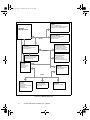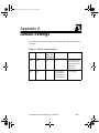
1
net486.book Page i Wednesday, May 26, 1999 12:24 PM
Net486 Demonstration Board
User’s Manual
Order # 22649A
net486.book Page ii Wednesday, May 26, 1999 12:24 PM
Net486 Demonstration Board User’s Manual
© 1999 Advanced Micro Devices, Inc. All rights reserved.
The contents of this document are provided in connection with Advanced Micro Devices, Inc. (“AMD”) products. AMD makes
no representations or warranties with respect to the accuracy or completeness of the contents of this publication and reserves
the right to make changes to specifications and product descriptions at any time without notice. No license, whether express,
implied, arising by estoppel or otherwise, to any intellectual property rights is granted by this publication. Except as set forth
in AMD's Standard Terms and Conditions of Sale, AMD assumes no liability whatsoever, and disclaims any express or implied
warranty, relating to its products including, but not limited to, the implied warranty of merchantability, fitness for a particular
purpose, or infringement of any intellectual property right.
AMD's products are not designed, intended, authorized or warranted for use as components in systems intended for surgical
implant into the body, or in other applications intended to support or sustain life, or in any other application in which the
failure of AMD's product could create a situation where personal injury, death, or severe property or environmental damage
may occur. AMD reserves the right to discontinue or make changes to its products at any time without notice.
NO SUPPORT OBLIGATION: AMD is not obligated to furnish, support, or make any further information, software, technical
information, know-how, or show-how available to you.
AMD, the AMD logo, and combinations thereof, E86, NetPHY, and PCnet are trademarks of, Am486 and PAL are registered trademarks
of, and FusionE86 is a service mark of Advanced Micro Devices, Inc.
Vantis is a trademark of Vantis Corporation.
Windows and Windows NT are registered trademarks of Microsoft Corporation.
Product names used in this publication are for identification purposes only and may be trademarks of their respective companies.
net486.book Page iii Wednesday, May 26, 1999 12:24 PM
IF YOU HAVE QUESTIONS, WE’RE HERE TO HELP YOU.
The AMD customer service network includes U.S. offices, international offices, and a customer
training center. Expert technical assistance is available from the AMD worldwide staff of field
application engineers and factory support staff to answer E86™ family hardware and software
development questions.
Frequently accessed numbers are listed below. Additional contact information is listed on the back
of this manual. AMD’s WWW site lists the latest phone numbers.
Technical Support
Answers to technical questions are available online, through e-mail, and by telephone.
Go to AMD’s home page at www.amd.com and follow the Service link for the latest AMD technical
support phone numbers, software, and Frequently Asked Questions.
For technical support questions on all E86 products, send e-mail to [email protected] (in the
US and Canada) or [email protected] (in Europe and the UK).
You can also call the AMD Corporate Applications Hotline at:
(800) 222-9323
44-(0) 1276-803-299
Toll-free for U.S. and Canada
U.K. and Europe hotline
WWW Support
For specific information on E86 products, access the AMD home page at www.amd.com and follow
the Embedded Processors link. These pages provide information on upcoming product releases,
overviews of existing products, information on product support and tools, and a list of technical
documentation. Support tools include online benchmarking tools and CodeKit software—source code
example applications. Many of the technical documents are available online in PDF form.
Questions, requests, and input concerning AMD’s WWW pages can be sent via e-mail to
[email protected].
Documentation and Literature Support
Data books, user’s manuals, data sheets, application notes, and product CDs are free with a simple
phone call. Internationally, contact your local AMD sales office for product literature.
To order literature, call:
(800) 222-9323
(512) 602-5651
(512) 602-7639
Toll-free for U.S. and Canada
Direct dial worldwide
Fax
Third-Party Support
AMD’s FusionE86SM program partners provide an array of products designed to meet critical time-to-market
needs. Products and solutions available include emulators, hardware and software debuggers, board-level
products, and software development tools, among others. The WWW site and the E86™ Family Products
Development Tools CD, order #21058, describe these solutions. In addition, mature development tools and
applications for the x86 platform are widely available in the general marketplace.
net486.book Page iv Wednesday, May 26, 1999 12:24 PM
net486.book Page v Wednesday, May 26, 1999 12:24 PM
Contents
About the Demonstration Board
Demonstration Board Features ............................................................................ xi
Am486® Microprocessor................................................................................ xi
Core Logic Chipset ......................................................................................... xi
DRAM Main Memory.................................................................................... xii
Boot and EIP Flash Memory.......................................................................... xii
PC and DOS Compatibility............................................................................ xii
PC Peripheral Support................................................................................... xiii
Two Ethernet Controllers .............................................................................. xiii
Industry-Standard Expansion ........................................................................ xiv
Form Factor and Power Supply..................................................................... xiv
BIOS and Software ....................................................................................... xiv
Demonstration Board Documentation.................................................................xv
About This Manual .........................................................................................xv
Suggested Reference Material....................................................................... xvi
Documentation Conventions........................................................................ xvii
Net486 Demonstration Board User’s Manual
v
net486.book Page vi Wednesday, May 26, 1999 12:24 PM
Chapter 1
Quick Start
Setting Up the Board ......................................................................................... 1-2
Installation Requirements.............................................................................. 1-3
Board Installation .......................................................................................... 1-4
Starting from Flash Memory ............................................................................. 1-6
Starting from Floppy Disk ................................................................................. 1-7
Starting from an IDE Hard Disk........................................................................ 1-8
Installation Troubleshooting .............................................................................. 1-9
Chapter 2
Board Functional Description
Feature and Layout Diagrams............................................................................ 2-2
Jumper Functions............................................................................................... 2-6
Board Restrictions ............................................................................................. 2-6
Board Features ................................................................................................... 2-7
Am486® Microprocessor (O15) ................................................................... 2-7
Core Logic Chipset (K15, M5, D12)........................................................... 2-10
Onboard Ethernet Controllers (I19 and G15).............................................. 2-12
Expansion Bus (G10 and P10) .................................................................... 2-13
DRAM Main Memory (F6)......................................................................... 2-14
Boot Flash Memory (M2)............................................................................ 2-15
EIP Flash Memory (K10) ............................................................................ 2-16
Super I/O (I5) .............................................................................................. 2-19
IDE Hard Disk (L1)..................................................................................... 2-22
Keyboard (A10)........................................................................................... 2-22
Power Supply (A2)...................................................................................... 2-23
Reset Switch (O20) ..................................................................................... 2-23
vi
Net486 Demonstration Board User’s Manual
net486.book Page vii Wednesday, May 26, 1999 12:24 PM
Appendix A
Default Settings
Default Settings ................................................................................................ A-1
Appendix B
Bill of Materials
Bill of Materials.................................................................................................B-1
Index
Index ........................................................................................................... Index-1
Net486 Demonstration Board User’s Manual
vii
net486.book Page viii Wednesday, May 26, 1999 2:26 PM
List of Figures
Figure 0-1. Board Overview.................................................................................................... x
Figure 2-1. Board Overview (Same as Figure 0-1) .............................................................. 2-3
Figure 2-2. Board Block Diagram ........................................................................................ 2-4
Figure 2-3. Board Layout ..................................................................................................... 2-5
Figure 2-4. Am486® Microprocessor Block Diagram......................................................... 2-9
Figure 2-5. Typical Memory Map With EIP Flash Memory.............................................. 2-18
Figure 2-6. Serial Port Connector Pins............................................................................... 2-20
Figure 2-7. Parallel Port Socket.......................................................................................... 2-21
List of Tables
Table 0-1.
Notational Conventions
................................................................................ xvii
Table 1-1.
Installation Troubleshooting ............................................................................. 1-9
Table 2-1.
Board Jumper Summary .................................................................................. 2-6
Table 2-2.
PCI Configuration Addressing ....................................................................... 2-10
Table 2-3.
Serial Port Pin/Signal Table ............................................................................ 2-20
Table 2-4.
Parallel Port Pin/Signal Table.......................................................................... 2-21
Table 2-5.
Switch Summary.............................................................................................. 2-23
Table A-1.
Default Jumper Settings.................................................................................... A-1
viii
Net486 Demonstration Board User’s Manual
net486.book Page ix Wednesday, May 26, 1999 12:24 PM
About the Demonstration Board
Congratulations on your decision to design with the Am486® microprocessor. The
Net486 demonstration board provides a single-board demonstration of an
embedded Am486 microprocessor-based communication controller with two
onboard 10- or 100-Mbit/s Ethernet controllers and a PC/104-Plus expansion bus.
The Net486 demonstration board includes 8.5 Mbytes of Flash memory, a PC/104Plus connector with access to both PCI and ISA buses, and standard PC peripherals.
In addition, the platform’s compact, targeted design makes it suitable for
demonstrating customer designs in a sales environment.
Refer to the Am486 microprocessor documentation (listed on page xvi) for detailed
information on the Am486 microprocessor.
Figure 0-1 on page x provides an overview of the Net486 demonstration board’s
features.
Net486 Demonstration Board User’s Manual
ix
net486.book Page x Wednesday, May 26, 1999 12:24 PM
DRAM
One 72-pin SIMM Socket
Supports 32 Mbytes of EDO or FPM DRAM
32 Mbytes of 60-ns DRAM Installed
Am486®
Microprocessor
EIP Flash Memory
Addressed as fourth DRAM bank
8-Mbyte Flash Memory
Fast Read Access
CPU Bus
PCnet™-Fast+
Ethernet Controller
ALi M1489
Memory, and DRAM Controller
(Northbridge Chip)
PCI Bus
Am79C972 Device Included
(Am79C973 Device Supported)
10/100Base-T Port (RJ-45)
Three Connection Status LEDs
PCnet™-Home
Ethernet Controller
IDE Interface
Am79C978 Device
10Base-T Port (RJ-45)
HomePNA Port (RJ-11)
Three Connection Status LEDs
2-mm-Pitch Ribbon Connector
Supports up to Two Devices
Connector Status LED
ALi M1487
ISA Bridge
(Southbridge Chip)
PCI Bus Arbiter
Reset Switch
PC/104 Plus
Expansion
Compact Stacked Interface
PCI and ISA Buses
ISA Bus
ALi M5113A
Super I/O
IrDA Module
2 Serial Interfaces
(one DB-9, one 10-pin header)
1 Parallel Port
Floppy Disk Interface
Boot FlashSocket
32-pin PLCC Package
Up to 512K x8 Supported
BIOS Included
Figure 0-1. Board Overview
x
Net486 Demonstration Board User’s Manual
M5042 Keyboard
Controller
AT Keyboard Controller
net486.book Page xi Wednesday, May 26, 1999 12:24 PM
Demonstration Board Features
This section describes the following features of the Net486 demonstration board:
•
•
•
•
•
•
•
•
•
•
“Am486® Microprocessor” on page xi
“Core Logic Chipset” on page xi
“DRAM Main Memory” on page xii
“Boot and EIP Flash Memory” on page xii
“PC and DOS Compatibility” on page xii
“PC Peripheral Support” on page xiii
“Two Ethernet Controllers” on page xiii
“Industry-Standard Expansion” on page xiv
“Form Factor and Power Supply” on page xiv
“BIOS and Software” on page xiv
Am486® Microprocessor
• 133 MHz AMD Am486DX5 microprocessor is included.
• Factory option to use 100 MHz Am486DX4 microprocessor.
• 208-pin low-cost SQFP package with internal heat spreader.
Core Logic Chipset
• Acer Labs FINALi 486 PCI chipset
– M1489 Northbridge cache, memory, and PCI controller
– M1487 Southbridge ISA bus controller
– M5042 mouse/keyboard controller
Net486 Demonstration Board User’s Manual
xi
net486.book Page xii Wednesday, May 26, 1999 12:24 PM
DRAM Main Memory
• Supports one bank of 32- or 36-bit-wide, 16-Mbit technology DRAM using an
industry-standard 5-V 72-pin SIMM. DRAM can be fast page mode (FPM) or
extended data out (EDO).
• 32 Mbyte of 60-ns EDO DRAM SIMM installed in the provided slot.
• DRAM is accessible by CPU and PCI bus masters.
• L1 cache snoop cycles are generated for PCI master memory accesses.
Boot and EIP Flash Memory
• 32-pin PLCC boot Flash memory socket addressed at the reset vector. 512-Kbyte
x8 boot Flash BIOS is included.
• 8-Mbyte Flash memory for execute-in-place (EIP) applications, located on the
memory bus in place of one DRAM bank. EIP Flash is implemented using an
AMD 22V10 PAL® device for glue logic.
PC and DOS Compatibility
• Off-the-shelf PC chipset provides common I/O functions found in a PC:
- Two 82C59-compatible interrupt controllers
- One 82C54-compatible programmable interval timer
- Two 82C37-compatible DMA controllers (seven channels)
- DS1287-compatible real-time clock (RTC)
xii
Net486 Demonstration Board User’s Manual
net486.book Page xiii Wednesday, May 26, 1999 12:24 PM
PC Peripheral Support
• One IDE connector with LED (interface provided by chipset’s M1489 device).
• M5113A super I/O device functions:
– Two 16550-compatible serial ports.
– One parallel port with Error and Ready status LEDs. Supports Centronics,
bidirectional, enhanced parallel port (EPP), and extended capabilities port
(ECP) interfaces.
– IrDA port (115 Kbyte/s).
– Floppy disk interface.
• PC/AT keyboard connector (interface provided by M5042 device).
Two Ethernet Controllers
• AMD PCnet™-Fast+ Ethernet controller chip, Am79C972.
– External PHY transceiver supports full duplex
– Design supports alternative Am79C973 controller with internal transceiver.
– RJ-45 connector for operation at 10 or 100 Mbit/s.
• AMD PCnet™-Home Ethernet controller chip, Am79C978.
– Internal PHY transceiver supports full duplex.
– RJ-45 connector for 10 Mbit/s operation.
– Two RJ-11 connectors for 1 Mbit/s Home Phoneline Networking Alliance
(HomePNA) operation.
• Features supported by both onboard Ethernet controllers:
– 32-bit PCI bus interface with bus mastering capability.
– Integrated 12-Kbyte buffer.
– Preprogrammed 1-Kbyte serial EEPROM included for Ethernet
configuration.
– IEEE802.3 and NetPC compliance.
– LED indicators for transmit activity, receive activity, and link speed.
Net486 Demonstration Board User’s Manual
xiii
net486.book Page xiv Wednesday, May 26, 1999 12:24 PM
Industry-Standard Expansion
• PC/104-Plus connector.
Form Factor and Power Supply
• Compact 5 x 7” form factor with connectors and LEDs placed for convenient
demonstration.
• Power provided by a single, 12-V power supply.
BIOS and Software
The included diskette or CD-ROM contains information about the included BIOS
and any additional utility and demonstration software for the Net486 demonstration
board.
xiv
Net486 Demonstration Board User’s Manual
net486.book Page xv Wednesday, May 26, 1999 12:24 PM
Demonstration Board Documentation
The Net486 Demonstration Board User’s Manual provides information on the
design and function of the development platform. The software shipped with the
board is described in the README files and online BIOS manual included with
your kit.
The included online documentation is in either text or Adobe Acrobat (PDF)
format. The latest Acrobat Reader is available from Adobe’s site on the World
Wide Web (currently at www.adobe.com).
About This Manual
Chapter 1, “Quick Start” helps you quickly set up and start using the demonstration
board.
Chapter 2, “Board Functional Description” contains descriptions of the basic
sections of the board: layout, microprocessor, core logic chipset, Ethernet controller,
DRAM, boot and Flash memory, PC/104-Plus bus interface, super I/O, hard disk,
keyboard, IDE interface, power, and switches.
Appendix A, “Default Settings” summarizes the jumper positions on the board when
it is shipped.
Appendix B, “Bill of Materials” shows the bill of materials for the board, and the
actual CAD schematics used to build the board.
An index is also included.
Net486 Demonstration Board User’s Manual
xv
net486.book Page xvi Wednesday, May 26, 1999 12:24 PM
Suggested Reference Material
The following AMD documentation may be of interest to the Net486 demonstration
board user. For information on ordering literature, see page iii.
• Enhanced Am486®DX Microprocessor Family Data Sheet, order #20736
• Am486®DX/DX2 Microprocessor Hardware Reference Manual, order #17965
• Am486® Microprocessor Software User’s Manual, order #18497
• Am79C972 PCnet™-FAST+ Enhanced 10/100 Mbps PCI Ethernet Controller
with OnNow Support Data Sheet, order #21485
• Am79C972 PCnet™-Home Single-Chip 1/10 Mbps PCI Home Networking
Controller Data Sheet, order #22206
• E86 Family Products Development Tools CD, order #21058
• Flash Memory Products Data Book, order #11796
For current application notes and technical bulletins, see our World Wide Web page
at www.amd.com.
The following non-AMD documents are also recommended:
• FINALi 486 M1489/1487 PCI Chip Set Preliminary Data Sheet
Acer Laboratories Inc. See www.acerlabs.com for contact information. Related
BIOS guidelines, errata, and application documents are also available.
• M5113: Enhanced Super I/O Controller Data Sheet
Acer Laboratories Inc. See www.acerlabs.com for contact information.
xvi
Net486 Demonstration Board User’s Manual
net486.book Page xvii Wednesday, May 26, 1999 12:24 PM
Documentation Conventions
The Advanced Micro Devices Net486 Demonstration Board User’s Manual uses
the conventions shown in Table 0-1 (unless otherwise noted). These same
conventions are used in all the E86™ family support product manuals.
Table 0-1. Notational Conventions
Symbol
Usage
Boldface
Indicates that characters must be entered
exactly as shown, except that the alphabetic case is
only significant when indicated.
Italic
Indicates a descriptive term to be replaced with a
user-specified term.
Typewriter face
Indicates computer text input or output in an example
or listing.
Net486 Demonstration Board User’s Manual
xvii
net486.book Page xviii Wednesday, May 26, 1999 12:24 PM
xviii
Net486 Demonstration Board User’s Manual
net486.book Page 1 Wednesday, May 26, 1999 12:24 PM
Chapter 1
Quick Start
This chapter provides information that helps you quickly set up and start using the
Net486 demonstration board (Net486 demonstration board).
The Net486 demonstration board is shipped with a BIOS that has been configured
specifically for the chipset used on this platform. The BIOS contains the code that
enables the Net486 demonstration board to function as a standard AT-compatible
PC, using an AT-compatible keyboard and display and a PC/104-Plus-compatible
VGA display adapter.
The included BIOS software also supports redirection of the command-line console
to the serial port and configuration of onboard Flash memory as a resident flash
disk (RFD) that can also be set up as a boot device. See the online BIOS manual
included with your kit for information about booting from an RFD.
Details on the included BIOS can be found in the online BIOS documentation
shipped with your kit.
The Net486 demonstration board can run AT-compatible operating system
software. You can start the system from Flash memory (if so configured), from a
bootable floppy disk, or from an attached IDE hard disk drive that already has the
operating system installed.
For information on how to:
• Set up the Net486 demonstration board, see page 1-2.
• Boot the Net486 demonstration board from Flash memory, see page 1-6.
• Boot the Net486 demonstration board from a floppy disk, see page 1-7.
• Boot the Net486 demonstration board from a hard disk, see page 1-8.
• Troubleshoot installation problems, see page 1-9.
Net486 Demonstration Board User’s Manual
1-1
net486.book Page 2 Wednesday, May 26, 1999 12:24 PM
Setting Up the Board
!
CAUTION: As with all computer equipment, the Net486
demonstration board may be damaged by electrostatic
discharge (ESD). Please take proper ESD precautions when
handling any board.
Warning: Read before using this board
Before applying power, the following precautions should be taken to avoid damage
or misuse of the board:
• Make sure the provided power supply is plugged into the board’s power
connector correctly. See “Power Supply (A2)” on page 2-23 for details.
• See Figure 2-3 on page 2-5 for connector positions.
• Check the floppy disk or CD-ROM that was shipped with your kit for README
or errata documentation. Read all the information carefully before continuing.
For current application notes and technical bulletins, see the AMD World Wide
Web page at www.amd.com and follow the link to Embedded Systems.
1-2
Net486 Demonstration Board User’s Manual
net486.book Page 3 Wednesday, May 26, 1999 12:24 PM
Installation Requirements
You need to provide the following items (in addition to the board from the kit).
Required for redirected-console operation:
• An ANSI terminal or a PC running ANSI terminal emulation software
• A null-modem cable
Required for stand-alone operation:
• A VGA-compatible monitor
• A PC/104-Plus video card that supports VGA
• A cable to connect the monitor to the video card
• An AT-compatible keyboard
To boot from a floppy disk:
• An AT-compatible floppy disk drive
• A bootable DOS floppy disk
• A compact (notebook-style) floppy disk ribbon cable. You also need a ribbon
cable adapter if the floppy disk drive requires a 0.1-inch-pitch connector.
To boot from a hard disk:
• An IDE-compatible hard disk drive
• AT-compatible operating system (preinstalled on the hard disk drive)
• A compact (notebook-style) 44-pin 2-mm-pitch hard-disk-drive cable. You also
need a cable adapter if your hard disk drive requires a 0.1-inch-pitch connector.
Only one boot disk image (Flash memory, floppy disk, or hard disk) is required.
For example, you can boot from a floppy disk to configure a resident flash disk
and install the operating system, and then start from Flash memory from then on.
!
CAUTION: Use the configuration described here when you first start
the Net486 demonstration board. Before using other features, read the
appropriate sections in Chapter 2, “Board Functional Description.”
The combined +5 V current requirement for disk drives and expansion
devices must not exceed 1.1 A. See “Power Budget” on page 2-13.
Net486 Demonstration Board User’s Manual
1-3
net486.book Page 4 Wednesday, May 26, 1999 12:24 PM
Board Installation
NOTE: See Figure 2-2 on page 2-4 for a block diagram of the board. See Figure
2-3 on page 2-5 for a layout diagram of the board, including connector locations
referenced in this section.
!
DANGER: Make sure the power supply and the VGA
monitor are not plugged into an electrical outlet during
the following steps.
1. Remove the board from the shipping carton. Visually inspect the board to verify
that it was not damaged during shipment. The following steps assume the
board’s jumpers are in the factory default configuration (settings are listed in
Appendix A, “Default Settings”).
2. If you are installing a floppy disk drive, perform the following steps:
a. Inspect the 34-lead, floppy-disk-drive ribbon cable that you are providing.
Note the contacts (metallic pads) of the cable end.
b. Connect one end of the ribbon cable to the ribbon connector (connector J12
at location H1) on the Net486 demonstration board. Orient the ribbon so
its contacts are facing the edge of the board. Lift the clamping bar on the
board connector; slide in the ribbon; then press the clamping bar down again
to secure the ribbon.
c. Connect the other end of the ribbon cable to the floppy disk drive. The
connector’s orientation should be indicated in the drive documentation, or
marked near the connector on the drive.
3. If you are installing a hard disk drive, perform the following steps:
a. Inspect the 44-wire IDE ribbon cable that you are providing. Note the red
wire or any other marking that indicates wire 1 on the cable.
b. Connect one end of the 44-wire IDE cable to the hard disk drive. The
connector’s orientation should be indicated in the drive documentation, or
marked near the connector on the drive. Usually wire 1 is oriented towards
the drive’s power cable connector.
c. Connect the other end of the 44-wire IDE cable to the 44-pin connector
(connector J14 at location M1) on the Net486 demonstration board (with
wire 1 oriented towards the floppy disk drive connector).
1-4
Net486 Demonstration Board User’s Manual
net486.book Page 5 Wednesday, May 26, 1999 12:24 PM
4. If you are setting up for redirected-console operation, connect the null-modem
cable that you provided between the COM1 connector on the Net486
demonstration board (connector J6 at location A7) and the appropriate serial
port of your terminal or PC.
5. If you are setting up for stand-alone operation, perform the following steps:
a. Insert a PC/104-Plus VGA-compatible video card into the PC/104-Plus
headers (parts J11, J15 and J16 at locations G10 and P10)
b. Connect the monitor cable from the monitor to the D-connector on the video
card just as you would for a standard PC.
c. Connect the AT keyboard to the keyboard connector (connector J5 at
location A10).
6. Connect the +12 V DC output cable from the provided AC adapter to the +12-V
power connector on the Net486 demonstration board (part J8 at location A2).
!
CAUTION: Failure to use the correct AC adapter can damage
the Net486 demonstration board.
The combined +5 V current requirement for disk drives and expansion
devices must not exceed 1.1 A. See “Power Budget” on page 2-13.
Net486 Demonstration Board User’s Manual
1-5
net486.book Page 6 Wednesday, May 26, 1999 12:24 PM
Starting from Flash Memory
NOTE: See the online documentation for the included BIOS if your Net486
demonstration board does not already have a resident flash disk (RFD) configured
and an operating system installed. The operating system used must be able to
operate entirely within a command-line console environment.
Use the following steps to start the Net486 demonstration board from a resident
flash disk using console redirection:
1. Make sure you have installed the Net486 demonstration board correctly as
described in “Setting Up the Board” on page 1-2.
2. Configure your ANSI terminal or terminal emulation software with the
following settings:
–
–
–
–
9600 bits/s
8 data bits
No parity
1 stop bit
3. Plug in the AC adapter.
4. Turn on the power switch (part S1 at location A4).
The power LED should light. The speaker should beep and the terminal should
start displaying startup information.
5. The first time you start the system, the BIOS might display a message reporting
a CMOS error or some other BIOS configuration problem. Follow the
instructions shown on the screen to enter the Setup utility. Once you are in the
Setup utility, you can set the system’s date, time, startup drive, and other
options.
The BIOS setup utility is also used to configure and format the RFD before
installing an operating system in Flash memory.
For more information on the included BIOS, see the online BIOS manual
included with your kit.
6. The system should now boot from the DOS RFD just like a standard PC. If you
encounter any problems, see “Installation Troubleshooting” on page 1-9.
1-6
Net486 Demonstration Board User’s Manual
net486.book Page 7 Wednesday, May 26, 1999 12:24 PM
Starting from Floppy Disk
Use the following steps to start the Net486 demonstration board from a bootable
floppy disk:
1. Make sure you have installed the Net486 demonstration board correctly as
described in “Setting Up the Board” on page 1-2.
2. Plug the VGA monitor into an electrical outlet and turn it on.
3. Plug in the AC adapter.
4. Insert a bootable DOS floppy disk (not included) in the disk drive.
5. Turn on the power switch (part S1 at location A4).
The power LED should light. The speaker should beep and the monitor should
start displaying startup information.
6. The first time you start the system, the BIOS might display a message reporting
a CMOS error or some other BIOS configuration problem. Follow the
instructions shown on the screen to enter the Setup utility. Once you are in the
Setup utility, you can set the system’s date, time, startup drive, and other
options.
The BIOS setup utility is also used to configure and format a resident flash disk
(RFD) before installing an operating system in Flash memory.
For more information on the included BIOS, see the online BIOS manual
included with your kit.
7. Save and exit the setup utility.
8. The system should now boot from the DOS floppy disk just like a standard PC.
If you encounter any problems, see “Installation Troubleshooting” on page 1-9.
Net486 Demonstration Board User’s Manual
1-7
net486.book Page 8 Wednesday, May 26, 1999 12:24 PM
Starting from an IDE Hard Disk
Use the following steps to start up the Net486 demonstration board from an IDE
hard disk on which you have preinstalled an operating system (while it was
connected to another PC):
1. Make sure you have installed the Net486 demonstration board correctly as
described in “Setting Up the Board” on page 1-2.
2. Plug the VGA monitor into an electrical outlet and turn it on.
3. Plug in the AC adapter.
4. If a floppy disk drive is installed, make sure it is empty.
5. Turn on the power switch (part S1 at location A4).
The power LED should light. The speaker should beep and the monitor should
start displaying startup information.
6. The first time you start the system, the BIOS might display a message reporting
a CMOS error or some other BIOS configuration problem. Follow the
instructions shown on the screen to enter the Setup utility. Once you are in the
Setup utility, you can set the system’s date, time, startup drive, and other options.
7. In the BIOS setup utility, use the automatic configuration option to set up
Drive C. Select either physical addressing or logical block addressing (LBA)
as appropriate for your hard disk drive.
The BIOS setup utility is also used to configure and format a resident flash disk
(RFD) before installing an operating system in Flash memory.
For more information on the included BIOS, see the online BIOS manual
included with your kit.
8. Save and exit the setup utility.
9. The system should now boot using the operating system on the hard disk. If
you encounter any problems, see “Installation Troubleshooting” on page 1-9.
1-8
Net486 Demonstration Board User’s Manual
net486.book Page 9 Wednesday, May 26, 1999 12:24 PM
Installation Troubleshooting
Table 1-1. Installation Troubleshooting
Problem
Solution
The power LED does not light
after I turn on the power switch.
Make sure the correct AC power adapter is plugged in
and correctly attached to the board.
I see nothing on the display and do
not hear any beeps from the
speaker. I do not hear the head
synchronization on the floppy disk
drive (if attached).
Ensure processor reset by pressing the Reset button (part
S2 at location P20).
Check that the BIOS Flash memory is correctly installed
in its socket (part U27 at location M2).
Make sure all cables are connected properly, all adapters
are seated firmly in their slots, and the CMOS battery is
correctly installed.
If the problem persists, invalidate the CMOS RAM by
temporarily moving jumper W1 from pins 1–2 to connect
pins 2–3; wait a few seconds, then move the jumper back
to pins 1–2. This makes it necessary to run the Setup
utility and restore startup settings, but it also clears any
corrupted settings that might be present.
I am using a redirected console. I
hear a beep on the speaker but see
nothing on my terminal screen.
Make sure your terminal or terminal emulator supports
ANSI and is configured correctly (8, N, 1, 9600 baud).
Make sure you are using a null-modem cable and that the
cable is connected to the correct port on your terminal and
to the Net486 demonstration board’s COM1 port (part J6
at location A0).
I am using a stand-alone
installation. I hear a beep on the
speaker but see nothing on the
VGA monitor.
Check that the monitor is plugged in and turned on, that
it is correctly connected to the video card, and that the
video card is correctly seated in the connectors.
Check that the video card supports VGA.
Net486 Demonstration Board User’s Manual
1-9
net486.book Page 10 Wednesday, May 26, 1999 12:24 PM
Table 1-1. Installation Troubleshooting (Continued)
Problem
Solution
I see the startup information on the
monitor but the memory test stops
at an incorrect memory size
(1 Mbyte equals 1024 Kbyte).
Make sure the SIMM that came with the kit is securely
installed in the SIMM socket.
I see the startup information on the
monitor but it says there’s a battery
problem or CMOS checksum
error and the system doesn’t finish
booting.
Follow the BIOS instructions to run the Setup utility to
configure the CMOS RAM and save settings.
I configured the CMOS RAM and
saved my settings, but settings are
lost the next time I turn on the
Net486 demonstration board.
Make sure a fresh 3.0-V 20-mm coin cell is installed
correctly (“+” side facing up) in the BT1 battery holder
at location L19.
I don’t hear any sound from the
floppy disk drive and the system
does not boot from a floppy disk.
Check that the ribbon cable to the floppy disk drive is
properly connected at both the drive end and the board
end (board connector J12 at location H1). Check the drive
documentation to verify which side of the ribbon is lead 1,
and orient that lead towards the front of the board.
Check that the CMOS setup indicates that drive A is the
correct size and capacity for your floppy disk drive.
I hear the floppy disk being
accessed but get an error message
“Non System disk” or “Drive A
not found.”
Check that the floppy disk in the drive is bootable, just as
you would on a standard PC.
Make sure the floppy disk drive is connected properly.
In the BIOS setup utility, make sure the BIOS is
configured to boot from floppy disk, and that the floppy
disk size and density is configured properly.
I get a “Missing Keyboard” error
message on the monitor during
boot-up.
Check that an AT-style keyboard is properly connected.
The BIOS debugging monitor
prompt is displayed.
Check that the DRAM and any PC/104-Plus devices are
installed correctly and known to be functional.
1-10
Net486 Demonstration Board User’s Manual
net486.book Page 11 Wednesday, May 26, 1999 12:24 PM
Table 1-1. Installation Troubleshooting (Continued)
Problem
Solution
I have installed a hard disk with a
preinstalled operating system, but
the Net486 demonstration board
won’t access the hard disk.
Check that the 44-wire IDE cable is properly connected
at both the drive end and the board end (board connector
J14 at location M1). Check that the CMOS setup is
configured correctly for your drive.
Make sure the board will start from a bootable floppy disk
in drive A. Then try to do a directory listing of drive C.
If the directory listing of C works, the drive is functioning
and there is a problem with the drive’s boot block or
system image. (Note that some operating systems will
display an error if you list an empty directory. If this
happens, try copying a file to the drive; then do a directory
listing again. If this fails, check the drive for boot block
viruses.)
Make sure the drive functions properly on a different
system.
There is a problem you cannot
resolve.
Check that the board is set to its default settings (see
Appendix A, “Default Settings”).
Contact the AMD Technical Support Hotline
(see page iii).
Net486 Demonstration Board User’s Manual
1-11
net486.book Page 12 Wednesday, May 26, 1999 12:24 PM
1-12
Net486 Demonstration Board User’s Manual
net486.book Page 1 Wednesday, May 26, 1999 12:24 PM
Chapter 2
Board Functional Description
The Net486 demonstration board provides a compact demonstration system for
Am486 microprocessor-based designs. Read the following sections to learn more
about the board:
•
•
•
•
“Feature and Layout Diagrams” on page 2-2
“Jumper Functions” on page 2-6
“Board Restrictions” on page 2-6
“Board Features” on page 2-7
–
–
–
–
–
–
–
–
–
–
–
–
“Am486® Microprocessor (O15)” on page 2-7
“Core Logic Chipset (K15, M5, D12)” on page 2-10
“Onboard Ethernet Controllers (I19 and G15)” on page 2-12
“Expansion Bus (G10 and P10)” on page 2-13
“DRAM Main Memory (F6)” on page 2-14
“Boot Flash Memory (M2)” on page 2-15
“EIP Flash Memory (K10)” on page 2-16
“Super I/O (I5)” on page 2-19
- “IrDA Interface (Q19)” on page 2-19
- “Floppy Disk Drive (E20)” on page 2-19
- “Serial Ports (A7 and K2)” on page 2-20
- “Parallel Port (H2)” on page 2-21
“IDE Hard Disk (L1)” on page 2-22
“Keyboard (A10)” on page 2-22
“Power Supply (A2)” on page 2-23
“Reset Switch (O20)” on page 2-23
See the appendices for information about default board settings and bill of
materials. Schematics for the Net486 demonstration board are provided in a
separate document.
Net486 Demonstration Board User’s Manual
2-1
net486.book Page 2 Wednesday, May 26, 1999 12:24 PM
Feature and Layout Diagrams
The following figures summarize the features and layout of the Net486
demonstration board.
• Figure 2-1 on page 2-3 provides an overview of the board’s features.
• Figure 2-2 on page 2-4 is the block diagram for the board.
• Figure 2-3 on page 2-5 shows the board layout and component locations.
2-2
Net486 Demonstration Board User’s Manual
net486.book Page 3 Wednesday, May 26, 1999 12:24 PM
DRAM
One 72-pin SIMM Socket
Supports 32 Mbytes of EDO or FPM DRAM
32 Mbytes of 60-ns DRAM Installed
Am486®
Microprocessor
EIP Flash Memory
Addressed as fourth DRAM bank
8-Mbyte Flash Memory
Fast Read Access
CPU Bus
PCnet™-Fast+
Ethernet Controller
ALi M1489
Memory, and DRAM Controller
(Northbridge Chip)
PCI Bus
Am79C972 Device Included
(Am79C973 Device Supported)
10/100Base-T Port (RJ-45)
Three Connection Status LEDs
PCnet™-Home
Ethernet Controller
IDE Interface
Am79C978 Device
10Base-T Port (RJ-45)
HomePNA Port (RJ-11)
Three Connection Status LEDs
2-mm-Pitch Ribbon Connector
Supports up to Two Devices
Connector Status LED
ALi M1487
ISA Bridge
(Southbridge Chip)
PCI Bus Arbiter
Reset Switch
PC/104 Plus
Expansion
Compact Stacked Interface
PCI and ISA Buses
ISA Bus
ALi M5113A
Super I/O
Boot FlashSocket
IrDA Module
2 Serial Interfaces
(one DB-9, one 10-pin header)
1 Parallel Port
Floppy Disk Interface
32-pin PLCC Package
Up to 512K x8 Supported
BIOS Included
M5042 Keyboard
Controller
AT Keyboard Controller
Figure 2-1. Board Overview (Same as Figure 0-1)
Net486 Demonstration Board User’s Manual
2-3
net486.book Page 4 Wednesday, May 26, 1999 12:24 PM
CPU Bus
Am486®
CPU
Buffer
ALi M1489
Northbridge
CPU
Clock
5V
Regulator
IDE Conn.
32 Mbyte
DRAM
PCI Bus
PCnet™-FAST+
Ethernet
NetPHY™
Device
RJ-45 Conn.
RJ-45 Conn.
3.3 V
Regulator
PCnet™-Home
Ethernet
RJ-11 Conn.
PC/104-Plus
Connector
+12 V
Power
Conn.
ALi M1487
Southbridge
ISA Bus
ALi M5113
Super I/O
Speaker
Boot Flash
Memory
COM1
Conn.
Serial
Translator
IrDA
LEDs
COM2
Header
Serial
Translator
Parallel
Header
Figure 2-2. Board Block Diagram
2-4
8 Mbyte
Flash
Memory
PAL®
Device
Net486 Demonstration Board User’s Manual
ALi M5042
Keyboard
Controller
Keyboard
Conn.
net486.book Page 5 Wednesday, May 26, 1999 12:24 PM
A
B
C
D
E
F
G
H
I
J
K
L
M
N
O
P
Q
Pin 1
1
2
+12 V
Conn.
Parallel Port
Pin 1
Pin 1
1
IDE Hard Disk Conn.
Pin 1
Floppy Disk Conn.
COM2
Power/
Status
LEDs
BIOS
3
On/
Off
4
3
4
M5113
Super I/O
5
5
M1487
DRAM
SIMM
6
7
2
6
Southbridge
7
PAL®
Logic
COM1
8
8
9
9
10
PC/104
Plus
PCI
KBD
PC/104
Plus
ISA
EIP
Flash
Memory
11
10
11
M5042
KBD
12
12
1 Mbit/s
HomePNA
Conn.
13
14
13
14
1 Mbit/s
HomePNA
Conn.
15
Am79C978
PCnet™-Home
Controller
Boot
16
10 Mbit/s
ROM
Ethernet
Conn.
15
Am486®
Microprocessor
M1489
Northbridge
16
17
17
18
10/100 Mbit/s
Ethernet
Conn.
19
Am79C972
or
Am79C973
PCnet™-Fast
Controller
Am79C873
NetPHY™
18
IrDA
Speaker
Battery
20
19
20
Reset
A
B
C
D
E
F
G
H
I
J
K
L
M
N
O
P
Q
Figure 2-3. Board Layout
Net486 Demonstration Board User’s Manual
2-5
net486.book Page 6 Wednesday, May 26, 1999 12:24 PM
Jumper Functions
Table 2-1 describes the configuration jumpers on the Net486 demonstration board.
Table 2-1. Board Jumper Summary
Part
Signal
Description
Location in See
Figure 2-3 Schematics*
on Page 2-5 on
W1
VBAT
Used to invalidate the CMOS RAM for
test purposes.
K20
Sheet 7
W2
PPE
Used to assert the parallel port’s PPE
signal. This jumper is ignored by the
included BIOS, but custom
initialization software can interpret this
signal as a user startup option.
K3
Sheet 14
*Schematics are provided in a separate document in your kit.
Board Restrictions
• Using a PCI chipset with the Am486 microprocessor is a fast and effective way
to design a working system, but the system’s features can be limited by the
chipset’s capabilities.
• The chipset does not directly support ROM or Flash memory devices except for
the boot memory. It is possible to implement Flash memory on the DRAM bus
(as in this design’s EIP Flash memory), or on the PCI or ISA bus, but the chipset
only allows booting from the boot memory.
• The Net486 demonstration board implements two banks of execute-in-place
(EIP) Flash memory in place of one DRAM bank. Flash memory timing
requirements limit the chipset’s DRAM interface to its Fast (not Fastest) speed
when the Flash memory is used. This is equivalent to using 70-ns fast-pagemode (FPM) DRAM.
2-6
Net486 Demonstration Board User’s Manual
net486.book Page 7 Wednesday, May 26, 1999 12:24 PM
• The ISA peripherals provided by the M1487 chip are configured for standard
PC-AT compatibility, so there is not much flexibility in assigning interrupts and
DMA channels.
• The Net486 demonstration board does not implement OnNow or Advanced
Configuration and Power Interface (ACPI) power management.
Board Features
The remainder of this chapter describes the features of the Net486 demonstration
board. The number in parentheses following each heading indicates the part’s
location in Figure 2-3 on page 2-5. In addition, other locations mentioned can be
found in the figure. Part numbers mentioned refer to the part reference numbers in
the bill of materials and schematics. See Appendix B, “Bill of Materials”.
Am486® Microprocessor (O15)
The Net486 demonstration board includes an Am486 microprocessor in a 168-pin,
pin-grid-array package (part U31). A CPU heat sink is provided for cooling.
The Enhanced Am486DX Microprocessor Family boosts system performance by
incorporating a 16-Kbyte cache to the existing flexible clock control and enhanced
System Management mode (SMM) features of a 486 CPU. The Enhanced
Am486DX Microprocessor Family has the following characteristics:
• Industry-standard write-back cache support
• Frequent instructions execute in one clock
• 105.6-million bytes/second burst bus at 33 MHz
• Flexible write-through and write-back address control
• Advanced 0.35-µ CMOS-process technology
• 3.3-V or 3.45-V core with 5-V tolerant I/O
• Dynamic data bus sizing for 8-, 16-, and 32-bit buses (the Net486 demonstration
board uses a 32-bit data bus)
• 32-bit address bus
• 32-bit registers
• Supports “soft reset” capability
Net486 Demonstration Board User’s Manual
2-7
net486.book Page 8 Wednesday, May 26, 1999 12:24 PM
• 16-Kbyte unified code and data cache
– Four-way set-associative
– Write-through or write-back policy (the board uses write-back policy by
default)
• Floating-point unit
• Paged, virtual memory management
• Stop clock control for reduced power consumption
• Industry-standard two-pin System Management Interrupt (SMI) for power
management independent of processor operating mode and operating system
• Static design with Auto Halt power-down support
• Wide range of chipsets supporting SMM available to allow product
differentiation (the Net486 demonstration board uses the Acer Laboratories Inc.
FINALi 486 chipset)
• Support available through the AMD FusionE86SM program
2-8
Net486 Demonstration Board User’s Manual
net486.book Page 9 Wednesday, May 26, 1999 12:24 PM
VOLDET
Power
Plane
32-Bit Data Bus
Clock
Interface
32-Bit Data Bus
Clock
Generator
32-Bit Linear Address
Barrel Shifter
Register File
Descriptor
Registers
24
Physical
Address
ALU
Limit and
Attribute
PLA
Cache Unit
2
32
Paging Unit
24
Translation
Lookaside
Buffer
Physical
Address
16-Kbyte
Cache
Prefetcher
32
Micro-instruction
Code
Stream
Floating
Point
Unit
Floating
Point
Register
File
Central and
Protection
Test Unit
Control
ROM
Instruction
Decode
Address
Drivers
Write
Buffers
4x32
Writeback
Buffers
4x32
32
Data Bus
Transceivers
32-Byte
Code Queue
2x16 Bytes
24
A31–A2
BE3–BE0
Copyback
Buffers
4x32
128
Displacement Bus
CLK
CLKMUL
STPCLK
Bus Interface
PCD, PWT
Segmentation
Unit
VCC, VSS
Bus Control
Request
Sequencer
Decoded
Instruction
Path
D31–D0
ADS, W/R, D/C,
M/IO, PCD, PWT,
RDY, LOCK,
PLOCK, BOFF,
A20M, BREQ,
HOLD, HLDA,
RESET, INTR,
NMI, FERR, UP,
IGNNE, SMI,
SMIACT, SRESET
Burst Bus
Control
BRDY, BLAST
Bus Size
Control
BS16, BS8
Cache
Control
Parity
Generation
and Control
JTAG
KEN, FLUSH,
AHOLD, CACHE,
EADS, INV,
WB/WT, HITM
PCHK,
DP3–DP0
TDI, TCK,
TDO, TMS
Figure 2-4. Am486® Microprocessor Block Diagram
Net486 Demonstration Board User’s Manual
2-9
net486.book Page 10 Wednesday, May 26, 1999 12:24 PM
Core Logic Chipset (K15, M5, D12)
The Net486 demonstration board uses the Acer Laboratories Inc. FINALi 486
chipset. The chipset consists of two very-large-scale-integration (VLSI) devices
that provide bus interface and peripheral functions used in the system, plus an
M5042 keyboard controller. See “Keyboard (A10)” on page 2-22.
The M1489 cache, memory, and PCI controller (often called a Northbridge chip)
interfaces the Am486 microprocessor to the memory and PCI bus. The M1489
(part U26 at location K15) performs the following functions:
• Controls DRAM accesses and refresh cycles. See “DRAM Main Memory (F6)”
on page 2-14.
• Provides a 33-MHz, PCI 2.0-compliant interface with 5-V signaling. See
“Expansion Bus (G10 and P10)” on page 2-13.
• Maintains level-1 and level-2 cache coherency for PCI-master-initiated memory
cycles. (Level-2 cache is not implemented in this design.)
• Provides an IDE controller for a hard disk drive. See “IDE Hard Disk (L1)” on
page 2-22.
The Net486 demonstration board routes six PCI address signals via series resistors
to the IDSEL pins on the PC/104-Plus PCI connector and the onboard Ethernet
controllers. The chipset asserts one of these signals to configure each device
according to the device number written to the chipset’s configuration address
register. Table 2-2 relates each device to its device number and signal routing.
Table 2-2. PCI Configuration Addressing
PCI Device
Device
Number
Address
Signal
ID Select
Signal
See
Schematics* on
Am79C972 Ethernet
Device 5
PAD21
IDSEL972
Sheet 12
Am79C978 Ethernet
Device 6
PAD22
IDSEL978
Sheet 10
PC/104-Plus
Device 7
PAD23
IDSEL0
Sheet 8
*Schematics are provided in a separate document in your kit.
2-10
Net486 Demonstration Board User’s Manual
net486.book Page 11 Wednesday, May 26, 1999 12:24 PM
Table 2-2. PCI Configuration Addressing (Continued)
PCI Device
Device
Number
Address
Signal
ID Select
Signal
See
Schematics* on
PC/104-Plus
Device 8
PAD24
IDSEL1
Sheet 8
PC/104-Plus
Device 9
PAD25
IDSEL2
Sheet 8
PC/104-Plus
Device 10
PAD26
IDSEL3
Sheet 8
*Schematics are provided in a separate document in your kit.
The M1487 ISA bridge controller (often called a Southbridge chip) interfaces the
ISA bus to the PCI bus and provides standard, PC-compatible peripherals devices
common to desktop computers. The M1487 (Part U25 at location M5) provides
the following peripheral functions:
• Two 82C59 interrupt controllers
• One 82C54 programmable interval timer
• Two 82C37 DMA controllers
• A real-time clock (RTC)
• External boot memory decoding
The M1487’s integrated peripherals are configured for standard PC-AT
compatibility, so there is not much flexibility in assigning interrupts and DMA
channels.
The M1487 also contains the PCI bus arbiter, which allows three additional masters.
The Net486 demonstration board board uses two master request/grant interfaces
for the two onboard Ethernet controllers. The remaining master interface is routed
to the PC/104-Plus PCI connector.
The M1489 and M1487 communicate with each other across their proprietary
LinkBus. The LinkBus has no separate pins, but instead uses the CPU address pins
A2 to A17. The LinkBus handles the RTC, keyboard controller, and boot memory
transactions as well; this is why CPU address pins are routed to these devices in
the schematics. The chipset asserts the Am486 microprocessor’s AHOLD input to
three-state its address pins when the LinkBus is in use.
Net486 Demonstration Board User’s Manual
2-11
net486.book Page 12 Wednesday, May 26, 1999 12:24 PM
Onboard Ethernet Controllers (I19 and G15)
The Net486 demonstration board includes two onboard Ethernet interfaces:
• A full-duplex 10/100-Mbit/s Ethernet port based on the AMD Am79C972
PCnet™-FAST+ Ethernet Controller (part U19 at location I19). The design also
supports using the Am72C973 controller instead to eliminate the need for an
external NetPHY™ device. The 10/100-Mbit/s Ethernet port is part J1 at
location A19 on the board.
• A full-duplex 1/10 Mbit/s Ethernet port based on the AMD Am79C978
PCnet-Home Home Networking Controller (part U10 at location G15). The 10Mbit/s Ethernet port is part J2 at location A16 on the board. This controller also
supports the HomePNA home-networking interface provided by connectors J3
and J4 at locations A14 and A12 on the board.
For detailed information about these devices, see the Am79C972 PCnet™-FAST+
Enhanced 10/100 Mbps PCI Ethernet Controller with OnNow Support Data Sheet,
order #21485, and the Am79C972 PCnet™-Home Single-Chip 1/10 Mbps PCI
Home Networking Controller Data Sheet, order #22206.
For each Ethernet interface, a three-LED display is provided at the front of the
board to indicate transmit and receive activity and link speed. (The link speed LED
is not used for the 1/10 Mbit/s Ethernet port.) The link speed LED lights if 100
Mbit/s operation is established.
A separate voltage regulator provides 3.3-V power for the Ethernet controllers.
The Am79C978 device’s interrupt output is routed to the chipset’s PCI INT0 signal,
and the Am79C972 device’s interrupt output is routed to the chipset’s PCI INT1
signal. The included BIOS dynamically assigns the INT0 and INT1 interrupt
signals to interrupt requests (IRQs) in the chipset’s PCI INTx routing table mapping
registers. See the chipset documentation for details on the mapping registers.
Each Ethernet controller downloads its initial configuration from a 1-Kbyte serial
EEPROM on the board. The user can then modify the Ethernet controller's
configuration registers if desired. See the individual Ethernet controllers'
datasheets for details. Each controller's EEPROM comes preprogrammed with a
configuration appropriate for the Net486 demonstration board. See the online
documentation that came with your board for information about software to
program the serial EEPROMs.
2-12
Net486 Demonstration Board User’s Manual
net486.book Page 13 Wednesday, May 26, 1999 12:24 PM
Expansion Bus (G10 and P10)
The Net486 demonstration board provides a set of PC/104-Plus connectors (parts
J11, J15, and J16) to allow the installation of a wide array of interface devices.
These can include standard devices such as video, sound, SCSI, or PCMCIA
adapters, or diagnostic devices such as bus analyzers and other diagnostic
hardware.
The PCI bus is implemented via the chipset’s M1489 Northbridge chip except for
bus arbitration, which is handled by the M1487. The M1487 also provides the ISA
bus portion of the interface.
For PCI bus configuration, PC/104-Plus devices are addressed as Devices 7–10. See
Table 2-2, “PCI Configuration Addressing,” on page 2-10.
See Sheet 8 and Sheet 9 of the schematics (provided in a separate document in
your kit) to see how the PC/104-Plus connector’s interrupt signals are routed. The
initialization code dynamically assigns the PCI interface’s interrupts to an interrupt
request (IRQ) in the chipset’s PCI INTx routing table mapping registers. See the
chipset documentation for details on the mapping registers.
Power Budget
The PC/104-Plus connectors provide +5-V and +3-V power supply lines. The
PC/104-Plus –5-V and –12-V supplies are not provided; however, those voltage
pins are not connected on the Net486 demonstration board and can be wired to an
external supply.
The onboard voltage regulators can supply approximately 2.1 A at +5 V and 2.5 A
at +3.3 V at a maximum ambient temperature of 70 °C. The Net486 demonstration
board itself is expected to draw +5 V and +3.3 V at about 1 A each, typically. This
leaves approximately 1.1 A at +5 V and 1.5 A at 3.3 V available for PC/104-Plus
devices.
NOTE: Any current required by an attached disk drive (IDE or floppy) must be
subtracted from the +5-V power budget if the drive is not powered from a separate
supply. In other words, adding a hard disk drive or a floppy disk drive can reduce
the number of +5-V PC/104-Plus devices that can be attached safely.
Net486 Demonstration Board User’s Manual
2-13
net486.book Page 14 Wednesday, May 26, 1999 12:24 PM
DRAM Main Memory (F6)
The Net486 demonstration board comes with one standard, 5-V, 72-pin single inline
memory module (SIMM) socket, populated with one 32-Mbyte, 60-ns, extended
data out (EDO) SIMM.
The included SIMM provides the largest and fastest DRAM configuration allowed
in this design. For customer designs, the SIMM configurations supported depend
upon the chipset and the initialization or BIOS code used to configure the chipset’s
registers. See the chipset documentation for information about detecting and
configuring DRAM. The BIOS provided automatically detects the amount of
DRAM installed. This amount does not include the EIP Flash memory that is also
implemented on the DRAM bus. See “EIP Flash Memory (K10)” on page 2-16.
The chipset used in this design supports 2-, 4-, 8-, 16-, or 32-Mbyte SIMMS using
4- or 16-Mbit technology DRAM chips. Either fast page mode (FPM) or EDO
SIMMs can be used, and the sockets can be filled with a combination of FPM or
EDO SIMMs. All installed SIMMs must be run at the same speed, however. The
chipset allows up to four DRAM banks, but in this design one DRAM bank is
dedicated to the EIP Flash memory interface.
NOTE: 32- or 36-bit-wide memory can be used. However, a 36-bit EDO SIMM
is accessed as only 32 bits wide because the FINALi chipset does not support EDO
SIMMs’ 32-bit data plus 4-bit error correction code (ECC) format. Only traditional
byte-wide parity is supported.
2-14
Net486 Demonstration Board User’s Manual
net486.book Page 15 Wednesday, May 26, 1999 12:24 PM
Boot Flash Memory (M2)
The Net486 demonstration board provides a 32-pin PLCC socket (part U27) for
an initialization or BIOS Flash memory device. The boot socket is implemented
on the M1487 chip’s LinkBus. It accepts either Am29F010 or Am29F040 Flash
memory devices.
The boot socket is populated with a BIOS that allows the Net486 demonstration
board to boot and run DOS, Windows, or a real-time operating system (RTOS)
immediately.
The board must always boot from the boot memory because of chipset limitations.
The chipset does not allow booting from another source such as DRAM-bus, ISAbus, or PCI-bus memory.
If an Am29F010 device is used, the boot Flash memory address space size is
128 Kbytes. If an Am29F040 device is used, the boot Flash memory address space
size is 512 Kbytes. If the larger device is used, initialization software must enable
ROM addressing for the C0000h–DFFFFh space via chipset register index 12h,
bits 2–1, and index 44h, bits 7–6. Note that this configuration might conflict with
the video BIOS on some VGA controllers.
For software compatibility, the boot Flash memory image appears from E0000h
to FFFFFh in the Am486 microprocessor’s lower 1-Mbyte address space. (This
assumes that an Am29F010 boot Flash memory is used.) At reset, however, the
microprocessor is in a special state that causes it to fetch its first instruction from
FFFFFFF0h, at the top of its extended memory range. To provide the first
instruction, the boot Flash memory is aliased to begin at FFFE0000h. One of the
first instructions is typically a far jump, which ends the special state and causes
the microprocessor to continue execution in the lower 1-Mbyte space.
Because boot Flash memory accesses are relatively slow, subsequent initialization
code typically copies the boot Flash memory contents into DRAM space and
configures the chipset’s Shadow Region Register to direct all boot Flash memory
accesses to this shadow image of the boot Flash memory.
Net486 Demonstration Board User’s Manual
2-15
net486.book Page 16 Wednesday, May 26, 1999 12:24 PM
EIP Flash Memory (K10)
The Net486 demonstration board includes 8 Mbytes of Flash memory for executein-place (EIP) applications. The EIP Flash memory is implemented in the fourth
bank (bank 3) of the DRAM controller’s address space. This memory consists of
eight 29F800B top-sector boot block Flash memory devices (parts U11, U12, U14,
U15, U20, U21, U23 and U24), soldered to the board and organized as two 32-bit
wide Flash memory banks.
The EIP Flash memory is controlled by an AMD 22V10 PAL® device programmed
to act as a simple DRAM-to-Flash interface that makes the Flash memory appear
to the M1489 DRAM controller as a single bank of 32-bit-wide EDO DRAM.
The provided BIOS enables the EIP Flash memory and configures the other DRAM
banks accordingly. To enable the EIP Flash memory, the BIOS programs the
chipset’s DRAM Configuration Register 2 (index 11h, bits 4–7) so the fourth
DRAM bank is accessed as 2-Mbyte by 8 (11 row, 10 column) DRAM chips. The
DRAM-to-Flash interface uses CPU address bit A22 for Flash memory bank
switching (A22 is routed to DRAM address bit 8 in the selected configuration).
Because of timing requirements, it is also necessary to program the chipset’s
DRAM Configuration and Timing Control registers (index 1Ah and 1Bh) to disable
hidden refresh, disable RAS-only refresh, select Fast access mode (not Fastest),
and select CAS before RAS refresh. This affects all four DRAM banks.
The EIP Flash memory can be accessed only by the CPU (no PCI bus-master access
to the EIP Flash is allowed), and all accesses are 32 bits wide. During normal
operation, the EIP Flash memory can be read like other DRAM memory, but data
cannot be written directly. Instead, the Am29F800 devices are programmed using
the JDEC single-power-supply Flash standard command set. See the Am29F800
documentation for details. Software for using Flash memory is provided with the
Net486 demonstration board. See the online readme file that came with your kit
for information about available utilities.
Software that writes to the EIP Flash memory must make sure that accesses to the
Flash memory are not cached. This can be done by disabling Level-1 and Level-2
memory caching, or by appropriate programming of the page tables if paging is
enabled in the microprocessor.
2-16
Net486 Demonstration Board User’s Manual
net486.book Page 17 Wednesday, May 26, 1999 12:24 PM
Software that writes to the EIP Flash memory must also avoid any back-to-back
write cycles (including back-to-back non-burst cycles) to the EIP Flash memory
space. For reliable writes, always read or write a different DRAM bank (0, 1 or 2)
before and after writes to the EIP space. For example, read location 00000h, write
a value to Flash memory, and then read location 00000h again. (Simply running
the Flash programming software in the normal DRAM space does not ensure
reliable Flash programming, even though caching is disabled.)
Reading the EIP Flash memory does not entail any of the timing restrictions that
apply to writes. The microprocessor can read EIP Flash memory with any
combination of single-beat or burst read cycles.
The EIP Flash memory itself is organized in two banks. The base address of each
EIP bank depends on how much DRAM is installed in DRAM banks 0–2. The
board is shipped with 32 Mbytes installed, so by default the EIP first bank base
address is 2000000h (32 Mbytes + 1 byte), and the EIP second bank base address
is 2400000h. See Figure 2-5 on page 2-18. After the BIOS has detected and
configured the amount of available DRAM, software can query the chipset’s
DRAM Configuration Registers (index 10h and 11h) to determine the size of banks
0–2. See the chipset documentation for a description of these registers.
Each Flash device is configured in byte mode, with four devices in each EIP bank.
The CPU address signals are routed so that CPU address bit A2 is routed to bit A0
on the Flash devices, so the EIP space can only be addressed on even 4-byte (32bit double-word) boundaries. When writing to the devices’ control registers,
multiply the byte-mode register offset by four to generate the correct CPU address.
For example, if the bank base address is 2000000h, writing address 2002AA8h
asserts AAAh (2AA8h ÷ 4) on each Flash device’s address pins.
Net486 Demonstration Board User’s Manual
2-17
net486.book Page 18 Wednesday, May 26, 1999 12:24 PM
(40 Mbyte) 27FFFFFh
2400000h
(36 Mbyte) 23FFFFFh
EIP Flash
Bank 1
EIP Flash
Bank 0
2000000h
(32 Mbyte) 1FFFFFFh
}
Accessed as
Fourth DRAM
Bank (Bank 3)
EIP Location
Depends on
DRAM Size
DRAM
DRAM
100000h
128 Kbyte
Boot ROM
(1 Mbyte) 0FFFFFh
DRAM
000000h
Figure 2-5. Typical Memory Map With EIP Flash Memory
2-18
Net486 Demonstration Board User’s Manual
net486.book Page 19 Wednesday, May 26, 1999 12:24 PM
Super I/O (I5)
The Net486 demonstration board uses an M5113 Super I/O chip to provide standard
PC input/output functions. The Super I/O chip provides:
•
•
•
•
82077-compatible floppy disk interface
IrDA 1.0 infrared interface
Two 16450/16550-compatible serial ports
AT-compatible parallel port
The BIOS supplied with the board configures these peripherals to operate as they
would on a standard PC. See the M5113: Enhanced Super I/O Controller Data Sheet,
available from Acer Laboratories Inc., for detailed configuration information. See
www.acerlabs.com for contact information.
IrDA Interface (Q19)
The Super I/O device is configured to support infrared data transfers via an IrDA
LED module, part D10. The serial data transmission rates include all of the UART
bit rates (up to 115 Kbps).
The IrDA LED module is connected to dedicated pins on the M5113 Super I/O chip.
The IrDA interface shares one UART with serial port COM2. A control bit in the
M5113 chip controls whether the UART communicates over the COM2 port or the
IrDA port. See the M5113: Enhanced Super I/O Controller Data Sheet.
Floppy Disk Drive (E20)
The Net486 demonstration board’s Super I/O chip provides a floppy disk controller
to support the system’s floppy disk drive ribbon connector (part J12). A 3.5-inch
floppy disk drive can be installed with a standard notebook-style ribbon connector.
For details, see “Board Installation” on page 1-4.
NOTE: Any current required by an attached floppy disk drive must be subtracted
from the +5-V power budget if the drive is not powered from a separate supply.
See “Power Budget” on page 2-13
Net486 Demonstration Board User’s Manual
2-19
net486.book Page 20 Wednesday, May 26, 1999 12:24 PM
Serial Ports (A7 and K2)
The board’s Super I/O device includes two 16550-compatible serial ports. The
COM1 port is routed to a 9-pin male D-shell connector, part J6 at location A7,
wired as data terminal equipment (DTE). The COM2 port is routed to a 10-pin
header, part J13 at location K2. Figure 2-6 and Table 2-3 show the pin assignments
for both connectors.
1
5
COM1
COM2
6
9
2
10
1
9
Notes:
See Figure 2-3 on page 2-5 for connector locations.
Figure 2-6. Serial Port Connector Pins
Table 2-3. Serial Port Pin/Signal Table
2-20
COM1
Connector Pin
COM2
Header Pin
Signal
1
1
DCD
2
3
RXD
3
5
TXD
4
7
DTR
5
9
GND
6
2
DSR
7
4
RTS
8
6
CTS
9
8
RI
—
10
Spare
Net486 Demonstration Board User’s Manual
net486.book Page 21 Wednesday, May 26, 1999 12:24 PM
Parallel Port (H2)
Figure 2-7 and Table 2-4 show pinouts for the parallel port, connector J9 at location
H2. Parallel port status information is provided by two LEDs at location O3, parts D8
(error status) and D9 (ready status).
2
26
1
Notes:
See Figure 2-3 on page 2-5 for connector locations.
25
Figure 2-7. Parallel Port Socket
Table 2-4. Parallel Port Pin/Signal Table
Pin
Signal
Pin
Signal
1
STRB
2
AFDT
3
PD0
4
ERROR
5
PD1
6
INIT
7
PD2
8
SLCTIN
9
PD3
10
GND
11
PD4
12
GND
13
PD5
14
GND
15
PD6
16
GND
17
PD7
18
GND
19
ACK
20
GND
21
BUSY
22
GND
23
PE
24
GND
25
SLCT
26
Spare
Net486 Demonstration Board User’s Manual
2-21
net486.book Page 22 Wednesday, May 26, 1999 12:24 PM
IDE Hard Disk (L1)
The Net486 demonstration board contains a 2-mm pitch 44-pin IDE connector
(part J14). The M1498 chip provides the IDE hard disk drive controller. For details
on how to connect a single IDE hard disk to the Net486 demonstration board, see
“Board Installation” on page 1-4.
An LED (part D13 at location P3) is provided to indicate IDE activity. The IDE
device can generate interrupts on IRQ14. The interrupt’s mapping can be changed
by reprogramming the chipset configuration registers.
The IDE connector supports one master and one slave device. If only one device
is attached to the IDE connector, that device must be configured as an IDE master.
If a two-position cable is used to attach two devices to the IDE connector on the
board, one of the devices must be configured as an IDE master and the other as an
IDE slave. See each IDE device’s documentation for configuration details.
NOTE: Any current required by an attached IDE device must be subtracted from
the +5-V power budget if the device is not powered from a separate supply. See
“Power Budget” on page 2-13
Keyboard (A10)
The Net486 demonstration board provides a standard AT-compatible keyboard
connector (part J5 at location A10) implemented via the chipset’s M5042 keyboard
controller chip (part U3 at location D12).
2-22
Net486 Demonstration Board User’s Manual
net486.book Page 23 Wednesday, May 26, 1999 12:24 PM
Power Supply (A2)
The Net486 demonstration board is powered by a single power connector (part J8
at location A2) with the following specifications:
•
•
•
•
+12 V DC
4.0 A maximum current
Barrel connector, 5.5-mm outside diameter, 2.5-mm inside diameter
Center-positive barrel plug
!
CAUTION: Check the AC adapter voltage, polarity, and current
ratings before connecting it to the board. Using an incorrect
adapter can damage the board or the power supply.
The provided AC adapter is capable of providing power for the board and as many
PC/104-Plus add-on cards as the onboard voltage regulators can supply (see
“Power Budget” on page 2-13). The AC adapter supports input power voltages of
100–250 V AC at 47–63 Hz.
A power On-Off switch, part S1, is provided at location A4 (see Table 2-5). LED
part D15 at location Q2 provides power status.
Reset Switch (O20)
A push-button switch is provided so the user can reset the board. This switch is
routed to the appropriate chipset signal as shown in Table 2-5.
Table 2-5. Switch Summary
Part
Signal
Description
Location in
Figure 2-3
on Page 2-5
See
Schematics*
on
S1
PWRIN
Power switch.
A4
Sheet 20
S2
PWG
Used to reset the system.
O20
Sheet 20
*Schematics are provided in a separate document in your kit.
Net486 Demonstration Board User’s Manual
2-23
net486.book Page 24 Wednesday, May 26, 1999 12:24 PM
2-24
Net486 Demonstration Board User’s Manual
net486.book Page 1 Wednesday, May 26, 1999 12:24 PM
Appendix A
Default Settings
This chapter lists the default settings of the Net486 demonstration board when it
is shipped.
Table A-1. Default Jumper Settings
Part
Signal
Location in Default Position
Figure 2-3
on Page 2-5
Position Marking
W1
VBAT
K20
1–2
(No marking; make
sure the two pins
nearest the board’s
edge remain
connected)
W2
PPE
K3
No connection.
This jumper is
ignored by the
included BIOS.
(No marking)
Net486 Demonstration Board User’s Manual
A-1
net486.book Page 2 Wednesday, May 26, 1999 12:24 PM
A-2
Net486 Demonstration Board User’s Manual
net486.book Page 1 Wednesday, May 26, 1999 12:24 PM
Appendix B
Bill of Materials
The following table lists the bill of materials for the Net486 demonstration board
(Net486 demonstration board). Schematics are provided in a separate document.
Item
Qty.
Part Number in Schematics
Part Description
Manufacturer
Manufacturer’s
Part Number
1
1
BT1
BATC, 3V, 38MAH,
12MM, COIN,
BR1225
Panasonic
BR1225
2
21
C5, C6, C9, C17, C18, C19,
C20, C21, C22, C23, C46, C50,
C68, C69, C71, C72, C81, C83,
C137, C138, C145
CAPS, 15PF, 50V,
10%, 0805, NPO
Phillips
0805CG150J9BB0
3
2
C136, C139
CAPS, 30PF, 50V,
10%, 0805, NPO
Samsung
CL21C300JCNC
4
45
C12, C52, C55, C62, C65, C66,
C73, C79, C82, C84, C87, C91,
C93, C94, C95, C96, C97, C98,
C99, C101, C102, C104, C107,
C109, C110, C116, C118, C119,
C121, C132, C146, C150, C151,
C152, C154, C156, C161, C165,
C167, C169, C171, C172, C177,
C178, C181
CAPS, 0.01UF, 50V,
10%, 0805, X7R
AVX
08055C103KATMA
Notes:
An asterisk (*) indicates parts that are not populated.
Net486 Demonstration Board User’s Manual
B-1
net486.book Page 2 Wednesday, May 26, 1999 12:24 PM
Item
Qty.
Part Number in Schematics
Part Description
Manufacturer
Manufacturer’s
Part Number
5
84
C3, C15, C32, C36, C47, C48,
C49, C51, C53, C54, C56, C57,
C58, C59, C60, C61, C63, C64,
C67, C70, C76, C77, C78, C80,
C85, C86, C88, C89, C90, C92,
C100, C103, C105, C106, C108,
C111, C112, C113, C114, C115,
C117, C120, C122, C123, C124,
C125, C126, C127, C128, C129,
C130, C131, C133, C134, C135,
C140, C141, C142, C143, C144,
C147, C148, C149, C153, C155,
C157, C158, C159, C160, C162,
C163, C164, C166, C168, C170,
C173, C174, C175, C176, C179,
C180, C183, C184, C187
CAPS, 0.1UF, 50V,
10%, 0805, X7R
AVX
08055C104KATMA
6
19
C7, C8, C16, C28, C29, C30,
C31, C33, C34, C35, C37, C38,
C39, C40, C41, C42, C43, C44,
C45
CAPS, 22UF, 16V,
20%, 6032(C), TAN
Samsung
TCSCS1C226KCAR
7
4
C24, C25, C26, C27
CAPS, .22UF, 16V,
10%, 0805, X7R
AVX
0805YC224KATMA
8
4
C1, C2, C185, C186
CAPS, 47PF, 50V,
10%, 0805, NPO
ROHM
Electronics
MCH215A470JK
9
3
C74, C75, C182
CAPS, 1500PF, 50V,
10%, 0805, X7R
NIC
Components
NMC0805X7R152K
50TRPLPM
10
4
C10, C11, C13, C14
CAPS, 220UF, 10V,
20%, 7343, TAN
Sprague
594D227X0010D2T
11
1
C4
CAPS, 1000PF,
2000V, 20%, 1808
Novacap
1808B102M202N
12
1
J16
CONT, VERT,
2X20X0.1IN
Comm Con
1184-40G2
13
1
J15
CONT, VERT,
2X32X0.1IN
Comm Con
1184-64G2
14
1
J11
CONT, VERT,
4X30X2MM
Comm Con
1261-120G2
15
1
J9
CONT, VERT,
2X13X0.1IN
Comm Con
3201S-26G2
Notes:
An asterisk (*) indicates parts that are not populated.
B-2
Net486 Demonstration Board User’s Manual
net486.book Page 3 Wednesday, May 26, 1999 12:24 PM
Item
Qty.
Part Number in Schematics
Part Description
Manufacturer
Manufacturer’s
Part Number
16
1
J13
CONT, VERT,
2X5X0.1IN
Comm Con
3201S-10G2
17
1
J14
CONT, VERT,
2X22X2MM
Comm Con
2202S-44G2
18
2
J7, W1
CONT, VERT,
1X3X0.1IN
Comm Con
3801S-03G2
19
1
W2
CONT, VERT,
1X2X0.1IN
Comm Con
3201S-02G2
20
1
J6
CONT, 90 DEG,
DB9, 0.318IN
AMP
747840-3
21
1
J12
CONS, VERT,
1X26X1MM
AMP
2-487953-6
22
1
J1
CONT, 90 DEG,
STEWART RJ45
Stewart
SI-10021
23
1
W1(1-2)
SHUNT, 0.1IN,
BLACK, OPEN
END
Jameco
22023
24
1
J2
CONT, 90DEG,
RJ45
AMP
558341-1
25
2
J3, J4
CONT, 90DEG,
RJ11
AMP
555165-2
26
1
J5
CONT, 90DEG,
DIN6
AMP
750071-1
27
1
J8
CONT, 90DEG,
2.5MM BARREL
PLUG
Kycon
KLD-0202-B
28
1
D5
DIOS, SCHOTTKY,
MMBD770T1,
SOT323
Motorola
MMBD770T1
29
3
D6, D7, D11
DIOS, SCHOTTKY,
BAT54, SOT23
Fairchild
BAT54
30
2
D1, D2
DIOS, SCHOTTKY,
340T3, 403-03
Motorola
MBRS340T3
Notes:
An asterisk (*) indicates parts that are not populated.
Net486 Demonstration Board User’s Manual
B-3
net486.book Page 4 Wednesday, May 26, 1999 12:24 PM
Item
Qty.
Part Number in Schematics
Part Description
Manufacturer
Manufacturer’s
Part Number
31
2
D3, D4
DIOS, SCHOTTKY,
MBR0520LT1,
SOD123
Motorola
MBR0520LT1
32
15
FB1, FB2, FB3, FB4, FB5, FB6,
FB7, FB8, FB9, FB10, FB11,
FB12, FB13, FB14, FB15
FBDS, 600OHMS100MHZ, 0603
Murata
BLM11A601SPT
33
3
F1, F2, F3
FUSS, 1.1A, 6V,
1719
Raychem
MINISMDC110CT
34
1
U27
ICPS, FLASH,
29F040, PLCC32
AMD
AM29F040B-120JC
35
2
U28, U29
ICPS, BUFF,
LVTH16245,
TSSOP48
Texas
Instruments
SN74LVTH16245A
DGGR
36
2
U13, U22
ICPS, RS232,
ADM211, TSSOP28
Analog Devices
ADM211EARU
37
1
U18
ICPS, TERM,
PACS1284, QSOP28
CMD
PACS1284-02
38
2
U4, U5
ICPS, VOLT,
LT1506, SOIC8
Linear Tech
LT1506CS8
39
2
U8, U9
ICPS, EEPROM,
93C46 2.7V, SOIC8
Atmel
AT93C46A-10SC2.7
40
1
U7
ICPS, CLOCK,
SC464, SSOP28
Pericom
PI6C464H
41
1
U2
ICPS, LOGIC,
74F06, SOIC14
Phillips
Semiconductors
N74F06D
42
1
U30
ICPS, LOGIC,
74F04, SOIC14
Phillips
Semiconductors
N74F04D
43
1
U3
ICPS, KEYBOARD,
M5042, PLCC44
Acer
Laboratories,
Inc.
M5042
44
1
U17
ICPS, SUPERIO,
M5113, PQFP100
Acer
Laboratories,
Inc.
M5113
45
1
U26
ICPS, ALI
CHIPSET, M1489,
PQFP208
Acer
Laboratories,
Inc.
M1489
Notes:
An asterisk (*) indicates parts that are not populated.
B-4
Net486 Demonstration Board User’s Manual
net486.book Page 5 Wednesday, May 26, 1999 12:24 PM
Item
Qty.
Part Number in Schematics
Part Description
Manufacturer
Manufacturer’s
Part Number
46
1
U25
ICPS, ALI
CHIPSET, M1487,
PQFP100
Acer
Laboratories,
Inc.
M1487
47
1
U10
ICPS, PCNET
HOME, AM79C978,
PQFP160
AMD
AM79C978KC\W
48
1
U19
ICPS, PCNET FAST,
AM79C972,
TQFP176
AMD
AM79C972VC
49
1
U1
ICPS, PCNET PHY,
AM79C873,
PQFP100
AMD
AM79C873KC \W
50
1
U31
ICPS, CPU,
AM486DX5133,
PQFP208
AMD
AM486DX5133W16BHC
51
8
U11, U12, U14, U15, U20, U21,
U23, U24
ICPS, FLASH,
AM29F800,
TSOP48
AMD
AM29F800BT-55EC
52
1
U16
ICPS, EPLD, 22V10,
PLCC28
AMD
PALCE22V10H5JC/5
53
1
U6
ICPS,
MAGNETICS,
166901
YCL USA, Inc.
FH166901
54
2
L1, L2
INDS, 4.7UH,
13MMX9.5MM
Coilcraft
DT3316P-472
55
2
D12, D14
LEDT,
GREEN/YELLOW/
GREEN, 3MM
Idea
G83B/G+Y+G
56
1
D15
LEDT, GRN, 3MM
Idea
G61B/G
57
1
D10
LEDS, IRDA,
TFDS6500,
13X6X5MM
Vishay
Telefunken
TFDS6500E
58
3
D8, D9, D13
LEDS, GRN, SOT23
AND
KM-23SGT
59
1
PCB, GW2317, 8
LAYER, STAND
ALONE
Power Circuits
10000061-00
Notes:
An asterisk (*) indicates parts that are not populated.
Net486 Demonstration Board User’s Manual
B-5
net486.book Page 6 Wednesday, May 26, 1999 12:24 PM
Item
Qty.
Part Number in Schematics
Part Description
Manufacturer
Manufacturer’s
Part Number
60
19
R1, R4, R5, R8, R9, R11, R57,
R91, R93, R94, R95, R96, R97,
R98, R103, R104, R111, R121,
R122
RESS, 0, 1%, 1/16W,
0603
ROHM
Electronics
MCR03J000
61
13
R48, R49, R52, R54, R59, R60,
R61, R62, R63, R64, R65, R119,
R120
RESS, 10, 1%,
1/16W, 0603
ROHM
Electronics
MCR03FX10R0EZP
62
15
R12, R22, R24, R45, R68, R75,
R79, R80, R81, R82, R87, R89,
R99, R100, R107
RESS, 1K, 1%,
1/16W, 0603
ROHM
Electronics
MCR03F1001
63
9
R69, R70, R71, R74, R83, R86,
R101, R115, R126
RESS, 33, 1%,
1/16W, 0603
Panasonic
ERJ-3EKF32R4V
64
14
R42, R43, R44, R47, R50, R51,
R53, R56, R58, R66, R73, R110,
R112, R114
RESS, 4.75K, 1%,
1/16W, 0603
Panasonic
ERJ-3EKF4751V
65
14
R6, R7, R10, R14, R15, R16,
R31, R36, R37, R38, R39, R40,
R41, R130
RESS, 49.9, 1%,
1/16W, 0603
KOA
RK73H1J49R9F
66
4
R2, R3, R25, R27
RESS, 10M, 5%,
1/8W, 1206
Samsung
RC3216J106CS
67
1
R18
RESS, 1.82K, 1%,
1/16W, 0603
Samsung
RC1608F1821CS
68
12
R23, R26, R113, R117, R118,
R123, R124, R125, R127, R128,
R129, R131
RESS, 392, 1%,
1/16W, 0603
ROHM
Electronics
MCR03F3920
69
1
R21
RESS, 5.62K, 1%,
1/16W, 0603
KOA
RK73H1J5621F
70
1
R17
RESS, 100, 1%,
1/16W, 0603
KOA
RK73H1J1000F
71
2
R19, R20
RESS, 4.99K, 1%,
1/16W, 0603
Phillips
9C06031A4991FKR
FT
72
1
R13
RESS, 2.21K, 1%,
1/16W, 0603
Phillips
9C06031A2211FKR
FT
73
2
R67, R72
RESS, 12.1K, 1%,
1/16W, 0603
ROHM
Electronics
MCR03F1212EZP
Notes:
An asterisk (*) indicates parts that are not populated.
B-6
Net486 Demonstration Board User’s Manual
net486.book Page 7 Wednesday, May 26, 1999 12:24 PM
Item
Qty.
Part Number in Schematics
Part Description
Manufacturer
Manufacturer’s
Part Number
74
1
R55
RESS, 6.04K, 1%,
1/16W, 0603
ROHM
Electronics
MCR03F6041EZP
75
4
R106, R108, R109, R116
RESS, 332, 1%,
1/16W, 0603
Phillips
9C06031A3320FKR
FT
76
5
RP29, RP31, RP32, RP33, RP48
RPKS, 4X33,
SERIES, 742
Panasonic
EXB-V8V330JV
77
5
RP20, RP21, RP30, RP50, RP51
RPKS, 4X1K,
SERIES, 742
Panasonic
EXB-V8V102JV
78
42
RP1, RP8, RP9, RP10, RP17,
RP18, RP19, RP22, RP23,
RP24, RP25, RP26, RP27,
RP28, RP34, RP35, RP36,
RP37, RP38, RP39, RP40,
RP41, RP42, RP43, RP44,
RP45, RP46, RP47, RP49,
RP52, RP53, RP54, RP55,
RP56, RP57, RP58, RP59,
RP60, RP61, RP62, RP63, RP64
RPKS, 4X4.7K,
SERIES, 742
Panasonic
EXB-V8V472JV
79
6
RP2, RP3, RP4, RP5, RP6, RP7
RPKS, 4X0,
SERIES, 742
CTS
742083000XTR
80
1
SKT2
SKTS, PLCC32,
W/O LOC PIN
AMP
822273-1
81
1
J10
SKTT, SIMM72,
DRAM
AMP
822019-4
82
1
SKT1
SKTT, 12MM COIN
CELL, BH500
Keystone
500
83
1
S2
SWTS, PB, SPST,
VERT
OMRON
Electronics Inc.
B3S-1000
84
1
S1
SWTT, ROCKER,
SPST, 90DEG, PC
MNT
NKK
M2T12TXW41-FA
85
1
Q1
TRNS,
SWITCHING,
2N2222, SOT23
Motorola
MMBT2222ALT1
86
1
Y5
XTLS, 32.768KHz,
1534
Abracon
ABS25-32.768KHZ
Notes:
An asterisk (*) indicates parts that are not populated.
Net486 Demonstration Board User’s Manual
B-7
net486.book Page 8 Wednesday, May 26, 1999 12:24 PM
Item
Qty.
Part Number in Schematics
Part Description
Manufacturer
Manufacturer’s
Part Number
87
1
Y3
XTLS, 14.318MHZ,
5.2X7.2MM
Abracon
ABMM-14.318MHZ
88
1
Y1
XTLS, 25MHZ,
5.2X7.2MM
Abracon
ABMM-25.000MHZ
89
1
Y6
XTLS, 24MHZ,
5.2X2.7MM
Abracon
ABMM-24.000MHZ
90
1
Y2
XTLS, 20MHZ,
5.2X2.7MM
Abracon
ABMM-20.000MHZ
91
1
SP1
SPKT, VERT
PCMNT, 0.91IN
DIA, 8OHM
Projects
Unlimited
AT-2308
Notes:
An asterisk (*) indicates parts that are not populated.
B-8
Net486 Demonstration Board User’s Manual
net486.book Page 1 Wednesday, May 26, 1999 12:24 PM
Index
A
AC adapter, connecting, 1-5
Am486 microprocessor
block diagram, 2-9
overview, 2-7
B
baud rate, 1-6
bill of materials, B-1
BIOS startup, 1-6, 1-7, 1-8
block diagram
board, 2-4
microprocessor, 2-9
boot Flash memory
limitations, 2-6
socket, 2-15
boot sequence, 1-6, 1-7, 1-8
C
cable, hard disk drive, 1-4
cable, null modem, 1-5
cache memory and EIP Flash memory, 2-16
chipset
description, 2-10
limitations, 2-6
CMOS
configuration, 1-6, 1-7, 1-8
invalidating, 2-6
problems, 1-10
CodeKit software, iii
configuration, PCI, 2-10
connector
See also Jx connector.
Ethernet, 2-12
floppy disk, 1-4
HomePNA network, 2-12
IDE hard disk drive, 1-4, 2-22
keyboard, 1-5, 2-22
parallel port, 2-21
PC/104-Plus bus, 1-5
power supply, 1-5
serial port, 2-20
console redirection
requirements, 1-3
setup, 1-5
support, 1-1
conventions, notational, xvii
core logic chipset, 2-10
D
D10 IrDA module, 2-19
data bits, 1-6
debugging monitor, 1-10
defaults for jumpers and switches, A-1
diagram
block, board, 2-4
block, microprocessor, 2-9
layout, 2-5
overview, 2-3
diskette
See floppy disk.
DMA controller, chipset function, 2-11
Net486 Demonstration Board User’s Manual
Index-1
net486.book Page 2 Wednesday, May 26, 1999 12:24 PM
documentation
conventions, xvii
description of, xv
manual contents, xv
reference material, xvi
support, iii
DRAM
speed limit with EIP, 2-6
using, 2-14
drive
See IDE hard drive or floppy disk drive.
E
EEPROM, serial, 2-12
errors, 1-9
Ethernet controllers, 2-12
execute-in-place (EIP) Flash memory, 2-16
F
Flash memory
boot, 2-15
in DRAM space, 2-16
limitations, 2-6
starting from, 1-6
floppy disk
connecting drive, 1-4
drive, 2-19
problems, 1-10
requirements, 1-3
starting from, 1-7
H
I
IDE hard disk drive
connector, 1-4, 2-22
problems, 1-11
requirements, 1-3
starting from, 1-8
IDSEL signal, 2-10
infrared interface, 2-19
installing
demonstration board, 1-4
requirements, 1-3
troubleshooting, 1-9
interrupt
channel limitations, 2-7
controller, chipset function, 2-11
Ethernet, 2-12
PC/104-Plus, 2-13
invalidate CMOS, 2-6
IrDA interface
Super I/O, 2-19
J
J12 connector, 1-4, 2-19
J13 connector, 2-20
J14 connector, 1-4, 2-22
J5 connector, 1-5
J6 connector, 1-5, 2-20
J8 connector, 1-5
J9 connector, 2-21
jumpers
defaults, A-1
summary, 2-6
hard disk drive, IDE
See IDE hard disk drive.
HomePNA networking, 2-12
Index-2
Net486 Demonstration Board User’s Manual
net486.book Page 3 Wednesday, May 26, 1999 12:24 PM
K
N
keyboard
connector, 1-5, 2-22
error, 1-10
Net486 demonstration board
bill of materials, B-1
block diagram, 2-4
damage, avoiding, 1-2
default settings, A-1
documentation, xv
features overview, xi
installation requirements, 1-3
installing, 1-4
jumper summary, 2-6
layout diagram, 2-5
overview diagram, ix, 2-3
purpose, ix
restrictions, 2-6
troubleshooting, 1-9
Northbridge chip, 2-10
null-modem cable, 1-5
L
layout diagram, 2-5
LEDs
Ethernet status, 2-12
hard disk status, 2-22
parallel port status, 2-21
power status, 2-23
problems with, 1-9
limitations
design, 2-6
power, 2-13
LinkBus, 2-11
literature support, iii
locations, part, 2-5
M
O
overview diagram, 2-3
M1487 Southbridge chip, 2-11
M1489 Northbridge chip, 2-10
memory
DRAM, 2-14
EIP Flash memory, 2-16
map, 2-18
problems, 1-10
P
parallel port, 2-21
parity, 1-6
part locations, 2-5
PC/104-Plus bus
connector, 1-5
description, 2-13
PCI bus
arbiter, 2-11
configuration addressing, 2-10
Net486 Demonstration Board User’s Manual
Index-3
net486.book Page 4 Wednesday, May 26, 1999 12:24 PM
peripherals required, 1-3
ports
See serial ports or parallel port.
power management, limitation, 2-7
power supply
budget, 2-13
connecting, 1-5
switch, 2-23
using, 2-23
programmable interval timer, 2-11
PWG signal, 2-23
PWRIN signal, 2-23
R
real-time clock (RTC), chipset function, 2-11
redirected console, 1-1, 1-5
regulator capacity, 2-13
reset switch, 2-23
resident flash disk (RFD)
starting from, 1-6
support, 1-1
ribbon cable, floppy disk drive, 1-4
S
S1 switch, 2-23
S2 switch, 2-23
schematics, B-1
serial EEPROM, 2-12
serial ports
connector, 2-20
Super I/O, 2-20
settings, terminal, 1-6
setup utility, 1-6, 1-7, 1-8
Southbridge chip, 2-11
stand-alone operation
requirements, 1-3
setup, 1-5
Index-4
stop bits, 1-6
super I/O, overview, 2-19
support, iii
switch
power, 2-23
reset, 2-23
T
technical support, iii
terminal settings, 1-6
third-party support, iii
timer, chipset function, 2-11
V
VGA
cable, connecting, 1-5
card, connecting, 1-5
monitor problems, 1-9
W
W1 jumper, 2-6
W2 jumper, 2-6
WWW support, iii
Net486 Demonstration Board User’s Manual