1
DUTYS v1.0 USER’S MANUAL
VLSI DESIGN AND TESTING CENTER
DEPT. OF ELECTRICAL AND COMPUTER ENG.
DEMOCRITUS UNIVERSITY OF THRACE
Created by:
Status - Version:
Date:
Developed during:
Kostas Siozios, George Koutroumpezis, Konstantinos Tatas and
Dimitrios Soudris
Shareware - 1.0
07/11/2006
AMDREL project, IST-2001-34379
DUTYS (Democritus University of Thrace Architecture file generator-synthesizer)
creates the architecture file of the FPGA that is required by T-VPack and VPR. The
architecture file contains a description of various parameters of the FPGA architecture,
including size (array of CLBs), number of pins and their positions, number of BLEs per
CLB, plus interconnection layout details such as relative channel widths, switch box
type, etc. It has a GUI that helps the designer select the FPGA architecture features and
then automatically creates the architecture file in the required format.
1.
Function of DUTYS
DUTYS creates the FPGA architecture file in the required format. Each line in
an architecture file consists of a keyword followed by one or more parameters. In
the description below, strings between curly braces, {}, denote all the possible
choices for an option. All of the following keywords must be specified in the
architecture file.
1.1.
Description of I/O pads
io_rat <int>: Sets the number of pads (inputs or outputs) that fit into the space
occupied by one CLB. This is the number of pads in each row or column of the
FPGA.
1.1.1. Description of Relative Channel Widths in the FPGA
The next three keywords are used to describe the relative widths of the various
channels in the FPGA (Fig. 1). If global routing is to be performed, channels in
different directions and in different parts of the FPGA can be set to different
relative widths. If detailed routing is to be performed, however, all the channels in
the FPGA must have the same width.
chan_width_io <float>: Width of the channels between the pads and core relative
to the widest core channel.
chan_width_x {gaussian | uniform | pulse | delta} <peak> <width> <xpeak>
<dc>: The italicized quantities are needed only for pulse, gaussian, and delta
(which does not need width). Most values are from 0 to 1. Sets the distribution of
tracks for the x-directed channels -- the channels that run horizontally.
• uniform: if specified, you simply specify one argument, peak. This value
(by convention between 0 and 1) sets the width of the x-directed core
channels relative to the y-directed channels and the channels between
the pads and core. Fig. 1 should make the specification of uniform
(dashed line) and pulse (solid line) channel widths more clear.
• gaussian: This keyword takes the same four parameters as the pulse
keyword, and they are all interpreted in exactly the same manner except
that in the gaussian case width is the standard deviation of the function.
• delta: A function used to specify a channel width distribution in which all
the channels have the same width except one. The syntax is
chan_width_x delta peak xpeak dc.
• peak: The extra width of the single wide channel.
• xpeak: A parameter between 0 and 1 and specifies the location within
the FPGA of the extra-wide channel -- it is the fractional distance across
the FPGA at which this extra-wide channel lies.
•
dc: specifies the width of all the other channels. For example, the
statement chan_width_x delta 3 0.5 1 specifies that the horizontal
channel in the middle of the FPGA is four times as wide as the other
channels.
chan_width_y {gaussian | uniform | pulse | delta} peak <width> <xpeak>
<dc>: Sets the distribution of tracks for the y-directed channels.
Fig. 1: Specification of relative channel widths.
1.2.
Logic Block Description
inpin class: <int> [global] {top | bottom | left | right} {top | bottom | left | right}
: Declares an input pin, determines the class to which this pin belongs, and sets
the side(s) of CLBs on which the physical output pin connection(s) is (are). All pins
with the same class number are logically equivalent -- such as all the inputs of a
LUT. Class numbers must start at zero and be consecutive. The global keyword is
optional; if specified, it comes after the class number. Global input pins can
connect only to signals marked as global in the netlist (typically clocks). Global
input pins are not connected into the normal routing; it is assumed they connect to
a special, dedicate resource used for special nets like clocks.
outpin class: <int> {top | bottom | left | right} {top | bottom | left | right} : All
parameters have the same meanings as their counterparts in the inpin statement.
NOTE: The order in which your inpin and outpin statements appear must be the
same as the order in which your netlist (.net) file lists the connections to the CLBs.
For example, if the first pin on each CLB in the netlist file is the clock pin, your first
pin statement in the architecture file must be an inpin statement defining the clock
pin. Pads are always assumed to have only one pin (either an input or an output),
and this pin is accessible from the one channel bordering that pad. Hence no inpin
or outpin statements are given for pads.
subblocks_per_clb <int>: Specifies the maximum number of subblocks, or BLEs,
in each logic block. This information is used only for timing analysis.
subblock_lut_size <int>: The number of LUT inputs to each of the subblock
BLEs (i.e. K). Again, this information is only needed for timing analysis. Even if
your logic block is not constructed from BLEs, it is possible to describe the timing
relations between inputs and outputs in terms of BLEs, as one of the examples
below illustrates.
The listing below is for an FPGA with all channels of the same width, and a CLB
compatible with that produced by T-VPack with the -no_clustering option. This
CLB contains a 4-input LUT and a flip flop; the input pins are listed first, followed
by the CLB output pin, followed by the clock pin. Notice that the four inputs all have
the same pin class, indicating that they are logically equivalent and the router may
connect nets to any one of them. Notice also that pins can be physically accessible
from several sides.
# Uniform channel architecture, 4-input LUT and a FF (one BLE) per
lb.
io_rat 2 #2 Pads per row or column.
chan_width_io 1 #Same as core channels.
chan_width_x uniform 1 #All same width
chan_width_y uniform 1
# 4-input LUT. LUT inputs first, then output, then clock.
inpin class: 0 bottom top #Physical pins at both top and bottom of
#clb.
inpin class: 0 left right
inpin class: 0 bottom top
inpin class: 0 left right
outpin class: 1 top bottom
inpin class: 2 top # Clock pin
# Class 0 is LUT inputs, class 1 is the output, class 2 is the
clock
# in this case.
subblocks_per_clb 1 # One BLE in each logic block
subblock_lut_size 4 # The LUT in a BLE has 4 inputs
As a second example of an architecture file, consider a logic block consisting of
a cluster-based logic lock, where each logic block has 5 inputs for use by its BLEs,
2 outputs and one clock input. Each logic lock contains two separate BLEs, and
each BLE consists of a 4-input LUT and a flip flop. If the .net file as created with TVPack, the pin ordering we need to match the .net file is: inputs for use by BLEs
outputs, clock.
#
Uniform
channel
architecture,
cluster-based
logic
block
containing
# 2 BLEs.
io_rat 2 #2 Pads per row or column.
chan_width_io 1 #Same as core channels.
chan_width_x uniform 1 #All same width
chan_width_y uniform 1
# Logic block with 2 BLEs. 5 Inputs for use by BLEs first, then two
# outputs, then the clock.
inpin class: 0 bottom
inpin class: 0 left
inpin class: 0 right
inpin class: 0 top
inpin class: 0 bottom
outpin class: 1 top bottom #Output 1
outpin class: 1 left right #Output 2
inpin class: 2 global top #Clock -> accessible only by global nets
in # this case
# Class 0 is LUT inputs, class 1 is the output, class 2 is the
clock
# in this case.
subblocks_per_clb 2 # Two BLEs in each logic block
subblock_lut_size 4 # The LUT in a BLE has 4 inputs
Notice that all the inputs are of the same class, indicating they are all logically
equivalent, and all the outputs are of the same class, indicating they are also
logically equivalent. This is true of all cluster-based logic blocks, as the local
routing within the block provides full connectivity. However, for most logic blocks all
the inputs and all the outputs are not logically equivalent. For example, consider
the logic block in Fig. 2, which consists of a 3-input and gate and a 2-input or gate.
In this case, the set {in1, in2, in3} is logically equivalent, and could all be made
class 0. Similarly, the set {in4, in5} is logically equivalent, and could be made class
1. Out1 and out2 are obviously not logically equivalent, so each must be different
class, say class 2 and class 3.
inpin class: 0 top #in1
inpin class: 0 left #in2
inpin class: 0 right #in3
inpin class: 1 bottom #in4
inpin class: 1 right #in5
outpin class: 2 left #out1
outpin class: 3 top #out2
If we want to perform timing analysis on the logic block of Fig. 7, we must
describe the timing relationship between the inputs and outputs. Clearly out1
depends only on in1, in2 and in3, while out2 depends only on in4 and in5.
Therefore we could model this logic block as consisting of two BLEs, with each
BLE having 3 inputs.
subblocks_per_clb 2
subblock_lut_size 3
One line of a .net file of a circuit made out of such logic blocks might therefore
be:
.clb block_1
pinlist: in1 in2 in3 in4 in5 out1 out2
subblock: and_gate 0 1 2 5 open # out1 depends on in1, in2 and
in3,
# and is not registered.
subblock: or_gate 3 4 open 6 open # out2 depends on in4 and in5
# and is not registered.
1.3.
Detailed Routing Architecture Description
The following information is only required to be in the architecture description
file if combined global/detailed routing is to be performed. Note that currently
combined global/detailed routing is possible only when all channels have been
specified to have the same width.
switch_block_type {subset | wilton | universal}: All the switch blocks have Fs =
3. That is, whenever horizontal and vertical channels intersect, each wire segment
can connect to three other wire segments. The exact topology of which wire
segment connects to which can be one of three choices.
• subset: The switch box used in the AMDREL fine-grain architecture -- a
wire segment in track 0 can only connect to other wire segments in track 0
and so on (Fig. 8a).
• wilton: The switch box illustrated in Fig. 8b.
• universal: The switch box illustrated in Fig. 8c. To see the topology of a
switch box, simply hit the “Toggle RR” button when a completed routing is
on screen in VPR. In general the wilton switch box is the best of these
three topologies and leads to the most routable FPGAs.
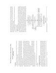
Fig. 2: Example logic block where many pins are not logically equivalent.
a)
b)
c)
Fig. 3: Switch box types
Fc_type {absolute | fractional}: Indicates whether the three Fc values (see
below) should be interpreted as the number of tracks to which each pin connects
(absolute), or the fraction of tracks in a channel to which each pin connects
(fractional).
Fc_input <float>: Sets the number of tracks to which each logic block input pin
connects in each channel bordering the pin. The Fc value used is always the
minimum of the specified Fc and the channel width, W, so you can set Fc to be
huge if you want Fc to always be W.
Fc_output <float>: Sets the number of tracks to which each logic block output pin
connects in each channel bordering the pin.
Fc_pad <float>: Sets the number of tracks to which each I/O pad connects in the
channel bordering the pad.
segment frequency: <float> length: <int | longline> wire_switch: <int>
opin_switch: <int>
Frac_cb: <float> Frac_sb: <float> Rmetal: <float> Cmetal: <float>
Describes a type of segment. You can specify as many types of segments as you
like -- just use one segment line for each. The meaning of each value is:
• frequency: The fraction (from 0 to 1) of routing tracks composed of this type
of segment. The sum of the frequency values for all the segment lines must
be 1 -- i. e. 100% of the tracks have been described.
• length: Either the number of logic blocks spanned by each segment, or the
keyword longline. Longline means segments of this type span the entire
FPGA array.
• wire_switch: The index of the switch type used by other wiring segments to
drive this type of segment. That is, switches going to this segment from other
pieces of wiring will use this type of switch.
• opin_switch: The index of the switch type used by CLB and pad output pins
to drive this type of segment.
• Frac_cb: Describes the internal population of the segment for connection
boxes (connections to logic blocks). This number gives the fraction (from 0 to
1) of logic blocks passed by this segment to which it will have a connection
box. A switch exists from a segment to a logic block pin only if (1) the
segment wants a connection box to that logic block and (2) the logic block
connection box pattern for that pin wants a connection to that segment.
• Frac_sb: Describes the internal population of the segment for switch boxes
(connections to other routing tracks). This number gives the fraction (from 0
to 1) of the length + 1 switch blocks which could exist along the segment that
do in fact exist. So, a segment of length 9 that had a Frac_sb value of 0.5
would have 5 switch boxes along its length. Exactly which tracks a segment
connects to at each switch box is determined by the switch_box_type
parameter.
• Rmetal: Resistance per unit length (in terms of logic blocks) of this wiring
track, in Ohms. For example, a segment of length 5 with Rmetal = 10 Ohms /
logic block would have an end-to-end resistance of 50 Ohms.
• Cmetal: Capacitance per unit length (in terms of logic blocks) of this wiring
track, in Farads. For example, a segment of length 5 with Cmetal = 2e-14 F /
logic block would have a total metal capacitance of 10e-13F. For example,
let’s say an architecture file describes two types of segments.
segment frequency: 0.5 length: 2 wire_switch: 0 opin_switch: 0 Frac_cb: 1. \
Frac_sb: 0.666 Rmetal: 5 Cmetal: 5e-15
segment frequency: 0.5 length: 4 wire_switch: 0 opin_switch: 0 Frac_cb: 0.5 \
Frac_sb: 1. Rmetal: 3 Cmetal: 2e-15
If the FPGA you wish to route has a channel width of 4, one channel will look as
shown in Fig. 4. Notice that 2 tracks (50% of the tracks) are segments of length 2,
and 2 tracks are segments of length four.
Also notice that the number of switch boxes and connection boxes along each
segment has been set in accordance with the Frac_sb and Frac_cb values for
each segment type.
switch <int> buffered: { yes | no } R: <float> Cin: <float> Cout: <float>
Tdel: <float>
Describes a a type of switch. This statement defines what a certain type of
switch is -- segment statements refer to a switch types by their number (the
number right after the switch keyword). The various values are:
• buffered: yes, if this switch is a tri-state buffer, no if this switch is a pass
transistor.
• R: resistance of the switch.
• Cin: Input capacitance of the switch.
• Cout: Output capacitance of the switch.
• Tdel: Intrinsic delay through the switch. If this switch was driven by a zero
resistance source, and
drove a zero capacitance load, its delay would be Tdel + R ∗ C out .
R_minW_nmos <float>: The resistance of minimum-width nmos transistor.
This data is used only
by the area model built into VPR.
R_minW_pmos <float>: The resistance of minimum-width pmos transistor.
This data is used only
by the area model built into VPR.
The lines below give an example of a detailed routing description from a .arch
file.
Fig. 4: Example of a segmented routing channel with four tracks per channel.
switch_block_type planar #Uses the fewest switches on a segmented architecture.
Fc_type fractional #Fc values below are in terms of fraction of W.
Fc_output 1. #clb output pins connect to all W tracks in adjacent channels
# (if each of those tracks wants a connection box there).
Fc_input 0.5 #clb input pins connect to half (0.5 * W) of adjacent tracks
# (if each of those tracks wants a connection box there).
Fc_pad 0.7 # I/O pads connect to 70% (0.7 * W) of adjacent tracks
# (if each of those tracks wants a connection box there).
# 50% of segments are length 2, 50% are length 4. Length two segments are
driven by
# type 1 switches when the connection is coming from another wire, and are driven
# by type 0 switches when the connection comes from a clb output pin.
# The length four segments are always driven by type 0 switches.
segment frequency: 0.5 length: 2 wire_switch: 1 opin_switch: 0 Frac_cb: 1. \
Frac_sb: 0.666 Rmetal: 5 Cmetal: 5e-15
segment frequency: 0.5 length: 4 Frac_cb: 0.5 Frac_sb: 1. Rmetal: 3 \
Cmetal: 2e-15
# In this case, type 1 switches are pass transistors, while type 0 switches are
# tri-state buffers.
switch 1 buffered: no R: 100 Cin: 2e-15 Cout: 2e-15 Tdel: 0 # Pass transistor
switch 0 buffered: yes R: 50 Cin: .5e-15 Cout: 4e-15 Tdel: 1e-11 # Tri-state buffer
R_minW_nmos 100 #Used by area model. Min-width transistor resistances.
R_minW_pmos 200
1.4.
Timing Analysis Parameters
The following parameters are required if timing analysis is to be performed on
the placed and routed circuit, or the timing-driven router is to be used.
C_ipin_cblock <float>: Input capacitance of the buffer isolating a routing track
from the connection boxes (multiplexers) that select the signal to be connected to
a logic block input pin (Fig. 5). One of these buffers is inserted in the FPGA for
each track at each location at which it connects to a connection box. For example,
a routing segment that spans three logic blocks, and connects to logic blocks at
two of these three possible locations would have two isolation buffers attached to
it. If a routing track connects to the logic blocks both above and below it at some
point, only one isolation buffer is inserted at that point. If your connection from
routing track to connection block does not include a buffer, set this parameter to
the capacitive loading a track would see at each point where it connects to a logic
block or blocks.
T_ipin_cblock <float>: Delay to go from a routing track, through the isolation
buffer (if your architecture contains these) and a connection block (typically a
multiplexer) to a logic block input pin.
T_ipad <float>: Delay through an input pad.
T_opad <float>: Delay through an output pad.
T_clb_ipin_to_sblk_ipin <float>: Delay from an input pin of a CLB (logic block) to
an input pin of a subblock within that CLB. For architectures without local routing
(i.e. CLB input pins connect directly to some logic element, like a LUT or
multiplexer) this delay is essentially zero.
T_sblk_opin_to_sblk_ipin <float>: Delay from the output of a subblock to the
input of another subblock within the same CLB. For architectures without local
routing (e.g. the output of one subblock is hardwired to the input of another) this
delay is essentially zero.
T_sblk_opin_to_clb_opin <float>: Delay from the output of a subblock to a
CLB(logic block) output pin. For architectures without local routing (e.g. the output
of a LUT is hardwired to each logic block output), this delay is essentially zero.
T_subblock T_comb: <float> T_seq_in: <float> T_seq_out: <float>
Describes the delays within a subblock. There must be one T_subblock line for
each subblock a logic block can contain -- i.e. there must be subblocks_per_clb of
these T_subblock lines. The first line specifies the delays of subblock zero, which
is the first subblock listed in each CLB in the circuit netlist file. The second
T_subblock line specifies the delay of subblock one, (the second subblock in each
CLB in the circuit netlist file), and so on. If the subblocks within a CLB have
different delays then, you must list them in the same order in the architecture and
netlist files.
The above delays are illustrated in Fig. 6.
Fig. 5: Routing track to logic block connection structure.
Fig. 6: Local routing delays within a logic block (CLB).
• T_comb: The delay from any subblock input to the subblock output when this
subblock is used in combinational mode. A subblock is used in combinational
mode when the netlist leaves its clock pin OPEN.
• T_seq_in: The delay from any subblock input pin to the FF storage element
when this subblock is used in sequential mode. A subblock is used in sequential
mode when the netlist hooks its clock pin to some signal. If this subblock was a
simple flip flop, for example, then T_seq_in is the setup time. If this subblock
corresponds to, say, a LUT feeding into a flip flop, then T_seq_in should be set to
the LUT delay plus the setup time.
• T_seq_out: The delay from the subblock storage element (FF) to the subblock
output pin when this block is used in sequential mode. A subblock is used in
sequential mode when the netlist hooks its clock pin to some signal. If this
subblock had a flip flop hooked to its output pin, for example, then T_seq_out
would be the clock-to-Q delay of the flip flop.
2.
Running DUTYS
As with all tools in the AMDREL tool flow, DUTYS can be executed both from
the command line and using the GUI.
2.1.
Running DUTYS from the command line
DUTYS can be run from the command line by typing dutys at the command
line. The tool then proceeds by asking the user to supply the name of the desired
architecture file. After the name of the new architecture file is typed, the tool
proceeds by asking the user to input the parameters mentioned in the previous
section one by one.
2.2.
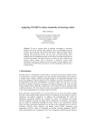
DUTYS GUI
The DUTYS GUI (part from the MEANDER design framework) can be seen in
the Fig. 7. The GUI has a number of fields that need to be filled and each one
corresponds to the questions asked in the command line execution. Next to each
field a short description of the corresponding architecture file parameter is
included. The GUI is available from the URL http://vlsi.ee.duth.gr/amdrel.
Fig. 7: DUTYS GUI