1
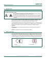
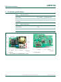
UM10724 TEA1720ADB1152 10 W EVD15 demo board Rev. 1.1 — 6 August 2014 User manual Document information Info Content Keywords TEA1720ADB1152, TEA1720B3T, TEA1705, ultra-low standby power, constant output voltage, constant output current, primary sensing, integrated high-voltage start-up, smartphone and tablet charger, 5 V/2.0 A supply, SMPS transient controller Abstract This user manual describes the TEA1720ADB1152 10 W Constant Voltage/Constant Current (CV/CC) universal input power supply for tablet adapters/chargers. This demo board is based on the GreenChip Smart Power TEA1720B3T and the TEA1705 transient controller. The TEA1720B3T and TEA1705 application enables a no-load power consumption of less than 20 mW and a low external component count for cost-effective applications. In addition, the TEA1720B3T provides advanced control modes for optimal performance. The TEA1705 transient controller continuously monitors the output voltage. When the output voltage drops below the detection level Vdet (VCC), a transient interrupt signal is generated to wake up the TEA1720B3T. UM10724 NXP Semiconductors TEA1720ADB1152 10 W EVD15 demo board Revision history Rev Date Description v.1.1 20140806 updated issue • Modifications: v.1 20131205 The text has been updated throughout the user manual. first issue Contact information For more information, please visit: http://www.nxp.com For sales office addresses, please send an email to: [email protected] UM10724 User manual All information provided in this document is subject to legal disclaimers. Rev. 1.1 — 6 August 2014 © NXP B.V. 2014. All rights reserved. 2 of 31 UM10724 NXP Semiconductors TEA1720ADB1152 10 W EVD15 demo board 1. Introduction WARNING Lethal voltage and fire ignition hazard The non-insulated high voltages that are present when operating this product, constitute a risk of electric shock, personal injury, death and/or ignition of fire. This product is intended for evaluation purposes only. It shall be operated in a designated test area by personnel qualified according to local requirements and labor laws to work with non-insulated mains voltages and high-voltage circuits. This product shall never be operated unattended. This user manual describes the TEA1720ADB1152 10 W Constant Voltage or Constant Current (CV/CC) universal input power supply for tablet adapters and chargers. This demo board is based on the TEA1720B3T GreenChip SP-integrated circuit. The TEA1720B3T GreenChip SP provides ultra-low no-load power consumption without using additional external components. Designs are cost-effective using the TEA1720B3T GreenChip SP because only a few external components are needed in a typical application. The additional TEA1705 transient controller ensures excellent transient response in no-load mode. Remark: All voltages are in V (AC) unless otherwise stated 2. Safety warning The complete demo board application is AC mains voltage powered. Avoid touching the board when power is applied. An isolated housing is obligatory when used in uncontrolled, non-laboratory environments. Always provide galvanic isolation of the mains phase using a variable transformer. The following symbols identify isolated and non-isolated devices. 019aab174 019aab173 a. Isolated Fig 1. UM10724 User manual b. Not Isolated Isolation symbols All information provided in this document is subject to legal disclaimers. Rev. 1.1 — 6 August 2014 © NXP B.V. 2014. All rights reserved. 3 of 31 UM10724 NXP Semiconductors TEA1720ADB1152 10 W EVD15 demo board 3. Features 3.1 Power features • • • • • Low component count for cost-effective design • • • • • Built-in emitter switch for driving low-cost NPN high-voltage transistor Universal mains input Isolated output Highly efficient > 80 % Primary sensing for control of the output voltage without optocoupler and secondary feedback circuitry Minimizes audible noise in all operation modes Energy Star 2.0 compliant Jitter function for reduced EMI Excellent transient performance with ultra low no-load power and small output capacitors • Cable compensation 0.3 V at maximum power 3.2 Green features • No-load power consumption < 20 mW • Very low supply current in no-load condition with energy save mode • Incorporates a high-voltage start-up circuit with zero current consumption under normal switching operation 3.3 Protection features • • • • • • • • UM10724 User manual OverVoltage Protection (OVP) with auto-restart UnderVoltage LockOut (UVLO) and OverVoltage Protection (OVP) on IC supply pin OverTemperature Protection (OTP) Sense pin short protection Hiccup function for automatic switch-off at continuous too low output voltage Demagnetization protection for guaranteed discontinuous conduction mode operation Open and short-circuit protection of the Feedback control (FB) pin Short-circuit protection of the charger output All information provided in this document is subject to legal disclaimers. Rev. 1.1 — 6 August 2014 © NXP B.V. 2014. All rights reserved. 4 of 31 UM10724 NXP Semiconductors TEA1720ADB1152 10 W EVD15 demo board 4. Technical specifications Table 1. Input specifications Parameter Conditions Value Remark input voltage - 90 V to 265 V universal AC mains input frequency - 47 Hz to 63 Hz - average no-load input power consumption no-load 18 mW Table 2. Output specifications Parameter Conditions Value Remark output voltage - 5.0 V - nominal output current - 2.0 A - nominal output power - 10.0 W - a. Top view Fig 2. average of 115 V and 230 V b. Bottom view TEA1720ADB1152 10 W EVD15 demo board UM10724 User manual All information provided in this document is subject to legal disclaimers. Rev. 1.1 — 6 August 2014 © NXP B.V. 2014. All rights reserved. 5 of 31 UM10724 NXP Semiconductors TEA1720ADB1152 10 W EVD15 demo board 5. Performance data 5.1 No-load input power consumption The no-load input power has been measured 20 minutes after switch-on. Table 3 and Figure 3 show the results. Table 3. No-load input power consumption Vmains (V) Output voltage (V) Power consumption (mW) 90 5.213 18.8 115 5.204 18.1 230 5.178 17.5 265 5.168 18.8 DDD 1RORDG SRZHU P: 9PDLQV$& Fig 3. UM10724 User manual No-load input power consumption All information provided in this document is subject to legal disclaimers. Rev. 1.1 — 6 August 2014 © NXP B.V. 2014. All rights reserved. 6 of 31 UM10724 NXP Semiconductors TEA1720ADB1152 10 W EVD15 demo board 5.2 VI curves Figure 4 shows the VI characteristics measured at the PCB end. DDD 9RXW 9 9RXW 9 ,RXW$ a. 90 V (AC) ,RXW$ b. 115 V (AC) DDD DDD 9RXW 9 9RXW 9 c. 230 V (AC) Fig 4. DDD ,RXW$ ,RXW$ d. 265 V (AC) VI characteristics (PCB end) Below Vout = 2.7 V at the PCB end, the controller enters the hiccup mode. UM10724 User manual All information provided in this document is subject to legal disclaimers. Rev. 1.1 — 6 August 2014 © NXP B.V. 2014. All rights reserved. 7 of 31 UM10724 NXP Semiconductors TEA1720ADB1152 10 W EVD15 demo board Figure 5 shows the VI characteristics measured at the cable end. DDD 9RXW 9 9RXW 9 ,RXW$ a. 90 V (AC) ,RXW$ b. 115 V (AC) DDD 9RXW 9 DDD 9RXW 9 c. 230 V (AC) Fig 5. DDD ,RXW$ ,RXW$ d. 265 V (AC) VI characteristics (cable end) Below Vout = 2.4 V at the cable end the controller enters the hiccup mode. UM10724 User manual All information provided in this document is subject to legal disclaimers. Rev. 1.1 — 6 August 2014 © NXP B.V. 2014. All rights reserved. 8 of 31 UM10724 NXP Semiconductors TEA1720ADB1152 10 W EVD15 demo board 5.3 Efficiency Figure 6 shows the efficiency at 90 V, 115 V, 230 V and 265 V. DDD (IILHQF\DW 3&%HQG ORXW$ (1) Efficiency at 90 V (AC) (2) Efficiency at 115 V (AC) (3) Efficiency at 230 V (AC) (4) Efficiency at 265 V (AC) Fig 6. Table 4. Efficiency PCB end Vin (V (AC)) 90 115 230 265 UM10724 User manual Efficiency as a function of output current Iout (A) Vout (V) Pin (W) efficiency (%) Average 0.5 A to 2.0 A 0.20 5.04 1.39 72.25 77.86 0.50 5.07 3.29 76.80 1.00 5.13 6.54 78.27 1.50 5.22 9.98 78.29 2.00 5.33 13.61 78.08 0.20 5.04 1.36 73.77 0.50 5.06 3.20 78.92 1.00 5.12 6.36 80.22 1.50 5.21 9.70 80.40 2.00 5.31 13.14 80.58 0.20 5.06 1.37 73.43 0.50 5.06 3.16 79.86 1.00 5.11 6.23 81.73 1.50 5.21 9.51 81.98 2.00 5.29 12.86 82.15 0.20 5.06 1.40 72.06 0.50 5.06 3.19 79.15 1.00 5.11 6.25 81.52 1.50 5.21 9.53 81.78 2.00 5.29 12.88 82.01 All information provided in this document is subject to legal disclaimers. Rev. 1.1 — 6 August 2014 80.03 81.43 81.12 © NXP B.V. 2014. All rights reserved. 9 of 31 UM10724 NXP Semiconductors TEA1720ADB1152 10 W EVD15 demo board 5.4 Transient response TEA1720B3T The transient response for the TEA1720B3T (300 mV cable compensation) has been tested with load steps at 90 V and 265 V at the PCB end and at the end of the cable from: • 0 A 0.5 A 0 A • 0 A 1.0 A 0 A • 0 A 2.0 A 0 A Figure 7 to Figure 9 show the load step response, measured at PCB end. Red = Vout Red = Vout Orange = Iout Orange = Iout a. 90 V (AC) Fig 7. b. 265 V (AC) Load step 0 A 0.5 A 0 A at PCB end UM10724 User manual All information provided in this document is subject to legal disclaimers. Rev. 1.1 — 6 August 2014 © NXP B.V. 2014. All rights reserved. 10 of 31 UM10724 NXP Semiconductors TEA1720ADB1152 10 W EVD15 demo board Red = Vout Red = Vout Orange = Iout Orange = Iout a. 90 V (AC) Fig 8. b. 265 V (AC) Load step 0 A 1.0 A 0 A at PCB end Red = Vout Red = Vout Orange = Iout Orange = Iout a. 90 V (AC) Fig 9. b. 265 V (AC) Load step 0 A 2.0 A 0 A at PCB end UM10724 User manual All information provided in this document is subject to legal disclaimers. Rev. 1.1 — 6 August 2014 © NXP B.V. 2014. All rights reserved. 11 of 31 UM10724 NXP Semiconductors TEA1720ADB1152 10 W EVD15 demo board Figure 10 to Figure 12 show the load step response measured at cable end (0.15 ). Red = Vout Red = Vout Orange = Iout Orange = Iout a. 90 V (AC) b. 265 V (AC) Fig 10. Load step 0 A 0.5 A 0 A at cable end (0.15 ) Red = Vout Red = Vout Orange = Iout Orange = Iout a. 90 V (AC) b. 265 V (AC) Fig 11. Load step 0 A 1.0 A 0 A at cable end (0.15 ) UM10724 User manual All information provided in this document is subject to legal disclaimers. Rev. 1.1 — 6 August 2014 © NXP B.V. 2014. All rights reserved. 12 of 31 UM10724 NXP Semiconductors TEA1720ADB1152 10 W EVD15 demo board Red = Vout Red = Vout Orange = Iout Orange = Iout a. 90 V (AC) b. 265 V (AC) Fig 12. Load step 0 A 2.0 A 0 A at cable end (0.15 ) UM10724 User manual All information provided in this document is subject to legal disclaimers. Rev. 1.1 — 6 August 2014 © NXP B.V. 2014. All rights reserved. 13 of 31 UM10724 NXP Semiconductors TEA1720ADB1152 10 W EVD15 demo board 5.5 Turn-on delay and output rise time Figure 13 shows the turn-on the delay of the output of the supply at 90 V and 265 V with no-load and 2 A load. Turn-on delay time = 120 ms Turn-on delay time = 122 ms a. 90 V (AC); no-load b. 265 V (AC); no-load Turn-on delay time = 135 ms Turn-on delay time = 144 ms c. 90 V (AC); 2 A load d. 265 V (AC); 2 A load Fig 13. Turn-on delay times at no-load and 2 A load UM10724 User manual All information provided in this document is subject to legal disclaimers. Rev. 1.1 — 6 August 2014 © NXP B.V. 2014. All rights reserved. 14 of 31 UM10724 NXP Semiconductors TEA1720ADB1152 10 W EVD15 demo board Figure 14 shows the rise time of the output from 10 % to 90 % at 90 V and 265 V with no-load and 2 A load. (1) Rise time: 10 % => 90 % = 1.84 ms (1) Rise time: 10 % => 90 % = 1.88 ms (2) Rise time: 0 % => 100 % = 2.35 ms (2) Rise time: 0 % => 100 % = 2.30 ms a. 90 V (AC); no-load b. 265 V (AC); no-load (1) Rise time: 10 % => 90 % = 16.1 ms (1) Rise time: 10 % => 90 % = 24.7 ms (2) Rise time: 0 % => 100 % = 19.6 ms (2) Rise time: 0 % => 100 % = 29.8 ms c. 90 V (AC); 2 A load d. 265 V (AC); 2 A load Fig 14. Output rise time 10 % 90 % at 2 A load UM10724 User manual All information provided in this document is subject to legal disclaimers. Rev. 1.1 — 6 August 2014 © NXP B.V. 2014. All rights reserved. 15 of 31 UM10724 NXP Semiconductors TEA1720ADB1152 10 W EVD15 demo board 5.6 Output voltage ripple and noise performance The output voltage ripple and noise performance has been measured with an oscilloscope probe connected to the output of the demo board. A probe tip was used with a very short GND connection. A 100 nF ceramic capacitor and a 10 F electrolytic capacitor are used in parallel with the probe tip to terminate the output. The output voltage ripple and noise has been measured at 90 V and 265 V both at no-load and 2 A load. Figure 15 and Figure 16 show the results. a. 90 V (AC) b. 265 V (AC) Fig 15. Output voltage ripple and noise; no-load; cable end (0.15 ) a. 90 V (AC) b. 265 V (AC) Fig 16. Output voltage ripple and noise; 2 A load; cable end (0.15 ) UM10724 User manual All information provided in this document is subject to legal disclaimers. Rev. 1.1 — 6 August 2014 © NXP B.V. 2014. All rights reserved. 16 of 31 UM10724 NXP Semiconductors TEA1720ADB1152 10 W EVD15 demo board 5.7 Inrush current The inrush current is limited in the demo board by an NTC in series with the mains. Table 5 shows the value of the peak inrush current. Table 5. Inrush current (A peak) Vin (V) 90 V 115 V 230 V 265 V Iout = 0 A 8.3 A peak 11.0 A peak 23.3 A peak 27.3 A peak Iout = 2 A 8.6 A peak 11.1 A peak 24.1 A peak 27.6 A peak 5.8 Short circuit When the output is shorted, the controller enters hiccup mode. The input power and average output current is given in Table 6. Table 6. Short circuit input power and average output current 90 V (AC) 265 V (AC) input power Shorted output 0.97 W 0.87 W average output current 0.88 A 0.63 A 5.9 Conducted EMI The conducted EMI is measured according to EN55022 without the secondary GND connected to the protective mains ground and from 150 kHz to 30 MHz. Figure 17 and Figure 18 show the results. The red crosses show the quasi peak values. Fig 17. Conducted EMI 115 V; no ground; 2 A load UM10724 User manual All information provided in this document is subject to legal disclaimers. Rev. 1.1 — 6 August 2014 © NXP B.V. 2014. All rights reserved. 17 of 31 UM10724 NXP Semiconductors TEA1720ADB1152 10 W EVD15 demo board Fig 18. Conducted EMI 230 V; no ground; 2 A load UM10724 User manual All information provided in this document is subject to legal disclaimers. Rev. 1.1 — 6 August 2014 © NXP B.V. 2014. All rights reserved. 18 of 31 UM10724 NXP Semiconductors TEA1720ADB1152 10 W EVD15 demo board 5.10 Radiated EMI The radiated EMI is measured according to EN 55022 (30 MHz to 1 GHz). Figure 19 and Figure 20 show the measured results. Fig 19. Radiated EMI at 115 V/2 A load Fig 20. Radiated EMI at 230 V/2 A load UM10724 User manual All information provided in this document is subject to legal disclaimers. Rev. 1.1 — 6 August 2014 © NXP B.V. 2014. All rights reserved. 19 of 31 UM10724 NXP Semiconductors TEA1720ADB1152 10 W EVD15 demo board 5.11 Common-mode noise Figure 21 shows the result of the EPS switching frequency component of the common-mode noise test. The switching component is below 2 Vpp. Fig 21. Common-mode noise EPS switching frequency component at 265 V 5.11.1 Test description The TEA1720ADB1152 demo board has been connected to a 265 V (AC) power source where one or the other of the AC mains is a neutral conductor. It has been connected to the protected earth ground either at the upstream service transformer, or locally in the laboratory environment. The demo board has been loaded with a 5 , 1 %, resistive load, at the end of a 1 meter USB cable. The 5 load is located in a metal box that represents the equivalent capacitive load of a generic mobile terminal. The EPS switching component has been measured with an 1:100 oscilloscope probe (50 M // 7.5 pF) between the metal box ground and the protective earth ground. The level of the common-mode noise is measured at the worst position, which is around the mains voltage zero crossing in this case. The test has been repeated with a 2.5 resistor load. The test result was equal to the 5 test result. UM10724 User manual All information provided in this document is subject to legal disclaimers. Rev. 1.1 — 6 August 2014 © NXP B.V. 2014. All rights reserved. 20 of 31 UM10724 NXP Semiconductors TEA1720ADB1152 10 W EVD15 demo board 5.12 Thermal measurements The component temperatures were measured using a temperature chamber. The PCB was placed inside an encasing. To avoid influence of the air flow, the encasing itself is placed inside a box (see Figure 22). 7HPSHUDWXUHFKDPEHU ,VRODWLRQER[WRDYRLGDLUIORZ7HPSHUDWXUHFKDPEHU &KDUJHUFDVLQJ 7UDIR 131 &KDPEHUWHPSHUDWXUH&& DDD Fig 22. Measurement setup temperature chamber The component temperatures are measured using thermocouples, glued on the components. The temperatures after 30 minutes warming-up time at 2 A load are shown in Table 7. Table 7. Component temperatures at 2 A load and Tambient = 25 C/45 C Chamber temperature UM10724 User manual Vin = 90 V; Iout = 2 A Vin = 265 V; Iout = 2 A Temperature (C) Temperature (C) 25 45 25 45 1 EVD15 transformer 67 83 66 84 2 TB100 NPN 83 99 90 109 3 TEA1720 controller 73 89 57 65 4 D50/D51 secondary diodes 73 88 72 88 5 R770/71/72 base resistors 90 103 73 92 6 C52 output capacitor 58 75 58 75 7 C2 input capacitor 69 83 60 78 All information provided in this document is subject to legal disclaimers. Rev. 1.1 — 6 August 2014 © NXP B.V. 2014. All rights reserved. 21 of 31 xxxxxxxxxxxxxxxxxxxxx xxxxxxxxxxxxxxxxxxxxxxxxxx xxxxxxx x x x xxxxxxxxxxxxxxxxxxxxxxxxxxxxxx xxxxxxxxxxxxxxxxxxx xx xx xxxxx xxxxxxxxxxxxxxxxxxxxxxxxxxx xxxxxxxxxxxxxxxxxxx xxxxxx xxxxxxxxxxxxxxxxxxxxxxxxxxxxxxxxxxx xxxxxxxxxxxx x x xxxxxxxxxxxxxxxxxxxxx xxxxxxxxxxxxxxxxxxxxxxxxxxxxxx xxxxx xxxxxxxxxxxxxxxxxxxxxxxxxxxxxxxxxxxxxxxxxxxxxxxxxx xxxxxxxx xxxxxxxxxxxxxxxxxxxxxxxxx xxxxxxxxxxxxxxxxxxxx xxx NXP Semiconductors UM10724 User manual 6. Schematic 7 WUDQVIRUPHU(9' / + )/ 3 - / )/ 0 ' & Q) 9 6%5863 5) $7 ' 6-/ 5 Nȍ 7 57 ȍ 5 ȍ 5 ȍ & S) 9 ' %$6 ' ȍ &$3 ' 60/ & S) N9 (6$/ 5 4 7% & Q) 9 ' 60/ & ) 9 ' 60/ ' 60/ QF )% *1'7(67 - 1 7($%7 *1' Q) 9 9&& ' & ) 9 6 6 9 ' 5 Nȍ *1' 6 6 *1' 5 Nȍ ȍ 8 627 & ) 9 5 5 +9 7($ ȍ ȍ & ) 9 8 ' %=;& 6%5863 & 5 5 ȍ & ) 9 5 Nȍ (0,77(5 9&& 6(16( *1' 5 ȍ & S) 9 5 Nȍ / 5 ȍ 5 ȍ & ) 9 + DDD UM10724 22 of 31 © NXP B.V. 2014. All rights reserved. Fig 23. Schematic TEA1720ADB1152 10 W EVD15 demo board TEA1720ADB1152 10 W EVD15 demo board Rev. 1.1 — 6 August 2014 All information provided in this document is subject to legal disclaimers. 5 Nȍ - 86%$IODW ' UM10724 NXP Semiconductors TEA1720ADB1152 10 W EVD15 demo board 7. Circuit description The GreenChip TEA1720ADB1152 demo board consists of a single-phase full wave rectifier circuit, a filtering section, a switching section, an output section and a feedback section. The circuit diagram is shown in Figure 23 and the component list is shown in Table 8. 7.1 Rectification section The bridge diodes D101 to D104 provide a single-phase full wave rectifier. Capacitors C1 and C2 function as reservoir capacitors for the rectified input voltage. Thermistor RT1 limits inrush current. Terminals J1 and J2 connect the input to the electricity utility network. Swapping these two wires has no effect on the operation of the converter. 7.2 Filtering section Inductors L1 and L2, with capacitors C1 and C2, form -filters to attenuate conducted differential-mode EMI noise. 7.3 TEA1720B3T section The TEA1720B3T device (U1) contains the oscillator, CV/CC control, start-up control, protection functions, high-voltage start-up and emitter switch for switching the external NPN all in one IC. One auxiliary winding on transformer T1 is used to provide the primary sensing information for the TEA1720B3T. A second auxiliary winding generates the supply voltage. This voltage is (half wave) rectified by diode D5 and capacitor C70. C70 is charged via the current limiter resistor R5. The voltage on C70 is the supply voltage for the VCC pin of the TEA1720B3T and delivers the base current for the NPN transistor. The RCD-R clamp consisting of R8, C8, D8 and R9 limits drain voltage spikes caused by leakage inductance of the transformer. 7.4 Output section Diodes D50 and D51, Schottky barrier type diodes, filtered by capacitors C51 and C52 rectify the secondary winding of transformer T1. Using a Schottky barrier type diode results in a higher efficiency of the demo board. C51 and C52 must have sufficient low ESR characteristics to meet the output voltage ripple and noise requirement without adding an LC output filter. Capacitor C11 damps high frequency ringing and reduces the voltage stress on the Schottky diodes. Resistor R50 provides a minimum load to maintain output control in no-load condition. 7.5 Feedback section The TEA1720B3T controls the output by current and frequency control for CV / CC regulation. The auxiliary winding on Transformer T1 senses the output voltage. The FB pin of the TEA1720B3T senses the reflected output voltage via feedback resistors R30, R31 and R3. C3 is added for noise filtering. UM10724 User manual All information provided in this document is subject to legal disclaimers. Rev. 1.1 — 6 August 2014 © NXP B.V. 2014. All rights reserved. 23 of 31 UM10724 NXP Semiconductors TEA1720ADB1152 10 W EVD15 demo board 7.6 Transient controller The TEA1705 secondary side transient controller offers an excellent transient response of the TEA1720B3T controller, with ultra-low no-load power and minimum sized output capacitors. The output voltage is continuously monitored and when the output voltage is below the detection level Vdet (VCC), a transient interrupt signal is generated. This signal is transmitted via C10 and the transformer to the primary side to wake up the TEA1720B3T. This system reduces the volume of the output capacitors and makes it possible to build compact chargers. 8. PCB layout a. Top b. Bottom Fig 24. Silk screen layers a. Top b. Bottom Fig 25. Copper layers UM10724 User manual All information provided in this document is subject to legal disclaimers. Rev. 1.1 — 6 August 2014 © NXP B.V. 2014. All rights reserved. 24 of 31 UM10724 NXP Semiconductors TEA1720ADB1152 10 W EVD15 demo board 9. Bill Of Material (BOM) Table 8. TEA1720ADB1152 bill of material Reference Description and values Part number Manufacturer C1 capacitor; 10 F; 400 V; 8 14 mm ERK2GM100F12OT Aishi C2 capacitor: 10 F; 400 V; 8 14 mm ERK2GM100F12OT Aishi C3 capacitor; 33 pF; 50 V; X7R; C0603 - - C7 capacitor; 3.3 nF; 50 V; X7R; C0805 - - C8 capacitor; 220 pF; 500 V; C0805 CC0805JRNPOBBN221 Yageo C10 capacitor; 47 nF; 50 V; X7R; C0603 - - C11 capacitor; 2.2 nF; 50 V; X7R; C0603 - - C51 capacitor; 470 F; 6.3 V; 5 8 mm RS80J471MDNASQJT Nichicon C52 capacitor; 470 F; 6.3 V; 5 8 mm RS80J471MDNASQJT Nichicon C53 capacitor; 22 F; 10 V; 1206 GRM31CR71A226KE15L Murata C70 capacitor; 10 F; 35 V; C1206 C3216X7R1V106M160AC TDK C100 capacitor; 100 pF; 2000 V CD70-B2GA101KYNS TDK D1 diode; 30 V; BZX384-C43 BZX384-C43 NXP Semiconductors D5 diode; 100 V; BAS316; SOD323 BAS316 NXP Semiconductors D7 diode; 50 V; ES1AL; SMF ES1AL Taiwan Semiconductor D8 diode; 600 V; S1JL S1J Taiwan Semiconductor D50 diode; 45 V; SBR10U45SP5-13 SBR10U45SP5-13 Diodes Inc. D51 diode; 45 V; SBR10U45SP5-13 SBR10U45SP5-13 Diodes Inc. D101 diode; 1000 V; S1ML S1ML Taiwan Semiconductor D102 diode; 1000 V; S1ML S1ML Taiwan Semiconductor D103 diode; 1000 V; S1ML S1ML Taiwan Semiconductor D104 diode; 1000 V; S1ML S1ML Taiwan Semiconductor J3 connector USB AF DIP -094-H Gold Conn L101 inductor; 100 H; 11R104C Murata L102 inductor; 10 H; 0805 LBR2012T100K Taiyo Yuden Q1 NPN transistor; T0-92 TB100 NXP Semiconductors R1 resistor; 4.7 k; 1 %; 0805 - - R3 resistor; 4.3 k; 1 %; 0603 - - R5 resistor; 1 ; 1 %; 0603 - - R8 resistor; 100 k; 1206 - - UM10724 User manual All information provided in this document is subject to legal disclaimers. Rev. 1.1 — 6 August 2014 © NXP B.V. 2014. All rights reserved. 25 of 31 UM10724 NXP Semiconductors TEA1720ADB1152 10 W EVD15 demo board Table 8. TEA1720ADB1152 bill of material …continued Reference Description and values Part number Manufacturer R9 resistor; 180 ; 1206 - - R10 resistor; 4.7 ; 0603 - - R11 resistor; 0 ; 0603 - - R30 resistor; 13 k; 1 %; 0603 - - R31 resistor; 200 k; 1 %; 0603 - - R50 resistor; 2.4 k; 0603 - - R60 resistor; 0.75 ; 0805 ERJ6BQFR75V Panasonic R61 resistor; 6.8 ; 1 %; 0805 - - R70 resistor; 430 ; 1 %; 1206 - - R71 resistor; 430 ; 1 %; 1206 - - R72 resistor; 430 ; 1206 - - R102 resistor; 510 ; 0603 - - RT1 thermistor; NTC NTCLE100E3109JB0 Vishay RF1 Fusistor; 2 A; 250 V (AC); 3.18 7.6 mm MCPMP 2 A 250 V Multicomp T1 transformer; EVD15 - - U1 IC; TEA1720B3T; 700 V; SO8 TEA1720B3T NXP Semiconductors U2 IC; TEA1705; SOT23 NXP Semiconductors UM10724 User manual TEA1705 All information provided in this document is subject to legal disclaimers. Rev. 1.1 — 6 August 2014 © NXP B.V. 2014. All rights reserved. 26 of 31 UM10724 NXP Semiconductors TEA1720ADB1152 10 W EVD15 demo board 10. Transformer design 10.1 Transformer schematic design and winding construction The transformer used in the TEA1720ADB1152 demo board has size EVD15 with bobbin EVD15/17/6 horizontal, 8-pin. %RWWRPYLHZ(9' 3ULP WXUQVP 3ULP WXUQVP $X[ *1' 3ULP )O\LQJOHDGV )E WXUQV[P $X[ WXUQVP 6KLHOG *1' 6HF WXUQV [P [P 6HF )E )O\LQJOHDGV 6KLHOG WXUQ 3ULP QF )O\LQJOHDGV )O\LQJOHDGV DDD DDD a. Schematic b. Bottom view Fig 26. EVD15 Transformer schematic and bottom view 10.2 Construction DX[ SULP VKLHOG VHF IE SULP DDD Black dot: Winding direction Fig 27. EVD15 construction Table 9. UM10724 User manual Winding data Layer No. Color Winding Wires parallel No. of turns Wire diameter 11 orange auxiliary winding 1 17 150 m 10 black isolation tape 9 blue primary (sandwich) 1 46 to 48 200 m 8 black isolation tape 7 green shield 6 black isolation tape All information provided in this document is subject to legal disclaimers. Rev. 1.1 — 6 August 2014 1 © NXP B.V. 2014. All rights reserved. 27 of 31 UM10724 NXP Semiconductors TEA1720ADB1152 10 W EVD15 demo board Table 9. Winding data …continued Layer No. Color Winding Wires parallel No. of turns Wire diameter 5 yellow secondary winding 3 6 2 350 m T/W 1 300 m T/W 4 black isolation tape 3 red fb winding 2 black isolation tape 1 blue primary (sandwich) 6 11 130 m 1 46 to 48 200 m Primary-inductance = 930 H 10.3 Specification core and bobbin The specification of the core and bobbin are given on the following pages. Contact Elettronica Rossoni HK Limited for more information. VT 'LPHQVLRQVLQPP DDD Fig 28. Physical data bobbin UM10724 User manual All information provided in this document is subject to legal disclaimers. Rev. 1.1 — 6 August 2014 © NXP B.V. 2014. All rights reserved. 28 of 31 UM10724 NXP Semiconductors TEA1720ADB1152 10 W EVD15 demo board 'LPHQVLRQVLQPP DDD Fig 29. Physical data core Table 10. Core parameters Core parameters effective length (Le) 37.9 mm effective cross area (Ae) 26.1 mm2 effective volume (Ve) 990 mm3 approximate weight (W) 5.7 gram/pair 11. Points of attention When testing the CC-mode of the TEA1720B3T, it is necessary to use a DC electronic load in resistive mode, not in current mode. The current in CC-mode has a small fold back characteristic (see Figure 4 and Figure 5). When current mode of a DC electronic load is used, the output voltage drops immediate to zero when the maximum current is exceeded. When the output voltage becomes zero, causing the input voltage of the used DC electronic load to become zero as well, many DC electronic loads can no longer adjust the current. Using the resistive mode of the DC electronic load avoids this problem. Below Vout = 2.7 V at the PCB end, the TEA1720B3T enters hiccup mode to limit the output power. Remark: This behavior of the TEA1720B3T controller is not incorrect. It is only required to test it in the correct way. UM10724 User manual All information provided in this document is subject to legal disclaimers. Rev. 1.1 — 6 August 2014 © NXP B.V. 2014. All rights reserved. 29 of 31 UM10724 NXP Semiconductors TEA1720ADB1152 10 W EVD15 demo board 12. Legal information 12.1 Definitions Draft — The document is a draft version only. The content is still under internal review and subject to formal approval, which may result in modifications or additions. NXP Semiconductors does not give any representations or warranties as to the accuracy or completeness of information included herein and shall have no liability for the consequences of use of such information. NXP Semiconductors does not accept any liability related to any default, damage, costs or problem which is based on any weakness or default in the customer’s applications or products, or the application or use by customer’s third party customer(s). Customer is responsible for doing all necessary testing for the customer’s applications and products using NXP Semiconductors products in order to avoid a default of the applications and the products or of the application or use by customer’s third party customer(s). NXP does not accept any liability in this respect. Export control — This document as well as the item(s) described herein may be subject to export control regulations. Export might require a prior authorization from competent authorities. 12.2 Disclaimers Limited warranty and liability — Information in this document is believed to be accurate and reliable. However, NXP Semiconductors does not give any representations or warranties, expressed or implied, as to the accuracy or completeness of such information and shall have no liability for the consequences of use of such information. NXP Semiconductors takes no responsibility for the content in this document if provided by an information source outside of NXP Semiconductors. In no event shall NXP Semiconductors be liable for any indirect, incidental, punitive, special or consequential damages (including - without limitation - lost profits, lost savings, business interruption, costs related to the removal or replacement of any products or rework charges) whether or not such damages are based on tort (including negligence), warranty, breach of contract or any other legal theory. Notwithstanding any damages that customer might incur for any reason whatsoever, NXP Semiconductors’ aggregate and cumulative liability towards customer for the products described herein shall be limited in accordance with the Terms and conditions of commercial sale of NXP Semiconductors. Right to make changes — NXP Semiconductors reserves the right to make changes to information published in this document, including without limitation specifications and product descriptions, at any time and without notice. This document supersedes and replaces all information supplied prior to the publication hereof. Suitability for use — NXP Semiconductors products are not designed, authorized or warranted to be suitable for use in life support, life-critical or safety-critical systems or equipment, nor in applications where failure or malfunction of an NXP Semiconductors product can reasonably be expected to result in personal injury, death or severe property or environmental damage. NXP Semiconductors and its suppliers accept no liability for inclusion and/or use of NXP Semiconductors products in such equipment or applications and therefore such inclusion and/or use is at the customer’s own risk. Applications — Applications that are described herein for any of these products are for illustrative purposes only. NXP Semiconductors makes no representation or warranty that such applications will be suitable for the specified use without further testing or modification. Customers are responsible for the design and operation of their applications and products using NXP Semiconductors products, and NXP Semiconductors accepts no liability for any assistance with applications or customer product design. It is customer’s sole responsibility to determine whether the NXP Semiconductors product is suitable and fit for the customer’s applications and products planned, as well as for the planned application and use of customer’s third party customer(s). Customers should provide appropriate design and operating safeguards to minimize the risks associated with their applications and products. Evaluation products — This product is provided on an “as is” and “with all faults” basis for evaluation purposes only. NXP Semiconductors, its affiliates and their suppliers expressly disclaim all warranties, whether express, implied or statutory, including but not limited to the implied warranties of non-infringement, merchantability and fitness for a particular purpose. The entire risk as to the quality, or arising out of the use or performance, of this product remains with customer. In no event shall NXP Semiconductors, its affiliates or their suppliers be liable to customer for any special, indirect, consequential, punitive or incidental damages (including without limitation damages for loss of business, business interruption, loss of use, loss of data or information, and the like) arising out the use of or inability to use the product, whether or not based on tort (including negligence), strict liability, breach of contract, breach of warranty or any other theory, even if advised of the possibility of such damages. Notwithstanding any damages that customer might incur for any reason whatsoever (including without limitation, all damages referenced above and all direct or general damages), the entire liability of NXP Semiconductors, its affiliates and their suppliers and customer’s exclusive remedy for all of the foregoing shall be limited to actual damages incurred by customer based on reasonable reliance up to the greater of the amount actually paid by customer for the product or five dollars (US$5.00). The foregoing limitations, exclusions and disclaimers shall apply to the maximum extent permitted by applicable law, even if any remedy fails of its essential purpose. Safety of high-voltage evaluation products — The non-insulated high voltages that are present when operating this product, constitute a risk of electric shock, personal injury, death and/or ignition of fire. This product is intended for evaluation purposes only. It shall be operated in a designated test area by personnel that is qualified according to local requirements and labor laws to work with non-insulated mains voltages and high-voltage circuits. The product does not comply with IEC 60950 based national or regional safety standards. NXP Semiconductors does not accept any liability for damages incurred due to inappropriate use of this product or related to non-insulated high voltages. Any use of this product is at customer’s own risk and liability. The customer shall fully indemnify and hold harmless NXP Semiconductors from any liability, damages and claims resulting from the use of the product. Translations — A non-English (translated) version of a document is for reference only. The English version shall prevail in case of any discrepancy between the translated and English versions. 12.3 Trademarks Notice: All referenced brands, product names, service names and trademarks are the property of their respective owners. GreenChip — is a trademark of NXP Semiconductors N.V. UM10724 User manual All information provided in this document is subject to legal disclaimers. Rev. 1.1 — 6 August 2014 © NXP B.V. 2014. All rights reserved. 30 of 31 UM10724 NXP Semiconductors TEA1720ADB1152 10 W EVD15 demo board 13. Contents 1 2 3 3.1 3.2 3.3 4 5 5.1 5.2 5.3 5.4 5.5 5.6 5.7 5.8 5.9 5.10 5.11 5.11.1 5.12 6 7 7.1 7.2 7.3 7.4 7.5 7.6 8 9 10 10.1 10.2 10.3 11 12 12.1 12.2 12.3 13 Introduction . . . . . . . . . . . . . . . . . . . . . . . . . . . . 3 Safety warning . . . . . . . . . . . . . . . . . . . . . . . . . . 3 Features . . . . . . . . . . . . . . . . . . . . . . . . . . . . . . . 4 Power features . . . . . . . . . . . . . . . . . . . . . . . . . 4 Green features . . . . . . . . . . . . . . . . . . . . . . . . . 4 Protection features . . . . . . . . . . . . . . . . . . . . . . 4 Technical specifications . . . . . . . . . . . . . . . . . . 5 Performance data. . . . . . . . . . . . . . . . . . . . . . . . 6 No-load input power consumption . . . . . . . . . . 6 VI curves. . . . . . . . . . . . . . . . . . . . . . . . . . . . . . 7 Efficiency . . . . . . . . . . . . . . . . . . . . . . . . . . . . . 9 Transient response TEA1720B3T . . . . . . . . . 10 Turn-on delay and output rise time . . . . . . . . . 14 Output voltage ripple and noise performance. 16 Inrush current . . . . . . . . . . . . . . . . . . . . . . . . . 17 Short circuit. . . . . . . . . . . . . . . . . . . . . . . . . . . 17 Conducted EMI . . . . . . . . . . . . . . . . . . . . . . . . 17 Radiated EMI . . . . . . . . . . . . . . . . . . . . . . . . . 19 Common-mode noise . . . . . . . . . . . . . . . . . . . 20 Test description. . . . . . . . . . . . . . . . . . . . . . . . 20 Thermal measurements . . . . . . . . . . . . . . . . . 21 Schematic . . . . . . . . . . . . . . . . . . . . . . . . . . . . . 22 Circuit description . . . . . . . . . . . . . . . . . . . . . . 23 Rectification section . . . . . . . . . . . . . . . . . . . . 23 Filtering section . . . . . . . . . . . . . . . . . . . . . . . 23 TEA1720B3T section . . . . . . . . . . . . . . . . . . . 23 Output section . . . . . . . . . . . . . . . . . . . . . . . . 23 Feedback section . . . . . . . . . . . . . . . . . . . . . . 23 Transient controller . . . . . . . . . . . . . . . . . . . . . 24 PCB layout . . . . . . . . . . . . . . . . . . . . . . . . . . . . 24 Bill Of Material (BOM) . . . . . . . . . . . . . . . . . . . 25 Transformer design . . . . . . . . . . . . . . . . . . . . . 27 Transformer schematic design and winding construction . . . . . . . . . . . . . . . . . . . . . . . . . . 27 Construction . . . . . . . . . . . . . . . . . . . . . . . . . . 27 Specification core and bobbin. . . . . . . . . . . . . 28 Points of attention . . . . . . . . . . . . . . . . . . . . . . 29 Legal information. . . . . . . . . . . . . . . . . . . . . . . 30 Definitions . . . . . . . . . . . . . . . . . . . . . . . . . . . . 30 Disclaimers . . . . . . . . . . . . . . . . . . . . . . . . . . . 30 Trademarks. . . . . . . . . . . . . . . . . . . . . . . . . . . 30 Contents . . . . . . . . . . . . . . . . . . . . . . . . . . . . . . 31 Please be aware that important notices concerning this document and the product(s) described herein, have been included in section ‘Legal information’. © NXP B.V. 2014. All rights reserved. For more information, please visit: http://www.nxp.com For sales office addresses, please send an email to: [email protected] Date of release: 6 August 2014 Document identifier: UM10724