1
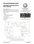
CONTENTS
CHAPTER 1
INTRODUCTION OF THE AHA-HSMC............................................................................................ 1
1.1 Features ......................................................................................................................................................1
1.2 About the KIT.............................................................................................................................................2
1.3 Getting Help ...............................................................................................................................................3
CHAPTER 2
AHA CARD ARCHITECTURE............................................................................................................ 4
2.1 Layout and Components.............................................................................................................................4
2.2 Block Diagram of the ISB Board ...............................................................................................................6
CHAPTER 3
BOARD COMPONENTS ..................................................................................................................... 8
3.1 HSMC Expansion Connector .....................................................................................................................8
3.2 Aptina Parallel Port Interface ................................................................................................................... 11
CHAPTER 4
DEMONSTRATIONS ......................................................................................................................... 13
4.1 Design Concept ........................................................................................................................................13
4.2 Demonstration for Altera DE2-115 FPGA Board.....................................................................................14
4.3 Demonstration for Cyclone III Development Board ................................................................................16
CHAPTER 5
APPENDIX ......................................................................................................................................... 19
5.1 Revision History.......................................................................................................................................19
5.2 Copyright Statement .................................................................................................................................19
I
Chapter 1
Introduction of the AHA-HSMC
FPGAs and image processing are two terms that are becoming linked together in recent years. This
is due to the strong advantages FPGAs present when entering into the realm of video and images.
By utilizing the inherent parallel structures and computation possible in an FPGA, algorithmic
speed is increased dramatically. The birth of the AHA-HSMC daughter card combines the abilities
of two giants in the FPGA industry and the image processing industry: Altera Corporation and
Aptina Imaging Corporation.
The AHA-HSMC is Terasic Technologies’ daughter card solution for sensors from Aptina Imaging
Corporation. The AHA-HSMC makes it possible for users with High Speed Mezzanine Connector
(HSMC) ports to connect Aptina image sensors to Altera FPGA development kits.
1.1 Features
Figure 1-1 shows a photograph of the AHA-HSMC Daughter Card.
1
Figure 1-1 Layout of the AHA-HSMC card
The key features of the card are listed below:
•
•
•
•
Supports I2C configuration for Aptina sensor
Support for standard Aptina parallel interface
Support for Altera HSMC interface
Shutter control function for Aptina Sensor
1.2 About the KIT
The AHA-HSMC kit will come with the following contents:
•
•
AHA-HSMC Daughter Card
System CD-ROM
The system CD contains technical documents of the AHA-HSMC daughter card, which includes
components datasheet, reference designs, demonstrations, schematics, cable and user manual (this
manual).
Figure 1-2 shows the photograph of the AHA-HSMC kit content.
2
Figure 1-2 AHA-HSMC kit package contents
1.3 Getting Help
Here is information of how to get help if you encounter any problem:
•
Terasic Technologies
•
Tel: +886-3-550-8800
•
Email: [email protected]
3
Chapter 2
AHA-HSMC Card Architecture
This chapter provides information about architecture and block diagram of the AHA-HSMC card.
2.1 Layout and Components
The picture of the AHA-HSMC card is shown in Figure 2-1 and Figure 2-2. It depicts the layout of
the board and indicates the locations of the connectors and key components.
4
Figure 2-1 The AHA-HSMC Card PCB and component diagram (top view)
5
Figure 2-2 The AHA-HSMC Card PCB and component diagram (bottom view)
2.2 Block Diagram of the AHA Board
Figure 2-3 shows the block diagram of the AHA-HSMC card. The HSMC connector is housing all
the wires from peripheral interfaces and makes direct connection to FPGA on the main board.
6
Figure 2-3 Block Diagram of AHA-HSMC card
7
Chapter 3
Board Components
3.1 HSMC Expansion Connector
The HSMC interface provides a mechanism to extend the peripheral set of an FPGA host board by
means of a mezzanine card, which can address today’s high speed signaling requirement as well as
standard or legacy low-speed device interface support. Table 3-1
lists the pin assignments of the HSMC connector.
Table 3-1 Pin assignments and descriptions on HSMC connector
Pin Numbers
1-41
42
43
44
45
46
47
48
49
50
51
52
53
54
55
56
57
58
59
60
Name
IMG_IN_FV
CK_FPGA_MCLK
VCC3P3
VCC12
IMG_IN_LV
VCC3P3
VCC12
IMG_DIN3
VCC3P3
VCC12
IMG_DIN2
Direction
Input
Output
Power
Power
Input
Power
Power
Input
Power
Power
Input
8
Description
Frame valid
External clock for sensor
Power 3.3V
Power 12V
Line valid
Power 3.3V
Power 12V
Pixel data
Power 3.3V
Power 12V
Pixel data
61
62
63
64
65
66
67
68
69
70
71
72
73
74
75
76
77
78
79
80
81
82
83
84
85
86
87
88
89
90
91
92
93
94
95
96
97
98
99
100
101
102
103
104
105
SENSOR_RST
VCC3P3
VCC12
IMG_DIN11
SHUTTER
VCC3P3
VCC12
IMG_DIN10
DEMO2_I2C_SCL
VCC3P3
VCC12
IMG_DIN9
DEMO2_I2C_SDA
VCC3P3
VCC12
IMG_DIN8
BUF_HISPI_CLK0_EN
VCC3P3
VCC12
IMG_DIN7
BUF_HISPI_DATA0_EN
VCC3P3
VCC12
CK_IMG_IN_PIXCLK
VCC3P3
VCC12
IMG_DIN6
BUF_HISPI_DATA1_EN
VCC3P3
Output
Power
Power
Input
Output
Power
Power
Input
Output
Power
Power
Input
Input/Output
Power
Power
Input
Output
Power
Power
Input
Output
Power
Power
Input
Power
Power
Input
Output
Power
9
sensor reset
Power 3.3V
Power 12V
Pixel data (MSB)
Shutter
Power 3.3V
Power 12V
Pixel data
Serial clock
Power 3.3V
Power 12V
Pixel data
Serial data
Power 3.3V
Power 12V
Pixel data
LVDS outputs enable
Power 3.3V
Power 12V
Pixel data
LVDS outputs enable
Power 3.3V
Power 12V
Pixel clock
Power 3.3V
Power 12V
Pixel data
LVDS outputs enable
Power 3.3V
106
107
108
109
110
111
112
113
114
115
116
117
118
119
120
121
122
123
124
125
126
127
128
129
130
131
132
133
134
135
136
137
138
139
140
141
142
143
144
145
146
147
148
149
150
VCC12
IMG_DIN5
BUF_HISPI_DATA2_EN
VCC3P3
VCC12
IMG_DIN4
BUF_HISPI_DATA3_EN
VCC3P3
VCC12
IMG_DIN1
VCC3P3
VCC12
IMG_DIN0
VCC3P3
VCC12
LVDS_DATA0_P
LVDS_DATA0_N
VCC3P3
VCC12
LVDS_DATA2_P
LVDS_DATA2_N
VCC3P3
VCC12
LVDS_DATA3_P
LVDS_DATA3_N
VCC3P3
VCC12
LVDS_DATA1_P
Power
Input
Output
Power
Power
Input
Output
Power
Power
Input
Power
Power
Input
Power
Power
Input
Input
Power
Power
Input
Input
Power
Power
Input
Input
Power
Power
Input
10
Power 12V
Pixel data
LVDS outputs enable
Power 3.3V
Power 12V
Pixel data
LVDS outputs enable
Power 3.3V
Power 12V
Pixel data
Power 3.3V
Power 12V
Pixel data
Power 3.3V
Power 12V
HISPI serial data differential P
HISPI serial data differential N
Power 3.3V
Power 12V
HISPI serial data differential P
HISPI serial data differential N
Power 3.3V
Power 12V
HISPI serial data differential P
HISPI serial data differential N
Power 3.3V
Power 12V
HISPI serial data differential P
151
152
153
154
155
156
157
158
159
160
LVDS_DATA1_N
VCC3P3
VCC12
CK_LVDS_CLK0_P
CK_LVDS_CLK0_N
VCC3P3
GND
Input
Power
Power
Input
Input
Power
Power
HISPI serial data differential N
Power 3.3V
Power 12V
HISPI serial clock differential P
HISPI serial clock differential N
Power 3.3V
Power Ground
3.2 Aptina Parallel Port Interface
This section describes the Aptina Parallel Port interface on the AHA-HSMC.
The AHA-HSMC contains an Aptina Parallel Port interface with a 26-pin header and a 13-pin
header. The 26-pin header is the main connector that connects with Aptina image sensor headboard.
This header includes most of the control and data bus of the Aptina image sensor, and also provides
5V power to the Aptina image sensor headboard. The 13-pin header contains two sets of pixel data
and one shutter control signal. All these signals on Aptina Parallel port are connected to HSMC
connector via two level shift chips for logic-level transformation. Table 3-2 and Table 3-3 list the
pin assignments of the 26-pin and 13-pin header of Aptina Parallel port, respectively.
Table 3-2 Pin assignments and descriptions for 26-pin header (Aptina Parallel)
Pin Numbers
1
2
3
4
5
6
7
8
9
10
11
12
13
14
15
16
17
Name
SENSOR_D4
SENSOR_D5
SENSOR_D6
SENSOR_D7
SENSOR_D8
SENSOR_D9
SENSOR_D10
SENSOR_D11
SENSOR_D2
SENSOR_D3
GND
GND
SENSOR_LV
SENSOR_RST
SENSOR_FV
Direction
Output
Output
Output
Output
Output
Output
Output
Output
Output
Output
Power
Power
Output
Input
Output
11
Description
Pixel data
Pixel data
Pixel data
Pixel data
Pixel data
Pixel data
Pixel data
Pixel data(MSB)
Pixel data
Pixel data
Power GND
Power GND
Line valid
Sensor Reset
Frame valid
18
19
20
21
22
23
24
25
26
SENSOR_SDA
SENSOR_SCL
VCC
VCC
CK_SENSOR_PIX
GND
GND
CK_DEMO2
Input/Output
Input
Power
Power
Output
Power
Power
Power
Serial data
Serial clock
Power 5V
Power 5V
Pixel clock
Power GND
Power GND
External clock for sensor
Table 3-3 Pin assignments and descriptions for 13-pin header (Aptina Parallel)
Pin Numbers
1
2
3-10
11
12
13
Name
SENSOR_D0
SENSOR_D1
SHUTTER
GND
Direction
Output
Output
Input
Power
12
Description
Pixel data
Pixel data
Shutter
Power GND
Chapter 4
Demonstrations
This chapter shows how to control and retrieve video frames from an Aptina sensor headboard and
drive a display device to show the retrieved video. The demonstration requires the following
hardware:
•
FPGA Main Board with HSMC interface
•
Terasic AHA-HSMC daughter card
•
Aptina image sensor headboard
•
LCD Display
In the demonstration, Aptina MT9M023 headboard is used. If users use other Aptina image sensor
headboards, users will need to modify the design code by themselves for the demonstration to
work.
4.1 Design Concept
The reference design is developed based on Altera Video and Image Processing Suite (VIP). A
custom Camera VIP, provided by Terasic, is designed to retrieve raw image data from the image
sensor and decode the raw data to RGB data.
Before the FPGA can retrieve the raw data, the image sensor should be configured. In this
demonstration, the FPGA configure the registers in the image sensor through an I2C interface. The
configure items include: display area, PLL, and gain. Please note: the registers control is sensor type
dependent. Users need to refer the register data sheet provided by Aptina for register control.
The Camera VIP is a custom VIP-based on Altera VIP and Streaming specifications. It provides the
following processes:
13
•
Decode Frame-valid, Line-valid and Data-valid to retrieve video raw data - Bayer Pattern
•
Translate Bayer Pattern to RGB Data
•
Streaming RGB based on Altera VIP and Streaming Specification
Figure 4-1 shows the system generic block diagram of demonstration reference design.
Figure 4-1 System Block Diagram of Aptina headboard Demonstration
4.2 Demonstration for Altera DE2-115 FPGA Board
This section shows how to setup the video demo on the Altera DE2-115 using camera resolution
800x600.
System Requirements
•
Altera DE2-115 FPGA Board and USB Cable
•
Terasic AHA-HSMC Daughter Card
•
CMOS Image Sensor Headboard (MT9M023)
•
VGA Display and VGA Cable
14
Hardware Setup
Figure 4-2 shows the hardware setup for Aptina headboard demonstration with DE2-115 FPGA
board.
Figure 4-2 Aptina image sensor demonstration hardware setup with DE2-115
Demonstration Setup
1.
Make sure the DE2-115 is powered off.
2.
Mount the AHA-HSMC daughter card onto the DE2-115 HSMC connector.
3.
Plug the Aptina headboard (MT9M023) to AHA-HSMC’s parallel connector.
15
4.
Connect VGA display and the DE2-115 VGA port with a VGA cable.
5.
Connect the DE2-115 USB-Blaster USB-B port to the PC USB Port with a USB Cable.
6.
Connect the power supply to the DE2-115 and turn on the DE2-115.
7.
Make sure Quartus 10.1 and NIOS II 10.1 are installed on your system.
8.
Copy the folder DE2-115-AHA-HSMC\demo_batch in the AHA-HSMC System CD onto your
system and execute “test.bat”.
9.
Now, you will see a video display on your VGA monitor. Users can adjust the aperture and
focal length of the lens module mount on the Aptina headboard.
Demonstration Source Code
The source code of this demonstration is located in the following directory of the System CD.
Project directory: Demonstration\DE2_115_AHA
Note. The project is built by Quartus 10.1, and Altera VIP license is required.
4.3 Demonstration for Cyclone III Development Board
This section shows how to setup the video demo on the Altera Cyclone III Development Board.
Two demo projects are included using camera resolution of 800x600 and 720p.
System Requirements
•
Altera Cyclone III Development Board and USB Cable
•
Terasic AHA-HSMC Daughter Card
•
CMOS Image Sensor (MT9M023)
•
DVI-HSMC Daughter Card
•
DVI Display and DVI Cable
16
Hardware Setup
Figure 4-3 shows the hardware setup for Aptina headboard demonstration with Cyclone III
development board.
Figure 4-3 Aptina image sensor demonstration hardware setup with Cyclone III development board
Demonstration Setup
1. Make sure the Cyclone III development board is powered off.
2. Mount the AHA-HSMC daughter card onto the Cyclone III development board HSMC B
connector.
3. Mount the DVI daughter card onto the Cyclone III development board HSMC A connector.
4. Plug the Aptina headboard (MT9M023) to AHA-HSMC’s parallel connector.
5. Connect DVI display and the DVI daughter card TX port with a DVI cable.
17
6. Connect the Cyclone III development board USB-Blaster port to the PC USB Port with a USB
Cable.
7. Connect the power supply to the Cyclone III development board and turn it on.
8. Make sure Quartus 10.1 and NIOS II 10.1 are installed on your system.
9. Copy the folder C3H-AHA\demo_batch in the AHA-HSMC System CD onto your system and
execute “test.bat”.
10. Now, you will see a video display on your DVI monitor. Users can adjust the aperture and focal
length of the lens module mount on the Aptina headboard.
Demonstration Source Code
The source code of this demonstration is located in the following directory of the System CD.
Project directory: Demonstration\C3H_AHA_800x600 and Demonstration\C3H_AHA_720p
Note. The project is built by Quartus 10.1, and Altera VIP license is required.
18
Chapter 5
Appendix
5.1 Revision History
Version
V1.0
Change Log
Initial Version (Preliminary)
5.2 Copyright Statement
Copyright © 2011 Terasic Technologies. All rights reserved.
Always visit AHA-HSMC webpage for new applications.
We will be continuing providing interesting examples and labs on our AHA-HSMC webpage.
Please visit www.altera.com or aha.terasic.com for more information.
19