1
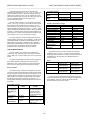
SERIES IP320A INDUSTRIAL I/O PACK 12-BIT HIGH DENSITY ANALOG INPUT BOARD ___________________________________________________________________________________________ Table 3.3: Maximum Overall Uncalibrated Error at 25°C Max Max ADC Offset Gain Input Range PGA Range Error Error (Volts) Gain (Volts) (±LSB) (±LSB ) -5 to +5 1 -5 to +5 1.43 22.53 -2.5 to +2.5 2 " “ " -1.25 to +1.25 4 " “ " -0.625 to 8 " “ " +0.625 -10 to +10 1 -10 to +10 0.72 " -5 to +5 2 " “ " -2.5 to +2.5 4 " “ " -1.25 to +1.25 8 " “ " 0 to +10 1 0 to +10 3.08 24.58 0 to +5 2 " “ " 0 to +2.5 4 " “ " 0 to +1.25 8 " “ " Table 3.4: Recommended Calib. Voltages For Input Ranges Rec. High Rec. Low ADC Calib. Calib. Input Voltage Voltage Range Range PGA "VoltCALHI" "VoltCALLO" (Volts) Gain (Volts) (Volts) (Volts) -5 to 1 -5 to +5 0.0000 (A. Z.) 4.9000 (CAL0) +5 -2.5 to 2 " " 2.4500 (CAL1) +2.5 -1.25 to 4 " " 1.2250 (CAL2) +1.25 -0.625 to 8 " " 0.6125 (CAL3) +0.625 -10 to 1 -10 to " 4.9000 (CAL0) +10 +10 -5 to 2 " " 4.9000 (CAL0) +5 -2.5 to 4 " " 2.4500 (CAL1) +2.5 -1.25 to 8 " " 1.2250 (CAL2) +1.25 0 to 1 0 to +10 0.6125 (CAL3) 4.9000 (CAL0) +10 0 to 2 " " 4.9000 (CAL0) +5 0 to 4 " " 2.4500 (CAL1) +2.5 0 to 8 " " 1.2250 (CAL2) +1.25 Note that the worst case non-linearity error is ±0.75 LSB (the sum of the ½ LSB non-linearity of the ADC and the ¼ LSB non-linearity of the PGA). Calibrated Performance Very accurate calibration of the IP320A can be accomplished by using calibration voltages present on the board. The four voltages and the analog ground reference are used to determine the endpoints of a straight line which defines the analog input characteristic. The calibration voltages are precisely adjusted at the factory to provide optimum performance, as detailed in the following table: The following equation (1) is used to correct the actual ADC data (i.e. the uncorrected bit count read from the ADC) making use of the calibration voltages and range constants. Ideal Maximum Maximum Calibration Value Tolerance Temperature Signal (Volts) @25oC (Volts) Drift (ppm/oC) Auto Zero 0.0000 ±0.0002 0 CAL0 4.9000 ±0.0005 ±15 CAL1 2.4500 ±0.0005 ±20* CAL2 1.2250 ±0.0004 " CAL3 0.6125 ±0.0002 " * Worst case temperature drift is the sum of the ±15 ppm/oC drift of the calibration voltage reference plus the ±5 ppm/oC drift of the resistors in the voltage divider. Corrected_Count = Count_Actu (Volt al + 4096 ∗ m Ideal_Volt_Span * CALLO * Gain) - Ideal_Zero m − Count CALLO (1) where, "m" represents the actual slope of the transfer characteristic as defined in equation 2: Volt CALHI − Volt CALLO Count CALHI − Count CALLO m = Gain ∗ The calibration voltages are used with the auto zero signal to find two points that determine the straight line characteristic of the analog front end for a particular range. The recommended calibration voltage selection for each range is summarized in the following table: - 10 - Gain = VoltCALHI = VoltCALLO = CountCALHI = CountCALLO = Ideal_Volt_Span = (2) The Programmable Gain Amplifier Setting Used (See Table 3.7) High Calibration Voltage (See Table 3.7) Low Calibration Voltage (See Table 3.7) Actual ADC Data Read With High Calibration Voltage Applied Actual ADC Data Read With Low Calibration Voltage Applied Ideal ADC Voltage Span (See Table 3.8)