1
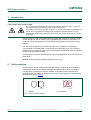
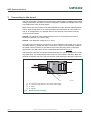
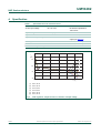
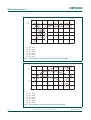
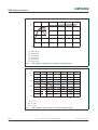
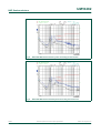
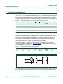
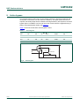
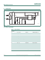
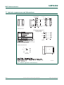
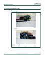
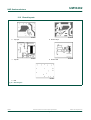
UM10482 SSL21081 LED driver reference board Rev. 2.1 — 11 January 2012 User manual Document information Info Content Keywords SSL21081, buck converter, reference board, LED driver, LED retrofit lamp, low power Abstract This document describes the performance, technical data and connection of the SSL21081 reference board. The SSL2108X series is an NXP Semiconductors driver IC intended to provide a low cost, small form factor LED driver. This board is intended to operate at 100 V (AC) or 120 V (AC), using an output voltage greater than 30 V. UM10482 NXP Semiconductors SSL21081 LED driver reference board Revision history Rev Date Description v.2.1 20120111 fourth issue • Modifications: v.2 20111205 Figure 13 on page 14: 700 H changed to 1 mH. third issue • Modifications: Minor text modifications. v.1.1 20110830 second issue v.1 20110818 first issue Contact information For more information, please visit: http://www.nxp.com For sales office addresses, please send an email to: [email protected] UM10482 User manual All information provided in this document is subject to legal disclaimers. Rev. 2.1 — 11 January 2012 © NXP B.V. 2012. All rights reserved. 2 of 18 UM10482 NXP Semiconductors SSL21081 LED driver reference board 1. Introduction WARNING Lethal voltage and fire ignition hazard The non-insulated high voltages that are present when operating this product, constitute a risk of electric shock, personal injury, death and/or ignition of fire. This product is intended for evaluation purposes only. It shall be operated in a designated test area by personnel qualified according to local requirements and labor laws to work with non-insulated mains voltages and high-voltage circuits. This product shall never be operated unattended. The SSL21081 is a highly integrated switching mode LED driver which enables constant current driving from the AC mains input in a standard SO8 package. It is a solution for small LED retrofit lamp applications, especially those applications for low-power factor designs. The SSL21081 supports buck converter topology and is suitable for non-isolated, non-dimmable LED retrofit lamps. It can drive a long LED string, up to a 70 V forward voltage and is most efficient in this type of LED module. The SSL2108 series is intended to operate at high output voltages. This reference board is an example that can be used in applications up to E17 form factor lamp fittings. Remark: Unless otherwise stated all voltages are in V (AC). 2. Safety warning This reference board is connected to a high AC voltage. Avoid touching the reference board during operation. An isolated housing is mandatory when used in uncontrolled, non-laboratory environments. Galvanic isolation of the mains phase using a fixed or variable transformer (Variac) is always recommended. These devices are recognized by the symbols shown in Figure 1 019aab174 019aab173 a. Isolated Fig 1. UM10482 User manual b. Not isolated Variac isolation symbols All information provided in this document is subject to legal disclaimers. Rev. 2.1 — 11 January 2012 © NXP B.V. 2012. All rights reserved. 3 of 18 UM10482 NXP Semiconductors SSL21081 LED driver reference board 3. Connecting to the board The reference board is optimized for a 100 V/60 Hz mains supply. In addition to the mains voltage optimization, the reference board is designed to operate with multiple LEDs or an LED module with a high forward voltage. Mains connection of this reference board is different from other general evaluation/demo boards. Connect the mains to an axial lead resistor and fuse which are connected to J1 and J2. In the application, it is possible that one side of these components is directly connected to the socket. Remark: The maximum rated voltage of the board is 141 V (limited by the value of electrolytic capacitor C1) or 200 V (DC). Remark: The rated fuse voltage for F1 is 125 V. An anode of the LED string is connected to J3 and a cathode is connected to J4. Use an LED string with a VF greater than 20 V on this board. Under normal operating conditions, the output current is 100 mA. If the rated current of the LED string does not meet the specification, the LED output current is adjusted as described in Section 5. The electrolytic capacitor is mounted outside the board so it can be mounted in the screw cap of the lamp. The temperature around screw cap is the lowest in the lamp. When the capacitor is placed in the screw cap, the life time of the electrolytic capacitor is improved. J4 J3 J2 J1 019aac531 (1) J2: connect the flying lead end of R1 to the AC mains supply. (2) J1: connect the flying lead end of F1 to the AC mains supply. (3) J3: Anode. (4) J4: Cathode. Fig 2. UM10482 User manual Board connection diagram All information provided in this document is subject to legal disclaimers. Rev. 2.1 — 11 January 2012 © NXP B.V. 2012. All rights reserved. 4 of 18 UM10482 NXP Semiconductors SSL21081 LED driver reference board 4. Specification Table 1. Specifications for the reference board Parameter Value Comment AC line input voltage 85 V to 138 V the board is optimized for 100 V/60 Hz. output voltage > 20 V (DC) - output current 100 mA at 100 V mains; 70 V LED output current dependency 5 % 100 V 10 % at 70 V; 100 mA output (see Figure 4) efficiency > 90 % at 70 V; 100 mA output power factor 0.6 at 70 V; 100 mA output board dimension (L W H) 22 mm 18 mm 12 mm - 019aac532 200 Io (mA) 160 (1) (2) (3) (4) 120 (5) (6) 80 40 0 40 80 120 Vo (V) (1) 100 V; 50 Hz. (2) 100 V; 60 Hz. (3) 110 V; 50 Hz. (4) 110 V; 60 Hz. (5) 120 V; 50 Hz. (6) 120 V; 60 Hz. Fig 3. UM10482 User manual Load regulation: output current as a function of output voltage All information provided in this document is subject to legal disclaimers. Rev. 2.1 — 11 January 2012 © NXP B.V. 2012. All rights reserved. 5 of 18 UM10482 NXP Semiconductors SSL21081 LED driver reference board 019aac533 115 Io (mA) 95 (1) (2) 75 (3) (4) (5) (6) 55 65 85 105 125 145 Vi (AC) (1) 35 V; 50 Hz (2) 35 V; 60 Hz (3) 48 V; 60 Hz (4) 48 V; 50 Hz (5) 70 V; 60 Hz (6) 70 V; 50 Hz Fig 4. Line regulation: output current as a function of input voltage 019aac535 93 η (%) (1) (2) 91 (3) 89 (4) (5) (6) 87 65 85 105 125 145 Vi (V) (1) 70 V; 50 Hz. (2) 70 V; 60 Hz. (3) 48 V; 50 Hz. (4) 48 V; 60 Hz. (5) 35 V; 50 Hz. (6) 35 V; 60 Hz. Fig 5. UM10482 User manual Line regulation: efficiency as a function of input voltage All information provided in this document is subject to legal disclaimers. Rev. 2.1 — 11 January 2012 © NXP B.V. 2012. All rights reserved. 6 of 18 UM10482 NXP Semiconductors SSL21081 LED driver reference board 019aac534 100 η (%) (1) 80 (2) (3) (4) (5) (6) 60 40 0 40 80 120 Vo (V) (1) 100 V; 50 Hz. (2) 100 V; 60 Hz. (3) 110 V; 50 Hz. (4) 110 V; 60 Hz. (5) 120 V; 50 Hz. (6) 120 V; 60 Hz. Fig 6. Load regulation: efficiency as a function of output voltage 019aac536 0.75 PF 0.70 0.65 0.60 (1) 0.55 (2) (3) 0.50 70 80 90 100 110 120 130 140 Vi (V) (1) Vo = 70 V (2) Vo = 48 V (3) Vo = 35 V Fig 7. UM10482 User manual Load regulation: power factor as a function of input voltage All information provided in this document is subject to legal disclaimers. Rev. 2.1 — 11 January 2012 © NXP B.V. 2012. All rights reserved. 7 of 18 UM10482 NXP Semiconductors SSL21081 LED driver reference board UM10482 User manual Fig 8. SSL21082 EMC measurement L-phase according to FCC15 norm Fig 9. SSL21082 EMC measurement N-phase according to FCC15 norm All information provided in this document is subject to legal disclaimers. Rev. 2.1 — 11 January 2012 © NXP B.V. 2012. All rights reserved. 8 of 18 UM10482 NXP Semiconductors SSL21081 LED driver reference board 5. Changing the output current The SSL21081 monitors the charging current in the inductor using the sense resistors R2A and R2B. It controls the internal MOSFET to ensure a constant peak current (Ipeak). In addition, the IC supports valley detection. These features enable a driver to operate in Boundary Conduction Mode (BCM) with valley switching where the average current in the inductor is an output current. The SSL21081 turns off the MOSFET when the voltage on pin SOURCE reaches 500 mV. If resistors R2A/R2B between pin SOURCE and GND are 2 , the peak current is limited to 250 mA (see Equation 1). 0.5 R2A + R2B I peak = ----------------------------------------------R2A R2B (1) When the MOSFET is switched off, inductor L2 is discharged and the current flowing through the inductor is decreased. When the current in the inductor reaches 0 mA, the voltage on pin DRAIN starts to oscillate. The SSL21081 waits for a valley in this oscillation. When the voltage on pin DRAIN reaches it lowest value, the MOSFET is turned on again. The charge time of inductor L2 is calculated with Equation 2: 2 I LED t ch = L2 --------------------------V IN – V LED (2) The discharge time of inductor L2 is calculated using Equation 3: 2 I LED t dch = L2 -------------------V LED (3) When the inductor charges/discharges, a current flows through it. However, there is an effective current when oscillating. Consider the oscillation frequency when adjusting the output current. It can be calculated using Equation 4: 1 f ring = -------------------------------------------------------------------2 L2 C FET C4 (4) The time from the start of oscillation to the first valley is calculated using Equation 5: 1 t ring = ------------------2 f ring (5) The output current is calculated using Equation 6: t ch + t dch 1 I LED = --- I peak -------------------------------------2 t ch + t dch + t ring UM10482 User manual All information provided in this document is subject to legal disclaimers. Rev. 2.1 — 11 January 2012 (6) © NXP B.V. 2012. All rights reserved. 9 of 18 UM10482 NXP Semiconductors SSL21081 LED driver reference board 6. External OverTemperature Protection (OTP) The SSL21081 supports external OTP by adding an external Negative Temperature Coefficient (NTC) thermistor. This feature is delivered by detecting a voltage on pin NTC. The NTC pin has an integrated current source that generates an offset. The resistance of the NTC thermistor is decreased as the temperature increases. When the NTC temperature rises and the voltage on pin NTC falls to below 0.5 V, the SSL21081 lowers the threshold level for detecting peak current in the inductor. Decreasing the peak current in the inductor causes the power consumption in the system to decrease as well. The output current is adjusted to the point where a balance between safety temperature and output current can be retained (thermal management). If the temperature on NTC increases continuously and the voltage on the pin drops below 0.3 V, the SSL21081 starts the NTC time-out timer. If the voltage on pin NTC pin does not drop below 0.2 V within the time-out, the SSL21081 detects an abnormal condition and stops switching. An NTC thermistor can be directly connected to pin NTC. It is also possible to tune the protection temperature by adding resistor in parallel or in series with the NTC. One NTC and one resistor are installed on the reference board. The values of these components can be changed depending on the protection temperature requirement and component availability. UM10482 User manual All information provided in this document is subject to legal disclaimers. Rev. 2.1 — 11 January 2012 © NXP B.V. 2012. All rights reserved. 10 of 18 UM10482 NXP Semiconductors SSL21081 LED driver reference board 7. Power factor adjustment The SSL21081 reference board is designed for a standard operation with a power factor of 0.6 at 100 V. This option offers the highest efficiency. There are two ways of tuning the power factor for higher values. The first option is by increasing the value of R1. A higher R1 value raises the power factor to above 0.7, resulting in additional losses (see Table 2). Table 2. Power factor adjustment - increasing the value of resistor R1 Vi (V) Vo (Vavr) Io (mA) R1 () (%) Power factor THD (%) 100 62.8 127 10 91.5 0.6131 111 100 62.8 127 33 85.0 0.701 90.5 120 62.5 123 68 84.7 0.711 94.2 120 63.1 124 100 81.9 0.75 84.3 120 43.5 129 100 82.7 0.715 95.1 Increasing R1 also results in a lower inrush current enabling the board to be connected to leading-edge phase cut dimmers without damage to the dimmer or lamp (dimmer resistant). This adjustment is not intended for stable operation without flicker or a good dimming range, but is for safety only. Dimension the power rating of R1 to handle peak powers that occur using leading-edge dimmers. This power is between 2 W and 4 W. Alternatively, a thermal link can be made between the onboard NTC and resistor R1, causing the board to turn off at an overtemperature of resistor R1. The second option is to increase power factor is with a valley fill circuit. The basic schematic for this circuit is shown in Figure 10. Table 3 shows the results when using a 10 F capacitor for C2X and C2Y. Table 3. Power factor adjustment - valley fill circuit Vi (V) Vo (Vavr) Io (mA) R1 () (%) Power factor THD (%) 120 42.4 133 120 86.0 0.904 43.8 120 20.9 137 220 82.4 0.908 43.1 C2X R1 C2Y 120 Ω 019aac537 Fig 10. Valley fill circuit The valley fill circuit can only be employed in buck converter mode if the output voltage is below half the peak input voltage. In practice, at 120 V (AC) input it operates up to 50 V (DC) output voltage. UM10482 User manual All information provided in this document is subject to legal disclaimers. Rev. 2.1 — 11 January 2012 © NXP B.V. 2012. All rights reserved. 11 of 18 UM10482 NXP Semiconductors SSL21081 LED driver reference board 8. Active bypass An increased value for the inrush current resistor protects the board from damage with most phase cut dimmers, but also lowers the efficiency. If a higher power factor is not required, but leading-edge dimmer resistance and high efficiency are important, the active bypass option is available. In this circuit, the inrush current resistor is bypassed using a Silicon Controlled Rectifier (SCR); see Figure 11. Table 4 shows the results when active bypass is used. Table 4. Active bypass Vi (V) Vo (Vavr) Io (mA) R1 () (%) Power factor THD (%) 100 22 143 56 86.2 0.566 135 100 43 130 56 89.0 0.618 109 120 22 142 56 85.0 0.533 151 120 43 130 56 89.2 0.585 125 1 MΩ 22 nF MCR22-6 56 Ω 019aac538 Fig 11. Active bypass UM10482 User manual All information provided in this document is subject to legal disclaimers. Rev. 2.1 — 11 January 2012 © NXP B.V. 2012. All rights reserved. 12 of 18 UM10482 NXP Semiconductors SSL21081 LED driver reference board 9. Schematic L1 1 J3 LED+ 330 μF U2 S1ZB60 J1 1 VIN1 F1 1A (125 V) 2 C1 8.2 μF (200 V) 3 U1 C2 0.22 μF (250 V) HV SOURCE 4 VCC J2 1 VIN2 C3 0.47 μF (250 V) D1 STTH2R06A 1 R1 NTC 10 Ω 1W R2B 4.7 Ω 1% R2A 4.3 Ω 1% 1 2 8 SSL21081 7 3 6 4 5 L2 DRAIN 1 J4 LED- 1 mH GND2 C4 150 pF (630 V) GND1 DVDT C6 1000 pF RT1 C5 1 μF (25 V) R3 1 kΩ 1% 1608 aaa-000147 Fig 12. Schematic 10. Bill of materials Table 5. Bill of materials Part Qty Values reference UM10482 User manual Manufacturer Part number C1 1 8.2 F; 200 V Rubycon 200BXC10M8X11.5 C2 1 0.22 F; X7R; 250 V Murata RDER72E224K8K1C11B C3 1 0.47 F; X7R; 250 V Murata RDER72E474K5B1C13B C4 1 150 pF; C0G; 603 V Murata GRM31A5C2J151JW01D C5 0 1 F; F; 25 V Murata GRM188F51E105ZA12D C6 1 1000 pF; X7R; 50 V Murata GRM188R71H102KA01D D1 1 600 V; 1 A; fast recovery ST Micro STTH2R06A F1 1 1 A; 125 V Littelfuse 473001 L1 1 330 H Taiyo-Yuden CAL45VB331K L2 1 1 mH TDK-EPC SRL8EE-201V001 R1 1 10 ; 1 W Panasonic ERG-1SJ100A R2A 1 3 ; 1 %; 2012 Dale CRCW08053R00FKEA R2B 1 7.5 ; 1 %; 1608 Dale CRCW06037R50FKEA R3 1 1 k; 1 %; 1608 Panasonic ERJ-3EKF1001V RT1 1 100 k Murata NXFT15WF104FA2B020 U1 1 SSL21081 NXP Semiconductors SSL21081 U2 1 600 V; 0.8 A Shindengen S1ZB60 All information provided in this document is subject to legal disclaimers. Rev. 2.1 — 11 January 2012 © NXP B.V. 2012. All rights reserved. 13 of 18 UM10482 NXP Semiconductors SSL21081 LED driver reference board 11. Inductor appearance and dimensions line edge height 1.5 mm max 2- Ø 0.5 9 max 9 max 9 max 3 4 2 5 1 6 3.3 ± 0.5 Dimensions in mm TERMINAL PIN GAUGE CHECK be able to inserted the gauge as right 1 6 3 4 2.5 ± 0.1 2.5 ± 0.1 6.0 ± 0.1 2- Ø 0.8 WINDING SPECIFICATION 3 core N1 2 N1 primary bottom view aaa-002191 Fig 13. Inductor appearance and dimensions UM10482 User manual All information provided in this document is subject to legal disclaimers. Rev. 2.1 — 11 January 2012 © NXP B.V. 2012. All rights reserved. 14 of 18 UM10482 NXP Semiconductors SSL21081 LED driver reference board 12. Printed-Circuit Board (PCB) 12.1 Board photographs a. Top view b. Bottom view Fig 14. SSL21081 reference board photographs UM10482 User manual All information provided in this document is subject to legal disclaimers. Rev. 2.1 — 11 January 2012 © NXP B.V. 2012. All rights reserved. 15 of 18 UM10482 NXP Semiconductors SSL21081 LED driver reference board 12.2 Board layouts a. Top layer b. Bottom layer c. Top silk d. Bottom silk e. Drill Fig 15. Board layout UM10482 User manual All information provided in this document is subject to legal disclaimers. Rev. 2.1 — 11 January 2012 © NXP B.V. 2012. All rights reserved. 16 of 18 UM10482 NXP Semiconductors SSL21081 LED driver reference board 13. Legal information 13.1 Definitions Draft — The document is a draft version only. The content is still under internal review and subject to formal approval, which may result in modifications or additions. NXP Semiconductors does not give any representations or warranties as to the accuracy or completeness of information included herein and shall have no liability for the consequences of use of such information. 13.2 Disclaimers Limited warranty and liability — Information in this document is believed to be accurate and reliable. However, NXP Semiconductors does not give any representations or warranties, expressed or implied, as to the accuracy or completeness of such information and shall have no liability for the consequences of use of such information. NXP Semiconductors takes no responsibility for the content in this document if provided by an information source outside of NXP Semiconductors. In no event shall NXP Semiconductors be liable for any indirect, incidental, punitive, special or consequential damages (including - without limitation - lost profits, lost savings, business interruption, costs related to the removal or replacement of any products or rework charges) whether or not such damages are based on tort (including negligence), warranty, breach of contract or any other legal theory. Notwithstanding any damages that customer might incur for any reason whatsoever, NXP Semiconductors’ aggregate and cumulative liability towards customer for the products described herein shall be limited in accordance with the Terms and conditions of commercial sale of NXP Semiconductors. Right to make changes — NXP Semiconductors reserves the right to make changes to information published in this document, including without limitation specifications and product descriptions, at any time and without notice. This document supersedes and replaces all information supplied prior to the publication hereof. Suitability for use — NXP Semiconductors products are not designed, authorized or warranted to be suitable for use in life support, life-critical or safety-critical systems or equipment, nor in applications where failure or malfunction of an NXP Semiconductors product can reasonably be expected to result in personal injury, death or severe property or environmental damage. NXP Semiconductors and its suppliers accept no liability for inclusion and/or use of NXP Semiconductors products in such equipment or applications and therefore such inclusion and/or use is at the customer’s own risk. Applications — Applications that are described herein for any of these products are for illustrative purposes only. NXP Semiconductors makes no representation or warranty that such applications will be suitable for the specified use without further testing or modification. UM10482 User manual Customers are responsible for the design and operation of their applications and products using NXP Semiconductors products, and NXP Semiconductors accepts no liability for any assistance with applications or customer product design. It is customer’s sole responsibility to determine whether the NXP Semiconductors product is suitable and fit for the customer’s applications and products planned, as well as for the planned application and use of customer’s third party customer(s). Customers should provide appropriate design and operating safeguards to minimize the risks associated with their applications and products. NXP Semiconductors does not accept any liability related to any default, damage, costs or problem which is based on any weakness or default in the customer’s applications or products, or the application or use by customer’s third party customer(s). Customer is responsible for doing all necessary testing for the customer’s applications and products using NXP Semiconductors products in order to avoid a default of the applications and the products or of the application or use by customer’s third party customer(s). NXP does not accept any liability in this respect. Export control — This document as well as the item(s) described herein may be subject to export control regulations. Export might require a prior authorization from competent authorities. Evaluation products — This product is provided on an “as is” and “with all faults” basis for evaluation purposes only. NXP Semiconductors, its affiliates and their suppliers expressly disclaim all warranties, whether express, implied or statutory, including but not limited to the implied warranties of non-infringement, merchantability and fitness for a particular purpose. The entire risk as to the quality, or arising out of the use or performance, of this product remains with customer. In no event shall NXP Semiconductors, its affiliates or their suppliers be liable to customer for any special, indirect, consequential, punitive or incidental damages (including without limitation damages for loss of business, business interruption, loss of use, loss of data or information, and the like) arising out the use of or inability to use the product, whether or not based on tort (including negligence), strict liability, breach of contract, breach of warranty or any other theory, even if advised of the possibility of such damages. Notwithstanding any damages that customer might incur for any reason whatsoever (including without limitation, all damages referenced above and all direct or general damages), the entire liability of NXP Semiconductors, its affiliates and their suppliers and customer’s exclusive remedy for all of the foregoing shall be limited to actual damages incurred by customer based on reasonable reliance up to the greater of the amount actually paid by customer for the product or five dollars (US$5.00). The foregoing limitations, exclusions and disclaimers shall apply to the maximum extent permitted by applicable law, even if any remedy fails of its essential purpose. 13.3 Trademarks Notice: All referenced brands, product names, service names and trademarks are the property of their respective owners. All information provided in this document is subject to legal disclaimers. Rev. 2.1 — 11 January 2012 © NXP B.V. 2012. All rights reserved. 17 of 18 UM10482 NXP Semiconductors SSL21081 LED driver reference board 14. Contents 1 2 3 4 5 6 7 8 9 10 11 12 12.1 12.2 13 13.1 13.2 13.3 14 Introduction . . . . . . . . . . . . . . . . . . . . . . . . . . . . 3 Safety warning . . . . . . . . . . . . . . . . . . . . . . . . . . 3 Connecting to the board . . . . . . . . . . . . . . . . . . 4 Specification. . . . . . . . . . . . . . . . . . . . . . . . . . . . 5 Changing the output current . . . . . . . . . . . . . . 9 External OverTemperature Protection (OTP) 10 Power factor adjustment . . . . . . . . . . . . . . . . . 11 Active bypass. . . . . . . . . . . . . . . . . . . . . . . . . . 12 Schematic . . . . . . . . . . . . . . . . . . . . . . . . . . . . . 13 Bill of materials . . . . . . . . . . . . . . . . . . . . . . . . 13 Inductor appearance and dimensions . . . . . . 14 Printed-Circuit Board (PCB) . . . . . . . . . . . . . . 15 Board photographs . . . . . . . . . . . . . . . . . . . . . 15 Board layouts . . . . . . . . . . . . . . . . . . . . . . . . . 16 Legal information. . . . . . . . . . . . . . . . . . . . . . . 17 Definitions . . . . . . . . . . . . . . . . . . . . . . . . . . . . 17 Disclaimers . . . . . . . . . . . . . . . . . . . . . . . . . . . 17 Trademarks. . . . . . . . . . . . . . . . . . . . . . . . . . . 17 Contents . . . . . . . . . . . . . . . . . . . . . . . . . . . . . . 18 Please be aware that important notices concerning this document and the product(s) described herein, have been included in section ‘Legal information’. © NXP B.V. 2012. All rights reserved. For more information, please visit: http://www.nxp.com For sales office addresses, please send an email to: [email protected] Date of release: 11 January 2012 Document identifier: UM10482