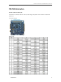
1
Xtreme I/O ADC-DAC User Manual Connect Tech Inc. 42 Arrow Road Guelph, Ontario N1K 1S6 Tel: Toll: Fax: Email: Web: 519-836-1291 800-426-8979 (North America only) 519-836-4878 [email protected] [email protected] www.connecttech.com CTIM-00092 Revision 0.02 – 12/09/2014 Connect Tech Xtreme I/O ADC-DAC Family User Manual Limited Lifetime Warranty Connect Tech Inc. provides a lifetime warranty for all of our products. Should this product, in Connect Tech Inc.’s opinion, fail to be in good working order during the warranty period, Connect Tech Inc. will, at its option, repair or replace this product at no charge, provided that the product has not been subjected to abuse, misuse, accident, disaster or non Connect Tech Inc. authorized modification or repair. You may obtain warranty service by delivering this product to an authorized Connect Tech Inc. business partner or directly to Connect Tech Inc. along with proof of purchase. Product returned to Connect Tech Inc. must be pre-authorized by Connect Tech Inc. with an RMA (Return Material Authorization) number marked on the outside of the package and sent prepaid, insured and packaged for safe shipment. Connect Tech Inc. will return this product by prepaid ground shipment service. The Connect Tech Inc. lifetime warranty is defined as the serviceable life of the product. This is defined as the period during which all components are available. Should the product prove to be irreparable, Connect Tech Inc. reserves the right to substitute an equivalent product if available or to retract lifetime warranty if no replacement is available. The above warranty is the only warranty authorized by Connect Tech Inc. Under no circumstances will Connect Tech Inc. be liable in any way for any damages, including any lost profits, lost savings or other incidental or consequential damages arising out of the use of, or inability to use, such product. Copyright Notice The information contained in this document is subject to change without notice. Connect Tech Inc. shall not be liable for errors contained herein or for incidental consequential damages in connection with the furnishing, performance, or use of this material. This document contains proprietary information that is protected by copyright. All rights are reserved. No part of this document may be photocopied, reproduced, or translated to another language without the prior written consent of Connect Tech Inc. Copyright 2012 by Connect Tech Inc. Trademark Acknowledgment Connect Tech Inc. acknowledges all trademarks, registered trademarks and/or copyrights referred to in this document as the property of their respective owners. Not listing all possible trademarks or copyright acknowledgments does not constitute a lack of acknowledgment to the rightful owners of the trademarks and copyrights mentioned in this document. 2 Revision 0.02 Connect Tech Xtreme I/O ADC-DAC User Manual Table of Contents Limited Lifetime Warranty ............................................................................................................................................... 2 Copyright Notice............................................................................................................................................................... 2 Trademark Acknowledgment ............................................................................................................................................ 2 Table of Contents .............................................................................................................................................................. 3 Revision History ............................................................................................................................................................... 3 Customer Support Overview ............................................................................................................................................. 4 Contact Information .......................................................................................................................................................... 4 Introduction....................................................................................................................................................................... 5 Product Features ............................................................................................................................................................... 5 Board Diagram.................................................................................................................................................................. 6 Block Diagram .................................................................................................................................................................. 7 Part Number Information .................................................................................................................................................. 8 Analog Inputs (ADC’s) ..................................................................................................................................................... 9 Overview ............................................................................................................................................. 9 ADC Connector (P4) Pinout .................................................................................................................. 9 ADC Operation .................................................................................................................................. 10 Analog Outputs (DAC’s) .................................................................................................................................................12 Overview ........................................................................................................................................... 12 DAC Connector (P7) Pinout ................................................................................................................ 12 DAC Operation .................................................................................................................................. 13 GPIO (Digital I/O) ...........................................................................................................................................................15 Overview ........................................................................................................................................... 15 GPIO Connector (P3) Pinout .............................................................................................................. 15 GPIO Operation ................................................................................................................................ 16 PCI-104 Information ........................................................................................................................................................17 LED Indicators.................................................................................................................................................................19 Device Software / Configuration Information..................................................................................................................20 PCI Device Information ...................................................................................................................... 20 Device Register Description (Memory Map) ......................................................................................... 20 Memory Map Detailed View ................................................................................................................ 21 FPGA Custom Configuration...........................................................................................................................................22 Revision History Revision Date Author(s) Change(s) 0.00 01-03-2012 PD Initial Manual Revision Created 0.01 03-14-2013 PD - Fixed DAC Pseudo Code Examples - Fixed GPIO Register Diagram - Added Power Details for Input Power and Current Consumption 0.02 12-09-2014 PD - Corrected PCI IDs (all should be 0x1201) Revision 0.02 3 Connect Tech Xtreme I/O ADC-DAC Family User Manual Customer Support Overview If you experience difficulties after reading the manual and/or using the product, contact the Connect Tech Inc. reseller from which you purchased the product. In most cases the reseller can help you with product installation and difficulties. In the event that the reseller is unable to resolve your problem, our highly qualified support staff can assist you. Our support section is available 24 hours a day, 7 days a week on our website at: www.connecttech.com/sub/support/support.asp. See the contact information section below for more information on how to contact us directly. Our technical support is always free. Contact Information We offer three ways for you to contact us: Mail/Courier You may contact us by letter at: Connect Tech Inc. Technical Support 42 Arrow Road, Guelph, ON Canada N1K 1S6 Email/Internet You may contact us through the Internet. Our email and URL addresses on the Internet are: [email protected] [email protected] www.connecttech.com Note: Please go to the Download Zone or the Knowledge Database in the Support Center on the Connect Tech Inc. website for product manuals, installation guides, device driver software and technical tips. Submit your technical support questions to our customer support engineers via the Support Center on the Connect Tech Inc. website. Telephone/Facsimile Technical Support representatives are ready to answer your call Monday through Friday, from 8:30 a.m. to 5:00 p.m. Eastern Standard Time. Our numbers for calls are: Telephone: Telephone: Facsimile: 4 800-426-8979 (North America only) 519-836-1291 (Live assistance available 8:30 a.m. to 5:00 p.m. EST, Monday to Friday) 519-836-4878 (online 24 hours) Revision 0.02 Connect Tech Xtreme I/O ADC-DAC User Manual Introduction Connect Tech’s Xtreme I/O ADC-DAC is an analog and digital peripheral board for the PCI-104 small form factor embedded marketplace. This product is ideal for data acquisition, measurement and control applications. Product Specifcations Specification Details Form Factor PCI-104 or PC/104-Plus Fully PCI 2.0 bus compliant Jumpers not required for configuration or board detection Analog Inputs Channels: 32 Single Ended / 16 Differential Resolution: o DAG003: 16-bit o DAG004: 16-bit o DAG005: 12-bit (low cost option) Sampling Rate: 100ksps Calibration: Built in temperature Auto calibration Protection: ±25V Input Ranges: Software-Programmable Input Ranges: o 0-5V, 0-10V, ±5V, ±10V Temperature Range: 1LSB INL and DNL over: o -40ºC to 85ºC (-40ºF to 185ºF) Signal-to-Noise Ratio: 87dB Analog Outputs Channels: 4 Resolution: 16-bit Output Ranges: Six Programmable Output Ranges o Unipolar: 0V to 5V, 0V to 10V o Bipolar: ±5V, ±10V, ±2.5V, –2.5V to 7.5V Temperature Range: 1LSB INL and DNL over full -40ºC to 85ºC (-40ºF to 185ºF) Outputs Drive: ±5mA Digital I/O Channels: 16-bit bidirectional I/O Input/Output Ranges: Hardware selectable +3.3V or +5V(TTL/CMOS) Output Drive: High Current 24mA Controller FPGA Register Controlled Device (No jumpers needed) Custom logic available upon request Operating Temperature -40 to +85 Degrees Celsius Dimensions 3.775” x 3.550” (PC/104 Compliant) Host Interface Bus PCI-104 (PC/104-Plus) ISA (PC/104) connector can be optionally installed as a pass-through connector Power Details +5VDC only operation (all on-board voltages are made from the +5V rail) Current Consumption (800mA peak, 500mA typical) Software Compatibility Custom CTI Device Drivers for QNX, Linux, Windows Device can also be controlled directly from a memory mapped register set in any operating system Warranty and Support Lifetime Warranty Free Technical Support Revision 0.02 5 Connect Tech Xtreme I/O ADC-DAC Family User Manual Board Diagram 6 Revision 0.02 Connect Tech Xtreme I/O ADC-DAC User Manual Block Diagram Revision 0.02 7 Connect Tech Xtreme I/O ADC-DAC Family User Manual Part Number Information Part Number Features DAG003 Analog Inputs : 16-bit 32 SE / 16 Diff Analog Outputs : 16-bit 4 Channels GPIO : 16-bits DAG004 Analog Inputs : 16-bit 32 SE / 16 Diff Analog Outputs : None GPIO : 16-bits DAG005 Analog Inputs : 12-bit 32 SE / 16 Diff Analog Outputs : None GPIO : 16-bits Board Image Other available ordering options: PC/104 pass-through connector installed Vertical pin-headers installed PCI-104 ID Selection jumpers installed instead of rotary switch GPIO removed completely ADC inputs scalable from 32 SE / 16 Diff (max) to 8 SE / 4 Diff (min) To order any of these part numbers or to inquire about the other available ordering options please contact [email protected] for further information. 8 Revision 0.02 Connect Tech Xtreme I/O ADC-DAC User Manual Analog Inputs (ADC’s) Overview The Xtreme I/O ADC-DAC use 4 ADC IC’s which are interfaced to the on-board FPGA. Each of these ADC IC’s have an 8-channel multiplexer that allow for the sampling of 8 single ended channels or 4 differential channels. ADC IC Features and Specifications Part Number: LTC1859 (DAG003, DAG004) LTC1857 (DAG005) Resolution: 16-bit (DAG003, DAG004) 12-Bit (DAG005) Sample Rate: 100ksps 8-Channel Multiplexer with ±25V Protection Software-Programmable Input Ranges: 0V to 5V, 0V to 10V, ±5V or ±10V Single Ended or Differential ±3LSB INL for the DAG003 & DAG004, ±1LSB INL for the DAG005 Power Dissipation: 40mW (Typ) Signal-to-Noise Ratio: 87dB (Typ) for the LTC1859 The ADC IC datasheet can be found here: http://cds.linear.com/docs/Datasheet/185789fa.pdf ADC Connector (P4) Pinout Pinout Table Signal ADC0 SE-CH0 / DIFF-CH0+ ADC0 SE-CH2 / DIFF-CH1+ ADC0 SE-CH4 / DIFF-CH2+ ADC0 SE-CH6 / DIFF-CH3+ GND ADC1 SE-CH0 / DIFF-CH0+ ADC1 SE-CH2 / DIFF-CH1+ ADC1 SE-CH4 / DIFF-CH2+ ADC1 SE-CH6 / DIFF-CH3+ GND ADC2 SE-CH0 / DIFF-CH0+ ADC2 SE-CH2 / DIFF-CH1+ ADC2 SE-CH4 / DIFF-CH2+ ADC2 SE-CH6 / DIFF-CH3+ GND ADC3 SE-CH0 / DIFF-CH0+ ADC3 SE-CH2 / DIFF-CH1+ ADC3 SE-CH4 / DIFF-CH2+ ADC3 SE-CH6 / DIFF-CH3+ GND Connector Location HDR Pin 1 3 5 7 9 11 13 15 17 19 21 23 25 27 29 31 33 35 37 39 HDR Pin 2 4 6 8 10 12 14 16 18 20 22 24 26 28 30 32 34 36 38 40 Signal ADC0 SE-CH1 / DIFF-CH0ADC0 SE-CH3 / DIFF-CH1ADC0 SE-CH5 / DIFF-CH2ADC0 SE-CH7 / DIFF-CH3GND ADC1 SE-CH1 / DIFF-CH0ADC1 SE-CH3 / DIFF-CH1ADC1 SE-CH5 / DIFF-CH2ADC1 SE-CH7 / DIFF-CH3GND ADC2 SE-CH1 / DIFF-CH0ADC2 SE-CH3 / DIFF-CH1ADC2 SE-CH5 / DIFF-CH2ADC2 SE-CH7 / DIFF-CH3GND ADC3 SE-CH1 / DIFF-CH0ADC3 SE-CH3 / DIFF-CH1ADC3 SE-CH5 / DIFF-CH2ADC3 SE-CH7 / DIFF-CH3GND Pinout Diagram (“Right” Side View of Board) Revision 0.02 9 Connect Tech Xtreme I/O ADC-DAC Family User Manual ADC Operation For each ADC IC the selection of the channel to be sampled, single vs. different and the input voltage range are all configured through an 8-bit command. Each of these commands is stored in an ADC Command register at byte offsets 0x08 for ADC0, 0x09 for ADC1, 0x0A for ADC2 and 0x0B for ADC3. Once the Xtreme I/O ADC-DAC is powered on it continually sends these commands out to the ADC IC’s and samples/stores their 16-bit (or 12-bit) codes in 16-bit registers at byte offsets 0x00 for ADC0, 0x02 for ADC1, 0x04 for ADC2 and 0x06 for ADC3. Please refer to the complete memory map table in Section X for more details. ADC Configuration Commands Each 8-bit ADC command has the following bit layout: SGL/DIFF# 7 ODD SIGN 6 SELECT 5 INPUT RANGE 3 2 4 ZEROS 1 0 The parameters for the ADC commands are described below: MUX ADDRESS SGL/DIFF# ODD SIGN SELECT 0 0 0 0 0 0 0 1 0 0 1 0 0 0 1 1 0 1 0 0 0 1 0 1 0 1 1 0 0 1 1 1 1 0 0 0 1 0 0 1 1 0 1 0 1 0 1 1 1 1 0 0 1 1 0 1 1 1 1 0 1 1 1 1 0 + 1 - 2 + CHANNEL SELECTION 3 4 6 7 + - - + + - 5 - + - + - + + + + + + + + + Note: Single ended readings are referenced to the GND pins on the P4 connector. Input Range Details UNI 0 0 1 1 GAIN 0 1 0 1 INPUT RANGE -5V to +5V -10V to +10V 0V to +5V 0V to +10V ADC Code Conversions When reading the samples from the ADC’s on the Xtreme I/O ADC-DAC, they will be 16-bit codes of natural binary format with 1LSB = SCALE/65536. Code translation examples: Code = 0000 0000 0000 0000 | Scale = 0 to +5V = 5 | Therefore sampled Voltage is = 0.0000V Code = 1000 0000 0000 0000 | Scale = 0 to +5V = 5 | Therefore sampled Voltage is = 2.5000V Code = 1111 1111 1111 1111 | Scale = 0 to +5V = 5 | Therefore sampled Voltage is = 4.9999V Code = 0000 0000 0000 0000 | Scale = 0 to +10V = 10 | Therefore sampled Voltage is = 0.0000V Code = 1000 0000 0000 0000 | Scale = 0 to +10V = 10 | Therefore sampled Voltage is = 5.0000V Code = 1111 1111 1111 1111 | Scale = 0 to +10V = 10 | Therefore sampled Voltage is = 9.9999V Code = 0000 0000 0000 0000 | Scale = -5 to +5V = 10 | Therefore sampled Voltage is = -4.9999V Code = 1000 0000 0000 0000 | Scale = -10 to +10V = 20 | Therefore sampled Voltage is = 0.0000V 10 Revision 0.02 Connect Tech Xtreme I/O ADC-DAC User Manual ADC Operation Pseudo Code Example A In this example we will set all 4 ADC’s to take a single ended readings from SE-CH0 with an input voltage range of 0 to +10V and then we will read back the values //setup command registers write DWord 0x8C8C8C8C to //read from ADC0 ADC0code = read Word from //read from ADC1 ADC1code = read Word from //read from ADC2 ADC2code = read Word from //read from ADC3 ADC3code = read Word from //you can now continually offset 0x08 offset 0x00 offset 0x02 offset 0x04 offset 0x06 do as many reads as you would like ADC Operation Pseudo Code Example B In this example we will set: - ADC0 to take a differential readings from DIFF-CH1 with an input voltage range of -5V to +5V - ADC1 to take a single ended readings from CH6 with an input voltage range of 0V to +5V - ADC2 to take a differential readings from DIFF-CH0 with an input voltage range of -10V to +10V - ADC3 to take a single ended readings from CH2 with an input voltage range of -10V to +10V Then every 500ms we will store a sample. //setup command registers write DWord 0x9404B810 to offset 0x08 //start loop loop //read from ADC0 ADC0code = read Word //read from ADC1 ADC1code = read Word //read from ADC2 ADC2code = read Word //read from ADC3 ADC3code = read Word wait 500ms end loop from offset 0x00 from offset 0x02 from offset 0x04 from offset 0x06 Custom ADC Operation Configuration As stated the current shipping configuration of the Xtreme I/O ADC-DAC is setup for a continuous sampling mode. If your end application requires other functionality such as: - Onboard Hardware buffering or a particular sample size - PCI interrupts generated from the board based on a specific sample range or other criteria - Other functionality not mentioned Please contact Connect Tech Technical Support ([email protected]) to request a custom configuration and CTI engineering team would be happy to help design a customer configuration for you very quickly. Revision 0.02 11 Connect Tech Xtreme I/O ADC-DAC Family User Manual Analog Outputs (DAC’s) Overview The Xtreme I/O ADC-DAC uses a 16-bit 4-channel DAC IC which is interfaced to the on-board FPGA. Each of the 4 analog output channels from the DAC can be controlled independently from the DAC command register at offset 0x18 (the DAC Command register is 32-bits wide). DAC IC Features and Specifications Part Number: LTC2704 (DAG003) Six Programmable Output Ranges: o Unipolar: 0V to 5V, 0V to 10V o Bipolar: ±5V, ±10V, ±2.5V, –2.5V to 7.5V 1LSB INL and DNL Over the Industrial Glitch Impulse: < 2nV-sec Outputs Drive ±5mA Settling Time: 4us min, 10us max (in worst case +/-10V range) Power-On and Clear to Zero Volts The DAC IC datasheet can be found here: http://cds.linear.com/docs/Datasheet/2704fc.pdf DAC Connector (P7) Pinout Pinout Table Signal DAC_OUTA DAC_OUTB DAC_OUTC DAC_OUTD GND Connector Location HDR Pin 1 3 5 7 9 HDR Pin 2 4 6 8 10 Signal GND GND GND GND GND Pinout Diagram (“Left” Side View of Board) 12 Revision 0.02 Connect Tech Xtreme I/O ADC-DAC User Manual DAC Operation The DAC is controlled directly from a 32-bit DWord DAC command register located at offset 0x18. This command register has two main functions, setting the span value and setting DAC code. Each DAC channel will hold buffer and hold its value until the same DAC is written to again. The command register is described in detail below: DAC Command Register (offset 0x18) Zeros Control Address DAC Code or Span 31 30 29 28 27 26 25 24 23 22 21 20 19 18 17 16 15 14 13 12 11 10 9 8 7 6 5 Control 0 1 1 0 1 1 1 0 0 1 0 0 0 1 0 1 Write Span to DAC n Write Code to DAC n Write Span to all DACs Write Code to all DACs Address 0 0 0 0 0 1 0 1 0 0 1 1 1 1 1 0 0 0 0 1 DAC A DAC B DAC C DAC D All Dacs Span 0 0 0 0 0 0 0 0 0 0 0 0 0 0 0 0 0 0 0 0 0 0 0 0 0 0 0 0 0 0 0 0 0 0 0 0 0 0 0 0 0 0 0 0 0 0 0 0 0 0 0 0 0 0 0 0 0 0 0 0 0 0 0 0 0 0 0 0 0 0 0 0 0 0 0 0 0 0 0 0 0 0 1 1 0 0 1 1 0 0 0 1 0 1 0 1 4 3 2 1 0 0V to 5V 0V to 10V -5V to 5V -10 to 10V -2.5V to 2.5V -2.5 to 7.5V DAC Code Conversions When setting the various DAC output voltages for the DAC on the Xtreme I/O ADC-DAC, they will be 16bit codes of natural binary format with 1LSB = SPAN/65536. Code translation examples: Code = 0000 0000 0000 0000 | SPAN = 0V to +10V = 10 | Therefore output voltage will be = 0.0000V Code = 1000 0000 0000 0000 | SPAN = 0V to +10V = 10 | Therefore output voltage will be = 5.0000V Code = 1111 1111 1111 1111 | SPAN = 0V to +10V = 10 | Therefore output voltage will be = 9.9999V Code = 0000 0000 0000 0000 | SPAN = -2.5V to +2.5V = 5 | Therefore output voltage will be = -2.4999V Code = 1000 0000 0000 0000 | SPAN = -2.5V to +2.5V = 5 | Therefore output voltage will be = 0.0000V Code = 1111 1111 1111 1111 | SPAN = -2.5V to +2.5V = 5 | Therefore output voltage will be = 2.4999V Code = 0000 0000 0000 0000 | SPAN = 0V to +5V = 5 | Therefore output voltage will be = 1.2500V Code = 0100 0000 0000 0000 | SPAN = 0V to +5V = 5 | Therefore output voltage will be = 2.5000V Code = 1111 1111 1111 1111 | SPAN = 0V to +5V = 5 | Therefore output voltage will be = 4.9999V Revision 0.02 13 Connect Tech Xtreme I/O ADC-DAC Family User Manual DAC Operation Pseudo Code Example A In this example we will set all 4 DAC’s to have a span voltage range of 0 to +10V and then set all DAC channel outputs to +10V. //setup span write DWord 0x008F0001 to offset 0x18 //set output voltages on all DACs write DWord 0x009FFFFF to offset 0x18 DAC Operation Pseudo Code Example B In this example we will set all 4 DAC’s to have a span voltage range of 0 to +10V and then set DAC_OUTA to +0.625V, DAC_OUTB to +1.25V, DAC_OUTC to +2.5V, DAC_OUTD to +5V. //setup span write DWord 0x008F0001 to //set DAC_OUTA to +0.625V write DWord 0x00701000 to //set DAC_OUTB to +1.25V write DWord 0x00722000 to //set DAC_OUTC to +2.5V write DWord 0x00744000 to //set DAC_OUTD to +5V write DWord 0x00768000 to offset 0x18 offset 0x18 offset 0x18 offset 0x18 offset 0x18 DAC Operation Pseudo Code Example C In this example we will set DACA span to -5V to +5V, DACB span to 0 to +5V, DACC span to -2.5V to +2.5V and DACD span to -10V to +10V. Then we will set DAC_OUTA to 0V, DAC_OUTB to +3.3V, DAC_OUTC to +2.5V, DAC_OUTD to +5V. //set write //set write //set write //set write DACA span to -5V to +5V DWord 0x00600002 to offset 0x18 DACB span to 0V to +5V DWord 0x00620000 to offset 0x18 DACC span to -2.5V to +2.5V DWord 0x00640004 to offset 0x18 DACD span to -10V to +10V DWord 0x00660003 to offset 0x18 //set write //set write //set write //set write DAC_OUTA to +0V DWord 0x00708000 to DAC_OUTB to +3.3V DWord 0x0072A900 to DAC_OUTC to +2.5V DWord 0x0074FFFF to DAC_OUTD to +5V DWord 0x0076C000 to 14 offset 0x18 offset 0x18 offset 0x18 offset 0x18 Revision 0.02 Connect Tech Xtreme I/O ADC-DAC User Manual GPIO (Digital I/O) Overview The Xtreme I/O ADC-DAC has 16-bits of bi-directional GPIO that can be configured to operate with +3.3V or +5V logic levels. The upper and lower 8 bytes (GPIO0–GPIO7 = lower | GPIO8-GPIO15=upper) can be set to either inputs or outputs independently. GPIO Connector (P3) Pinout Pinout Table Signal GPIO0 GPIO2 GPIO4 GPIO6 GPIO8 GPIO10 GPIO12 GPIO14 GND GND GND GND GND Connector Location HDR Pin 1 3 5 7 9 11 13 15 17 19 21 23 25 HDR Pin 2 4 6 8 10 12 14 16 18 20 22 24 26 Signal GPIO1 GPIO3 GPIO5 GPIO7 GPIO9 GPIO11 GPIO13 GPIO15 GND GND GND GND GND Pinout Diagram (“Left” Side View of Board) GPIO Voltage Selection Jumper J2 GPIO VOLTAGE = +5V GPIO VOLTAGE = +3.3V Revision 0.02 15 Connect Tech Xtreme I/O ADC-DAC Family User Manual GPIO Operation The GPIO operation on the Xtreme I/O ADC-DAC is directly controlled via 3 registers: GPIO_OUT, GPIO_IN and GPIO-MISC_CMD. The register GPIO_OUT at offset 0x0C will set the state of any GPIO pins that are set to outputs. The register GPIO_IN at offset 0x10 will contain the current state of any the GPIO pins that are set to inputs. Any pins that are set to outputs will read a zero value. The input/output directions of the GPIO bits are controlled via the GPIO-MISC_CMD register at offset 0x14. GPIO OUTPUT Register (offset 0x0C) GPIO OUTPUT Reserved 31 30 29 28 27 26 25 24 23 22 21 20 19 18 17 16 15 14 13 12 11 10 9 8 7 6 5 4 3 2 1 0 4 3 2 1 0 GPIO INPUT Register (offset 0x10) GPIO INPUT Reserved 31 30 29 28 27 26 25 24 23 22 21 20 19 18 17 16 15 14 13 12 11 10 9 8 7 6 5 Note: Each bit corresponds to the GPIO signal on the connector, IE bit-0 = GPIO0 and bit-9 = GPIO9 GPIO-MISC_CMD Register (offset 0x14) USER LED 31 . . Reserved . . 3 2 GPIO8-15 DIR 1 GPIO0-7 DIR 0 GPIO0-7 or GPIO8-15 = 0 = OUTPUTS GPIO0-7 or GPIO8-15 = 1 = INPUTS GPIO Operation Pseudo Code Example A In this example we will set all the GPIO to outputs and the switch all GPIO signals from low to high. //setup GPIO directions write DWord 0x00000000 to offset 0x14 //set all GPIO signals low write DWord 0x00000000 to offset 0x0C //set all GPIO signals high write DWord 0x0000FFFF to offset 0x0C GPIO Operation Pseudo Code Example B In this example we will set GPIO0-7 as inputs and GPIO8-15 as outputs, then we will read the GPIO inputs. //setup GPIO directions write DWord 0x00000001 to offset 0x14 //read GPIO signals status GPIO inputs = read Word at offset 0x10 16 Revision 0.02 Connect Tech Xtreme I/O ADC-DAC User Manual PCI-104 Information PCI-104 Connector Pinout (P6) Connector P6 is connects to the PCI-104 bus, a full listing of the pinout of the connector is found in the table below. Connector Location Pinout Table Revision 0.02 17 Connect Tech Xtreme I/O ADC-DAC Family User Manual PCI-104 Stack Position Selection The following PCI signals, (INTA#, INTB# INTC# INTD#), (CLK0, CLK1,CLK2, CLK3), (IDSEL0, IDSEL1, IDSEL2, IDSEL3), are selected by using the jumper block or rotary switch (optionally installed) on the Xtreme I/O ADC-DAC board (J1 / RSW1). Selections need to match the stack location of the Xtreme I/O ADC-DAC in your PCI-104 stack. See the table below for more details. Stack Location 18 Rotary Switch Setting Jumper Block Setting PCI INT# PCI CLK PCI IDSEL 0,4,8,C INTA# CLK0 IDSEL0 1,5,9,D INTB# CLK1 IDSEL1 2,6,A,E INTC# CLK2 IDSEL2 3,7,B,F INTD# CLK3 IDSEL3 Revision 0.02 Connect Tech Xtreme I/O ADC-DAC User Manual LED Indicators The Xtreme I/O ADC-DAC has 2 indicator LEDs as shown below. LED D2 is the “heartbeat” indicator, the LED should flash on and off continuously to indicate the Xtreme I/O ADC-DAC is operating properly. LED3 is intended for user configuration and testing and it is directly mapped to GPIO-MISC_CMD register (offset 0x14) Bit 31. D2 – Xtreme I/O ADC-DAC “Heartbeat” D3 – User LED (Mapped to GPIO-MISC_CMD REG Bit 31) If LED D2 is not flashing at all times when the Xtreme I/O ADC-DAC is powered up please contact Connect Tech Technical Support ([email protected]). Revision 0.02 19 Connect Tech Xtreme I/O ADC-DAC Family User Manual Device Software / Configuration Information PCI Device Information The Xtreme I/O ADC-DAC product will have the following properties in a PCI system. PCI Vendor ID: PCI Device ID: PCI Class Code: 0x12C4 0x1201 0x0780 The Xtreme I/O ADC-DAC has a single register bank which is located in the devices BAR 0 location and is occupies 256 bytes of memory space. Below is the output from the lspci utility in Linux with a Xtreme I/O ADC-DAC installed in the system: 00:0d.0 Communication controller [0780]: Connect Tech Inc Device [12c4:1201] (rev 01) Control: I/O- Mem+ BusMaster- SpecCycle- MemWINV- VGASnoop- ParErr- SteppingSERR- FastB2B- DisINTxStatus: Cap+ 66MHz- UDF- FastB2B- ParErr- DEVSEL=slow >TAbort- <TAbort<MAbort- >SERR- <PERR- INTx+ Interrupt: pin A routed to IRQ 18 Region 0: Memory at db020000 (32-bit, non-prefetchable) [size=256] Device Register Description (Memory Map) All of the Xtreme I/O ADC-DAC register control set is memory mapped into BAR0 of the PCI device. There are 8 32-bit registers which are used for control and reading of the Xtreme I/O ADC-DAC board. Each of these registered are described in detail in their respective sections throughout this manual, below is a brief overview of all of the registers. Register Map Overview REGISTER ADC01_DATA ADC23_DATA ADC0123_CMD GPIO_OUT GPIO_IN GPIO-MISC_CMD DAC_CMD RESERVED 20 READ / WRITE R R RW RW R RW RW R OFFSET (HEX) 00 04 08 0C 10 14 18 1C OFFSET (DEC) 0 4 8 12 16 20 24 28 REG NUM 0 1 2 3 4 5 6 7 Revision 0.02 Connect Tech Xtreme I/O ADC-DAC User Manual Memory Map Detailed View Offset 0x00 ADC01_DATA 0x04 ADC23_DATA 0x08 ADC0123_CMD Register Contents ADC0 Code ADC1 Code 31 30 29 28 27 26 25 24 23 22 21 20 19 18 17 16 15 14 13 12 11 10 9 8 7 6 5 4 3 2 1 0 ADC2 Code ADC3 Code 31 30 29 28 27 26 25 24 23 22 21 20 19 18 17 16 15 14 13 12 11 10 9 8 7 6 5 4 3 2 1 0 ADC0 Command 5 4 3 2 1 0 ADC2 Command ADC1 Command ADC3 Command 31 30 29 28 27 26 25 24 23 22 21 20 19 18 17 16 15 14 13 12 11 10 9 8 7 6 GPIO OUTPUT Reserved 31 30 29 28 27 26 25 24 23 22 21 20 19 18 17 16 15 14 13 12 11 10 9 8 7 6 5 4 3 2 1 0 GPIO_IN GPIO INPUT Reserved 31 30 29 28 27 26 25 24 23 22 21 20 19 18 17 16 15 14 13 12 11 10 9 8 7 6 5 4 3 2 1 0 0x14 LED Reserved 31 30 29 28 27 26 25 24 23 22 21 20 19 18 17 16 15 14 13 12 11 10 9 UD LD 5 4 3 2 1 0 Zeros DAC Control DAC Address DAC Code or Span 31 30 29 28 27 26 25 24 23 22 21 20 19 18 17 16 15 14 13 12 11 10 9 8 7 6 5 4 3 2 1 0 Reserved 31 30 29 28 27 26 25 24 23 22 21 20 19 18 17 16 15 14 13 12 11 10 9 4 3 2 1 0 0x0C GPIO_OUT 0x10 GPIO-MISC_CMD 0x18 DAC_CMD 0x1C RESV Revision 0.02 8 8 7 7 6 6 5 21 Connect Tech Xtreme I/O ADC-DAC Family User Manual FPGA Custom Configuration The Xtreme I/O ADC-DAC product uses the Actel ProASIC3 A3P125 FPGA its main control and configuration unit. Xtreme I/O ADC-DAC ships from Connect Tech with a full featured design preloaded into the device. This design allows users to communicate to the control and register portion of the device through the PCI-104 bus. In some situations some customers may find they would like some extra features added into the device that are custom suited for their application. This is where the Xtreme I/O ADC-DAC’s FPGA custom configuration can be used. Connect Tech currently offers two solutions for customers looking to implement a custom FPGA design into the Xtreme I/O ADC-DAC. Option #1 – Using the Xtreme I/O ADC-DAC Development Kit Connect Tech offers a full featured development kit that allows experienced FPGA users to design their own HDL to configure the Xtreme I/O ADC-DAC’s FPGA. This development kit includes: - JTAG Programming Cable - Full VHDL source code for standard reference design - Actel Libero IDE Software Suite Option #2 – Using Connect Tech’s Custom Design Services Connect Tech offers a highly skilled team of engineers with years of experience in custom FPGA designs who can efficiently implement whatever solution you are looking for. To request the teams services please send an email to Connect Tech’s sales department ([email protected]) and they can assist with getting your FPGA project underway. 22 Revision 0.02