1
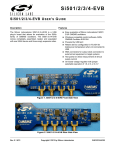
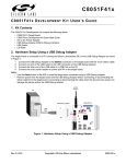
C P 2 11 4 - E K CP211 4 E VALUATION K I T U SER ’ S G UIDE 1. Kit Contents The CP2114 Evaluation Kit is available in four configurations shown in Table 1: Table 1. Evaluation Kits Kit Name Components CP2114 CP2114-EK evaluation board cable RS-232 serial cable CP2114 evaluation board Daughter card with Cirrus Logic CS42L55 CODEC Ear bud headphones Audio cable (3.5 mm male to male) USB Cable RS-232 serial cable CP2114 evaluation board Daughter card with Wolfson Microelectronics WM8523 DAC Ear bud headphones USB Cable RS-232 serial cable CP2114 evaluation board Daughter card with Texas Instruments PCM1774 DAC Ear bud headphones USB Cable RS-232 serial cable USB CP2114-CS42L55EK CP2114-WM8523EK CP2114-PCM1774EK This document applies to all CP2114 kits. 2. Software Setup The example applications as well as additional documentation can be found here: www.silabs.com/CP2114 AN721 Software (AN721SW) USB and GPIO configuration utility: See AN721 for more information on customizing USB and GPIO settings. (DAC/CODEC) configuration utility: See Section 4 for more information using the DAC Configuration utility. Audio CP2114 Data Sheet CP2114 Evaluation Kit User's Guide AN433: CP2110/4 HID-to-UART API Specification AN434: CP2110/4 Interface Specification CP2114 Quick Start Guide Rev. 0.1 10/12 Copyright © 2012 by Silicon Laboratories CP2114-EK CP2114-EK 3. CP2114 Hardware Interface For information on using the CP2114, see the CP2114 Quick Start Guide, available at www.silabs.com/CP2114. Figure 1, Figure 2, Figure 3, and Figure 4 show each evaluation board as well as important features. RS-232 Connector DAC Select Jumpers USB Active and Suspend LEDs Microphone Input Path Daughter Card Connector USB Connector TX and RX Toggle LEDs Volume Control Buttons Figure 1. CP2114 Evaluation Board Features 2 Rev. 0.1 CP2114-EK Line Out Connector Headphone Out Connector Daughter Card Connector CS42L55 Codec Analog Input Connector Figure 2. CS42L55 Daughter Card Features Line Out Connector Headphone Out Connector Daughter Card Connector WM8523 DAC Figure 3. WM8523 Daughter Card Features Rev. 0.1 3 CP2114-EK Analog Input Connector Headphone/ Line Out Connector Daughter Card Connector PCM1774 DAC Figure 4. PCM1774 Daughter Card Features 4 Rev. 0.1 CP2114-EK 4. DAC Configuration Application (AN721SW) The DAC Configuration utility is an application within the AN721 software (AN721SW) package that allows audio configuration strings to be sent to the CP2114 one-time programmable memory or RAM. The audio string is used by the CP2114 to configure the DAC/CODEC. To access the DAC Configuration utility, run the AN721SW and connect to the CP2114 device. After connecting to the device, select Advanced Configuration, then DAC Configuration. After this, the DAC Configuration utility shown in Figure 5 will appear. This AN721SW package is available at www.silabs.com/CP2114. Figure 5. AN721: DAC Configuration 4.1. Application Command Descriptions 4.1.1. Get CP2114 Capabilities This button will report the current configuration of the one-time programmable memory. With the default pin configuration and no jumpers installed on GPIO.5, GPIO.6, GPIO.7, or GPIO.8, the utility will display the following: * CP2114 Caps AvailableBootIndices: 0x20 AvailableOtpConfigs: 0x1D CurrentBootConfig: 0xFF AvailableOtpConfigSpace: 0x1532 The AvailableBootIndices: 0x20 parameter indicates that all 32 boot index slots are available for programming. The AvailableOtpConfigs: 0x1D parameter indicates that there are 29 CP2114 configurations available in the one-time programmable memory. Rev. 0.1 5 CP2114-EK The CP2114 EVB ships with three default configurations in OTP at the following indices: Index 0: Audio out and audio in streams both set to Asynchronous with CS42L55 DAC settings. Index 1: Audio out and audio in streams both set to Asynchronous with WM8523 DAC settings. Index 2: Audio out and audio in streams both set to Asynchronous with PCM1774 DAC settings. The CurrentBootConfig parameter with a value of 0xFF indicates the CP2114 will not configure any DAC devices on a reset or boot.This occurs when DAC select input feature is turned on and no jumpers are installed on GPIO.5, GPIO.6, GPIO.7, and GPIO.8. DAC select input feature is turned on and the GPIO value is set to “Use OTP Boot Config” while no valid boot config entry is found in the one-time programmable memory. DAC select input feature is turned off and there is no valid Boot Config entry in the one-time programmable memory. The CP2114 has 32 programmable boot configuration entries by default. (The CP2114 boot configuration can be changed up to a total of 32 times.) The final parameter, AvailableOtPConfigSpace: 0x1532 indicates there are 0x1532 (5426) bytes of programmable memory available to support new configurations. 4.1.2. Reset Device This button forces a CP2114 reset. 4.1.3. Load Config Text from File Loads configuration text from a file into the Config Text window. 4.1.4. Save Config Text to File Saves the text in the Config Text window to a file. 4.1.5. Write Config Text to RAM Writes the configuration displayed in the Config Text window into the CP2114 RAM. The DAC configurations are also written to the DAC. This operation will cause the CP2114 to disconnect and reconnect on the USB bus. This configuration is not retained on device reset. 4.1.6. Write Config Text to OTP Writes the configuration in the Config Text window to the one-time programmable memory. The configuration does not become the active configuration in RAM unless it’s specified in CP2114 Boot Config or via DAC select GPIO pins followed by power cycling or resetting the device. 4.1.7. Read CP2114 Config from OTP After specifying the configuration number in the text box to the right of the button and clicking the button, the utility will display the one-time programmable memory configuration in the output window. 4.1.8. Set CP2114 Boot Config After specifying the configuration number in the text box to the right of the button and clicking the button, the boot configuration index is programmed into the one-time programmable memory space. Note: The CP2114 boot configuration index can be changed up to 32 times. 4.1.9. Get DAC Registers Displays one or more DAC registers in the output window. To display a contiguous range of DAC registers enter the starting register address in the Start Address field and the number of registers to read in the Num Registers field. Click Get DAC Registers and the register values will be displayed in the status window as hex comma-separated values. 4.1.10. Save Final Device Customization to File Save the final 5.5 kB of customized data into a file for one-time programming in production. 6 Rev. 0.1 CP2114-EK 4.2. Using the Application Use the following steps to program the CP2114 using the DAC configuration utility: 1. Click Get CP2114 Capabilities and note the boot index, available OTP boot index slots, and available OTP config space. 2. Click Load Config Text from File if there is one available; otherwise write the config text into the Config Text window directly. 3. Click Write Config Text to RAM. This will cause CP2114 to re-enumerate over USB. Once CP2114 device is seen by the Host again, verify the device's audio functionalities including volume control and mute control. Adjust the value in Config Text if necessary and repeat Write Config Text to RAM until desired result is achieved. 4. Verify the DAC registers have the desired setting by entering the Start Address and Num Registers and clicking Get DAC Registers. 5. Click Save Config Text to File to save a copy of the text in the Config Text window. 6. Click Write Config Text to OTP after all functionalities have been completely verified in RAM. The new config will consume one Boot Config index slot and some one-time programmable config space. The index of this new config should be the next available index. For example, if Get CP2114 Capabilities returned AvailableOtpConfigs of 0x1D, this Configuration index will be 3. 7. Enter the index of the new config and click Read CP2114 Config from OTP. Verify the data returned is as expected. 8. Click Get CP2114 Capabilities and verify the available OTP config space is (2+Config Data bytes) less than the previous value. The firmware inserts 2-byte length before the Config Data when writing to OTP. Available OTP Configs should be 1 less than the previous value. 9. Enter the Configuration index of the new Config and click Set CP2114 Boot Config to make CP2114 to boot from the new Config. 10. Reset the CP2114. 11. Verify CP2114 boots up properly with DAC functioning properly. Verify volume and mute integration with the Host. Click Save Final Device Configuration to File for OTP programming in production. 4.3. Audio Configuration String Format The audio configuration string input format is comma or space-separated hex values (a combination of comma and space separation is not allowed).The CP2114 data sheet available at www.silabs.com/CP2114 discusses the audio configuration string in detail. Rev. 0.1 7 CP2114-EK 5. Evaluation Board Overview 5.1. CP2114-EB Overview The CP2114 Evaluation Kit includes an evaluation board with a CP2114 device pre-installed for user evaluation and software development. Numerous input/output (I/O) connections are provided to facilitate prototyping using the evaluation board. Refer to Figure 6 for the locations of the various I/O connectors. J1 J2 J3 JP00-JP30 JP40 JP41 JP42 JP43 JP44 JP45 JP46 JP47 JP48 JP49 JP50, JP52 D2 D3 D4 D5 D6 SW1-SW4 SW5 8 Daughter card connector USB connector for USB interface DB9 connector for RS-232 interface CP2114 pin connector VIO power connector REGIN Power Connector and Self-Powered Mode Connector Test point connector Si500 enable connector SCKIN to SCK connector DAC selection connector Green USB ACTIVE LED connector Red USB SUSPEND LED connector Daughter card reset connector CP2114 GPIO signal header Daughter card GPIO signal header Red record mute LED Red receive toggle LED Red transmit toggle LED Red USB SUSPEND LED Green USB ACTIVE LED Audio control buttons Reset button Rev. 0.1 CP2114-EK J3 DAC Select RESET SILICON LABS JP41 JP42 JP40 CP2114 U1 Si500 www.silabs.com PB MUTE REC MUTE VOL S3 J2 U3 D2 CP2114-EB S5 S4 S1 JP43 TXT D4 D3 RXT JP52 JP48 JP17 JP16 JP15 JP14 JP13 JP12 JP11 JP10 JP07 JP06 JP05 JP04 JP03 JP02 JP01 JP00 JP44 J1 JP20 JP21 JP50 JP49 JP45 SUSPEND D5 JP46 JP47 JP22 JP23 JP24 JP25 JP26 JP30 ACTIVE D6 VOL + S2 Figure 6. CP2114 Evaluation Board with Default Shorting Blocks Installed 5.1.1. Daughter Card Connector (J1) The J1 connector is used to connect to a CP2114 daughter card. 5.1.2. Universal Serial Bus (USB) Interface (J2) A Universal Serial Bus (USB) connector (J2) is provided to facilitate connections to the USB interface on the CP2114. See Table 2 for the USB pin definitions. Table 2. USB Connector Pin Descriptions Pin # Description 1 2 3 4 VBUS D– D+ GND (Ground) Rev. 0.1 9 CP2114-EK 5.1.3. UART Signals (J3) An RS-232 transceiver circuit and DB9 connector (J3) are provided on the evaluation board to connect the CP2114 to external serial devices. See Table 3 for the RS-232 J3 pin descriptions. Table 3. RS-232 Pin Descriptions Pin Signal 2 3 5 7 8 RXD TXD GND RTS CTS CP2114 Direction Input Output Output Input Description Receive Data Transmit Data Ground Request to Send Clear to Send 5.1.4. CP2114 Pin Connectors (JP00-JP30) The JP00-JP30 connectors connect and disconnect CP2114 pins from external circuits. By default, all of these jumpers are populated. 5.1.5. VIO Power Connector (JP40) This header (JP40) is included on the evaluation board to provide VIO power options. Populating the shorting block connects the CP2114 VIO input (pin 6) to CP2114 VDD (pin 7). Remove the shorting block to power VIO from an external source and connect the power source to pin 2 of the header. 5.1.6. REGIN Power Connector and Self-Powered Mode Connector (JP41) The JP41 header is used to connect the CP2114 REGIN pin (pin 8) to the VBUS source from the USB connector (default) or to the CP2114 VDD pin (pin 7). When connected to the VBUS source, the device is intended for buspowered operation. When connected to the CP2114 VDD pin, the device is intended for self-powered operation. In self-powered operation, an external power source can be connected to the JP41 header to power the VDD pin directly. 5.1.7. Test Point Connector (JP42) The JP42 header contains test points and is not used in normal operation. 5.1.8. Si500 Enable Connector (JP43) The JP43 header controls the power to the Si500 CMOS clock. Shorting pin 1 to pin 2 on the header will connect CP2114 VDD (pin 7) to the Si500. Shorting pin 2 to pin 3 on the header will place the Si500 in powerdown mode. The setting of JP43 depends on the desired clocking mode. 5.1.9. SCK to SCKIN Connector (JP44) The JP44 jumper should be left installed. 5.1.10. DAC Selection Connector (JP45) The JP45 header is used to select the CP2114 boot configuration after a reset. When a jumper is populated, the corresponding GPIO pin in connected to ground. When a jumper is removed, the corresponding GPIO pin is weakly pulled high. Note: If any of the four DAC select pins are configured for a function other than DAC selection, the CP2114 will not use the DAC select pins to choose a boot configuration. 5.1.11. Green USB ACTIVE LED and Connector (JP46, D6) The JP46 header is used to connect the CP2114 SUSPEND pin (pin 18) to the D6 green LED. When the LED is on, the device has enumerated with the PC operating normally. When the LED is off, the device has not yet enumerated or is in the USB Suspend state. 5.1.12. .Red USB SUSPEND LED and Connector (JP47, D5) 10 Rev. 0.1 CP2114-EK The JP47 header is used to connect the CP2114 SUSPEND pin (pin 17) to the D5 red LED. When the LED is on, the device has enumerated with the PC operating normally. When the LED is off, the device has not yet enumerated or is in the USB Suspend state. 5.1.13. Daughter Card Reset Connector (JP48) The JP48 header connects reset to the GPIO4_C pin on the daughter card connector (J1). On the CS42L55 daughter card, GPIO4_C is connected to the CS42L55 RESET pin. The GPIO4_C pin is unconnected on the WM8523 and PCM1774 daughter cards because the DACs do not have a hardware reset input. 5.1.14. CP2114 GPIO Signal Connector (JP49) The connector JP49 provides easy access to all of the CP2114 GPIO signals. 5.1.15. Daughter Card Signal Header (JP50, JP52) The headers JP50 and JP52 allow the connection of GPIO0-4 signals to the corresponding daughter card signals (GPIOx_C). These jumpers can be used to route the appropriate GPIO signals to a custom daughter card. 5.1.16. Audio Control Buttons and Red Record Mute LED (SW1-SW4, D2) SW1 through SW4 send audio control commands when pressed. In addition, the red record mute LED (D2) will turn on when the record mute button is pressed (SW4). Table 4. Audio Control Buttons LED Pins S1 Volume – S2 Volume + S3 Playback Mute S4 Record Mute 5.1.17. Red Receive Toggle and Transmit Toggle LEDs (D3, D4) The LEDs D3 and D4 will toggle when transmitting and receiving UART data. In order to use this functionality, the GPIO pins must first be configured for TX Toggle and RX Toggle modes. By default, these pins are used for DAC select 0 and DAC select 1. 5.1.18. Reset Button (SW5) SW5 externally pulls the CP2114 reset pin (pin 10) low when pressed. If SW5 is held down, the CP2114 will remain in reset until the button is released. Rev. 0.1 11 CP2114-EK 5.2. CS42L55-EB Overview The CS42L55 evaluation board contains a pre-installed CS42L55 for evaluation and preliminary software development with the CP2114 evaluation board. Refer to Figure 7 for the locations of the various I/O connectors on the CS42L55-EB. P1 P2 P3 P4 J1-J5 J9, J10 Daughter card connector Analog input connector Line output connector Headphone output connector I2S/I2C signal connectors I2S/I2C signal connectors LINE OUT P3 J1 HP OUT J2 P4 J4 P1 J3 J10 J5 CS42L55 J9 U1 AIN P2 SILICON LABS CP2114-CS42L55-EVB www.silabs.com Figure 7. CS42L55 Evaluation Board with Default Shorting Blocks Installed 5.2.1. Daughter Card Connector (P1) The P1 connector is used to connect to a CP2114 evaluation board (CP2114-EB). The CS42L55-EB must be plugged into a CP2114 evaluation board to function properly. 5.2.2. Analog Input Connector (P2) The P2 connector is used to connect an input device to the CS42L55 evaluation board. 5.2.3. Line Output Connector (P3) The P3 connector is used to connect powered speakers to the CS42L55 evaluation board. 5.2.4. Headphone Output Connector (P4) The P4 connector is used to connect headphones to the CS42L55 evaluation board. 5.2.5. I2S/I2C Signal Connectors (JP1-JP5, JP9, JP10) Connectors JP1 through JP7, JP9, and JP10 are provided to allow access to the I2S/I2C signals between the CP2114 and CS42L55. Placing a shorting block between pins 1 and 2 will connect the CP2114 to the CS42L55. Placing a shorting block between pins 2 and 3 will connect the corresponding CS42L55 pin to ground. When monitoring the I2S signals, connect the scope probe ground lead to the adjacent ground pin. 12 Rev. 0.1 CP2114-EK 5.3. WM8523-EB Overview The WM8523 evaluation board contains a pre-installed WM8523 for evaluation and preliminary software development with the CP2114 evaluation board. Refer to Figure 8 for the locations of the various I/O connectors on the WM8523-EB. J1 J2 J3 JP2-JP10 JP11 JP12 JP13 JP14 JP15 JP16-JP20 Daughter card connector Line output connector Headphone output connector I2S and I2C signal connectors Voltage regulator input connector WM8253 supply voltage header WM8253 supply voltage connector Headphone amplifier SHDN header Ground header GPIO header for SHDN control HP OUT J3 JP15 JP12 JP13 JP9 JP10 LINE OUT JP14 JP11 J2 JP19 JP20 JP16 JP17 JP18 J1 JP7 JP8 WM8523 JP5 U1 JP6 JP3 JP4 SILICON LABS JP2 CP2114-WM8523-EVB www.silabs.com Figure 8. WM8253 Evaluation Board with Default Shorting Blocks Installed 5.3.1. Daughter Card Connector (J1) The J1 connector is used to connect to a CP2114 evaluation board (CP2114-EB). The WM8253-EB must be plugged into a CP2114 evaluation board to function properly. 5.3.2. Line Output Connector (J2) The J2 connector is used to connect powered speakers to the WM8253 evaluation board. 5.3.3. Headphone Output Connector (J3) The J3 connector is used to connect headphones to the WM8253 evaluation board. 5.3.4. I2S/I2C Signal Connectors (JP2-JP10) Connectors JP2 through JP10 are provided to allow access to the I2S/I2C signals between the CP2114 and WM8253. Placing a shorting block between pins 1 and 2 will connect the CP2114 to the WM8253. Placing a shorting block between pins 2 and 3 will connect the corresponding WM8253 pin to ground. When monitoring the I2S signals, connect the scope probe ground lead to the adjacent ground pin. Rev. 0.1 13 CP2114-EK 5.3.5. Voltage Regulator Connector (JP11) The JP11 connector is used to connect the VBUS signal being supplied to the CP2114 to the input of the voltage regulator on the WM8253 evaluation board. Installing this jumper connects the VBUS signal to the regulator output. If another voltage supply is used, JP11 should be removed and the supply should be connected to pin 2 of the header. 5.3.6. WM8253 Supply Voltage Header (JP12) The JP12 header provides access to the WM8253 supply voltage. 5.3.7. WM8253 Supply Voltage Connector (JP13) This header (JP13) is included on the evaluation board to provide several power options for the WM8253. The following describes the function of each pin: Shorting pins 1,2: Connects the regulator output on the WM8253-EB to the supply of the WM8253. Shorting pins 2,3: Connects the CP2114 VDD (CP2114 pin 7) to the supply of the WM8253. 5.3.8. Headphone Amplifier SHDN Header (JP14, JP16–JP20) The jumpers JP14 and JP16-JP20 control the headphone amplifier shutdown (SHDN) pin. The headphone amplifier is enabled when SHDN is high and disabled when SHDN is low. In the default configuration (jumper shorting pins1 and 2), the headphone amp is always enabled. Shorting pins 2 and 3 on JP14 will disable the headphone amplifier. Removing JP14 and connecting one of JP16-JP20 allows the host to control the headphone amp via GPIO pin. In this case, the corresponding GPIO-GPIO_C jumper must also be installed on the CP2114-EK board. 5.3.9. Ground Header (JP15) The JP15 header provides access to ground. 14 Rev. 0.1 CP2114-EK 5.4. PCM1774-EB Overview The PCM1774 evaluation board includes contains a pre-installed a PCM1774 for evaluation and preliminary software development with the CP2114 evaluation board. Refer to Figure 9 for the locations of the various I/O connectors on the PCM1774-EB. J1 J2 J3 JP1-JP7 JP8 JP9 JP15, JP16 Daughter card connector Headphone/line output connector Analog input connector I2S signal connectors Voltage regulator connector PCM1774 supply voltage connector External capacitor connectors ANALOG IN J3 HP/LINE OUT JP9 JP8 J2 J1 JP15 JP16 PCM1774 U1 JP6 JP7 JP4 JP5 JP2 JP3 JP1 SILICON LABS CP2114-PCM1774-EVB www.silabs.com Figure 9. PCM1774 Evaluation Board with Default Shorting Blocks Installed 5.4.1. Daughter Card Connector (J1) The J1 connector is used to connect to a CP2114 evaluation board (CP2114-EB). The PCM1774-EB must be plugged into a CP2114 evaluation board to function properly. 5.4.2. Headphone/Line Output Connector (J2) The J2 connector is used to connect headphones or powered speakers to the PCM1774 evaluation board. 5.4.3. Analog Input Connector (J3) The J3 connector is used to connect an input device to the PCM1774 evaluation board. 5.4.4. I2S/I2C Signal Connectors (JP1–JP7) Connectors JP1 through JP7 are provided to allow access to the I2S/I2C signals between the CP2114 and PCM1774. Placing a shorting block between pins 1 and 2 will connect the CP2114 to the PCM1774. Placing a shorting block between pins 2 and 3 will connect the corresponding PCM1774 pin to ground. When monitoring the I2S signals, connect the scope probe ground lead to the adjacent ground pin. 5.4.5. Voltage Regulator Connector (JP8) The JP8 connector is used to connect the VBUS signal being supplied to the CP2114 to the input of the voltage regulator on the PCM1774 evaluation board. Installing this jumper connects the VBUS signal to the regulator output. If another voltage supply is used, JP8 should be removed and the supply should be connected to pin 2 of the header. Rev. 0.1 15 CP2114-EK 5.4.6. PCM1774 Supply Voltage Connector (JP9) This header (JP9) is included on the evaluation board to provide several power options for the PCM1774. The following describes the function of each pin: Shorting pins 1,2: Connects the regulator output on the PCM1774-EB to the supply of the PCM1774. Shorting pins 2,3: Connects the CP2114 VDD (CP2114 pin 7) to the supply of the PCM1774. 5.4.7. External Capacitor Connectors (JP15, JP16) The JP15 and JP16 connectors allow external capacitors to be connected to the HP/LINE OUT connector. For best low frequency response (35 Hz cutoff), remove the jumpers on JP15 and JP16. For maximum power output (45 Hz cutoff), place the jumpers on JP15 and JP16. 16 Rev. 0.1 Figure 10. CP2114 Evaluation Board Schematic CP2114-EK 6. Schematics Rev. 0.1 17 Figure 11. CS42L55 Evaluation Board Schematic CP2114-EK 18 Rev. 0.1 Figure 12. WM8523 Evaluation Board Schematic CP2114-EK Rev. 0.1 19 Figure 13. PCM1774 Evaluation Board Schematic CP2114-EK 20 Rev. 0.1 CP2114-EK 7. Bill of Materials Table 5. CP2114 Evaluation Board (CP2114-EB) Bill of Materials Reference Part Number Source Description C18 C0603X5R6R3-475K Venkel 4.7 µF 6.3 V ±10% X5R 0603 C19 C20 C21 C22 C0603X7R250-104K Venkel 0.1 µF 25 V ±10% X7R 0603 C6 C8 C13 C23 C25 C0603X5R160-105K Venkel 1 µF 16 V ±10% X5R 0603 C7 C9 C10 C11 C12 C14 C15 C16 C17 C24 C26 C0402X7R160-104K Venkel 0.1 µF 16 V ±10% X7R 0402 D1 SP0503BAHTG Littlefuse 300 mW 20 V TVS SOT143-AKKK D2 D3 D4 D5 SML-LX0603IW Lumex Inc. RED 30 mA LED 0603 D6 SML-LX0603GW Lumex Inc. GREEN 25 mA LED 0603 J1 PCN10C-20S-2.54DS(72) Hirose Electric Co Ltd CONN, DIN HEADER, 20POS, DUAL R/A, FEMALE J2 292304-1 Tyco USB Type B Connector J3 D09P33E4GX00LF FCI DB9 MALE RA D-SUB J4 JP00 JP03 JP04 JP05 JP06 JP07 JP10 JP11 JP12 JP13 JP14 JP15 JP16 JP17 JP20 JP21 JP22 JP23 JP24 JP25 JP26 JP30 JP40 JP44 JP46 JP47 JP48 JP52 TSW-102-07-T-S Samtec JUMPER Header CONN1X2 JP01 JP02 JP41 JP42 JP43 JP50 TSW-103-07-T-S Samtec JUMPER Header CONN1X3 JP45 TSW-104-07-T-D Samtec JUMPER Header CONN4x2 JP49 TSW-112-07-T-S Samtec JUMPER Header CONN1x12 Rev. 0.1 21 CP2114-EK Table 5. CP2114 Evaluation Board (CP2114-EB) Bill of Materials Reference Part Number Source Description JS1 JS2 JS3 JS4 JS5 JS6 JS7 JS8 JS9 JS10 JS11 JS12 JS13 JS14 JS15 JS16 JS17 JS18 JS19 JS20 JS21 JS22 JS23 JS24 JS30 JS32 JS33 JS35 JS37 JS38 JS39 JS40 JS41 SNT-100-BK-T Samtec Jumper Shunt R1 R2 R3 R4 R9 CR0402-16W-471J Venkel 470 1/16 W ±5% ThickFilm 0402 R21 R22 R23 R24 R25 R26 R28 R30 R32 CR0603-10W-103J Venkel 10K 1/10 W ±5% ThickFilm 0603 R27 R29 R31 R33 CR0603-10W-472J Venkel 4.7K 1/10 W ±5% ThickFilm 0603 R34 R35 R36 R37 R38 R39 R40 R41 CR0201-20W-33R0F Venkel 33 1/20 W ±1% ThickFilm 0201 R5 R6 CR0603-16W-102J Venkel 1K 1/16 W ±5% ThickFilm 0603 R7 R8 CR0603-10W-1201F Venkel 1.20K 1/10 W ±1% ThickFilm 0603 S1 S2 S3 S4 S5 EVQ-PAD04M Panasonic Corp Momentary Tactile Switch SW4N6.5X4.5 TP11 TP12 TP13 TP14 TP15 TP16 TP17 TP18 TP19 TP20 TP21 TP22 151-207-RC Kobiconn RED Loop Testpoint U1 CP2114-B01-GM Silicon Laboratories CP2114 USB Audio to Digital Audio Bridge QFN32N5X5P0.5 U2 SP3223EUCY-L Exar Corporation RS232 Transceiver TSSOP20N6.4P0.65 U3 500SAAC48M0000ACF SiLabs 48 MHz 3.3 V CMOS ±150PPM Si500S OSC4N3.2X4.0 22 Rev. 0.1 CP2114-EK Table 6. Cirrus Logic CS42L55 Evaluation Board (CS42L55-EB) Bill of Materials Reference Part Number Source Description C8-10 C2829 C0603C104J3RACTU Kemet CAP, 0.1 µF, X7R, CERAMIC, 0603, 25 V, ±5%, OR EQ, RoHS. C15-16 C19 C33 C1608X7R1C105K TDK Corporation CAP CERAMIC, 1.0 µF, X7R, 0603, 16 V, ±10%, OR EQ, RoHS. C13-14 CC0805JRNPO9BN102 Yageo CAP CERAMIC, 1000 pF, NPO, 0805, 50 V, ±5%, OR EQ, RoHS. C2 EMK212BJ106KG-T Taiyo Yuden CAP, CER, 10µF, 16V, X5R, 0805 OR EQ, RoHS C20-21 ECJ-2VC1H152J Panasonic Electronic Components CAP, 1500 pF, NP0, CERAMIC, 0805, 50 V , ±5%, OR EQ, RoHS. C17-18 GRM2165C1H182JA01D Murata Electronics North America CAP, 1800 pF, NP0, CERAMIC, 0805, 50 V , ±5%, OR EQ, RoHS. C3-7 C11-12 GRM188R61C225KE15D Murata Electronics North America CAP, 2.2 µF , CERAMIC , 16 V , X5R, 0603, ±10% , OR EQ, RoHS. C1 EMK212BJ475KG-T Taiyo Yuden CAP, CER, 4.7 µF, 16 V, 10%, X5R, 0805 OR EQ, RoHS. P1 PCN10-20P-2.54DS(72) Hirose Electric Co Ltd CONN, DIN HEADER, 20POS, DUAL R/A, MALE, RoHS. U1 CS42L55-CNZ Cirrus Logic Inc STEREO CODEC,QFN36-5X5 mm , RoHS. J6 PBC02SAAN Sullins Connector Solutions STAKE HEADER, 1X2, 0.1"CTR, GOLD, OR EQ, RoHS. J1-5 J9-10 PBC03SAAN Sullins Connector Solutions STAKE HEADER, 1X3, 0.1" CTRS, OR EQ, RoHS. U2 LT1963AEST-2.5 Linear Technology LDO REG, 2.5 V, 1.5 A, SOT223 R10-11 ERJ-3EKF1000V Panasonic Electronic Components RES, 100 OHM, SMT, 0603, 1/10 W, ±1%, OR EQ, RoHS. R8-9 RT0805FRE0733R2L Yageo RES, 33.2 OHM, SMT, 0805, 1/8 W, ±1%, OR EQ, RoHS. R12-13 ERJ-6ENF5620V Panasonic Electronic Components RES, 562 OHM, SMT, 0805, 1/8 W, ±1%, OR EQ, RoHS. R1-5 N/A SH1-7 SPC02SYAN Sullins Connector Solutions CONN, JUMPER SHORTING, TIN, OR EQ, RoHS. SF1-4 SJ61A6 3M BUMPON PROTECTIVE, BUMPER , SILICONE, OR EQ, RoHS. P2-4 SJ1-3535NG CUI Inc CONN, JACK STEREO, 3 POS, 3.5 MM, PTH, RoHS. TP3 5002 Keystone Electronics TEST POINT, PC COMPACT, .063"D WHITE, OR EQ, RoHS. SOLDER BUMP JUMPER, NC, 0402 Components Not Installed (NI) R6-7 RES, SMT, 0603, OR EQ, RoHS. (NI) Rev. 0.1 23 CP2114-EK Table 7. Wolfson Microelectronics WM8523 Evaluation Board (WM8523-EB) Bill of Materials Reference Part Number Source Description C1 C2 C15 C16 C0805X5R160-475K Venkel 4.7 µF 16 V ±10% X5R 0805 C19 C20 C1206X7R250-105K Venkel 1 µF 25 V ±10% X7R 1206 C4 C7 C12 C13 C14 C0805X7R160-105M Venkel 1 µF 16 V ±20% X7R 0805 C6 C0603X7R100-225K Venkel 2.2 µF 10 V ±10% X7R 0603 C8 C9 C1206C0G500-473J Venkel 47 nF 50 V ±5% COG 1206 J1 PCN10-20P-2.54DS(72) Hirose Electric Co Ltd CONN, DIN HEADER, 20POS, DUAL R/A, MALE, RoHS. J2 J3 SJ1-3535NG CUI Audio Jack JP11 JP12 JP15 JP16 JP17 JP18 JP19 JP20 TSW-102-07-T-S Samtec JUMPER Header CONN1X2 JP2 JP3 JP4 JP5 JP6 JP7 JP8 JP9 JP10 JP13 JP14 TSW-103-07-T-S Samtec JUMPER Header CONN1X3 JS1 JS2 JS3 JS4 JS5 JS6 JS7 JS8 JS9 JS10 JS11 SNT-100-BK-T Samtec Jumper Shunt R1 R2 R5 R6 R7 R10 R11 CR0603-10W-1002F Venkel 10K 1/10 W ±1% ThickFilm 0603 R8 R9 CR0603-10W-1270F Venkel 127 1/10 W ±1% ThickFilm 0603 SF1 SF2 SF3 SF4 SJ61A6 3M BUMPON PROTECTIVE, BUMPER , SILICONE, OR EQ, RoHS. U1 WM8523GEDT Wolfson Microelectronics WM8523GEDT DAC TSSOP20N6.4P0.65 U2 LT1963AEST-3.3#PBF Linear Technologies 3.3 V 1.5 A max LDO SOT223 U3 MAX9722AETE Maxim 130 mW 2.4 V-5.5 V AMPLIFIER QFN16N3X3P0.5E 24 Rev. 0.1 CP2114-EK Table 8. Texas Instruments PCM1774 Evaluation Board (PCM1774-EB) Bill of Materials Reference Part Number Source Description C1 C2 C15 C16 C19 C20 C21 C0805X5R160-475K Venkel 4.7 µF 16 V ±10% X5R 0805 C10 C11 TA016TCM106KA Venkel 10 µF 16 V ±10% TANT C3216 C17 C18 ECA1CM221 Panasonic 220 µF 16 V ±20% Alum_Elec C2.5X6.3 MM C22 C23 C24 C25 C0603X7R250-104K Venkel 0.1 µF 25 V ±10% X7R 0603 J1 PCN10-20P-2.54DS(72) Hirose Electric Co Ltd CONN, DIN HEADER, 20POS, DUAL R/A, MALE, RoHS. J2 J3 SJ1-3535NG CUI Audio Jack JP1 JP2 JP3 JP4 JP5 JP6 JP7 JP9 TSW-103-07-T-S Samtec JUMPER Header CONN1X3 JP8 JP15 JP16 TSW-102-07-T-S Samtec JUMPER Header CONN1X2 JS1 JS3 JS4 JS6 JS7 JS9 JS10 JS11 JS12 SNT-100-BK-T Samtec Jumper Shunt R10 R11 R12 R13 R14 R15 CR0603-16W-22R0F Venkel 22 1/16 W ±1% ThickFilm 0603 R3 CR0603-10W-1002F Venkel 10K 1/10 W ±1% ThickFilm 0603 R8 R9 CR0805-10W-4R7J Venkel 4.7 1/10 W ±5% ThickFilm 0805 SF1 SF2 SF3 SF4 SJ61A6 3M BUMPON PROTECTIVE, BUMPER , SILICONE, OR EQ, RoHS. TP1 TP2 TP3 151-207-RC Kobiconn RED Loop Testpoint U1 PCM1774RGP Texas Instruments PCM1774 DAC QFN20N4X4P0.5 U2 LT1963AEST-3.3#PBF Linear Technologies 3.3 V 1.5 A max LDO SOT223 Rev. 0.1 25 CP2114-EK CONTACT INFORMATION Silicon Laboratories Inc. 400 West Cesar Chavez Austin, TX 78701 Tel: 1+(512) 416-8500 Fax: 1+(512) 416-9669 Toll Free: 1+(877) 444-3032 Please visit the Silicon Labs Technical Support web page: https://www.silabs.com/support/pages/contacttechnicalsupport.aspx and register to submit a technical support request. Patent Notice Silicon Labs invests in research and development to help our customers differentiate in the market with innovative low-power, small size, analogintensive mixed-signal solutions. Silicon Labs' extensive patent portfolio is a testament to our unique approach and world-class engineering team. The information in this document is believed to be accurate in all respects at the time of publication but is subject to change without notice. Silicon Laboratories assumes no responsibility for errors and omissions, and disclaims responsibility for any consequences resulting from the use of information included herein. Additionally, Silicon Laboratories assumes no responsibility for the functioning of undescribed features or parameters. Silicon Laboratories reserves the right to make changes without further notice. Silicon Laboratories makes no warranty, representation or guarantee regarding the suitability of its products for any particular purpose, nor does Silicon Laboratories assume any liability arising out of the application or use of any product or circuit, and specifically disclaims any and all liability, including without limitation consequential or incidental damages. Silicon Laboratories products are not designed, intended, or authorized for use in applications intended to support or sustain life, or for any other application in which the failure of the Silicon Laboratories product could create a situation where personal injury or death may occur. Should Buyer purchase or use Silicon Laboratories products for any such unintended or unauthorized application, Buyer shall indemnify and hold Silicon Laboratories harmless against all claims and damages. Silicon Laboratories and Silicon Labs are trademarks of Silicon Laboratories Inc. Other products or brandnames mentioned herein are trademarks or registered trademarks of their respective holders. 26 Rev. 0.1