
1
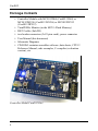
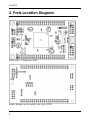
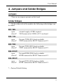
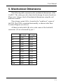
CardS12
HardwareVersion 1.00
User Manual
April 11 2005
CardS12
Copyright (C)2003-2005 by
ELMICRO Computer GmbH & Co. KG
Hohe Str. 9-13 D-04107 Leipzig, Germany
Tel.: +49-(0)341-9104810
Fax: +49-(0)341-9104818
Email: [email protected]
Web: http://elmicro.com
This manual and the product described herein were designed
carefully by the manufacturer. We have made every effort to avoid
mistakes but we cannot guarantee that it is 100% free of errors.
The manufacturer's entire liability and your exclusive remedy shall
be, at the manufacturer's option, return of the price paid or repair or
replacement of the product. The manufacturer disclaims all other
warranties, either expressed or implied, including but not limited to
implied warranties of merchantability and fitness for a particular purpose, with respect to the product including accompanying written material,
hardware, and firmware.
In no event shall the manufacturer or its supplier be liable for any
damages whatsoever (including, without limitation, damages for loss of
business profits, business interruption, loss of business information, or
other pecuniary loss) arising out of the use of or inability to use the
product, even if the manufacturer has been advised of the possibility of
such damages. The product is not designed, intended or authorized for
use in applications in which the failure of the product could create a
situation where personal injury or death may occur. Should you use the
product for any such unintended or unauthorized application, you shall
indemnify and hold the manufacturer and its suppliers harmless against
all claims, even if such claim alleges that the manufacturer was negligent regarding the design or implementation of the product.
Product features and prices may change without notice.
All trademarks are property of their respective holders.
User Manual
Contents
1. Overview . . . . . . . . . . . . . . . . . . . . . . . . . . . . . . . . . . . . . . . . . . . 3
...................................... 4
Package Contents . . . . . . . . . . . . . . . . . . . . . . . . . . . . . . . . . . . . 6
Technical Data
2. Quick Start . . . . . . . . . . . . . . . . . . . . . . . . . . . . . . . . . . . . . . . . . 7
3. Parts Location Diagram . . . . . . . . . . . . . . . . . . . . . . . . . . . . . 8
4. Jumpers and Solder Bridges . . . . . . . . . . . . . . . . . . . . . . . . . 9
........................................... 9
Solder Bridges . . . . . . . . . . . . . . . . . . . . . . . . . . . . . . . . . . . . . . . 9
Jumpers
5. Mechanical Dimensions . . . . . . . . . . . . . . . . . . . . . . . . . . . . 11
6. Circuit Description . . . . . . . . . . . . . . . . . . . . . . . . . . . . . . . . . 12
Schematic Diagram . . . . . . . . . . . . . . . . . . . . . . . . . . . . . . . . . . 12
Controller Core, Power Supply . . . . . . . . . . . . . . . . . . . . . . . . . 12
Reset Generation . . . . . . . . . . . . . . . . . . . . . . . . . . . . . . . . . . . 13
Clock Generation and PLL . . . . . . . . . . . . . . . . . . . . . . . . . . . . 14
Operating Modes, BDM Support . . . . . . . . . . . . . . . . . . . . . . . . 16
Integrated A/D-Converter . . . . . . . . . . . . . . . . . . . . . . . . . . . . . 16
Integrated EEPROM . . . . . . . . . . . . . . . . . . . . . . . . . . . . . . . . . 18
......................................
RS232 Interfaces . . . . . . . . . . . . . . . . . . . . . . . . . . . . . . . . . . .
SPI Bus . . . . . . . . . . . . . . . . . . . . . . . . . . . . . . . . . . . . . . . . . . .
IIC Bus . . . . . . . . . . . . . . . . . . . . . . . . . . . . . . . . . . . . . . . . . . .
CAN Interface . . . . . . . . . . . . . . . . . . . . . . . . . . . . . . . . . . . . . .
Indicator LED
20
20
22
23
25
7. Application Hints . . . . . . . . . . . . . . . . . . . . . . . . . . . . . . . . . . . 27
Behaviour after Reset . . . . . . . . . . . . . . . . . . . . . . . . . . . . . . . . 27
Startup Code . . . . . . . . . . . . . . . . . . . . . . . . . . . . . . . . . . . . . . . 27
Additional Information on the Web . . . . . . . . . . . . . . . . . . . . . . 27
1
CardS12
8. TwinPEEKs Monitor . . . . . . . . . . . . . . . . . . . . . . . . . . . . . . . . 28
Serial Communication . . . . . . . . . . . . . . . . . . . . . . . . . . . . . . . . 28
Autostart Function . . . . . . . . . . . . . . . . . . . . . . . . . . . . . . . . . . . 28
Write Access to Flash and EEPROM . . . . . . . . . . . . . . . . . . . . 28
Redirected Interrupt Vectors . . . . . . . . . . . . . . . . . . . . . . . . . . . 29
Usage . . . . . . . . . . . . . . . . . . . . . . . . . . . . . . . . . . . . . . . . . . . . 31
Monitor Commands . . . . . . . . . . . . . . . . . . . . . . . . . . . . . . . . . . 31
9. Memory Map . . . . . . . . . . . . . . . . . . . . . . . . . . . . . . . . . . . . . . 35
2
User Manual
1. Overview
CardS12 is an easy applicable, credit card-sized Controller Module,
based on the 16-bit microcontroller family HCS12 by Freescale
(formerly Motorola). The CardS12 module provides an easy way to
evaluate the microcontroller unit. It is a versatile tool for rapid prototyping and a very cost-effective, off-the-shelf solution for low- and
mid-volume series applications.
The CardS12 is equipped with a MC9S12D64 microcontroller unit
(MCU). It contains a 16-bit HCS12 CPU, 64KB of Flash memory, 4KB
RAM, 1KB EEPROM and a large amount of peripheral function blocks,
such as SCI, SPI, CAN, IIC, Timer, PWM, ADC and
General-Purpose-I/Os. The MC9S12D64 has full 16-bit data paths
throughout. An integrated PLL-circuit allows adjusting performance
vs. current consumption according to the needs of the user application.
There are two more versions of CardS12 available:
CardS12.DG256 is equipped with a MC9S12DG256 microcontroller
and CardS12.DP512 uses a MC9S12DP512.
For HCS12 microcontrollers, a wide range of software tools
(monitors, C-compilers, BDM-debuggers) is available to accelerate the
development process.
3
CardS12
Technical Data
w MCU MC9S12D64 with LQFP112 package (SMD)
w HCS12 16-bit CPU, uses same programming model and
command set as the HC12
w 16 MHz crystal clock, up to 25 MHz bus clock using PLL
w 64KB Flash
w 1KB EEPROM
w 4KB RAM
w 2x SCI - asynch. serial interface (e.g. RS232, LIN)
w 1x SPI - synch. serial interface
w 1x IIC - Inter-IC-Bus
w 1x msCAN-Module (CAN 2.0A/B-compatible), one channel
equipped with on-board high-speed physical interface driver
w 8x 16-Bit Timer (Input Capture/Output Compare)
w 8x PWM (Pulse Width Modulator)
w 16-channel 10-bit A/D-Converter
w BDM - Background Debug Mode Interface, std 6-pin connector
w Special LVI-circuit (reset controller)
w two serial interfaces with RS232 transceiver (e.g. for PC
connection)
w 2nd serial port can directly drive a serial LC display unit
w Indicator-LED
w Reset Button
w up to 87 free general-purpose I/Os
w all I/O-signals signals brought out on header connectors
w 5V operating voltage, current consumption 50 mA typ.
w Mech. Dimensions: 2.1" x 3.4"
4
User Manual
Extended Features of CardS12.DG256:
w
w
w
w
w
w
MCU MC9S12DG256
256KB Flash
4KB EEPROM
12KB RAM
3x SPI
additional msCAN module (busdriver circuit not included)
Extended Features of CardS12.DP512:
w
w
w
w
w
w
MCU MC9S12DP512
512KB Flash
4KB EEPROM
14KB RAM
3x SPI
four additional msCAN modules (no drivers on-board)
5
CardS12
Package Contents
w Controller Module with MC9S12D64 (CardS12.D64) or
MC9S12DG256 (CardS12.DG256) or MC9S12DP512
(CardS12.DP512)
w TwinPEEKs Monitor (in the MCU's Flash Memory)
w RS232 cable (Sub-D9)
w two header connectors (2x25 pins each), power connector
w User Manual (this document)
w Schematic Diagrams
w CD-ROM: contains assembler software, data sheets, CPU12
Reference Manual, code examples, C-compiler (evaluation
version), etc.
Controller Modul CardS12.D64
6
User Manual
2. Quick Start
Nobody likes to read big manuals. For that reason we will summarize the most important things in the following section. If you need
additional information, please refer to the more detailed sections of this
manual.
Here is how you can start:
w Please check the board for any damages due to transportation
w Connect the Controller Module via RS232 to a PC. The connection between CardS12 (interface SER0, connector X3) and PC
is simply made using the flat ribbon cable which is in the box.
w On the PC, start a Terminal Program. An easy to use Terminal
Program is OC-Console, which is available at no charge from
our Website!
w Select a baudrate of 19200 Bd. Disable all hardware or software
protocols.
w Connect a stabilized (!) power supply, e.g. here:
w GND to X7 pin 2
w +5V to X7 pin 1
w Check voltage and polarity before making the connection!
w Once powered up, the Monitor program will start, display a
message and await your commands.
We hope you will enjoy working with CardS12!
7
CardS12
3. Parts Location Diagram
Place Plan - Component Side
Solder Bridges on the solder side of the PCB
8
User Manual
4. Jumpers and Solder Bridges
Jumpers
There are no jumpers present on this board.
Solder Bridges
On the solder side of the module, the following solder bridges can
be found:
BR1: VRH
open
closed*
external supply of VRH required
VRH connected to VDDA (VCC) on-board
BR2: T1IN
open
closed*
Port pin TXD0 (PS1) freely available
TXD0 connected to RS232 Transceiver IC3
BR3: T2IN
open
closed*
Port pin TXD1 (PS3) freely available
TXD1 connected to RS232 Transceiver IC3
BR4: R1OUT
open
closed*
Port pin RXD0 (PS0) freely available
RXD0 connected to RS232 Transceiver IC3
BR5: R2OUT
open
closed*
Port pin RXD1 (PS2) freely available
RXD1 connected to RS232 Transceiver IC3
* = Factory Default Setting
9
CardS12
BR6, BR7: RS232 TxD/RxD Select (SER1)
1-2*
RS232 configured as "device"
(connection to a PC, etc.)
2-3
RS232 configured as "host"
(connection to a serial LCD, etc.)
BR8: LCD Power Supply (SER1)
open*
VCC not available on RS232 port SER1
(standard Sub-D connector layout)
closed
VCC available on RS232 port SER1
(at Pin 9 of the Sub-D connector)
BR9: RXCAN0
open
Port pin RXCAN0 (PM0) freely available
closed*
RXCAN0 connected to CAN-Transceiver IC4
* = Factory Default Setting
10
User Manual
5. Mechanical Dimensions
The following table summarizes the mechanical dimensions of the
CardS12. The values provide a basis for the design of carrier boards etc.
Please note: Always check all mechanical dimensions using the real
hardware module!
The reference point (0,0) is located at the "south/west" corner of
the PCB. The PCB is orientated horizontally, as shown in the Parts
Location Diagram (see above).
All data for holes/drills (B) refer to the center of the hole/drill,
connectors (X) are referenced by pin 1.
X in inch
Y in inch
X1
0,150
1,575
X2
2,600
1,700
X3
3,150
0,675
X4
3,150
1,825
X5
0,400
1,900
X6
0,400
0,100
X7
2,775
0,725
X8
0,150
0,950
B1
0,150
0,150
B2
0,150
1,950
B3
3,250
1,050
PCB
3,400
2,100
11
CardS12
6. Circuit Description
In this section, a number of details will be presented on how to
work with the HCS12 in general and the CardS12 Controller Module in
particular.
Please be aware that, even if this manual can provide some specific
hints, it is impossible to cover all kinds of knowledge and techniques
required to design a microcontroller application. Please refer to the data
sheets of the silicon vendors and to the manuals of your software tools
to get additional information.
The software demos included in this paragraph are for demonstration puposes only. Please note, that we cannot guarantee for the correctness and fitness for a particular purpose.
Schematic Diagram
To ensure best visibility of all details, the schematic diagram of the
CardS12 is provided as a separate document.
Controller Core, Power Supply
The nominal operating voltage of the MC9S12D64 is 5V. This
MCU (IC1) has three supply pin pairs: VDDR/VSSR, VDDX/VSSX
and VDDA/VSSA. Internally, the MCU uses a core voltage of only
2.5V. The necessary voltage regulator is already included in the chip, as
well as 5V I/O-buffers for all general-purpose input/output pins. Therefore, the MCU behaves like a 5V device from an external point of view.
There is just one exception: the signals for oscillator and PLL are based
on the core voltage und must not be driven by 5V levels. High level on
the pin VREGEN is needed to enable the internal voltage regulator.
The three terminal pairs mentioned above must be decoupled
carefully. A ceramic capacitor of at least 100nF should be connected
directly at each pair (C15, C16, C17). It is recommended to add a 10µF
(electrolytic or tantalum) capacitor per node, especially if some MCU
port pins are loaded heavily (C5, C6, C7). Special care must be taken
12
User Manual
with VDDA, since this is the reference point (VDDA/2) for the internal
voltage regulator.
The internal core voltage appears at the pin pairs VDD1/VSS1,
VDD2/VSS2 and VDDPLL/VSSPLL, which have to be decoupled as
well (C19, C20, C21). A static current draw from these terminals is not
allowed. This is especially true for VDDPLL, which serves as the
reference point for the external PLL loop filter combination (R3, C3,
C4).
There are two MCU pins (VRH/VRL) to define the upper and
lower voltage limits for the internal analog to digital (ATD) converter.
While VRL is grounded, VRH is connected to VDDA via solder bridge
BR1. C18 is used for decoupling. VRH can be supplied externally after
opening solder bridge BR1. This can be useful if the main supply is not
in the desired tolerance band or if the ATD should work with a
reference value lower than 5V. VRH must not exceed VDDA, regardless of the selected supply mode.
The TEST pin is used for factory testing only, in an application
circuit this pin always has to be grounded.
Reset Generation
/RESET is the MCU's active low bidirectional reset pin. As an
input it initializes the MCU asynchronously to a known start-up state.
As an open-drain output it indicates that a system reset (internal to
MCU) has been triggered. The HCS12 MCUs already contain on-chip
reset generation circuitry including power-on reset, COP watchdog
timer and clock monitor. It is, however, necessary to add an external
Low Voltage Inhibit (LVI) circuit, also referred to as "reset controller".
The task of this reset controller is to issue a stable reset condition if the
power supply falls below the level required for proper MCU operation.
To prevent collisions with the bidirectional /RESET pin of the
MCU, the LVI circuit IC2 has an open-drain output. In the inactive state
it is pulled-up high by the resistor R6. The detector treshold of IC2 is
typically 4.6V, which is slightly higher than the required minimum
MCU operating voltage of 4.5V.
13
CardS12
Furthermore, IC2 is capable of stretching the reset output to filter
out short pulses on the power supply effectively. The duration of that
delay can be selected using the capacitor C14. A value of 100nF results
in a delay of approx. 50..80ms.
It is important to note, that this delay will only be applied during a
power cycle event. IC2 will not stretch pulses coming from the MCU's
internal reset sources. This is essentially important, since otherwise the
MCU would not be able to detect the source of a reset. This would
finally lead to a wrong reset vector fetch and could result in a system
software crash. Please be aware, that also a capacitor on the reset line
would cause the same fatal effect, therefore external circuitry connected
to the /RESET pin of a HC12/HCS12 MCU should never include a
large capacitance!
Clock Generation and PLL
The on-chip oscillator of the MC9S12Dxx can generate the primary
clock (OSCCLK) using a quartz crystal (Q1) connected between the
EXTAL and XTAL pins. The allowed frequency range is 0.5 to
16MHz. As usual, two load capacitors are part of the oscillator circuit
(C1, C2). However, this circuit is modified compared to the standard
Pierce oscillator that was widely used for the HC11 and HC12 (and
was added to newer HCS12 deriates as an oscillator configuration
option).
On CardS12, the MC9S12Dxx uses a Colpitts oscillator with translated ground scheme. The main advantage is a very low current
consumption, though the component selection is more critical. The
CardS12 circuit uses a high-quality 16MHz quartz crystal together with
two load capacitors of only 3.9pF. Furthermore, special care was taken
for the PCB design to introduce as little stray capacitance as possible in
respect to XTAL and EXTAL.
With an OSCCLK of 16MHz, the internal bus speed (ECLK)
becomes 8MHz by default. To realize higher bus clock rates, the PLL
has to be engaged. The MC9S12D64 can be operated with a bus speed
of up to 25MHz, though most designs use 24MHz because this value is
a better basis to generate a wide range of SCI baud rates.
14
User Manual
A passive external loop filter must be placed on the XFC pin. The
filter (R3, C3, C4) is a second-order, low-pass filter to eliminate the
VCO input ripple. The value of the external filter network and the
reference frequency determines the speed of the corrections and the
stability of the PLL. If PLL usage is not required, the XFC pin must be
tied to VDDPLL.
The choice of filter component values is always a compromise over
lock time and stability of the loop. 5 to 10kHz loop bandwidth and a
damping factor of 0.9 are a good starting point for the calculations.
With a quartz frequency of 16MHz and a desired bus clock of 24MHz, a
possible choice is R3 = 4.7k and C3 = 22nF. C4 should be approximately (1/20..1/10) x C3, e.g. 2.2nF in our case. These values are
suitable for a reference frequency of 1MHz (Note: to be defined in
example file S12_CRG.H). The according reference divider register
value is REFDV=15 and the synthesizer register setting becomes
SYNR=23. Please refer to the chapter "XFC Component Selection" in
the MC9S12DP256B Device User Guide for detailed description of
how to calculate values for other system configurations.
The following source listing shows the steps required to initialize
the PLL:
//=============================================================================
// File: S12_CRG.C - V1.00
//=============================================================================
//-- Includes ----------------------------------------------------------------#include <hcs12dp256.h>
#include "s12_crg.h"
//-- Code --------------------------------------------------------------------void initPLL(void) {
CLKSEL &= ~BM_PLLSEL;
PLLCTL |= BM_PLLON+BM_AUTO;
REFDV = S12_REFDV;
SYNR = S12_SYNR;
// the following dummy write has no
// this is a workaround for erratum
// CRGFLG = 0;
while((CRGFLG & BM_LOCK) == 0) ;
CLKSEL |= BM_PLLSEL;
}
// make sure PLL is *not* in use
// enable PLL module, Auto Mode
// set up Reference Divider
// set up Synthesizer Multiplier
effect except consuming some cycles,
MUCTS00174 (mask set 0K36N only)
// wait until PLL is locked
// switch over to PLL clock
//=============================================================================
An alternative, external clock source can be used for the
MC9S12Dxx if the internal oscillator and PLL are disabled by applying
15
CardS12
a low level to the /XCLKS pin during reset. Since this option is not
used by default on the CardS12 Controller Module, /XCLKS must be
tied to high level, which is realized by a MCU-internal pull-up resistor.
Please note, that other HCS12 derivatives may have different features
associated with the /XCLKS pin.
Operating Modes, BDM Support
Three pins of the HCS12 are used to select the MCU operating
mode: MODA, MODB and BKGD (=MODC). While MODA and
MODB are pulled low (R1, R2) to select Single Chip Mode, BKGD is
pulled high (R7) by default. As a consequence, the MCU will start in
Normal Single Chip Mode, which is the most common operating mode
for application code running on the HCS12.
The HCS12 operating mode used for download and debugging is
called Background Debug Mode (BDM). BDM is active immediately
out of reset if the mode pins MODA/MODB/BKGD are configured for
Special Single Chip Mode. This is done by pulling the BKGD pin low
during reset, while MODA and MODB are pulled-down as well.
Because only the BKGD level is different for the two modes, it is
quite easy to change over. However, there is no need to switch the
BKGD line manually via a jumper or solder bridge because this can be
done by a BDM-Pod (such as ComPOD12) attached to connector X1. A
BDM-Pod is required for BDM-based download and/or debugging
anyway, so it can handle this task automatically, usually controlled by a
PC-based debugging program.
Integrated A/D-Converter
The MC9S12Dxx contains two 10-bit Analog-to-Digital Converter
modules. Each module (ATD0, ATD1) provides eight multiplexed input
channels.
VRH is the upper reference voltage for all A/D-channels. On the
CardS12, VRH is connected to VDDA (5V) through solder bridge BR1.
After opening BR1, it is possible to use an external reference voltage.
16
User Manual
The following example program shows the initialization sequence
for the A/D-converter module ATD0 and a single-channel conversion
routine. The source file S12_ATD.C also contains some additional
functions for the integrated ATD module.
//=============================================================================
// File: S12_ATD.C - V1.00
//=============================================================================
//-- Includes ----------------------------------------------------------------#include "datatypes.h"
#include <hcs12dp256.h>
#include "s12_atd.h"
//-- Code --------------------------------------------------------------------// Func: Initialize ATD module
// Args: // Retn: //
void initATD0(void) {
// enable ATD module
ATD0CTL2 = BM_ADPU;
// 10 bit resolution, clock divider=12 (allows ECLK=6..24MHz)
// 2nd sample time = 2 ATD clocks
ATD0CTL4 = BM_PRS2 | BM_PRS0;
}
//----------------------------------------------------------------------------// Func: Perform single channel ATD conversion
// Args: channel = 0..7
// Retn: unsigned, left justified 10 bit result
//
UINT16 getATD0(UINT8 channel) {
// select one conversion per sequence
ATD0CTL3 = BM_S1C;
// right justified unsigned data mode
// perform single sequence, one out of 8 channels
ATD0CTL5 = BM_DJM | (channel & 0x07);
// wait until Sequence Complete Flag set
// CAUTION: no loop time limit implemented!
while((ATD0STAT0 & BM_SCF) == 0) ;
// read result register
return ATD0DR0;
}
//-----------------------------------------------------------------------------
17
CardS12
Integrated EEPROM
The internal EEPROM module of the MC9S12D64 contains 1KB
of memory. It consists of 256 sectors with 4 bytes (32 bits) per sector.
For erasure, any single sector can be selected. Programming is done by
words (2 bytes). Read accesses can be made to any word or byte.
After reset, the EEPROM module of the MC9S12D64 is mapped
both to address 0x0000 and (at the same time) to address 0x0400.
However, in the lower area (0x0000..0x03FF), control registers take
precedence over EEPROM. The EEPROM module can be relocated to
any 2KB boundary (see INITEE control register).
In the following example, the EEPROM module is left at it's
default position. The initialization sequence just takes care for setting
up the EEPROM Clock Divider according to the quartz crystal frequency. The write function wrSectEETS() copies two words (4 bytes) from
source address src to EEPROM address dest. dest must be identical to
an EEPROM sector border (aligned 32 bit value). If the sector is not
erased (erased state = 0xFFFFFFFF), the routine will perform a sector
erase before writing to the sector.
The access functions readItemEETS() and writeItemEETS()
provide a more abstract way to deal with EEPROM contents. Instead of
using certain addresses, which must be part of the EEPROM address
range, these routines use abstract "item numbers", with each item consisting of a variable amount of data (1 to 4 bytes).
18
User Manual
//=============================================================================
// File: S12_EETS.C - V1.00
//=============================================================================
//-- Includes ----------------------------------------------------------------#include "datatypes.h"
#include <hcs12dp256.h>
#include "s12_eets.h"
//-- Code --------------------------------------------------------------------void initEETS(void) {
ECLKDIV = EETS_ECLKDIV;
}
// set EEPROM Clock Divider Register
//----------------------------------------------------------------------------INT8 wrSectEETS(UINT16 *dest, UINT16 *src) {
// check addr: must be aligned 32 bit
if((UINT16)dest & 0x0003) return -1;
// check if ECLKDIV was written
if((ECLKDIV & BM_EDIVLD) == 0) return -2;
// make sure error flags are reset
ESTAT = BM_PVIOL | BM_ACCERR;
// check if command buffer is ready
if((ESTAT & BM_CBEIF) == 0) return -3;
// check if sector is erased
if((*dest != 0xffff) || (*(dest+1) != 0xffff)) {
// no, go erase sector
*dest = *src;
ECMD = EETS_CMD_SERASE;
ESTAT = BM_CBEIF;
if(ESTAT & (BM_PVIOL | BM_ACCERR)) return -4;
while((ESTAT & BM_CBEIF) == 0) ;
}
// program 1st word
*dest = *src;
ECMD = EETS_CMD_PROGRAM;
ESTAT = BM_CBEIF;
if(ESTAT & (BM_PVIOL | BM_ACCERR)) return -5;
while((ESTAT & BM_CBEIF) == 0) ;
// program 2nd word
*(dest+1) = *(src+1);
ECMD = EETS_CMD_PROGRAM;
ESTAT = BM_CBEIF;
if(ESTAT & (BM_PVIOL | BM_ACCERR)) return -6;
while((ESTAT & BM_CCIF) == 0) ;
return 0;
}
//----------------------------------------------------------------------------INT8 writeItemEETS(UINT16 item_no, void *item) {
if(item_no >= EETS_MAX_SECTOR) return -7;
item_no = EETS_START + (item_no << 2);
return wrSectEETS((UINT16 *)item_no, (UINT16 *)item);
}
//----------------------------------------------------------------------------INT8 readItemEETS(UINT16 item_no, void *item) {
if(item_no >= EETS_MAX_SECTOR) return -7;
item_no = EETS_START + (item_no << 2);
*((UINT16 *)item) = *((UINT16 *)item_no);
*(((UINT16 *)item)+1) = *(((UINT16 *)item_no)+1);
return 0;
}
//=============================================================================
19
CardS12
Indicator LED
Port pin PH7 drives a single indicator LED (D2). To control this
LED, some simple macros can be used, as shown in the following C
header file:
//=============================================================================
// File: CARDS12_LED.H - V1.00
//=============================================================================
#ifndef __CARDS12_LED_H
#define __CARDS12_LED_H
//-- Macros ------------------------------------------------------------------#define
#define
#define
#define
initLED()
offLED()
onLED()
toggleLED()
PORTH
PORTH
PORTH
PORTH
|=
|=
&=
^=
0x80; DDRH |= 0x80
0x80
~0x80
0x80
//-- Function Prototypes -----------------------------------------------------/* module contains no code */
#endif //__CARDS12_LED_H ========================================================
RS232 Interfaces
The MC9S12Dxx provides two asynchronous serial interfaces
(SCI0, SCI1). Each interface has one receive line and one transmit line
(RXDx, TXDx). Handshake lines are not provided by the SCI module;
they can be added by using general purpose I/O port lines if required.
On CardS12, the signals of both SCIs are connected to an industry
standard RS232 line transceiver circuit (IC3) through solder bridges
(BR2..BR5), which are closed by default. By opening these solder
bridges, the controller signals can be used for other purposes. The
signals can be accessed at connector X6.
X3 (SCI0) is used as the primary RS232 interface. To connect the
CardS12 to a PC, a 10-wire flat ribbon cable can be used. The cable
must have a 10-pin female header connector at the CardS12 side (X3)
and a female Sub-D9 connector at the PC side.
The above is valid for X4 (SCI1) as well, provided that BR6 and
BR7 are in position 1-2. In this case, the PC serves as the host and
CardS12 is configured as device.
20
User Manual
The reverse configuration can be used to connect a serial LC
display to X4. In this case, the CardS12 is the host and the LCD is the
device. The required signal crossing is done by changing BR6 and BR7
to position 2-3. Additionally, it might be useful to close BR8 in order to
supply the LCD module via pin 9 of the Sub-D9 connector (Caution:
this is not conform with RS232 standard!).
Serial, alphanumeric LC-Displays are offered by a number of
manufacturers, such as the Canadian company Matrix Orbital
(http://www.matrixorbital.com).
The following code example shows how to use SCI0 in polling
mode.
//=============================================================================
// File: S12_SCI.C - V1.00
//=============================================================================
//-- Includes ----------------------------------------------------------------#include "datatypes.h"
#include <hcs12dp256.h>
#include "s12_sci.h"
//-- Code --------------------------------------------------------------------void initSCI0(UINT16 bauddiv) {
SCI0BD = bauddiv & 0x1fff; // baudrate divider has 13 bits
SCI0CR1 = 0;
// mode = 8N1
SCI0CR2 = BM_TE+BM_RE;
// Transmitter + Receiver enable
}
//----------------------------------------------------------------------------UINT8 getSCI0(void) {
while((SCI0SR1 & BM_RDRF) == 0) ;
return SCI0DRL;
}
//----------------------------------------------------------------------------void putSCI0(UINT8 c) {
while((SCI0SR1 & BM_TDRE) == 0) ;
SCI0DRL = c;
}
//-----------------------------------------------------------------------------
21
CardS12
SPI Bus
The MC9S12D64 contains one SPI module SPI0), which can be
used for synchronous serial communication with external SPI chips.
SPI0 consists of four individual signals: MISO, MOSI, SCK and
/SS (MCU port pins PS4 to PS7). These signals are not used on-bord
the CardS12, though they can be accessed through the header connectors at the edges of the board.
The following listing demonstrates some basic functions (initialization, 8-bit data transfer) for the SPI-Port SPI0 (chip select signal
handling not included):
//=============================================================================
// File: S12_SPI.C - V1.00
//=============================================================================
//-- Includes ----------------------------------------------------------------#include "datatypes.h"
#include <hcs12dp256.h>
#include "s12_spi.h"
//-- Code --------------------------------------------------------------------void initSPI0(UINT8 bauddiv, UINT8 cpol, UINT8 cpha) {
DDRS |= 0xe0;
// SS,SCK,MOSI Output
SPI0BR = bauddiv;
// set SPI Rate
// enable SPI, Master Mode, select clock polarity/phase
SPI0CR1 = BM_SPE | BM_MSTR | (cpol ? BM_CPOL : 0) | (cpha ? BM_CPHA : 0);
SPI0CR2 = 0;
// as default
}
//----------------------------------------------------------------------------UINT8 xferSPI0(UINT8 abyte) {
SPI0DR = abyte;
while((SPI0SR & BM_SPIF) == 0) ;
return(SPI0DR);
}
// start transfer
// wait until transfer finished
// read back data received
//=============================================================================
22
User Manual
IIC-Bus
The port pins PJ6 and PJ7 grant access to the Inter-IC-Bus module
(IIC/I2C/I2C) of the MC9S12D64. Since the IIC-Bus is implemented as
a hardware module, an IIC software emulation is obsolete.
For the two IIC-Bus signals (SDA, SCL), pull-up resistors are
required. They can be equipped on-board (R10, R11) or provided externally.
The following listing shows a simplified Master-Mode implementation (without interrupt usage):
//=============================================================================
// File: S12_IIC.C - V1.00
// Func: Simplified I2C (Inter-IC Bus) Master Mode implementation
//
using the IIC hardware module of the HCS12
// Rem.: For a real-world implementation, an interrupt-driven scheme should
//
be preferred. See AppNote AN2318 and accompanying software!
// Hard: External pull-ups on SDA and SCL required!
//
Value should be 1k..5k depending on cap. bus load
// Note: Adjust IBFD value if ECLK is not 8MHz!
//=============================================================================
//-- Includes ----------------------------------------------------------------#include "datatypes.h"
#include <mc9s12d64.h>
#include "s12_iic.h"
//-- Code --------------------------------------------------------------------// Func: Initialize IIC module
// Args: // Retn: //
void initIIC(void) {
//
IBFD
IBFD
IBCR
IBSR
}
=
=
=
=
0x18;
0x1f;
BM_IBEN;
BM_IBIF | BM_IBAL;
//
//
//
//
100kHz IIC clock at 8MHz ECLK
100kHz IIC clock at 24MHz ECLK
enable IIC module, still slave
clear pending flags (just in case...)
//----------------------------------------------------------------------------// Func: Issue IIC Start Condition
// Args: // Retn: //
void startIIC(void) {
while((IBSR & BM_IBB) != 0)
// wait if bus busy
;
// CAUTION! no loop time limit implemented
IBCR = BM_IBEN | BM_MSSL | BM_TXRX; // transmit mode, master (issue START cond.)
while((IBSR & BM_IBB) == 0)
// wait for busy state
;
// CAUTION! no loop time limit implemented
}
//----------------------------------------------------------------------------// Func: Issue IIC Restart Condition
// Args: // Retn: //
void restartIIC(void) {
23
CardS12
IBCR |= BM_RSTA;
}
// issue RESTART condition
//----------------------------------------------------------------------------// Func: Issue IIC Stop Condition
// Args: // Retn: //
void stopIIC(void) {
IBCR = BM_IBEN;
}
// back to slave mode (issue STOP cond.)
//----------------------------------------------------------------------------// Func: Transmit byte via IIC
// Args: bval: data byte to transmit
// Retn: if stat==0 then IIC_ACK else IIC_NOACK
//
UINT8 sendIIC(UINT8 bval) {
UINT8 stat;
//
IBCR = BM_IBEN | BM_MSSL | BM_TXRX;
IBDR = bval;
while((IBSR & BM_IBIF) == 0)
;
stat = IBSR & BM_RXAK;
IBSR = BM_IBIF;
return stat;
}
//
//
//
//
//
//
still transmit mode, still master
transmit byte
wait for transfer done
CAUTION! no loop time limit implemented
mask ACK status (0==ACK)
clear IB Intr Flag
//----------------------------------------------------------------------------// Func: Receive byte from IIC
// Args: ack = IIC_ACK / IIC_NOACK
// Retn: byte received
//
UINT8 receiveIIC(UINT8 ack) {
UINT8 bval;
IBCR = BM_IBEN | BM_MSSL;
if(ack != IIC_ACK) IBCR |= BM_TXAK;
bval = IBDR;
while((IBSR & BM_IBIF) == 0)
;
IBSR = BM_IBIF;
IBCR = BM_IBEN | BM_MSSL | BM_TXRX;
bval = IBDR;
return bval;
}
//
//
//
//
//
//
//
//
receive mode (still master)
set TXAK to respond with NOACK
dummy read initiates transfer
wait for transfer done
CAUTION! no loop time limit implemented
clear IB Intr Flag
back to transmit mode, still master
get received byte
//=============================================================================
The IIC-Bus signals can be accessed at X5/47+48.
CAN Interface
The MC9S12D64 contains one CAN-Module, designated as CAN0.
CAN0 utilizes the port pins PM0 and PM1. IC4 serves as a CAN
physical bus interface. It is a high-speed interface chip commonly used
in industry applications. R9 determines the slope control setting (must
24
User Manual
be modified for high-speed communication, see datasheet). R8 is a
termination resistor, which becomes necessary if the CardS12 is the last
node in a CAN bus chain. Close the connection between pins 1 and 2 of
X2 in this case, otherwise keep it open.
If CAN0 is not used, BR9 can be opened to make the MCU pin
PM0 available as general-purpose I/O-pin. It can be accessed at X5/41
(and PM1 at X5/42).
The following listing demonstrates some basic functions of CAN
bus communication:
//=============================================================================
// File: S12_CAN.C - V1.01
//=============================================================================
//-- Includes ----------------------------------------------------------------#include "datatypes.h"
#include <mc9s12d64.h>
#include "s12_can.h"
//-- Defines -----------------------------------------------------------------//-- Variables ---------------------------------------------------------------//-- Code --------------------------------------------------------------------// Func: initialize CAN
// Args: // Retn: // Note: //
void initCAN0(UINT16 idar, UINT16 idmr) {
CAN0CTL0 = BM_INITRQ;
// request Init Mode
while((CAN0CTL1 & BM_INITAK) == 0) ;// wait until Init Mode is established
// set CAN enable bit, deactivate listen-only mode and
// use Oscillator Clock (16MHz) as clock source
CAN0CTL1 = BM_CANE;
// set up timing parameters for 125kbps bus speed and sample
// point at 87.5% (complying with CANopen recommendations):
// fOSC = 16MHz; prescaler = 8 -> 1tq = (16MHz / 8)^-1 = 0.5µs
// tBIT = tSYNCSEG + tSEG1 + tSEG2 = 1tq + 13tq + 2tq = 16tq = 8µs
// fBUS = tBIT^-1 = 125kbps
CAN0BTR0 = 0x07;
// sync jump width = 1tq, br prescaler = 8
CAN0BTR1 = 0x1c;
// one sample point, tSEG2 = 2tq, tSEG1 = 13tq
// we are going to use four 16-bit acceptance filters:
CAN0IDAC = 0x10;
// set up acceptance filter and mask register #1:
// -----------------------------------------------------------------//
7
6
5
4
3
2
1
0 |
7
6
5
4
3
2
1
0
// ID10 ID9 ID8 ID7 ID6 ID5 ID4 ID3 | ID2 ID1 ID0 RTR IDE xxx xxx xxx
// -----------------------------------------------------------------// we are going to detect data frames with standard identifier (11 bits)
// only, so bits RTR (bit4) and IDE (bit3) have to be clear
CAN0IDAR0 = idar >> 8;
// top 8 of 11 bits
CAN0IDAR1 = idar & 0xe0;
// remaining 3 of 11 bits
CAN0IDMR0 = idmr >> 8;
// top 8 of 13 bits
CAN0IDMR1 = (idmr & 0xe0) | 0x07;
// remaining 3 bits + RTR + IDE
// set up acceptance filter and mask register #2,3,4 just as #1
25
CardS12
CAN0IDAR6
CAN0IDAR7
CAN0IDMR6
CAN0IDMR7
=
=
=
=
CAN0IDAR4
CAN0IDAR5
CAN0IDMR4
CAN0IDMR5
=
=
=
=
CAN0IDAR2
CAN0IDAR3
CAN0IDMR2
CAN0IDMR3
=
=
=
=
CAN0IDAR0;
CAN0IDAR1;
CAN0IDMR0;
CAN0IDMR1;
CAN0CTL0 &= ~BM_INITRQ;
// exit Init Mode
while((CAN0CTL1 & BM_INITAK) != 0) ;// wait until Normal Mode is established
CAN0TBSEL = BM_TX0;
// use (only) TX buffer 0
}
//----------------------------------------------------------------------------BOOL testCAN0(void) {
if((CAN0RFLG & BM_RXF) == 0) return FALSE;
return TRUE;
}
//----------------------------------------------------------------------------UINT8 getCAN0(void) {
UINT8 c;
while((CAN0RFLG & BM_RXF) == 0) ;
c = *(CAN0RXFG+4);
CAN0RFLG = BM_RXF;
return c;
}
// wait until CAN RX data pending
// save data
// clear RX flag
//----------------------------------------------------------------------------void putCAN0(UINT16 canid, UINT8 c) {
while((CAN0TFLG & BM_TXE0) == 0) ;
// wait until Tx buffer released
*(CAN0TXFG+0) = canid >> 8;
*(CAN0TXFG+1) = canid & 0xe0;
*(CAN0TXFG+4) = c;
*(CAN0TXFG+12) = 1;
*(CAN0TXFG+13) = 0;
// destination address
CAN0TFLG = BM_TXE0;
}
// initiate transfer
// one byte data
// priority = 0 (highest)
//=============================================================================
26
User Manual
7. Application Hints
Behaviour after Reset
As soon as the reset input of the microcontroller is released, the
MCU reads the Interrupt Vector at memory address $FFFE/F and then
jumps to the address found there.
In the default delivery condition of the CardS12, the Flash module
of the MCU contains the TwinPEEKs Monitor Program. The reset
vector points to the start of this Monitor Software. As a result, the
monitor will start immediately after reset.
Startup Code
Every Microcontroller firmware starts with a number of hardware
initialization commands. For the CardS12, only setting up the stack
pointer is crucial. While it was important for HC12 derivatives to
disable the Watchdog, the COP Watchdog of HCS12 devices is already
disabled out of reset.
Additional Information on the Web
Additional information about the CardS12 Controller Module will
be published on our Website, as it becomes available:
http://elmicro.com/cards12.html
27
CardS12
8. TwinPEEKs Monitor
Software Version 2.3
Serial Communication
TwinPEEKs communicates over the first RS232 interface ("SER0",
X3) at 19200 Baud. Settings are: 8N1, no hardware or software handshake, no protocol.
Autostart Function
After reset, the TwinPEEKs monitor checks, whether port pins PH6
and PH7 are connected. If this is the case, the monitor immediately
jumps to address $8000.
This feature allows to start an application program automatically
without modifying the reset vector, which is located in the protected
Flash Boot Block.
Write Access to Flash and EEPROM
The CPU can read every single byte of the microcontroller's resources - the type of memory does not matter. However, for write accesses,
some rules have to be followed: Flash and EEPROM have to be erased
before any write attempt. Programming is done by writing words (two
bytes at a time) to aligned addresses.
To form such aligned words, two subsequent bytes have to be
combined. TwinPEEKs is aware of this, but the following problem can
not be avoided by the monitor:
The monitor is processing each S-Record line seperately. If the last
address of such an S-Record is even, the 2nd byte to form a complete
word is missing. TwinPEEKs will append an $FF byte in this case, so it
is able to perform the word write.
The problem occurs, if the byte stream continues with the following S-Record line. The byte, that was missing in the first attempt,
28
User Manual
would require a second write access to the same (word) address - which
is not allowed. As a consequence, a write error ("not erased") will be
issued.
To avoid this problem, it is necessary to align all S-Record data
before programming. This can be done using the freely available
Freescale Tool SRECCVT:
SRECCVT -m 0x00000 0xfffff 32 -o <outfile> <infile>
A detailed description of this tool is contained in the SRECCVT
Reference Guide (PDF).
Please note, that it is not possible to program or erase the part of
Flash memory that contains the monitor code. Also, the last 16 bytes of
the EEPROM block are reserved for system use.
Redirected Interrupt Vectors
The interrupt vectors of the HCS12 are located at the end of the
64KB memory address range, which falls within the protected monitor
code space. Therefore, the application program can not modify the
interrupt vectors directly. To provide an alternative way, the monitor
redirects all vectors (except the reset vector) to RAM. The procedure is
similar to how the HC11 behaved in Special Bootstrap Mode.
The application program can set the required interrupt vectors
during runtime (before global interrupt enable!) by placing a jump
instruction into the RAM pseudo vector. The following example shows
the steps to utilizy the IRQ interrupt:
ldaa
staa
ldd
std
#$06
$3FEE
#isrFunc
$3FEF
;
;
;
;
JMP
IRQ
ISR
IRQ
opcode to
pseudo vector
address to
pseudo vector + 1
For a C program, the following sequence could be used:
// install IRQ pseudo vector in RAM
// (if running with TwinPEEKs monitor)
*((unsigned char *)0x3fee) = 0x06;
// JMP opcode
*((void (**)(void))0x3fef) = isrFunc;
29
CardS12
The following assembly listing is part of the monitor program.
It shows the original vector addresses (1st column from the left) as
well as the redirected addresses in RAM (2nd column):
FF80
FF82
FF84
FF86
FF88
FF8A
FF8C
FF8E
FF90
FF92
FF94
FF96
FF98
FF9A
FF9C
FF9E
FFA0
FFA2
FFA4
FFA6
FFA8
FFAA
FFAC
FFAE
FFB0
FFB2
FFB4
FFB6
FFB8
FFBA
FFBC
FFBE
FFC0
FFC2
FFC4
FFC6
FFC8
FFCA
FFCC
FFCE
FFD0
FFD2
FFD4
FFD6
FFD8
FFDA
FFDC
FFDE
FFE0
FFE2
FFE4
FFE6
FFE8
FFEA
FFEC
FFEE
FFF0
FFF2
FFF4
FFF6
FFF8
FFFA
FFFC
FFFE
30
:
:
:
:
:
:
:
:
:
:
:
:
:
:
:
:
:
:
:
:
:
:
:
:
:
:
:
:
:
:
:
:
:
:
:
:
:
:
:
:
:
:
:
:
:
:
:
:
:
:
:
:
:
:
:
:
:
:
:
:
:
:
:
:
3F43
3F46
3F49
3F4C
3F4F
3F52
3F55
3F58
3F5B
3F5E
3F61
3F64
3F67
3F6A
3F6D
3F70
3F73
3F76
3F79
3F7C
3F7F
3F82
3F85
3F88
3F8B
3F8E
3F91
3F94
3F97
3F9A
3F9D
3FA0
3FA3
3FA6
3FA9
3FAC
3FAF
3FB2
3FB5
3FB8
3FBB
3FBE
3FC1
3FC4
3FC7
3FCA
3FCD
3FD0
3FD3
3FD6
3FD9
3FDC
3FDF
3FE2
3FE5
3FE8
3FEB
3FEE
3FF1
3FF4
3FF7
3FFA
3FFD
F000
dc.w
dc.w
dc.w
dc.w
dc.w
dc.w
dc.w
dc.w
dc.w
dc.w
dc.w
dc.w
dc.w
dc.w
dc.w
dc.w
dc.w
dc.w
dc.w
dc.w
dc.w
dc.w
dc.w
dc.w
dc.w
dc.w
dc.w
dc.w
dc.w
dc.w
dc.w
dc.w
dc.w
dc.w
dc.w
dc.w
dc.w
dc.w
dc.w
dc.w
dc.w
dc.w
dc.w
dc.w
dc.w
dc.w
dc.w
dc.w
dc.w
dc.w
dc.w
dc.w
dc.w
dc.w
dc.w
dc.w
dc.w
dc.w
dc.w
dc.w
dc.w
dc.w
dc.w
dc.w
TP_RAMTOP-189
TP_RAMTOP-186
TP_RAMTOP-183
TP_RAMTOP-180
TP_RAMTOP-177
TP_RAMTOP-174
TP_RAMTOP-171
TP_RAMTOP-168
TP_RAMTOP-165
TP_RAMTOP-162
TP_RAMTOP-159
TP_RAMTOP-156
TP_RAMTOP-153
TP_RAMTOP-150
TP_RAMTOP-147
TP_RAMTOP-144
TP_RAMTOP-141
TP_RAMTOP-138
TP_RAMTOP-135
TP_RAMTOP-132
TP_RAMTOP-129
TP_RAMTOP-126
TP_RAMTOP-123
TP_RAMTOP-120
TP_RAMTOP-117
TP_RAMTOP-114
TP_RAMTOP-111
TP_RAMTOP-108
TP_RAMTOP-105
TP_RAMTOP-102
TP_RAMTOP-99
TP_RAMTOP-96
TP_RAMTOP-93
TP_RAMTOP-90
TP_RAMTOP-87
TP_RAMTOP-84
TP_RAMTOP-81
TP_RAMTOP-78
TP_RAMTOP-75
TP_RAMTOP-72
TP_RAMTOP-69
TP_RAMTOP-66
TP_RAMTOP-63
TP_RAMTOP-60
TP_RAMTOP-57
TP_RAMTOP-54
TP_RAMTOP-51
TP_RAMTOP-48
TP_RAMTOP-45
TP_RAMTOP-42
TP_RAMTOP-39
TP_RAMTOP-36
TP_RAMTOP-33
TP_RAMTOP-30
TP_RAMTOP-27
TP_RAMTOP-24
TP_RAMTOP-21
TP_RAMTOP-18
TP_RAMTOP-15
TP_RAMTOP-12
TP_RAMTOP-9
TP_RAMTOP-6
TP_RAMTOP-3
main
;
;
;
;
;
;
;
;
;
;
;
;
;
;
;
;
;
;
;
;
;
;
;
;
;
;
;
;
;
;
;
;
;
;
;
;
;
;
;
;
;
;
;
;
;
;
;
;
;
;
;
;
;
;
;
;
;
;
;
;
;
;
;
;
reserved
reserved
reserved
reserved
reserved
reserved
PWM Emergency Shutdown
Port P
CAN4 transmit
CAN4 receive
CAN4 errors
CAN4 wake-up
CAN3 transmit
CAN3 receive
CAN3 errors
CAN3 wake-up
CAN2 transmit
CAN2 receive
CAN2 errors
CAN2 wake-up
CAN1 transmit
CAN1 receive
CAN1 errors
CAN1 wake-up
CAN0 transmit
CAN0 receive
CAN0 errors
CAN0 wake-up
FLASH
EEPROM
SPI2
SPI1
IIC
BDLC
Self Clock Mode
PLL Lock
Pulse Accu B Overflow
MDCU
Port H
Port J
ATD1
ATD0
SCI1
SCI0
SPI0
Pulse Accu A Input Edge
Pulse Accu A Overflow
Timer Overflow
TC7
TC6
TC5
TC4
TC3
TC2
TC1
TC0
RTI
IRQ
XIRQ
SWI
Illegal Opcode
COP Fail
Clock Monitor Fail
Reset
User Manual
Usage
A TwinPEEKs command is comprised by a single character, followed by a number of arguments (as required). All numbers are hexadecimal numbers without prefix or suffix. Both, upper and lower case letters
are allowed.
The CPU's visible address range is 64KB, therefore address
arguments are not longer than 4 digits. An end address always refers to
the following (not included) address. For example, the command "D
1000 1200" will display the address range from $1000 to (including)
$11FF.
User input is handled by a line buffer. Valid ASCII codes are in the
range from $20 to $7E. Backspace ($08) will delete the character left of
the cursor. The <ENTER> key ($0A) is used to conclude the input.
The monitor prompt always displays the current program page (i.e.,
the contents of the PPAGE register).
Monitor Commands
Blank Check
Syntax: B
Blank check whole Flash Memory (ex. monitor code space). If
Flash memory is not blank, then display number of first page containing
a byte not equal to $FF.
Dump Memory
Syntax: D [adr1 [adr2]]
Display memory contents from address adr1 until address adr2. If
end address adr2 is not given, display the following $40 bytes. Memory
location adr1 will be highlighted in the listing.
31
CardS12
Edit Memory
Syntax: E [addr {byte}]
Edit memory contents. In the command line, the start address addr
can be followed by up to four data bytes {byte}, thus allowing byte,
word and doubleword writes. The write access will be performed
immediately and then the function will return to the input prompt.
If the command line did not contain any data {byte}, the interactive
mode will be started. The monitor is able to identify memory areas
which can only be changed on a word-by-word basis (Flash/EEPROM).
In such cases, the monitor always awaits and uses 16-bit data.
To exit the interactive mode, simply type "Q" . Additional
commands are:
<ENTER>
=
.
next address
previous address
same address
exit (like Q)
Fill Memory
Syntax: F adr1 adr2 byte
Fill memory area starting at address adr1 and ending before adr2
with the value byte.
Goto Address
Syntax: G [addr]
Call the application program at address addr. Note: there is no
regular way for the application program to return to the monitor.
Help
Syntax: H
Display a brief command overview.
32
User Manual
System Info
Syntax: I
Display system information. This includes address range of register
block, RAM, EEPROM and Flash, and the MCU identifier (PARTID).
Load
Syntax: L
Load an S-Record file into memory. Data records of type S1 (16-bit
MCU addresses) and S2 (linear 24-bit addresses) can be processed.
S0-Records (comment lines) will be skipped. S8- and S9-Records are
recognized as end-of-file mark.
S2-Records use linear adresses according to Freescale guidelines.
The valid address range for the MC9S12D64 starts at 0xF0000 (0x3C *
16KB) and ends at 0xFFFFF (0x40 * 16 KB - 1).
Before loading into non-volatile memory (EEPROM, Flash), this
kind of memory must always be erased. Also, only word writes can be
used in this case. It may be required to prepare S-Record data accordingly, before it can be downloaded (see instructions above).
The sending terminal program (such as OC-Console) must wait for
the acknowledge byte (*), before starting the transmission of another
line. This way, the transmission speed of both sides (PC and MCU) are
synchronized.
Move Memory
Syntax: M adr1 adr2 adr3
Copy a memory block starting at address adr1 and ending at adr2
(not included) to the area starting at address adr3.
33
CardS12
Select PPAGE
Syntax: P [page]
Select a program page (PPAGE). This page will become visible in
the 16KB page window from $8000 to $BFFF.
Erase Flash
Syntax: X [page]
Erase one page (16KB) of Flash memory.
If page is not specified, the whole Flash memory (ex. monitor code
space) will be erased after user confirmation. To remove (erase) the
monitor code, a BDM tool such as ComPOD12/StarProg is required.
Erase EEPROM
Syntax: Y [sadr]
Erase one sector (double word = 4 byte) of EEPROM memory. The
sector is specified by it's starting address sadr (bits 0 and 1 of sadr are
"don't care").
If sadr is not specified, the whole EEPROM will be erased after
user confirmation.
34
User Manual
9. Memory Map
The memory map of the microcontroller is initialized by the
TwinPEEKs monitor as follows (Note: partly different from reset
default values!):
CardS12.D64
Begin
End
$0000
$03FF Control Registers
$0400
$07FF
1KB EEPROM
(the top 16 bytes are always reserved!)
$3000
$3FFF
4KB RAM (reset default: $0000-$0FFF)
TwinPEEKs uses the top 512 bytes
$4000
$7FFF 16KB Flash (equals Page $3E)
$8000
$BFFF
$C000 $FFFF
Ressource
16KB Flash page $3C
(any Page $3C..$3F, selectable by PPAGE)
16KB Flash (equals Page $3F)
TwinPEEKs uses the top 4KB
CardS12.DG256
Begin
End
$0000
$03FF Control Registers
$0400
3KB (of total 4KB) EEPROM
$0FFF (the area below $0400 is hidden by control
registers, the top 16 bytes are always reserved!)
$1000
$3FFF
$4000
$7FFF 16KB Flash (equals Page $3E)
$8000
$BFFF
$C000 $FFFF
Ressource
12KB RAM
TwinPEEKs uses the top 512 bytes
16KB Flash page $30
(any Page $30..$3F, selectable by PPAGE)
16KB Flash (equals Page $3F)
TwinPEEKs uses the top 4KB
35
CardS12
CardS12.DP512
Begin
End
$0000
$03FF Control Registers
$0400
1KB (of total 4KB) EEPROM
$07FF (the area below $0400 is hidden by control registers,
the top 2048 bytes by the RAM!)
$0800
$3FFF
$4000
$7FFF 16KB Flash (equals Page $3E)
$8000
$BFFF
$C000 $FFFF
Ressource
14KB RAM
TwinPEEKs uses the top 512 bytes
16KB Flash page $20
(any Page $20..$3F, selectable by PPAGE)
16KB Flash (equals Page $3F)
TwinPEEKs uses the top 4KB
Note:
Due to a mask set erratum of the MC9S12DP512 Mask Set 4L00M
(and earlier) not only the monitor code in page $3F is write protected,
but also an additional area starting at $B000 up to $BFFF in page $3B.
Consequently, the monitor can not download user code to this region.
However, the whole Flash memory (including the write protected
areas) can be programmed using a BDM tool at any desired time.
36


![CardS12 V1.10 Benutzerhandbuch (dt.) [PDF/1187KB]](http://vs1.manualzilla.com/store/data/006794889_1-982c46768f2102028149e2f36e37bced-150x150.png)
![S12compact V1.10 Benutzerhandbuch (dt.) [PDF/1177KB]](http://vs1.manualzilla.com/store/data/006790357_1-164e158d249379663563e4497b227a0b-150x150.png)