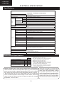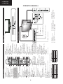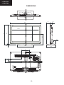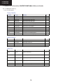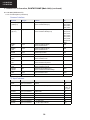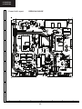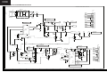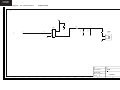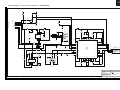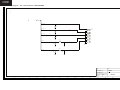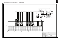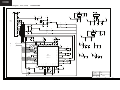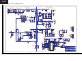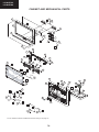
1
LC-24LE210 LC-24LE220 SERVICE MANUAL SE00LC24LE210 Issued: 05th October 2010 LED LCD COLOUR TELEVISION DVB-T / DVB-C (HDTV), PAL B/G, I / SECAM B/G, D/K, L/L’ SYSTEM COLOUR TELEVISION MODELS LC-24LE210E LC-24LE220E LC-24LE210E (FCB) In the interests of user safety (required by safety regulations in some countries) the set should be restored to its original condition and only parts identical to those specified should be used. CONTENTS ELECTRICAL SPECIFICATIONS .............................................................................. 2 IMPORTANT SERVICE SAFETY PRECAUTIONS...................................................... 3 OPERATION MANUAL ............................................................................................... 6 DIMENSIONS ......................................................................................................... 10 REMOVING OF MAJOR PARTS ................................................................................................ 11 SERVICE ADJUSTMENTS ..................................................................................... 16 SOFTWARE UPDATING .................................................................................... 28 MAJOR ICs INFORMATION ..................................................................................... 29 SOURCE OF DOCUMENTATION ..................................................................................... 39 CHASSIS LAYOUT .................................................................................................. 40 WIRING DIAGRAMS ......................................................................................... 43 BLOCK DIAGRAMS ......................................................................................... 44 SCHEMATIC DIAGRAMS ......................................................................................... 47 PRINTED WIRING BOARDS ..................................................................................... 63 REPLACEMENT PARTS LIST .................................................................................. 67 CABINET AND MECHANICAL PARTS .......................................................................... 74 PACKING OF THE SET ........................................................................................... 75 SHARP CORPORATION 1 This document has been published to be used for after sales service only. The contents are subject to chage without notice. LC-24LE210 LC-24LE220 ELECTRICAL SPECIFICATIONS Specifications 32” LCD COLOUR TV, Model: LC-32LE210E, LC-32LE220E, LC-24LE210E, LC-24LE210E, LC-24LE220E, LC-24LE210EFCB. LC-32LB220E, LC-32LS220E LC-24LE220E 24” LCD COLOUR Model: LCD COLOUR TV,TV, Model: Item LCD Panel 24” TFT LCD TFT LED LCD TV LED TV 24" BLACK Resolution 6.220.800 dots (1.920 x 1.080 pixels) Video Colour System TV Standard TV Functions Receiving Channel PAL/SECAM/NTSC 3.58/NTSC 4.43/PAL 60 Analogue CCIR (B/G, I, D/K, L/L’) Digital DVB-T (2K/8K OFDM)(H.264), DVB-C (Only Lx220) VHF/UHF E2–E69 ch, F2–F10 ch, I21–I69 ch, IR A–IR J ch (Digital: IR A ch–E69 ch) CATV Hyper-band, S1–S41 ch TV-Tuning System Auto Preset 999 ch: non-Nordic / 9999 ch: Nordic (ATV: 99 ch), Auto Label, Auto Sort STEREO / BILINGUAL NICAM/A2 Viewing angles H: 176°, V: 176° Audio Amplifier 6Wx2 Speaker (25 mm mmxx100 100mm) mm)x x2 2 Terminals 32” BLACK TFT LCD LED TV TV Antenna UHF/VHF 75 SERVICE Ø 3.5 mm jack (30 mm x 100 mm) x 2 Din type (Analogue & Digital) SCART SCART (AV input, RGB input, TV output, Y/C input) PC INPUT VGA (D-Sub 15pin), Ø 3.5mm jack COMPONENTS COMPONENT IN: Y/PB(CB)/PR(CR), RCA (AUDIO R/L) HDMI1 HDMI, Ø 3.5mm jack HDMI2 HDMI, Ø 3.5mm jack HDMI3 HDMI, Ø 3.5mm jack AV RCA connector (AV input) MEDIA PLAYER/ TIME-SHIFT/ USB REC USB 2.0 HOST (A type) DIGITAL AUDIO OUTPUT RCA S/PDIF digital audio output. C. I. (Common Interface) EN50221, R206001, CI+ speci cation (Only LE220) Headphones Ø 3.5 mm jack (Audio output) #ZECHç$ANISHç$UTCHç%NGLISHç%STONIANç&INNISHç&RENCHç'ERMANç'REEKç(UNGARIANç)TALIANç ,ATVIANç,ITHUANIANç.ORWEGIANç0OLISHç0ORTUGUESEç2USSIANç3LOVAKç3LOVENEç3PANISHç 3WEDISHç4URKISHç5KRAINIANç"YELORUSSIANç2OMANIAN OSD language Power Requirement AC 220–240 V, 50 Hz Power Consumption (IEC62087 Method) 30 W (0.25 (0.25 W 30W W (Standby) Standby) 85W (0.25 W Standby) Weight 4,9 Kg 6 Kg (With stand) 4,9 Kg(Without (Withoutstand), stand), 6 Kg (With stand) 8,5 Kg (Without stand), 9,8 Kg (With stand) Operating Temperature 0 °C to +40 °C Environmental Specifications *1 Measured according to IEC 62087 Ed. 2. *2 For further information about the Energy Save function, please see related pages in this operation manual. *3 Measured according to IEC 62301 Ed. 1. *4 Measured according to IEC 62301 Ed. 1. *5 Annual energy consumption is calculated on the basis of the On-Mode (HOME MODE) power consumption, watching TV 4 hours a day, 365 days a year. *6 Annual energy consumption is calculated on the basis of the Energy-Save-Mode power consumption, watching TV 4 hours a day, 365 days a year. 24” 25 W *1 On-Mode (W) (HOME MODE) *2 Energy-Save-Mode (W) ECO 22 W 0.25 W *3 Standby-Mode (W) *4 Off Mode (W) 0.18 W *5 Annual Energy Consumption (kWh) 37 kWh *6 Annual Energy Consumption Energy-Save-Mode (kWh) ECO 31 kWh Cautions regarding use in high and low temperature environments • When the unit is used in a low temperature space (e.g. room, office), the picture may leave trails or appear slightly delayed. This is not a malfunction, and the unit will recover when the temperature returns to normal. • Do not leave the unit in a hot or cold location. Also, do not leave the unit in a location exposed to direct sunlight or near a heater, as this may cause the cabinet to deform and the LCD panel to malfunction. Storage temperature: –20°C to +60°C. 2 • As a part of our policy of continuous improvement, SHARP reserves the right to make design and specification changes for product improvement without prior notice. The performance specification figures indicated are nominal values of production units. There may be some deviations from these values in individual units. LC-24LE210 LC-24LE220 IMPORTANT SERVICE SAFETY PRECAUTION Service work should be performed only by qualified service technicians who are thoroughly familiar with all safety checks and the servicing guidelines which follow: WARNING 1. For continued safety, no modification of any circuit should be attempted. 2. Disconnect AC power before servicing. CAUTION: FOR CONTINUED PROTECTION AGAINST A RISK OF FIRE REPLACE ONLY WITH SAME TYPE F101 (T2.5AH / 250V) BEFORE RETURNING THE RECEIVER (Fire & Shock Hazard) Before returning the receiver to the user, perform the following safety checks: 1. Inspect all lead dress to make certain that leads are not pinched, and check that hardware is not lodged between the chassis and other metal parts in the receiver. 2. Inspect all protective devices such as non-metallic control knobs, insulation materials, cabinet backs, adjustment and compartment covers or shields, isolation resistor-capacitor networks, mechanical insulators, etc. 3. To be sure that no shock hazard exists, check for leakage current in the following manner. • Plug the AC cord directly into a 220~240 volt AC outlet. (Do not use an isolation transformer for this test). •Using two clip leads, connect a 1.5k ohm, 10 watt resistor paralleled by a 0.15μF capacitor in series with all exposed metal cabinet parts and a known earth ground, such as electrical conduit or electrical ground connected to an earth ground. •A true RMS reading multimeter should be used for this test, especially where the equipment uses a switch mode power supply which may result in very non-sinusoidal leakage current. •Connect the resistor connection to all exposed metal parts having a return to the chassis (antenna, metal cabinet, screw heads, knobs and control shafts, escutcheon, etc.) and measure the AC voltage drop across the resistor. All checks must be repeated with the AC cord plug connection reversed. (If necessary, a nonpolarized adaptor plug must be used only for the purpose of completing these checks.) Any reading of 1.05V peak (this corresponds to 0.7 mA. peak AC.) or more is excessive and indicates a potential shock hazard which must be corrected before returning the monitor to the owner. DVM AC SCALE 1.5k ohm 10W 0.15 μF TEST PROBE TO EXPOSED METAL PARTS CONNECT TO KNOWN EARTH GROUND SAFETY NOTICE Many electrical and mechanical parts in LCD television have special safety-related characteristics. These characteristics are often not evident from visual inspection, nor can protection afforded by them be necessarily increased by using replacement components rated for higher voltage, wattage, etc. Replacement parts which have these special safety characteristics are identified in this manual; electrical components having such features are identified by “ ! “. For continued protection, replacement parts must be identical to those used in the original circuit. The use of a substitute replacement parts which do not have the same safety characteristics as the factory recommended replacement parts shown in this service manual, may create shock, fire or other hazards. 3 LC-24LE210 LC-24LE220 PRECAUTIONS FOR USING LEAD-FREE SOLDER 1 Employing lead-free solder “ALL PWB” of this model employs lead-free solder. The LF symbol indicates lead-free solder, and is attached on the PWBs and service manuals. The alphabetical character following LF shows the type of lead-free solder. Example: LFa Indicates lead-free solder of tin, silver and copper. LFn Sn-Ag-Ni Indicates lead-free solder of tin, silver and nickel. 2 Using lead-free wire solder When fixing the PWB soldered with the lead-free solder, apply lead-free wire solder. Repairing with conventional lead wire solder may cause damage or accident due to cracks. As the melting point of lead-free solder (Sn-Ag-Cu) is higher than the lead wire solder by 40°C, we recommend you to use a dedicated soldering bit, if you are not familiar with how to obtain lead-free wire solder or soldering bit, contact our service station or service branch in your area. 3 Soldering As the melting point of lead-free solder (Sn-Ag-Cu) is about 220°C which is higher than the conventional lead solder by 40°C, and as it has poor solder wettability, you may be apt to keep the soldering bit in contact with the PWB for extended period of time. However, Since the land may be peeled off or the maximum heat-resistance temperature of parts may be exceeded, remove the bit from the PWB as soon as you confirm the steady soldering condition. Lead-free solder contains more tin, and the end of the soldering bit may be easily corroded. Make sure to turn on and off the power of the bit as required. If a different type of solder stays on the tip of the soldering bit, it is alloyed with lead-free solder. Clean the bit after every use of it. When the tip of the soldering bit is blackened during use, file it with steel wool or fine sandpaper. Be careful when replacing parts with polarity indication on the PWB silk. Lead-free wire solder for servicing. 4 LC-24LE210 LC-24LE220 END OF LIFE DISPOSAL A. Information on Disposal for Users (private households) 1. In the European Union Attention: If you want to dispose of this equipment, please do not use the ordinary dust bin! Attention: Your product is marked with this symbol. It means that used electrical and electronic products should not be mixed with general household waste. There is a separate collection system for these products. Used electrical and electronic equipment must be treated separately and in accordance with legislation that requires proper treatment, recovery and recycling of used electrical and electronic equipment. Following the implementation by member states, private households within the EU states may return their used electrical and electronic equipment to designated collection facilities free of charge*. In some countries* your local retailer may also take back your old product free of charge if you purchase a similar new one. *) Please contact your local authority for further details. If your used electrical or electronic equipment has batteries or accumulators, please dispose of these separately beforehand according to local requirements. By disposing of this product correctly you will help ensure that the waste undergoes the necessary treatment, recovery and recycling and thus prevent potential negative effects on the environment and human health which could otherwise arise due to inappropriate waste handling. 2. In other Countries outside the EU If you wish to discard this product, please contact your local authorities and ask for the correct method of disposal. For Switzerland: Used electrical or electronic equipment can be returned free of charge to the dealer, even if you don’t purchase a new product. Further collection facilities are listed on the homepage of www.swico.ch or www.sens.ch. B. Information on Disposal for Business Users 1. In the European Union If the product is used for business purposes and you want to discard it: Please contact your SHARP dealer who will inform you about the take-back of the product. You might be charged for the costs arising from take-back and recycling. Small products (and small amounts) might be taken back by your local collection facilities. For Spain: Please contact the established collection system or your local authority for take-back of your used products. 2. In other Countries outside the EU If you wish to discard of this product, please contact your local authorities and ask for the correct method of disposal. The battery supplied with this product contains traces of Lead. For EU: The crossed-out wheeled bin implies that used batteries should not be put to the general household waste! There is a separate collection system for used batteries, to allow proper treatment and recycling in accordance with legislation. Please contact your local authority for details on the collection and recycling schemes. For Switzerland: The used battery is to be returned to the selling point. For other non-EU countries: Please contact your local authority for correct method of disposal of the used battery. 5 When one of the 5 Nordic countries (Sweden, Norway, Finland, Denmark or Iceland) is selected in the country setting of Auto Installation, DTV channels are 4 digits. When another country is selected, DTV channels are 3 digits. B Standby/On Enter standby mode or turn on the power. p Channel information / EPG (See pages 11 and 22.) MEDIA PLAYER Display the MEDIA PLAYER screen. 0–9 Set the channel in TV mode. Set the page in Teletext mode. 6 12 m Teletext ATV: Select the TELETEXT mode (See page 12.) DTV/CADTV: Select DTV/CADTV (MHEG-5) data broadcasting or TELETEXT. 13 FAV Shows the favourite list. 14 3 Freeze / Hold Freeze a picture (TV) or the Teletext on the screen (See page 12) 15 SLEEP Set the sleep timer on (in units of 10 min. up to max. 4 hr) and off. 16 REC LIST Shows list of recorded programs. (See page 28.) *CADTV only Lx220 series. 17 e Mute Switch the sound on and off. 18 2 Audio mode Select the sound multiplex mode. (See below.) 19 i (+/-) Volume i (+) Increase the volume. i (-) Decrease the volume. 20 P (r/s) TV/DTV/CADTV: Select the program or move up or down the channel list pages. Input source: Switch to TV or DTV or CADTV input mode. Teletext: Move to the next/previous page. 21 b Input source Select an input source. (See page 10.) 22 RADIO DTV/CADTV: Switch between RADIO and digital mode. •Due to the large variation in transmitted volume levels in RADIO mode, some stations will produce distortion if the volume level is set too high. 23 PC Select PC input source (Analogue connection, see page 16.) 24 MENU Display the MENU screen. (See page 18.) 25 REC Starts the USB REC recording. 26 Colour (Red/Green/Yellow/Blue) TELETEXT: Select a page. (See page 12.) DTV/CADTV: The coloured buttons are used to select correspondingly to the coloured items in the menu screen. 27 [ Subtitle for Teletext ATV: Subtitles on / off. DTV/CADTV: Display the subtitle selection screen. (See page 10 and 12.) 28 k Reveal hidden Teletext (See page 12.) 29 v Top/Bottom/Full Switch the Teletext image to Top, Bottom or Full. 30 1 Subpage (See page 12.) NICAM STEREO, MONO NICAM CH A, NICAM CH B, NICAM CH AB, MONO NICAM MONO, MONO Stereo Bilingual Monoaural CH A, CH B, CH AB MONO Monoaural STEREO, MONO Bilingual Stereo Selectable items Signal Selectable items A2 TV broadcasts selection Signal NICAM TV broadcasts selection Analogue TV mode: Each time you press 2, the mode switches as illustrated in the following tables: DTV/CADTV mode: Press 2 to open the multi audio screen. (See page 10.) • Using 2 on the remote control unit A Flashback Press to return to the previous selected channel or external input mode. 6 DTV Change between ATVļDTV or ATVļ CADTV* mode. 7 f Picture format Change between different picture formats (see page 23.) / TimeShift / Play-Pause 8 Activate or deactivate the TimeShift. Start / stop the reproduction. 9 a/b/c/d (Cursor) TV mode: Select a desired item on the setting screen. S/V USB REC and TimeShift mode: Rewind and fast forward. T/L Rewind and forward the recording in units of 5 minutes. OK Execute a command within the menu screen. ATV/DTV or ATV/CADTV mode: Display the channel list. (See page 22.) 10 END Exit the menu screen. 11 EPG DTV/CADTV: To display EPG (Electronic Programme Guide) screen. (See page 11.) 5 4 3 2 1 Remote control unit 1 2 3 4 5 USB terminal COMPONENTS / AV terminals HEADPHONES jack SCART (AV/RGB, Y/C Input) terminal PC Input i(k/l) (Volume buttons) 6 7 8 9 10 Antenna input terminal DIGITAL AUDIO OUTPUT terminal SERVICE connector (jack 3.5mm) HDMI 1 (HDMI/DVI) HDMI 2 (HDMI/DVI) P(r/s) (Programme (channel) buttons) b (INPUT SOURCE button) (MENU button) a (Power button) Remote control sensor TV (Top and rear view) TV (Front view) 11 HDMI 3 (HDMI/ DVI) 12 AUDIO input for DVI and PC. 13 COMMON INTERFACE slot 14 AC INPUT terminal B (Standby/On) indicator LC-24LE210 LC-24LE220 OPERATION MANUAL Insert two supplied “AA” size batteries. • Place batteries with their terminals corresponding to the (+) and (-) indications in the battery compartment. Close the battery cover. 2 3 7 ° Remote control sensor • Do not expose the remote control unit to shock. In addition, do not expose the remote control unit to liquids, and do not place in an area with high humidity. • Do not install or place the remote control unit under direct sunlight. The heat may cause deformation of the unit. • The remote control unit may not work properly if the remote control sensor of the TV is under direct sunlight or strong lighting. In such cases, change the angle of the lighting or the TV, or operate the remote control unit closer to the remote control sensor. Cautions regarding the remote control unit ° Use the remote control unit by pointing it towards the remote control sensor. Objects between the remote control unit and sensor may prevent proper operation. Using the remote control unit Note on disposing batteries: The batteries provided contain no harmful materials such as cadmium, lead or mercury. Regulations concerning used batteries stipulate that batteries may no longer be thrown out with the household rubbish. Deposit any used batteries free of charge into the designated collection containers set up at commercial businesses. CAUTION Improper use of batteries can result in chemical leakage or explosion. Be sure to follow the instructions below. • Do not mix batteries of different types. Different types of batteries have different characteristics. • Do not mix old and new batteries. Mixing old and new batteries can shorten the life of new batteries or cause chemical leakage in old batteries. • Remove batteries as soon as they have worn out. Chemicals that leak from batteries can cause a rash. If you find any chemical leakage, wipe thoroughly with a cloth. • The batteries supplied with this product may have a shorter life expectancy due to storage conditions. • If you will not be using the remote control unit for an extended period of time, remove the batteries from it. Hold in the tab on the battery cover and pull the cover towards the direction of the arrow. 1 Before using the TV for the first time, insert two supplied “AA” size zinc-carbon batteries. When the batteries become depleted and the remote control unit fails to operate, replace the batteries with new “AA” size batteries. Inserting the batteries Preparation Product shape varies in some countries. (Page 8). p Connect the AC cord to the TV into the CI slot to watch scrambled broadcasts (Page 8.) o If necessary, insert a CA card the antenna terminal (Page 8). n Connect an antenna cable to Preparation 1 3 Watch TV Store Start searching channels Home 9TV Location setting 9Language, country and tune type setting (Page 9). o Run the initial auto installation audio devices such as speakers/amplifier as instructed (Pages 14 and 15). o Connect external devices such as a DVD player/recorder as instructed (Pages 14 and 15). n Connect external Connect external devices antenna to attain maximum signal reception (Page 9). n Turn on the power using a on n Congratulations! Now you can watch TV. the TV (Page 10). o If necessary, adjust the Power on and run the auto installation 2 Follow the steps below one by one when using the TV for the first time. Some steps may not be necessary depending on your TV installation and connection. Initial installation overview Quick guide LC-24LE210 LC-24LE220 Operation Manual (Continued) 8 HDMI device (Page 14) Game console or camcorder (Page 14) Video recording device (Pages 14 and 15) Audio device (Page 15) ø 3.5 mm stereo mini jack cable DVI/HDMI Cable HDMI-certified cable HDMI-certified cable AV cable Audio cable Components cable SCART cable Audio cable or Audio cable NOTE • The cables illustrated in pages 13, 14 and 15 are commercially available items. The TV is equipped with the terminals as shown below. Find the cable corresponding the TV’s terminal and connect the device. Introduction to connections • Be sure to turn off the TV and any devices before making any connections. • Firmly connect a cable to a terminal or terminals. • Carefully read the operation manual of each external device for possible connection types. This also helps you get the best possible audiovisual quality to maximise the potential of the TV and the connected device. E Before connecting ... Connecting external devices ø 3,5 mm stereo mini jack cable DVI/HDMI Cable HDMI-certified cable AUDIO IN HDMI (DVI) HDMI 1, 2 or 3 PC ø 3,5 mm stereo mini jack cable VGA cable Analogue Connection Ɣ When a PC is connected to the TV with a DVI cable, it will be necessary to connect a mini stereo connector of ø 3.5mm of the TV to PC as indicated in the previous drawing. Ɣ If after connecting a PC to the TV through a HDMI cable, the audio does not run, connect a mini stereo connector of ø 3.5mm between TV and PC as indicated in the previous drawing. Ɣ After connection PC PC HDMI (DVI) Connection PC connection Connecting a PC ø 3,5 mm stereo mini jack cable DVI/VGA Conversion cable Displays an image with the same number of pixels on the screen Dot by Dot • You can also select an item by pressing f on the remote control unit. • Connect the PC before making adjustments. • Selectable picture size may vary with input signal type. • The “Aspect ratio” adjustment is only available for analogue signals through the “PC IN” terminal. NOTE An image fully fills the screen Full Item Keeps the original aspect ratio in a full screen display Full Normal 4:3 Normal Example Press Ź key to select the desired item. 2 3 Press MENU on the remote control. Press ź key to select “Aspect ratio”. 1 You can select the picture size. Selecting the picture size • When using the PC-IN terminal is necessary to connect a audio cable. NOTE PC LC-24LE210 LC-24LE220 Operation Manual (Continued) 9 • Do not connect and disconnect a USB device from the TV repeatedly. • Compatibility with USB hard disc connection. • Do not disconnect a USB device or memory card from the TV while transferring files, using the slide show function, when a screen is switching to another or before you exit “MEDIA PLAYER” from the “INPUT SOURCE” menu. • File names over 80 characters (may vary depending on character set) may not be displayed. • Use only alphanumeric characters for naming files. • Depending on the USB device, the TV may not be able to recognise the contained data. Connect an USB device to the TV as shown below. Connecting a USB device (Media Player) • Check the operations manual of the external equipment for the signal type. • If no (colour) image is displayed, try changing to another signal type. For selecting the input type of external equipment. Input source settings 1 Select PHOTO mode and press OK. 2 Select the file you want to display on full screen with Ÿ/ź /Ż/Ź buttons and press OK to start the viewing. You can reproduce photos with JPEG (*.JPE, *.JPG), BMP and PNG format on your TV. Several kinds of reproduction are possible. PHOTO mode 2 Press Ÿ/ź/Ż/Ź to select the folder where you want to search the files and then press OK. 1 Pressing Ż/Ź buttons you can change between different modes: PHOTO, MUSIC, MOVIE or TEXT. Press OK to select the option you want to reproduce. After selecting Media Player, the TV loads USB device files, and shows the following screen: MEDIA PLAYER function Troubleshooting Setting when using external devices • Is the volume too low? • Make sure that headphones are not connected. • Check if you pressed e on the remote control unit. • This is not a malfunction. This happens when the cabinet slightly expands and contracts according to changes in temperature. This does not affect the TV’s performance. • No sound. • The TV sometimes makes a cracking sound. • This TV should be fixed on a wall only with the wall fix bracket available from SHARP (Page 5). The use of other wall fix brackets may result in an unstable installation and may cause serious injuries. • Fixing the LCD colour TV requires special skills and should only be performed by qualified service personnel. Customers should not attempt to do the work themselves. SHARP bears no responsibility for improper fixing or fixing that results in accident or injury. • You can ask qualified service personnel about using an optional bracket to fix the TV on a wall. • To use this TV fixed on a wall, first remove the adhesive tape at the two locations on the rear of the TV, and then use the screws supplied with the wall fix bracket to secure the bracket to the rear of the TV. • When you fix the TV on a wall, you should attach the supporting post. Fixing the TV on a wall The copyrights for the software components and various relevant documents included with this product that were developed or written by SHARP are owned by SHARP and are protected by the Copyright Act, international treaties, and other relevant laws. This product also makes use of freely distributed software and software components whose copyrights are held by third parties. The software included in this product is comprised of various software components whose individual copyrights are held by SHARP or by third parties. Software developed by SHARP and/or third part Software composition Information on the software license for this product • When the TV is used in a low temperature space (e.g. room, office), the picture may leave trails or appear slightly delayed. This is not a malfunction, and the TV will recover when the temperature returns to normal. • Do not leave the TV in a hot or cold location. Also, do not leave the TV in a location exposed to direct sunlight or near a heater, as this may cause the cabinet to deform and the LCD panel to malfunction. Storage temperature: -20 °C to e60 °C. Cautions regarding use in high and low temperature environments Are connections to external equipment correct? (Pages 13, 14 and 15) Is the input signal type selected correctly after connection? (Page 10) Is the correct input source selected? (Page 10) Is the picture adjustment correct? (Pages 19) Is the antenna connected properly? (Page 8) • • • • • • No picture. • Adjust the picture tone. • Is the room too bright? The picture may look dark in a room that is too bright. • Check the “PICTURE” setting (Page 19). • Strange colour, light colour, or dark colour, or colour misalignment. • The TV’s internal temperature has increased. Remove any objects blocking the vent or clean. • Is the “Sleep Timer” set? Select “Off” from the “TIME” menu (Page 20). • Is “No Signal Off” or “No operation Off” activated? • Is the image position correct? • Are screen mode adjustments (Aspect ratio) such as picture size made correctly? (Page 23.) • Picture is cut off. • Power is suddenly turned off. • • • • • Remote control unit does not operate. Are batteries inserted with polarity (e, f) aligned? Are batteries worn out? (Replace with new batteries.) Are you using it under strong or fluorescent lighting? Is a fluorescent light illuminating to the remote control sensor? • External influences such as lightning, static electricity, etc., may cause improper operation. In this case, operate the TV after first turning off the power, or unplugging the AC cord and re-plugging it in after one or two minutes. • The TV cannot be operated. Possible Solution • Check if you pressed B on the remote control unit. If the indicator on the TV lights up red, press B. • Is the AC cord disconnected? • Check if you pressed a on the TV. • No power. Problem Appendix Other useful features LC-24LE210 LC-24LE220 Operation Manual (Continued) LC-24LE210 LC-24LE220 DIMENSIONS 87 587 40 245 293.7 377 415 521.8 38 62 390 216 60 75 75 10 LC-24LE210 LC-24LE220 REMOVING OF MAJOR PARTS 1. To slacken the 4 lock screws 2. Remove the 2 lock screws 2 1 and detach the Stand. , 2 lock screws 3 , 3 lock screws 4 , 1 lock screw 5 and detach the Rear Cabinet 5 Rear Cabinet 4 2 3 Stand Front Cabinet 11 LC-24LE210 LC-24LE220 Removing of major parts (Continued) 3. Disconnect all the connectors from all the PWBs. 4. Remove the Key Unit Ass’y 6 . Control cover 6 Control button [KM] KEY UNIT [LV] [SP] [LA] [LV] [PD] [PD] [RA] [LA] SP-R [RA] SP-L 12 [KM] LC-24LE210 LC-24LE220 Removing of major parts (Continued) 5. Remove the speaker (R) 7 , (L) 8 . 6. Remove the 4 lock screws 9 , and detach the POWER Unit. 7. Remove the 2 lock screws 10 , and detach the MAIN Unit. 8. Remove the LED PWB 11 . 9 MAIN Unit 10 POWER Unit 7 Speaker (R) LED PWB 13 Speaker (L) 11 8 LC-24LE210 LC-24LE220 Removing of major parts (Continued) 9. Remove the 2 lock screws 12 and detach the stand angle. 12 14 LC-24LE210 LC-24LE220 Removing of major parts (Continued) 10. Remove the 4 lock screws 13 . 12. Remove the 4 lock screws 14 . and detach the angles. 14 14 13 13 14 13 13 15 LC-24LE210 LC-24LE220 SERVICE ADJUSTMENTS 1. Adjustment method after PWB and/or IC replacement due to repair The unit is set to the optimum performance at the time of shipment from the factory. If any value should become improper or any adjustment is necessary due to the part replacement, make an adjustment according to the following procedure. 1.1. Procure the following units in order to replace the main unit: MAIN UNIT DUNTKF639FMxx NOTE: [Caution when replacing ICs in the main unit (IC1901, IC1902, IC1902, IC1501, IC1006 and IC1007)] Before replacing the relevant part, procure the following parts in which the data have been rewritten. Ref. Description Parts code IC + data Description new IC code for service IC1901 HDMI EDID 1 RH-IXD236WJZZY RH-IXD080WJZZY AND DATA LC32LE2x0E_HDMI_1_EDID IC1902 HDMI EDID 2 RH-IXD237WJZZY RH-IXD080WJZZY AND DATA LC32LE2x0E_HDMI_2_EDID IC1903 HDMI EDID 3 RH-IXD238WJZZY RH-IXD080WJZZY AND DATA LC32LE2x0E_HDMI_3_EDID IC1501 PC EDID RH-IXD239WJZZY RH-IXD080WJZZY AND DATA LC32LE2x0E_PC_EDID IC1006 HDCP USER SETTINGS RH-IXD261WJZZY RH-IXC986WJZZY AND DATA LC32LE2x0E_HDCP_KEY IC1007 * FLASH MEMORY RH-IXD274WJZZY RH-IXD012WJZZY and 24LE210_v1.12_PANEL_CMI * For LE220 models it is not possible replace IC1007. Replace the full Main Unit. 2. Entering and exiting the adjustment process mode. Standard method. 1. By key-unit. 1. Unplug the AC power cord. 2. Press and hold “V-” and “b” keys, simultaneously, and then plug the AC power cord. 3. “K” appears on the screen. 4. Press and hold “V-” and “P-” keys, simultaneously. 5. “SHARP FACTORY MENU” appears (see Figure 1). 6. Unplug the AC power cord to exit of adjustments process. 2. By own R/C 1. Turn on the TV set. 2. Press “b”,”2”,”5”, “8”, “0” (the time is limited to 5 sec. approx., for enter this code). 3. “SHARP FACTORY MENU” appears (see Figure 1). 4. Press “OK” on lines 5 ~ 12 to go to submenu. 5. Press “MENU” to return to main menu. 6. Press “END” to exit of adjustments mode. 16 LC-24LE210 LC-24LE220 3. Remote control key operation and description of display in adjustment process mode. 1. key operation Remote control key Keyboard unit Function P (s/r) Moving an item (line) by one (up/down) on “Sharp Factory Menu” or submenus. b Selecting a submenu on lines 5 to 12 of “Sharp Factory Menu” or executing a function. Cursor (▼/▲ ) OK Cursor (◄/►) V (+/-) Changing a selected item setting value. MENU MENU Return to “Sharp Factory Menu” from a submenu. The required input mode should be switched previously to enter the Service Mode. CAUTION: Use due care in handling the information described here lest the users should know how to enter the adjustment process mode. If the settings are tampered with in this mode, unrecoverable system damage may result. 4. Description of display (1) Figure 1: Main Service Adjustment Menu SHARP FACTORY MENU Main version 2 210 SHARP S 1 12 SEES S S v94 9 MSTAR S C 30 3088 13 24LE210E v1.12 CL308413 Bootloader version Error standby cause ← Informative. BD_MST064E_C01A 2 Normal standby cause ← Informative (Main microprocessor version). ← Informative (Remote Control/Keyboard…). Remote control ← Informative (None/Lamp Error). None INIT ← Press “OK” to go to INIT submenu. ADJUST ← Press “OK” to go to ADJUST submenu. ETC ← Press “OK” to go to ETC submenu. PUBLIC MODE ← Press “OK” to go to PUBLIC MODE submenu. SMARTLOADER ← Press “OK” to go to SMARTLOADER submenu. ADC ADJUST ← Press “OK” to go to ADC ADJUST submenu. GAMMA ← Press “OK” to go to GAMMA submenu. SYSTEM INFORMATION ← Press “OK” to go to SYSTEM INFORMATION submenu. No. Description (2) (3) Display specification (1) Service Information Current Software version and others. (2) Item name Submenus to be checked or adjusted (by pressing “OK” button) (3) Factory init and Inch setting Are shown on INIT submenu 17 LC-24LE210 LC-24LE220 5. Adjustment process mode menu Page Line Sub Item 01/17 [SHARP FACTORY MENU Description Remarks (adjustment details, etc.) Page 1 Main Version 2 Bootloader Version 3 Normal Standby Cause 4 Error Standby Cause 5 INIT 02/17 24LE210E SHARP v1.12 SEES v94 MSTAR CL308413 BD_MST064E_C01A 2 Informative only No signal Informative only None Informative only Factory Init Submenu Factory Init EURO Inch Setting CMO_M236H3-LA2 Center Acutime 0H0M ADJUST 03/17 04/17 INPUT SOURCE (1/6) Informative (EURO/RUSSIA/SWEDEN/UK/EAST EUROPE) Panel type Backlight ON accumulated Time QMAP ADJUST Submenu Press “OK” to enter to QMAP ADJUST Submenu RF_PAL_BGHI AFEC Only for Engineering purpose (Please don’t use) Comb Only for Engineering purpose (Please don’t use) SECAM Only for Engineering purpose (Please don’t use) SCinit Only for Engineering purpose (Please don’t use) CSC OFF Only for Engineering purpose (Please don’t use) CSC_Dither OFF Only for Engineering purpose (Please don’t use) YCdelay OFF Only for Engineering purpose (Please don’t use) PreFilter OFF Only for Engineering purpose (Please don’t use) HSD_Y ALL PASS1X Only for Engineering purpose (Please don’t use) HSD_C ALL PASS1X Only for Engineering purpose (Please don’t use) VSD OFF Only for Engineering purpose (Please don’t use) CTI CTI_1 Only for Engineering purpose (Please don’t use) INPUT SOURCE (2/6) MemFormat 05/17 Press “OK” to enter to Factory Init Submenu Press “◄ “ or “ ►” to reset Center Acutime RESET 6 Informative only (Main microprocessor version) DTV/ RF/Multimedia ... 422MF Only for Engineering purpose (Please don’t use) 444To422 ON Only for Engineering purpose (Please don’t use) PreSNR OFF Only for Engineering purpose (Please don’t use) DNR NR_OFF Only for Engineering purpose (Please don’t use) DNR_Motion MR_NR Only for Engineering purpose (Please don’t use) DNR_Y OFF Only for Engineering purpose (Please don’t use) DNR_MED OFF Only for Engineering purpose (Please don’t use) DNR_C OFF Only for Engineering purpose (Please don’t use) PNR OFF Only for Engineering purpose (Please don’t use) PNR_Y OFF Only for Engineering purpose (Please don’t use) PNR_C OFF Only for Engineering purpose (Please don’t use) PostCCS OFF Only for Engineering purpose (Please don’t use) INPUT SOURCE (3/6) PostCCS_Smooth 420CUP MADi MADi_Motion MADi_ADP3x3 DTV/ RF/Multimedia ... PCS_6 Only for Engineering purpose (Please don’t use) OFF Only for Engineering purpose (Please don’t use) P_MODE_MOT10 Only for Engineering purpose (Please don’t use) MOT_PMODE Only for Engineering purpose (Please don’t use) OFF Only for Engineering purpose (Please don’t use) MADi_MORPHO OFF Only for Engineering purpose (Please don’t use) MADi_DFK OFF Only for Engineering purpose (Please don’t use) 18 LC-24LE210 LC-24LE220 Page Line Sub Item Description Remarks (adjustment details, etc.) Page 1/17 [SHARP FACTORY MENU 6 ADJUST (continued) 05/17 06/17 INPUT SOURCE (3/6) DTV/ RF/Multimedia ... OFF Only for Engineering purpose (Please don’t use) MADi_Force OFF Only for Engineering purpose (Please don’t use) EODi OFF Only for Engineering purpose (Please don’t use) Film SD_2 Only for Engineering purpose (Please don’t use) Film32 OFF Only for Engineering purpose (Please don’t use) INPUT SOURCE (4/6) DTV/ RF/Multimedia ... Film22 OFF Only for Engineering purpose (Please don’t use) DIPF OFF Only for Engineering purpose (Please don’t use) VCLPF ON Only for Engineering purpose (Please don’t use) Spike_NR S2 Only for Engineering purpose (Please don’t use) SPF ON Only for Engineering purpose (Please don’t use) SPF_DBK OFF Only for Engineering purpose (Please don’t use) SPF_SNR E2S1 Only for Engineering purpose (Please don’t use) ON Only for Engineering purpose (Please don’t use) LPF3x3 Only for Engineering purpose (Please don’t use) SPF_SMR S2 Only for Engineering purpose (Please don’t use) SPF_NMR_MR ON Only for Engineering purpose (Please don’t use) DMS S2 Only for Engineering purpose (Please don’t use) SPF_MR_LPF INPUT SOURCE (5/6) DTV/ RF/Multimedia ... VSP_Y SRAM_1_4Tap Only for Engineering purpose (Please don’t use) VSP_C ROM_121 Only for Engineering purpose (Please don’t use) VSP_CoRing OFF Only for Engineering purpose (Please don’t use) VSP_DeRing OFF Only for Engineering purpose (Please don’t use) VSP_Dither OFF Only for Engineering purpose (Please don’t use) VSP_PreVBound OFF Only for Engineering purpose (Please don’t use) HSP_Y SRAM_1_4Tap Only for Engineering purpose (Please don’t use) HSP_C ROM_121 Only for Engineering purpose (Please don’t use) HSP_CoRing Y_Coring_1 Only for Engineering purpose (Please don’t use) HSP_DeRing OFF Only for Engineering purpose (Please don’t use) HSP_Dither OFF Only for Engineering purpose (Please don’t use) OFF Only for Engineering purpose (Please don’t use) HnonLinear 08/17 Press “OK” to enter to QMAP ADJUST Submenu MADi_SST SPF_DBK_SNR_MR 07/17 QMAP ADJUST Submenu INPUT SOURCE (6/6) SRAM1 DTV/ RF/Multimedia ... lnvSinc4Tc4p4Fc85 Only for Engineering purpose (Please don’t use) Fstop134Apass01Astop50 SRAM2 lnvSinc6Tc4p4Fc94 Only for Engineering purpose (Please don’t use) Fstop134Apass01Astop60 422To444 ON Only for Engineering purpose (Please don’t use) Peaking 1080p Only for Engineering purpose (Please don’t use) SwDriver ALL Only for Engineering purpose (Please don’t use) VIP_CSC OFF Only for Engineering purpose (Please don’t use) VIP_CSC_Dither OFF Only for Engineering purpose (Please don’t use) Multimedia_photo_HD Only for Engineering purpose (Please don’t use) Color 3x3 OFF Only for Engineering purpose (Please don’t use) Display ALL Only for Engineering purpose (Please don’t use) Post_CON_BRI OFF Only for Engineering purpose (Please don’t use) 19 LC-24LE210 LC-24LE220 Page Line Sub Item Description Remarks (adjustment details, etc.) Page 01/17 [SHARP FACTORY MENU 7 ETC 09/17 8 Press “►” to Clear NVM data EEP Clear B Press “►” to Clear NVM data (except adjustments area). Standby cause reset “OK“ will be displayed Autoinstallation SW Off 0 Selection of internal pattern from 0 up to 6… 0 Press “►” to LAMP ERR RESET. Initialization of L_ERR. L Error Check On L_ERR detection. ON: activated. OFF: deactivated. I2C OFF Off I2C BUS status. On: free BUS. Off: Normal. Sharp protocol On Remote Control Protocol. On: SHARP Off: MSTAR. Power On fixed Volume fixed Level 60 Variable 20 Press “◄” or “►” to change Variable/Fixed. Press “◄” or “►” to change 0/60. Press “◄” or “►” to change Variable/Fixed. Press “◄” or “►” to change 0/60. Respond Press “◄” or “►” to change Respond/No respond. Respond Press “◄” or “►” to change Respond/No respond. Menu button Respond Press “◄” or “►” to change Respond/No respond. On Press “◄” or “►” to change On/Off. Input mode start Normal Press “◄” or “►” to change Normal/TV/SCART/… Input mode fixed Variable Press “◄” or “►” to change Variable/Fixed. Input TV mode program number Normal Press “◄” or “►” to change Normal → 1 → 2 ...999 → Normal). Off Press “◄” or “►” to change On/Off (required external module) PUBLIC MODE (2/2) Hotel mode PUBLIC MODE Submenu Off Press “◄” or “►” to change On/Off. Reset “OK“ will be displayed Press “◄” or “►” to return to factory settings. Execute “OK“ will be displayed Press “◄” or “►” to confirm. SMART LOADER SMART LOADER Submenu Press “OK” to enter to SMART LOADER Submenu Save settings to USB (“OK“ or “NO USB drive available, please check and/or insert USB dri...” will be displayed). Press “◄” or “►” to Save. (“OK, reboot TV set“ or “NO USB drive available, please check and/or insert USB dri...” will be displayed). Press “◄” or “►” to Load. Load settings from USB ADC ADJUST 13/17 Variable Press “OK” to enter to PUBLIC MODE Submenu Panel button RC path through 10 PUBLIC MODE Submenu RC button On screen display 12/17 On: Pending to execute on next power on. Off: Not required. L Error Reset Volume fixed 9 Press “►” to Reset of STANDBY CAUSE. Pattern Maximum volume 11/17 Press “OK” to enter to ETC Submenu EEP Clear PUBLIC MODE (1/2) 10/17 EEP, Autoinstallation, Option, Country, L Error... (“OK” or “NO USB drive available, please check and/or insert USB dri…” will be displayed). ADC ADJUST Submenu Press “OK” to enter to ADC ADJUST Submenu YPbPr(SD) Press “◄” or “►” to change RGB/YPbPr(SD)/ YPbPr(HD)/ PC-RGB. ADJUST External signal Press “◄” or “►” to change Internal signal/External signal. External: factory. Internal: service R-GAIN 80 Press “◄” or “►” for manual adjustment. G-GAIN 70 Press “◄” or “►” for manual adjustment. MODE 20 LC-24LE210 LC-24LE220 Page Line Sub Item 01/17 [SHARP FACTORY MENU Description Remarks (adjustment details, etc.) Page ADC ADJUST (continued) 10 13/17 11 14/17 80 Press “◄” or “►” for manual adjustment. R-OFFSET 128 Press “◄” or “►” for manual adjustment. G-OFFSET 128 Press “◄” or “►” for manual adjustment. B-OFFSET 128 AUTO ADC “SUCCESS” or ”Fail will be displayed 12 17/17 Press “◄” or “►” for manual adjustment. Press “◄” or “►” for automatic adjustment in each mode. GAMMA (1/3) GAMMA Submenu MGAMMA IN1 40 W/B adjustment, gradation 1 input setting. MGAMMA IN2 80 W/B adjustment, gradation 2 input setting. MGAMMA IN3 120 W/B adjustment, gradation 3 input setting. MGAMMA IN4 160 W/B adjustment, gradation 4 input setting. MGAMMA IN5 200 W/B adjustment, gradation 5 input setting. Press “OK” to enter to GAMMA Submenu 240 W/B adjustment, gradation 6 input setting. MGAMMA WRITE “SUCCESS” will be displayed Press “◄” or “►” for EEP writing of adjustment values. MGAMMA RESET “SUCCESS” will be displayed Press “◄” or “►” for Initialization of adjustment values. GAMMA (2/3) GAMMA Submenu MGAMMA R1 132 W/B adjustment, gradation 1R adjustment value. MGAMMA G1 118 W/B adjustment, gradation 1G adjustment value. MGAMMA B1 146 W/B adjustment, gradation 1B adjustment value. MGAMMA R2 276 W/B adjustment, gradation 2R adjustment value. MGAMMA G2 255 W/B adjustment, gradation 2G adjustment value. MGAMMA B2 308 W/B adjustment, gradation 2B adjustment value. MGAMMA R3 418 W/B adjustment, gradation 3R adjustment value. MGAMMA G3 385 W/B adjustment, gradation 3G adjustment value. MGAMMA B3 474 W/B adjustment, gradation 3R adjustment value. MGAMMA WRITE 16/17 Press “OK” to enter to ADC ADJUST Submenu B-GAIN MGAMMA IN6 15/17 ADC ADJUST Submenu “SUCCESS” will be displayed Press “◄” or “►” for EEP writing of adjustment values. GAMMA (3/3) W/B ADJUST Submenu MGAMMA R4 559 W/B adjustment, gradation 4R adjustment value. MGAMMA G4 520 W/B adjustment, gradation 4G adjustment value. MGAMMA B4 643 W/B adjustment, gradation 4B adjustment value. MGAMMA R5 701 W/B adjustment, gradation 5R adjustment value. MGAMMA G5 655 W/B adjustment, gradation 5G adjustment value. MGAMMA B5 807 W/B adjustment, gradation 5B adjustment value. MGAMMA R6 845 W/B adjustment, gradation 6R adjustment value. MGAMMA G6 793 W/B adjustment, gradation 6G adjustment value. MGAMMA B6 998 W/B adjustment, gradation 6R adjustment value. MGAMMA WRITE “SUCCESS” will be displayed Press “◄” or “►” for EEP writing of adjustment values. SYSTEM INFORMATION SYSTEM INFORMATION Submenu Press “OK” to enter to SYSTEM INFORMATION Submenu (Only for Engineering purpose, don’t use) NOISE LEVEL 0 Informative (changing). GLOBAL MOTION 0 Informative (changing). BIT RATE 0 Informative. Scan name search 2 Changeable between 0 and 255. VPS code FFFF Informative. 830/1 code FFFF Informative. 830/2 code FFFF Informative. Top TXT enabled 1 Press “◄” or “►” to change 0/1. CEC off Press “◄” or “►” to change off/on. 21 LC-24LE210 LC-24LE220 6. Video Signal Adjustment Procedure 6.1. RGB SCART ADC 1. Enter in Service mode. 2. Press “▼” until selecting “ADC ADJUST” option. 3. Press “OK”. 4. “ADC ADJUST” menu appears. 5. Press “▼” until selecting “ADJUST” option. 6. Press “►”until selecting “Internal Signal”. 7. Press “▲”until selecting “MODE” option. 8. Press “►”until selecting “RGB”. 9. Press “▼” until selecting “AUTO ADC” option. 10. Press “►”, the adjustment starts. 11. “SUCCESS” appears when the adjustments finish. 12. Exit of Service mode. 6.2. COMPONENTS ADC 1. Enter in Service mode. 2. Press “▼” until selecting “ADC ADJUST” option. 3. Press “OK”. 4. “ADC ADJUST” menu appears. 5. Press “▼” until selecting “ADJUST” option. 6. Press “►”until selecting “Internal Signal”. 7. Press “▲”until selecting “MODE” option. 8. Press “►”until selecting “YPbPr(SD)” or “YPbPr(HD)” 9. Press “▼” until selecting “AUTO ADC” option. 10. Press “►”, the adjustment starts. 11. “SUCCESS” appears when the adjustments finish. Note: both SD and HD are adjusted. 12. Exit of Service mode. 6.3. PC IN RGB ADC 1. Enter in Service mode. 2. Press “▼” until selecting “ADC ADJUST” option. 3. Press “OK”. 4. “ADC ADJUST” menu appears. 5. Press “▼” until selecting “ADJUST” option. 6. Press “►”until selecting “Internal Signal”. 7. Press “▲”until selecting “MODE” option. 8. Press “►”until selecting “PC-RGB”. 9. Press “▼” until selecting “AUTO ADC” option. 10. Press “►”, the adjustment starts. 11. “SUCCESS” appears when the adjustments finish. 12. Exit of Service mode. 22 LC-24LE210 LC-24LE220 7. White Balance Adjustment Condition: AV MODE= Dynamic (backlight at max.). • Adjustments reference device: Minolta CA-210 • Adjustments target: x=0.300, y=0.310 High: adjustments spec ±0.001, inspection spec: ±0.002 Low: adjustments spec ±0.002, inspection spec: ±0.004 1. Press “▼” until selecting “GAMMA” option. 2. Press “OK”. 3. “GAMMA” menu appears. 4. Press “▼” until selecting “MGAMMA RESET”. 5. Press “►”, to restore default values. 6. “MGAMMA RESET SUCCESS” appears. 7. Press “P+” to increase one page. 8. Press “1”, appears “Internal Adjustments Pattern 1”. 9. Hold the default value for “MGAMMA G1”. (Note: next, try to get the (x, y) adjustments target, changing “MGAMMA R1” and “MGAMMA B1” as follow). 10. Press “▼” until selecting “MGAMMA R1”. 11. Press “◄ ►” until you obtain the desired value. 12. Press “MENU” to return to previous menu. 13. Press “▼” until selecting “MGAMMA B1”. 14. Press “◄ ►” until you obtain the desired value. 15. Press “MENU” to return to previous menu. (Note: In case of not being possible to achieve the desired (x, y) target, try to get it by changing also the “MGAMMA G1”) 16. Press “2”, appears “Internal Adjustments Pattern 2”. 17. Repeat from step 9 to 15 for the “MGAMMA R2” and “MGAMMA B2”. 18. Press “3”, appears “Internal Adjustments Pattern 3”. 19. Repeat from step 9 to 15 for the “MGAMMA R3” and “MGAMMA B3”. 20. Press “4”, appears “Internal Adjustments Pattern 4”. 21. Repeat from step 9 to 15 for the “MGAMMA R4” and “MGAMMA B4”. 22. Press “5”, appears “Internal Adjustments Pattern 5”. 23. Repeat from step 9 to 15 for the “MGAMMA R5” and “MGAMMA B5”. 24. Press “6”, appears “Internal Adjustments Pattern 6”. 25. Repeat from step 9 to 15 for the “MGAMMA R6” and “MGAMMA B6”. 26. Press “▼” until selecting “MGAMMA WRITE”. 27. Press “►”, to save the new values. 28. “MGAMMA WRITE SUCCESS” appears. NOTE: For activating the W/B flag, only is necessary to send the order MGAMMA WRITE. After this action, the “W” W/B flag will change to “1”. 23 LC-24LE210 LC-24LE220 8. Initialization to factory setting Caution: When the factory settings have been made, all user setting data, including the channel settings, are initialized. (The adjustments done in the adjustment process mode are not initialized.) Keep this in mind when initializing these settings. 1. Enter in Service mode. 2. Press “▼” or “▲” key until selecting INIT. 3. Press OK key. 4. INIT menu appears and “Factory init” option is selected. 5. Press “◄” or “►” until selecting the option desired (EURO/RUSSIA/SWEDEN/UK/EAST EUROPE). 6. Press OK key and initialization starts. 7. OK, EURO message appears for EURO option when the setting is complete. OK, RUSSIA message appears for RUSSIA option when the setting is complete. OK, SWEDEN message appears for SWEDEN option when the setting is complete. OK, UK message appears for UK option when the setting is complete. OK, EAST EUROPE message appears for EAST EUROPE option when the setting is complete. Note: Never turn the power off during initialization. To exit the adjustment process mode, unplug the AC power cord from the outlet to forcibly turn off the power. The following settings will be back to their factory ones. • • • • User settings Channel data (e.g. broadcast frequencies) Maker option setting Password data 24 LC-24LE210 LC-24LE220 9. Lamp error detection 1. Function description This LCD colour television has a function (lamp error detection) to be turned OFF the TV set automatically for safety criteria when the lamp or lamp circuit is abnormal. If the lamp or lamp circuit is abnormal, or some other errors happen, and the lamp error detection is executed, the following occurs: a. The TV set is turned OFF automatically 20 seconds after it is turned ON by the user. (The power LED on the front side of TV turns from green to red) b. If the situation “a.” happens 5 times sequentially, it becomes impossible to turn on the power. (The power LED turns from green to red and keeps blinking in red). LED Flashing timing 1s Red → 260 ms Off → 1s 260 ms 2. Countermeasures a. Checking with [L Error Check Off]. Repair the problem that produces the LAMP ERROR. The TV remains with power LED blinking until K mode is forced by local keyboard, in order to disable the LAMP ERROR detection. To disable the LAMP ERROR feature is necessary enter in K mode by pressing “VOL DOWN” and “b” keys at same time when the AC cord is plugged in. b. Resetting the LAMP ERROR counter. After the lamp and lamp circuit are found out of trouble, the LAMP ERROR counter should be reset. If a LAMP ERROR is detected five consecutive times, the power cannot be turned on. Method 1: Using the cursor (UP/DOWN) key, move to the cursor to [L Error Reset] on Line 6 of ETC Menu Fig 4. With the cursor (LEFT/RIGHT) keys reset the value to “0”. Method 2: In the case the TV is not blocked (less than 5 consecutive errors), switch on the Set. After 30 minutes working, the LAMP ERROR counter will be reset automatically. 25 LC-24LE210 LC-24LE220 10. Public Mode (Hotel mode) 1. How to Enter in the Public Mode (Hotel Mode). There are three following ways to display the Public Mode setting screen. Method 1: Turn on the power and enter in the Service mode as usual and select line 8 [PUBLIC MODE]. Method 2: Unplug the AC power cord. While pressing “VOL+” and “b” keys at the same time, plug the AC power cord. Then, when you are asked for the password, enter “0027”. After this sequence the TV will turn on showing the Public Mode setting screen as it is shown in Fig. 5. In another case, the screen is erased, and it operates in the ordinary mode. Method 3: By special R/C code: RC table LCD, SYS CORD: 0x78, RC DATA: (HEX) 0xC7, (DEC) 199. Then, when you are asked for the password, enter “0027”. After this sequence the TV will turn on showing the Public Mode setting screen as it is shown in Fig. 5. Is possible to select each item of function by pressing cursor UP/DOWN keys on the remote control or CH (UP/ DOWN) keys on the LCD TV. The setting position of each item of functions is made by pressing cursor RIGHT/LEFT keys on the remote control or VOL (+) / (-) keys on the LCD TV. Set to ON the HOTEL MODE function to active it. Select EXECUTE position after you set all function, and press cursor RIGHT/LEFT keys on the remote control or VOL (+) / (-) keys on the LCD TV for confirmation. Unplug and plug the AC power cord to take effect all the changes. 2. Public Mode Settings. 1. POWER ON FIXED [VARIABLE ↔ FIXED] When it is set to “FIXED” the TV is impossible to be switch off by Main Switch or Remote Control. 2. MAXIMUM VOLUME [0 ↔ 60] Is possible to set the maximum volume at limited level. 3. VOLUME FIXED [VARIABLE ↔ FIXED] Is possible to fix the sound volume at limited level. When “FIXED” is selected the sound volume before limited is fixed. 4. VOLUME FIXED LEVEL [0 ↔ 60] If “FIXED” has been selected, is possible to set a fixed volume at the level that is chosen. 5. RC BUTTON [RESPOND ↔ NO RESPOND] If “NO RESPOND” is selected, the remote control keys are inoperative. 6. PANEL BUTTON [RESPOND ↔ NO RESPOND] If “NO RESPOND” has been selected, the set’s keys remain deactivated (Except POWER key). 7. MENU BUTTON [RESPOND ↔ NO RESPOND] If “NO RESPOND” has been selected, “MENU” key, of remote control, is inoperative. 26 LC-24LE210 LC-24LE220 10. Public Mode (Hotel mode) (continued) 8. ON SCREEN DISPLAY [On ↔ Off] If “NO” has been selected, the On Screen Display does not appear. 9. INPUT MODE START [NORMAL → TV → SCART → COMPONENTS → HDMI1 → HDMI2 → HDMI3 → AV →MEDIA PLAYER] When any other item than “NORMAL” has been selected, the sets will start in a selected input mode at the next power-on. 10. INPUT MODE FIXED [VARIABLE → FIXED] “FIXED” has been selected, any channels and input modes other than those selected at the start mode cannot be picked up. 11. INPUT TV MODE PROGRAM NUMBER [NORMAL → 1-999 → NORMAL] When any other item than “NORMAL”, i.e. number, has been selected, and “INPUT MODE START” option is set to “TV”, the sets will start in the selected service / program number at the next power-on. 12. RC PATH THROUGH [ON ↔ OFF] T.B.D. 13. HOTEL MODE [ON ↔ OFF] If ON has been selected the HOTEL MODE is activated. 14. RESET Cancel all Public Mode settings. (It returns to the factory settings) 15. EXECUTE Select this item, and press cursor RIGHT / LEFT keys on the remote control or VOL (+) / (-) keys on the LCD TV for confirmation the functions settings. 11. SMART LOADER Description. The Smartloader is a function implemented in the service software of SEES designed LE200 series intended to easily replicate the user settings of one TV into another. These settings include (but not restricted to): picture and audio, tuning set-up, language and country selection, PIN, child locked programs… Factory adjustments are not copied as they are different for every TV. The Smartloader makes possible the user data to be stored in a memory device connected to the USB terminal of the TV that is used as reference and later load those data into other TVs by using their respective USB terminal. How it works. In reference TV: 1. Insert a memory device in the USB slot. 2. Enter in service mode, select Factory Menu and SMARTLOADER option. 3. Select “Save settings to USB” and press the RIGHT cursor in the remote control. 4. Wait until “OK” is displayed, the file has been successfully created in the root directory of the memory device. In case of error, an explanation message is shown. In TV to be cloned: 1. Insert a memory device with a file in it obtained following the above procedure. 2. Enter in service mode, select Factory Menu and SMARTLOADER option. 3. Select “Load settings from USB” and press the RIGHT button in the remote control. 4. After some seconds, “OK, reboot TV set” is displayed. In case of error, an explanation message is shown. 5. As indicated, reboot the TV to load the new settings. Very important: All the TVs must have the same software version and hardware. 27 Ɣ LC-24LE210 LC-24LE220 Ɣ Ɣ 1. Introduction SOFTWARE UPDATING Ɣ 1. In order to proceed with the Software Updating do not enter into Service Mode. Ɣ 2. The TV should be in normal operation (ON). 2. Procedure 1. Insert the USB memory into the USB terminal with the file name “MERGE.bin”(for LE210) or “MERGE_aes.bin”(for LE220) on the root directory. 2. Press “MENU”. • “PICTURE” menu appears on screen. 3. Press “►” until selecting “OPTION” menu. 4. Press “▼” until selecting “Software update (USB) Sharp v*.*”. • The current software version is displayed. 5. Press “OK” • “Are you sure? Yes - No” message is displayed. 6. Press “◄” until selecting “Yes”. 7. Press “OK”. • The software update process starts. • “Software upgrading… **%” message appears. • The upgrading process is finished, the LCD-TV restarts. NOTE: If the “MERGE.bin” (for LE210) or “MERGE_aes.bin”(for LE220) on the USB memory is not the proper for this model, an ERROR message is shown on screen and the LCD TV restarts itself. No upgrade is made. 8. Remove the AC cord and plug it again. 9. Return to OPTION menu to check that the version has been updated successfully. NOTE: If the TV is switched off during the upgrade process, when it is switched on again, the Power LED flashes: Violet for 130 ms and blue for 1.5 s, with NO screen until it is detected in the USB memory a file “MERGE.bin”(for LE210) or “MERGE_aes.bin” (for LE220). Then the power LED will flash: Violet for 40 ms and blue for other 40 ms, with NO screen while the new software is uploaded. Once the process is completed, the TV set will start automatically. 28 LC-24LE210 LC-24LE220 MAJOR ICs INFORMATION 1. General ICs Information Main Unit ICs: • IC 201 (LE210): Digital DVBT / VIF Demodulator Part number: MSB1220LQFP Sharp code: RH-IXC868WJZZQ The MSB1220-LF is a DVB-T demodulator. It is fully compliant with the DVB-T (ETSI ET 300 744), D-Book 5.0 and Nordig unified specification. Converts IF differential signals to MPEG-2/4 transport stream format. It can be used in all 2k, 4k and 8 k modes. The device includes a high performance 11 bit A/D converter capable of accepting direct IF at 36 or 44 Mhz. A digital filter with high rejection capability is also cope with digital or analog adjacent channel. The frequency capture range is sufficient to compensate for the combined offset introduced by the tuner and broadcaster without reprogramming the tuner. • IC 201 (LE220): Digital DVBT / VIF Demodulator Part number: MSB1222-LF Sharp code: RH-IXD148WJZZQ The MSB1222-LF is a DVB-T/DVB-C demodulator. It is fully compliant with the DVB-T (ETSI ET 300 744), D-Book 5.0 and Nordig unified specification. Also is compliant with DVB-C (EN 300429) and ITU-T J.83 Annex A/C. Converts IF differential signals to MPEG-2/4 transport stream format. It can be used in all 2k, 4k and 8 k modes. The device includes a high performance 11 bit A/D converter capable of accepting direct IF at 36 or 44 Mhz. A digital filter with high rejection capability is also cope with digital or analog adjacent channel. The frequency capture range is sufficient to compensate for the combined offset introduced by the tuner and broadcaster without re-programming the tuner. • IC 306: Audio power IC Part number: MSH 9000-LF Sharp code : RH-IXC867WJQZY 10W-Ch audio power class-D operation for driving bridged-tied stereo speakers. • IC 309: Headphones amplifier. Part number: BH3547-E2 Sharp code: VHIBH3547F+-1L The BH3547 is a 6 dB gain headphones amplifier. It built-in mute function for preventing pop noise when power supply turns On or Off. Moreover , built-in thermal shutdown circuit to prevent short circuit . • IC 1007 : 64M-Bit Serial Flash Part number: MX25L6445EMI-10G-TR Sharp code: RH-IXD012WJZZY The MX25L6445EMI ia a 64 M-Bit serial flash, 3,3 V single operation. The flash memory stores the main software that is used for the main CPU (IC 1001). • IC 1001: All – in – one DTV Processor Part number: MSD3303GX Sharp code : RH-IXC869WJQZQ The MSD3303GX is a system one chip for flat panel integrated digital television. It integrating MPEG2 and h.264 high definition video decoders into a single device. By including a flexible AV decoder capable of decoding a plethora of high definition, USB connectivity and a powerful CPU. • IC 1002 & IC 1003 : 512 Mb DDR2 SDRAM Part number: K4T51163QI Sharp code: RH-IXD228WJZZQ The 512Mb DDR2 SDRAM is organized as 16Mbit x 8 I/Os x 4 banks device. This synchronous device achieves high speed double-data-rate transfer rates of up to 800Mb/sec/pin (DDR2-800) for general applications. All of the control and address inputs are synchronized with a pair of externally supplied differential clocks (CK rising and CK falling). This device operates with single 1,8V power supply . • IC 1901, IC 1902 & IC 1903 : NVM of HDMI inputs (EDID) Part number: K24C02C Sharp code: RH-IXD080WJZZY 29 LC-24LE210 LC-24LE220 The K24C02C is a 2-wire (I2C bus type) serial EEPROM that is electrically programmable. This NVM memory is associated to the MAIN MICRO. This EEPROM chip stores the data structure used to carry configuration information for optimal use of a display (EDID data) when use a HDMI signal input. • IC 1006 : NVM of settings and HDCP data Part number: IC M24C64 Sharp code: VHIM24C64WN-1Y • IC 8102 : Power supply USB port protection Part number: AAT4614IGU-2-T1 Sharp code: RH-IXD187WJZZY The AAT4614 SmartSwitch is a current limited P-channel MOSFET power switch designed for high side load switching applications. This switch operates with inputs ranging from 2.4V to 5.5V, making it ideal for both 3V and 5V systems. An integrated current-limiting circuit protects the input supply against large currents which may cause the supply to fall out of regulation. Reverse current blocking is provided to protect the load switch from reverse current potentials while the device is shutdown. The AAT4614 is also protected from thermal overload which is limited by power dissipation and junction temperatures. Current limit threshold is programmed with a resistor from SET to ground and has been adjusted for levels up to 1.1A. Power supply Unit ICs: • U101: PWM controller IC for 12V & 5.75V Part number: FAN6753 The highly integrated FAN6753 PWM controller provides several features to enhance the performance of flyback converters. To minimize standby power consumption, a proprietary adaptive green-mode function provides frequency modulation at light-load conditions. To avoid acoustic-noise problems, the minimum PWM frequency is set above 22KHz. This green-mode function enables the power supply to meet international power conservation requirements. With the internal high-voltage startup circuitry, the power loss due to bleeding resistors is also eliminated. FAN6753 integrates a full-range frequency-hopping function internally that helps reduce EMI emission of a power supply with minimum line filters. Its built-in synchronized slope compensation achieves stable peak-current-mode control. FAN6753 provides many protection functions. In addition to cycle-by-cycle current limiting, the internal open-loop protection circuit ensures safety should an open-loop or output short-circuit failure occur. • U501: PWM standby controller IC for 5Vs Part number: A6069H The STR-A6069 is power ICs for switching power supplies, incorporating a power MOSFET and a current-mode type PWM controller IC. The low standby power is accomplished by the automatic switching between the PWM operation in normal operation and the burst-oscillation under light load conditions. The product achieves high cost-performance power supply systems with few external components. • U901: LED Driver controllers Part number: MP3389 The MP3389 is a step-up controller with 12-channel current sources designed for driving the WHITE LED arrays for large size LCD panel backlighting applications. The MP3389 uses current mode, fixed frequency architecture. The switching frequency is programmable by an external frequency setting resistor. It drives an external MOSFET to boost up the output voltage from a 5V to 28V input supply. The MP3389 regulates the current in each LED string to the programmed value set by an external current setting resistor. The MP3389 applies 12 internal current sources for current balance. And the current matching can achieve 2.5% regulation accuracy between strings. Its low 600mV regulation voltage on LED current sources reduces power loss and improves efficiency. PWM dimming is implemented with external PWM input signal or DC input signal. The dimming PWM signal can be generated internally, and the dimming frequency is programmed by an external setting capacitor. 30 LC-24LE210 LC-24LE220 2. Detailed ICs Information, DUNTKF639WE (Main Unit) 2.1. IC201 2.1.1. LE210 Series Block Diagram (MSB1220) 2.1.1. LE220 Series Block Diagram (MSB1222) 31 LC-24LE210 LC-24LE220 2. Detailed ICs Information, DUNTKF639WE (Main Unit) (continued) 2.1. IC201 (LE210 & LE220 Series) 2.1.2. Pin Description Misc. Interface Pin Name Pin Type Function EXTRSTN Input w/ 5V-Tolerant Chip Reset; Low Reset IF_AGC Output IF AGC RF_AGC Output RF AGC Analog Interface Pin Name Pin Type Function SSIFO Analog output SSIF Output CVBSOUT Analog output CVBS Output CLKO Analog output Clock Output VR27 Analog output SIFIP Analog input SIF Positive Input SIFIM Analog input SIF Negative Input VIFIM Analog input VIF Positive Input VIFIP Analog input VIF Negative Input VREFM Analog input Analog Reference Pin VREFP Analog input Analog Reference Pin ZIF_QM Analog input ADC ZIF Q Negative Input ZIF_QP Analog input ADC ZIF Q Positive Input ZIF_IM Analog input ADC ZIF I Negative Input ZIF_IP Analog input ADC ZIF I Positive Input XIN Crystal Oscillator Input XOUT Crystal Oscillator Output Transport Stream Interface Pin Name Pin Type Function TS_DATA[7:0] Output Transport Stream Data Bus Bit [7:0] TS_VALID Output Transport Stream Data Valid TS_SYNC Output Transport Stream Packet Start TS_CLK Output Transport Stream Clock Out Serial Interface Pin Name Pin Type Function I2CS_SCL Input w/ 5V-Tolerant Serial Clock I2CS_SDA I/O w/ 5V-Tolerant Serial Data I2CM_SCL I/O w/ 5V-Tolerant Serial Clock Tuner I2CM_SDA I/O w/ 5V-Tolerant Serial Data Tuner Power Pins Pin Name Pin Type Function AVDD_33 3.3V Power Analog Power VDDC 1.2V Power Digital Core Power GND Ground Ground 32 LC-24LE210 LC-24LE220 2. Detailed ICs Information, DUNTKF639WE (Main Unit) (continued) 2.2. IC 306 (MSH 9000-LF) 2.2.1. Functional Block Diagram FBPL HVDDL VIPL PGA Output Driver OCP Modulator VINL OUTPL OUTNL HVSSL FBNL G0 G1 FBPR HVDDR VIPR PGA Output Driver OCP Modulator VINR OUTPR OUTNR HVSSR FBNR MUTE EN Bandgap Digital Control UVP AVDD 5V Regulator GND 33 LC-24LE210 LC-24LE220 2. Detailed ICs Information, DUNTKF639WE (Main Unit) (continued) 2.2. IC 306 (MSH 9000-LF) 2.2.2. Pin Description Analog Interface Pin Name Pin Type Function Pin VIPL Analog Input Left channel P side audio input 3 VINL Analog Input Left channel N side audio input 4 VINR Analog Input Right channel N side audio input 7 VIPR Analog Input Right channel P side audio input 8 OUTNR Analog Output Right channel N side switching output 12, 14 OUTPR Analog Output Right channel P side switching output 17, 19 FBPR Analog Output Right channel P side feedback 22 FBNR Analog Output Right channel N side feedback 23 FBNL Analog Output Left channel N side feedback 28 FBPL Analog Output Left channel P side feedback 29 OUTPL Analog Output Left channel P side switching output 32, 34 OUTNL Analog Output Left channel N side switching output 37, 39 Digital Interface Pin Name Pin Type Function Pin G0 Digital Input Volume gain control bit 0 5 G1 Digital Input Volume gain control bit 1 2 MUTE Digital Input Class-D is mute when EN=Hi 6 EN Digital Input Class-D is enable when EN=Hi 26 Power Pins Pin Name Pin Type Function Pin HVSSL Ground Ground for left channel 1, 30, 31, 40 HVSSR Ground Ground for right channel 10, 11, 20, 21 HVDDR Analog Input Supply voltage for Right channel 13, 15, 16, 18 HVDDL Analog Input Supply voltage for Left channel 33, 35, 36, 38 AVDD Analog Input Internal reference voltage 25 GND Ground Ground 9, 24 34 LC-24LE210 LC-24LE220 2. Detailed ICs Information, DUNTKF639WE (Main Unit) (continued) 2.3. IC 1001 (MSD3303GX) 2.3.1. Key Features • Master CPU with MMU. • DRAM controller supporting up to two 16-bit DDR2 interface. • Power control module with ultra low power MCU available in stand by mode. • Parallel interface for external parallel NOR flash and NAND flash support. • H.264 decoder. Support resolution up to HDTV ( 1080i, 720p) . • MPEG-2 decoder. • Video analog processor. • NTSC/PAL/SECAM Video Decoder. • Support Teletext mode. • Two CVBS video outputs. • Eight configurable CVBS, Y/C, S-video inputs. • Multistandard sound Processor. • AC3 decoder. • I²S digital audio output. • Six L/R audio line-inputs. • SIF audio output. • Stereo L/R output for main speaker. • Two HDMI / HDCP compliant input port. • CEC support. • Fully programmable scaler and display processing. • Support up to 10 bit LVDS full HDTV panel interface. • Support USB 2.0 • Support Common Interface for conditional access. 2.3.2. Block Diagram DAC BS OUT x2 TV Encoder /YPBPR x3 ANALOG FRONT-END NTSC/PAL/ SECAM DECODER -VIDEO x8 MPEG2/ MPEG4 TRANSPORT DEMUX IN (1P, 1S) SIF IN x1 L/R x6 ADC INPUT PROCESSING H.264/ RM DEINTERLACE and SCALING VIDEO OUTPUT CONTROLLER VIDEO PROCES SING GRAPHICS ENGINE HW JPD Dual LVDS VIDEO PROCESSING AUDIO DSP SIF DEMOD ADC AUDIO DSP I2S INx1 L/R OUT x3 PDIF IN x1 AUDIO OUTPUT CONTROLLER S/PDIF OUT I2S OUT Processor *2 I2CS, JTAG I/F DDR2-16x2 DRAM I/F DDR-2 DRAM UART: x3 I2CM: x1 SPI: x1 (2 cs) PWM: x4 PFLH: x1 DVB-CI: x1 USB 2.0 HOST *2 Power Management PHY I/F IR, CEC, INT, HSYNC, SARx4 35 10/100M EMAC MII or RMII LC-24LE210 LC-24LE220 2. Detailed ICs Information, DUNTKF639WE (Main Unit) (continued) 2.3. IC 1001 (MSD3303GX) 2.3.3. Pin Description Analog Interface Pin Name Function Pin VCLAMP Pin Type CVBS/YC Mode Clamp Voltage Bypass K4 REFP Internal ADC Top De-coupling Pin H4 REFM Internal ADC Bottom De-coupling Pin J4 REXT Analog Input External Resister 390 ohm to AVDD_33 G4 HSYNC0 Schmitt Trigger Input w/ 5V-tolerant HSYNC / Composite Sync for VGA Input from channel 0 N2 VSYNC0 Schmitt Trigger Input w/ 5V-tolerant VSYNC for VGA Input from channel 0 N1 HSYNC1 Schmitt Trigger Input w/ 5V-tolerant HSYNC / Composite Sync for VGA Input from channel 1 K3 VSYNC1 Schmitt Trigger Input w/ 5V-tolerant VSYNC for VGA Input from channel 1 K2 HSYNC2 Schmitt Trigger Input w/ 5V-tolerant HSYNC for VGA Input from channel 2 J5 BINM Analog Input Reference Ground for Analog Blue Input T3 BIN0P Analog Input Analog Blue Input from Channel 0 R1 BIN1P Analog Input Analog Blue Input from Channel 1 K1 BIN2P Analog Input Analog Blue Input from Channel 2 U1 GINM Analog Input Reference Ground for Analog Green Input R2 GIN0P Analog Input Analog Green Input from Channel 0 R3 GIN1P Analog Input Analog Green Input from Channel 1 L3 GIN2P Analog Input Analog Green Input from Channel 2 V2 SOGIN0 Analog Input Sync On Green Input from Channel 0 P3 SOGIN1 Analog Input Sync On Green Input from Channel 1 L2 SOGIN2 Analog Input Sync On Green Input from Channel 2 V3 RINM Analog Input Reference Ground for Analog Red Input P1 RIN0P Analog Input Analog Red Input from Channel 0 P2 RIN1P Analog Input Analog Red Input from Channel 0 L1 RIN2P Analog Input Analog Red Input from Channel 0 V1 Analog Video Input/Output Interface Pin Name Pin Type Function Pin CVBS7 Analog Input CVBS (Composite) Video Input Channel 7 M3 CVBS6 Analog Input CVBS (Composite) Video Input Channel 6 M2 CVBS5 Analog Input CVBS (Composite) Video Input Channel 5 N3 CVBS4 Analog Input CVBS (Composite) Video Input Channel 4 M1 CVBS3 Analog Input CVBS (Composite) Video Input Channel 3 T1 CVBS2 Analog Input CVBS (Composite) Video Input Channel 2 U2 CVBS1 Analog Input CVBS (Composite) Video Input Channel 1 U3 CVBS0 Analog Input CVBS (Composite) Video Input Channel 0 W1 VCOM1 Analog Input CVBS Input Reference Ground T2 VCOM0 Analog Input CVBS Input Reference Ground Y3 CVBSOUT0 Analog Output CVBS (Composite) Video Output Channel 0 Y2 CVBSOUT1 Analog Output CVBS (Composite) Video Output Channel 1 AA2 36 LC-24LE210 LC-24LE220 2. Detailed ICs Information, DUNTKF639WE (Main Unit) (continued) 2.3. IC 1001 (MSD3303GX) 2.3.3. Pin Description (continued) Analog Audio Input/Output Interface Pin Name Pin Type Function SIF0P Analog Input SIF Audio Input Channel 0 W3 SIF0M Analog Input Reference Ground for SIF Audio Input Channel 0 W2 I2S_OUT_MCK Output Audio Master Clock Output A8 I2S_OUT_WS Output Word Select Output; 4mA driving strength B7 I2S_OUT_BCK Output Audio Bit Clock Output C7 I2S_OUT_SD Output Audio Serial Data Output; 4mA driving strength D8 GPIO102/ Output General Purpose Input/Output; 4mA driving strength / C5 I2S_OUT_SD2 GPIO103/ Audio Serial Data Output; 4mA driving strength Output I2S_OUT_SD3 I2S_OUT_MUTE General Purpose Input/Output; 4mA driving strength / D5 Audio Serial Data Output; 4mA driving strength Output GPIO90/ I2S_OUT_MUTE SPDIFO Output I2S_IN_WS/ I/O GPIO67 I2S_IN_BCK/ Pin Audio Output Mute Control E7 General Purpose Input/Output; 4mA driving strength / Audio Output Mute Control D7 S/PDIF Audio Output; 4mA driving strength E9 Word Select Input / A7 General Purpose Input/Output; 4mA driving strength I/O GPIO68 Audio Bit Clock Input / B8 General Purpose Input/Output; 4mA driving strength I2S_IN_SD Input Audio Serial Data Input C8 SPDIFI Input w/ 5V-tolerant S/PDIF Audio Input F11 AUL0 Analog Input Audio Line Input Left Channel 0 Y1 AUR0 Analog Input Audio Line Input Right Channel 0 AA3 AUL1 Analog Input Audio Line Input Left Channel 1 AC4 AUR1 Analog Input Audio Line Input Right Channel 1 AE1 AUL2 Analog Input Audio Line Input Left Channel 2 AE2 AUR2 Analog Input Audio Line Input Right Channel 2 AE3 AUL3 Analog Input Audio Line Input Left Channel 3 AB1 AUR3 Analog Input Audio Line Input Right Channel 3 AA1 AUL4 Analog Input Audio Line Input Left Channel 4 AC2 AUR4 Analog Input Audio Line Input Right Channel 4 AB2 AUL5 Analog Input Audio Line Input Left Channel 5 AC3 AUR5 Analog Input Audio Line Input Right Channel 5 AB3 AUCOM Analog Input Reference Ground for Audio Line Input AB5 AUVRM Analog Output Negative Reference Voltage for Audio ADC AD5 AUVRP Analog Output Positive Reference Voltage for Audio ADC AE5 AUVAG Analog Output Reference Voltage for Audio Common Mode AC5 AUOUTL2 Analog Output Main Audio Output Left Channel 2 AD2 AUOUTR2 Analog Output Main Audio Output Right Channel 2 AC1 AUOUTL1 Analog Output Main Audio Output Left Channel 1 AD1 AUOUTR1 Analog Output Main Audio Output Right Channel 1 AD3 AUOUTL0 Analog Output Main Audio Output Left Channel 0 AD4 AUOUTR0 Analog Output Main Audio Output Right Channel 0 AE4 37 LC-24LE210 LC-24LE220 2. Detailed ICs Information, DUNTKF639WE (Main Unit) (continued) 2.3. IC 1001 (MSD3303GX) 2.3.3. Pin Description (continued) Common Interface Pin Name Pin Type Function Pin PCMDATA[7:0]/ CI_DATA[7:0] I/O PCMCIA Data[7:0] / Common Interface Data[7:0] AE14, AD14, AC14, AB14, AA14, AB20, AC20, AD20 PCMADR[14:0]/ CI_A[14:0] Output PCMCIA Address[14:0] / Common Interface Address[14:0] AB11, AE12, AD12, AC12, AB12, AA12, AE13, AD13, AC13, AB13, AA13, AE19, AD19, AC19, AB19 PCMIOR/ CI_RD Output PCMCIA Input/Output Read / Common Interface Read AA8 PCMIOW/ CI_WR Output PCMCIA Input/Output Write / Common Interface Write AB8 PCMOEN Output PCMCIA Output Enable AC6 PCMWEN Output PCMCIA Write Enable AC11 PCMREG/ CI_CLK Output PCMCIA Register / Common Interface Clock AE20 PCMCEN/ CI_CS Output PCMCIA Card Enable / Common Interface Chip Select AA10 PCMIRQ/ CI_INT Input PCMCIA Interrupt Request / Common Interface Interrupt AB7 PCMWAIT/ CI_WACK Input PCMCIA Extend Bus Wait Cycle / Common Interface Wait Acknowledge AB10 CI_RST Output Common Interface Reset AC18 CI_CD Input Common Interface Card Detect AA20 TS Input Interface Pin Name Pin Type Function Pin TS0CLK Input w/ 5V-tolerant TS Clock AA5 TS0DATA[7:0] Input w/ 5V-tolerant TS Data in Parallel; LSB (bit 0) is for serial TS data AB4, AA4, Y4, W4, V4, U4, T4, R4 TS0VALID Input w/ 5V-tolerant TS Data Valid W5 TS0SYNC Input w/ 5V-tolerant TS Sync-Byte Indicator Y5 TS1CLK TS1DATA TS1VALID TS1SYNC Input w/ 5V-tolerant Input w/ 5V-tolerant Input w/ 5V-tolerant Input w/ 5V-tolerant 2 nd TS Clock U22 2 nd TS Data in Parallel V22 2 nd TS Data Valid Y22 2 nd TS Sync-Byte Indicator W22 38 LC-24LE210 LC-24LE220 2. Detailed ICs Information, DUNTKF639WE (Main Unit) (continued) 2.3. IC 1001 (MSD3303GX) 2.3.3. Pin Description (continued) DVI/HDMI Interface Pin Name Pin Type Function Pin RXACKN DVI/HDMI Input Negative DVI/HDMI Input for A Link Clock Channel F2 RXACKP DVI/HDMI Input Positive DVI/HDMI Input for A Link Clock Channel F1 RXA0N DVI/HDMI Input Negative DVI/HDMI Input for A Link Data Channel 0 G3 RXA0P DVI/HDMI Input Positive DVI/HDMI Input for A Link Data Channel 0 G2 RXA1N DVI/HDMI Input Negative DVI/HDMI Input for A Link Data Channel 1 G1 RXA1P DVI/HDMI Input Positive DVI/HDMI Input for A Link Data Channel 1 H3 RXA2N DVI/HDMI Input Negative DVI/HDMI Input for A Link Data Channel 2 H2 RXA2P DVI/HDMI Input Positive DVI/HDMI Input for A Link Data Channel 2 H1 RXBCKN DVI/HDMI Input Negative DVI/HDMI Input for B Link Clock Channel B1 RXBCKP DVI/HDMI Input Positive DVI/HDMI Input for B Link Clock Channel C3 RXB0N DVI/HDMI Input Negative DVI/HDMI Input for B Link Data Channel 0 C2 RXB0P DVI/HDMI Input Positive DVI/HDMI Input for B Link Data Channel 0 C1 RXB1N DVI/HDMI Input Negative DVI/HDMI Input for B Link Data Channel 1 D3 RXB1P DVI/HDMI Input Positive DVI/HDMI Input for B Link Data Channel 1 D2 RXB2N DVI/HDMI Input Negative DVI/HDMI Input for B Link Data Channel 2 D1 RXB2P DVI/HDMI Input Positive DVI/HDMI Input for B Link Data Channel 2 E3 RXCCKN DVI/HDMI Input Negative DVI/HDMI Input for C Link Clock Channel AC8 RXCCKP DVI/HDMI Input Positive DVI/HDMI Input for C Link Clock Channel AD8 RXC0N DVI/HDMI Input Negative DVI/HDMI Input for C Link Data Channel 0 AE8 RXC0P DVI/HDMI Input Positive DVI/HDMI Input for C Link Data Channel 0 AC9 RXC1N DVI/HDMI Input Negative DVI/HDMI Input for C Link Data Channel 1 AD9 RXC1P DVI/HDMI Input Positive DVI/HDMI Input for C Link Data Channel 1 AE9 RXC2N DVI/HDMI Input Negative DVI/HDMI Input for C Link Data Channel 2 AD10 RXC2P DVI/HDMI Input Positive DVI/HDMI Input for C Link Data Channel 2 AE10 SOURCE OF DOCUMENTATION IC201 (MSB1220) LE210 Series MSTAR Semiconductor: Preliminary Product Brief Version 0.1. Low Power DVB-T Demodulator. Doc. No.: msb1220_pb_v01. January 2009. IC201 (MSB1222) LE220 Series MSTAR Semiconductor: Preliminary Product Brief Version 0.1. Low Power DVB-T/C Demodulator. Doc. No.: msb1222_pb_v01. January 2009. IC 306 (MSH 9000-LF) MSTAR Semiconductor; Preliminary Product Brief Version 0.3. Power Management IC. Doc. No.: MSH9000_pb_v03. April 2009. IC1001 (MSD3303GX) MSTAR Semiconductor; Preliminary Pin Diagram and Description. Version 0.2. DVB LCD/PDP DTV Processor. Doc. No.: MSD3303GX_pin_v02 . April 2009. MSTAR Semiconductor; Block Diagram. Version 0.1. All-in-one DTV Processor. Doc. No.: MSD3303GX_bd_v01. April 2009. 39 LC-24LE210 LC-24LE220 CHASSIS LAYOUT Main Unit Layout QPWBXF639WJN1 DUNTKF640WE C361 4 R5109 1 a IC201 2 36 1 35 R1526 R5101 R522 R520 IC4403 R1527 QPWBXF640WJN1 C33 C409 D5103 D5101 RMC5101 C399 FB14 X201 FB1501 P2302 R5108 P3201 FB17 IC204 FB16 C362 FB15 C374 IC202 C5102 C377 P3071 I LED Unit PWB (QPWBXF640WJN1) L2 Q209 C384 R1007 R556 H L74 Q119 C430 IC205 13 Q114 Q21 L51 C703 D301 R1005 Q22 D701 SLD5101 C369 R1006 C342 IC203 R1008 C18 IC701 R427 R1004 IC702 C30 IC4401 R53 R422 1 IC703 R549 C19 C333 C326 IC4402 P1701 D1 C43 C5 L4 33 SC4401 C339 ( QKITPF639WJN1 ) D5 C9 J1305 D3000 IC305 R1003 C2 IC705 . IC704 67 QPWBXF639WJN1 34 R421 68 C323 C324 G C325 R420 C20 L6 TU201 L8 R1013 C135 R143 R197 R1001 D6 R145 Q5 C4 C21 FB301 C117 L18 R147 R151 C91 C389 R1002 DIP R555 IC1002 R149 Q301 R146 9 11 R1021 SC1102 SC1101 R1015 R363 R364 R376 R377 R375 R378 R379 R380 R383 R384 IC1001 25 R1019 Q29 10 R357 R358 R1016 IC1003 J8101 R1014 R1012 R1020 J4001 R150 R152 R1022 L22 C198 L125 R1009 C313 R1011 J1401 R142 R141 R1010 F R109 R111 D302 IC8102 C96 C197 R161 R162 R1017 1 SC8202 R230 R250 R231 SC1501 E R1018 R385 7 Q88 C802 D25 Q9 IC1005 20 20 C801 R198 IC1006 21 21 8 IC1501 X1001 R22 1 Q6 A AE R21 5 6 SC1902 IC1901 C112 C113 C114 C111 D36 Q7 Q205 R257 D48 SC1901 D117 3 C908 SC1903 1 1 D 1 C1134 2 C223 L1 C429 C225 C3399 4 D50 Q8 2 R1318 2 R8139 D49 L61 R284 C905 J1003 L29 C3440 IC304 R8140 a C3428 IC706 C3434 C3422 P3072 IC306 L27 4 1 IC302 C3416 J1301 C3406 C3438 L28 IC301 IC303 DUNTKF639 C3431 IC308 L26 P2701 C B A 1 2 3 4 40 5 6 7 LC-24LE210 LC-24LE220 KEY Unit Layout QPWBFF534WJ I S4055 VOL-DOWN R4053 H D152 S4054 VOL-UP G FF534WJ S4052 CH-DOWN R4051 F D151 S4051 CH-UP S4053 INPUT R4052 E R4054 S4056 MENU D D4055 S4057 POWER C P4051 B A 1 2 3 4 41 5 6 7 LC-24LE210 LC-24LE220 Power Unit Layout RDENCA412WJQZ I H G F E D C B A 1 2 3 4 42 5 6 7 LC-24LE210 LC-24LE220 OVERALL WIRING DIAGRAM I H G F E D C B A 1 2 3 4 5 6 7 8 43 9 10 11 12 13 14 15 16 LC-24LE210 LC-24LE220 SYSTEM BLOCK DIAGRAM Panel : CMI 24" 50HZ FHD LED Code : R1LK236D3LF21Y LCD_PANEL LC24LE210 LV QCNW-L296WJQZ I MAIN UNIT (DUNTKF639WE) R/C LED_UNIT SC8201 (DUNTKF640WE) CVBS IN BU3.3V AUDIO L-R IN RMC 5101 IR_RECEIVER RGB IN / CHROMA BU3.3V AUDIO L-R OUT Audio out scart 1 IC301 OP Amp VHINJM4565 QCNW-L297WJQZ RA 1 R/C P5101 H QCNW-L302WJQZ P2302 SC1101 SCART1 LA 3 CVBS OUT D5103 2 SML522BUW LED_BLUE Mute audio scart RGB FAST SW LED_RED QCNW-L301WJQZ PD LVDS out IC1007 Serial Flash 64Mb AC PWM 12V FUSE INPUT EMI FILTER SECONDARY OUTPUT BU 5V 5V9 RECTIFIER & CIRCUIT LAMP ERR BRI_ADJ_PWM2 BKL_DIM VBLCCTRL_P2 BKL_EN PS_ON POWER TRANSFORMER CLAMP AU_DACO_L/R SP NETWORK VCC12V LED POWER STAGE P2701 5V9 IC306 SP Amp RH-IXC867WJ IC308 VHINJM4563V IC1001 MSD3303GX RH-IXC869WJ Mute _speaker BU5V STAND BY POWER P1701 MUTE_EAR EMI FILTER AND RAW B+ CIRCUIT BLON Q3 P801 FS_SW SLOW SW SC_CVBS_IN SC_AUDIO_IN ERR IRIN POWER_SW L ERROR F P802 VLED ILED* LED_RED IC309 HP out VHIBH3547F Headphones POWER UNIT RDENCA412WJQZ POWER ON J1301 SCART_RGB_IN MUTE_S AUDIO_OUT_SCART 1 G SC_VIDEO_OUT LED_RED LED_BLUE SLOW SW AUX Power BU 5V PWM DRIVER CIRCUIT IC1002 RH-IXC505WJ DDR2 512Mb RECTIFIER & FILTER LED Ligth Bar BL_ON Mute _speaker E Video audio processor IC1003 RH-IXC505WJ DDR2 512Mb Tuner_CVBS Tuner_ CVBS D_IF IN P/N Tuner Bus I2C _ S/P TU 201 OUTPUT CONTROL OPTO-ISOLATOR TRANSFORMER CLAMP Bus I2C CONSTANT VOLTAGE CIRCUIT . . POWER IC201 COFDM MSB1220 (210) MSB1222 (220) IF AGC MAIN POWER STAGE 12V LED DRIVER CIRCUIT NETWORK TS OPTO-ISOLATOR 11 . . SIF SIF Q209 TS PARALELL IN SC4401 . . PCMCIA TS PARALELL OUT 11 TS descrambled Q201 EDID WP Power_button WP IC1903 EEPROM WP Audio analog IN HDMI 1 HDMI 2 RECTIFIER & CIRCUIT 5V9 SAR1 VGA PC IC1902 EEPROM SPDIF I2C EDID 2 I2C HDMI 3 HDMI 2 CONSTANT VOLTAGE CIRCUIT SAR0 RS232 HDMI 2 OVP DETECT RECTIFIER & CIRCUIT OPTO-ISOLATOR . . USB IC1901 EEPROM WP COMP_AUR/ L2 I2C EDID 1 SC1902 C PWM DRIVER CIRCUIT HDMI 1 SC1901 HDMI 1 CONSTANT VOLTAGE CIRCUIT OPTO-ISOLATOR TS no scrambled RGB_YPbPr D TS SERIALL IN 4 11 SC1903 HDMI 3 I2C EDID 3 J1003 AUDIO IN HDMI (DVI) PC IN IC 1005 NVM 24C64 P3071 SC101 Bus I2C KEY_UNIT (DUNTKE534WE) WP IC305 NC7SZ04P SPDIF OUT POWER IC19__ EEPROM B QCNW-L300WJQZ KM Y/ AV Pb Pr L P4051 J1305 I2C EDID 4 CH-UP CH-DOWN INPUT R J8101 USB COMPONETS /AV IN J1401 VOL-UP VOL-DOWN MENU SC1501 VGA PC J4001 SERVICE AC IN RSP-ZA490WJZZ A SP-R 1 2 3 4 SP-L 5 6 4 OCTUBRE 2010 7 8 9 44 10 11 12 13 14 15 16 LC-24LE210 LC-24LE220 MAIN BLOCK DIAGRAM LC24LE210/220 SYSTEM BLOCK DIAGRAM ( CMI PANEL ) PCMCIA 04 10 2010 TUNER 8V_AUDIO CD2 SP SPEAKER IC306 MSH9000 57 36 63 CD1 62 DAA065WJ VCC_PCMCIA 17 51 67 64,65,66,37 38,39,40,41 7 8 10 11 20 12 46 16 19 13 48,49,50,53 54,55,56 4 5 47 I 6/2 AU_DAC0_L/R 7/1 8/3 IF_OUT1 D+5V D+3,3V IF_OUT2 28/29 22/23 I2C_TUNER R447 18 26 27 1 7 30 28 6 18 24 35 43 LE220E IC201 H MICLK MISTRT 6 8 3 AMP4545V AMP_EN RTR020PD2 AMP-STB Q209 MUTE-SPEAKER PCM_PWR_CTL AMP-STB MUTE-REAR AU_DAC0_L/R MUTE-SPEAKER 5/3 1/7 1,3 SCART_RIN+ M2 SCART_CVBS_IN SC_CVBS_OUT P3 SCART_RIN/BIN/GIN SC-HSYNC/SC-VSINC IC301 D10 E11 AA9 AD4/AE4 V22 R362 LERROR AA19 LAMP_ERROR R345 BRI_ADJ_PWM2 AC17 2 VBLCTRL_P2 A6 BKL_EN 3 Q16 SC_CVBS_OUT D+3.3V SC_RIN-LIN 5V9 AA3/Y1 AVOUT_R/L_SCART SPI_SCK/SDI AE15/AD15 HDMI0_SDA_SCL D36 D+5V 1 SC_CVBS_IN2 IC1901 HDMI0_SDA_SCL HDMI0-5V Q202 RA P2301 6/5 64M-Kbit SYSTEM NVM AA2 D28 SC2_RIN/LIN GND 1 IC1001 AUOUTR_2/L_2 2 HDMI1_5V HDMI_CEC AD3/AD1 MSD3303GX R11 8 7 M24C02 EEPROM 5/6 HDMI2_SDA_SCL EDID_WP A11 R1PWR5V HDMI0_HPDIN HDMI0_SDA/SCL HDMI2_RX0_P/N 1,3 D52 HDMI2_RX1_P/N 4,6 HDMI1_CLK_P/N 13 3 HDMI1_5V HDMI2-5V Q204 HDMI1_RX1_P/N 8 J1003 5/6 7 M24C02 EEPROM J1401 A_BA0...2 P23...P24 L2...L1 Q701 E9 RGB2-YPbPr_GIN+ RGB2-YPbPr_BIN+ RGB2-YPbPr_BIN+ RGB2-YPbPr_RIN+ RGB2-YPbPr_RIN+ COMP_AUR2 USB0_OCDN COMP_AUL2 USB_OCD USB0_OCDN Q18 PANEL_DN_P1 B6 RGB2-YPbPr_GIN+ Q17 IXC505WJ K4T51163QG DDR2 SDRAM Q201 RT/N4414 COMPONENTS D303 N7...P7 C25...U23 AB2 SPDIF EDID_WP J8/K8 AC2 PC_Audio_AUR0 SPDIF V2 U1 V1 AA1 AB1 COMP_AUR2 IC1003 B_MDATA [0...15] B13...A15 G2...B9 D+1.8V COMP_AUL2 B_MCLK+/- B12 E5 USB0_DM/DP A5/B5 B_MADR [0...11] C25...A24 IC8102 +5V_USB0 USB0_DM RS232-TXD/RXD D+5V AAT4614IGU-2-T1 J8/K8 PANEL_VCC AC10 USB_OCD USB Terminal CN5 KM P3072 D+1.8V A_MADR [0...11] J3 PC_Audio_AUL0 33V_N0/N1 E24 H2/H1 RNC7SZ04P SPDIF J1305 G2...B9 A_MCLK+/- G1/H3 HDMI_CEC IC305 4 5V9 IC1002 A_MDATA [0...15] H23 G3/G2 HDMI0_RX2_P/N EDID NVM PC_Audio_AUR0 3 F2/F1 HDMI0_RX0_P/N HDMI0_RX1_P/N PC_Audio_AUL0 HDMI Analog AUDIO_IN 2 POWER_BOTTON F7 E1/F3 HDMI0_CLK_P/N IC1903 HDMI2_SDA_SCL 1 SAR1 B4 E2 HDMI1_SDA/SCL RT1N4414 Q3 SAR0 D1/E3 HDMI1_HPDIN RB425D R2PWR5 POWER_SN D3/D2 HDMI1_RX2_P/N 2 HDMI_CEC A4 C2/C1 1 HDMI2_HPDIN 19 F6 A2 B1/C3 HDMI1_RX0_P/N HDMI2_RX2_P/N A7 A1/B2 D+5V Q205 Q4 A9 R0PWR5V EDID NVM HDMI2_CLK_P/N 10,12 5 BU3.3V N7...P7 J2/J1 D25 USB0_DP R102 IC1902 HDMI1_SDA_SCL HDMI-2 7,9 LED_RED G5 BU5V RT1N4414 16,15 IXC869WJ R1PWR5 R101 Q203 LED_BLUE 4 RB425D HDMI1-5V 2 3 R12 R110 HDMI1_HPDIN IRIN C4 3 HDMI1_RX2_P/N Q9 13 B 1 AE1/AC4 D+5V HDMI1_RX1_P/N 19 18 D+5V M24C64 I2C_SCL/SDA F8/D11 BU3.3V HDMI1_RX0_P/N 7,9 C IC1006 J5 HDMI1_CLK_P/N 4,6 18 64M-bit M2 SC2_FD SC_CVBS_OUT2 1,3 D A HDMI1_SDA_SCL 10,12 E SERIAL FLASH MEMORY 7 M1/U2 EDID NVM 16,15 13 7 M24C02 EEPROM 5/6 R0PWR5 RT1N4414 HDMI-1 8 SPI_CSN1 AD16 8 HDMI_CEC 13 BU5V 3 RB425D HDMI0_HPDIN 19 RH-IXD012 MX25L6445EMI 9 SPI_SD0 AE16 HDMI0_5V HDMI0_RX2_P/N Q8 11 12 IC1007 F9 2 HDMI0_RX1_P/N 4,6 18 MUTE_S HDMI0_RX0_P/N 1,3 1 16/15 FLASH_MPN AC16 HDMI0_CLK_P/N 10,12 7,8 VCC12V AC1/AD2 HDMI-0 7,9 4 5,6 9,10 GND Y2 MUTE_S IMM23T110 F POWER_ON N1,N2 AUDIOOUT_R/L_SCART NJM4565V 16,15 1 BKL_DIM P2/R1/R3 SCART_RIN/LIN IC302 Y22 W22 R4,T4,U4,V4 W4,Y4,AA4,AB4 AB22/AB21 Q7 U22 BH3547E2 W5 Y5 AA5 D9 AA20 DDCR_CLK DDCR_DA SCART_RIN/LIN E4 VCC5_T F4 Q6 SCART_CVBSO 19 6,2 PD P1701 IC309 SC-HSYNC/VSYNC 10,8 HEADPHONE IC307 IMM23T110 SCART-RIN/BIN/GIN 7,11,15 J1301 Q14 MUTE-REAR TS1_D0 TS1_VALID TS1_CLK TS1_SYNC GP10_2 TS_CLK TS_SYNC TS_VALID TS_D0-7 TS_VALID TS_CLK PCM_PNR_CTL TS_SYNC TS_D0-7 TS1_CLK TS1_SYNC TS1_VALID TS_MDI1-7 SCART-CBVS_IN 20 G TUNER_AFT TUN_RESET DDCR_CLK DDCR_DA SCART-1 PCM_CD_N TS1_D0 PCM_CD_N TS1_D0/7 GP10_2 TS1_SYNC TS1_CLK TV SIFP TUNER_AFT 5,4 TS1_VALID 47 TUN_RESET 12VAMP D+5V Q22 36 10 SPEAKER P2701 Q13 TC74 LCX 126FT 37 9 3/5/16 IC4403 AHC1G32V COFDM MSB1222 RH-IXD148WJZZQ 38,39,40,41,42 44,45,46 Q114 IC4402 Q21 TC7SH17V 6 5 AGC 17 IC4001 26 IC308 D+5V 9 33 2 Video Q208 AMP MIVALK COFDM MSB1220 RH-IXC868WJZZQ 3V3_ADC Q119 MD10 R504 LE210E 11 VCC5_T 1V2D 12 SIF IFAGC B_BA0...2 A21...B21 D+5V L2...L1 K2 K3 8 L2,L3 IXC505WJ K4T51163QG DDR2 SDRAM K1 9 1 2 3 4 5 3 AE25 AE24 AE23 AE22 AE21 AD22 AD21 AC22 AC21 AD25 AD24 AD23 AC25 AC24 AC23 AB25 AB24 AB23 Y25 LV 51 50 49 48 47 46 45 44 43 42 41 40 39 38 37 36 35 34 33 32 31 30 29 28 27 26 25 24 23 22 21 20 19 18 17 16 15 14 13 12 11 10 9 8 7 6 5 4 3 2 1 SC8201 SC1501 PC IN 1 2 VGA_BIN+ VGA_RIN+ 13 VGA_GIN+ 14 5,6,7,8 15 VGA_HSINC 12 VGA_VSINC SCL A 6 SDA 5 Y24 Y23 M24C02 EDID NVM UART-TX AA25 IC1501 UART-RX AA24 7 L1 AA23 RS232 Terminal J4001 6 7 8 45 9 10 11 12 13 14 15 16 LC-24LE210 LC-24LE220 POWER BLOCK DIAGRAM RDENCA412WJQZ POWER SUPPLY BLOCK DIAGRAM LC24LE210/220 RDENCA412WJQZ ( FSP046-3FS01 ) EMI FILTER I F101 2.5A TH101 CMI PANEL LF102:2 LF101:2 L BD101 AC INLET 230VAC TO MAIN 04 10 2010 P801 B+ ERR 1 PWM 2 VA101 CX101 C601 C602 BL ON 3 N PS ON H 4 L1 GND 5 6 MAIN TRANSFORMER 5.75V 7 T101 Q301 D301 8 L301 S1 12V Led/1.3A S4 GND PWM CONTROLER 9 C303 10 Q101 G 12V 8 Q304 D302 6 HV VCC 12 12V/1A 5 GATE 11 L302 5VS 1 4 F SENSE RT C301 C302 3 U101 FAN6753 S1 U301 R121 GND D201 L201 5.75V/2.75V 2 13 C304 FB 5VS S4 S2 S2 NC C201 C202 OVERVOLTAGE PROTECTION C204 7 PC102 Regulation VCC E PC101 PC102 D505 Q502 Q501 OVERVOLTAGE D106 D STANDBY TRANSFORMER T501 B+ STANDBY PC101 TO PANEL BOOST CIRCUIT Vout> Vin D202 L202 Q901 5VS/0.35A CONTROLLER PC501 C203 D506 PC502 C VLED / 38V C205 PC501 FB D U501 A6069H 3 D L1 X8 2 7 PS ON Regulation GATE V202 5 BL ON 4 1 PS ON 8 PC502 BR VCC 5 VCC 6 PWM D504 D503 B VFAULT VIN 9 C512 ISENSE EN COMP OSC R521 2 Q902 Q201 8 GND OCP ZD504 D901 L901 12V Led Q505 4 P802 OVP ILED1 1 ILED2 2 ILED3 3 ILED4 4 27 X12 26 5 X12 VLED 6 24 7 23 8 ERR U901 MP3389 ILED5 9 ILED6 10 DBRT ILED7 11 ISET ILED8 12 D902 LED 5 " X8 " LED 12 18 ILED4 11 ILED5 LED DRIVER CONTROLLER A 1 2 3 4 5 6 7 8 9 46 10 11 12 13 14 15 16 LC-24LE210 LC-24LE220 SCHEMATIC DIAGRAMS LED Unit Diagram DUNTKF640WE /C ( ) Description: I DUNTKF640WE** VOLTAGE MEASUREMENT CONDITION: 1. The voltages at test points are measured on the stable supply voltage of AC 230V. Signals are fed by a color bar signal generator for servicing purpose and the above voltages are measured with a 20k ohm/V tester. ( QPWBXF640WJ ) RMC5101 UA053WJ IR RECEIVER MODULE SLD5101 INDICATION OF RESISTOR & CAPACITOR: H RESISTOR 1. The unit of resistance “Ω ” is omitted. (K=kΩ=1000 Ω, M=MΩ). 2. All resistors are ± 5%, unless otherwise noted. (J= ± 5%, F= ± 1%, D= ± 0.5%) 3. All resistors are 1/16W, unless otherwise noted. 4. All resistors are Carbon type, unless otherwise noted. C : Solid W : Cement S : Oxide Film T : Special N : Metal Coating OUT GND 1 2 VCC PA076WJFW 3 *P5101 TO MAIN RA BU+3.3V 1 GND 2 TL101 BU+3.3V TL102 R5101 100 TL103 3 R/C C5102 10u TL104 4 LED BLUE 16V TL105 5 LED RED D5103 G SML522BUW 3 1 4 2 BLUE R5108 120 RED R5109 100 CAPACITOR 1. All capacitors are μF, unless otherwise noted. (P=pF=μμ F). 2. All capacitors are 50V, unless otherwise noted. 3. All capacitors are Ceramic type, unless otherwise noted. (ML): Mylar (TA): Tantalum (PF): Polypro Film (ST): Styrol F CAUTION: This circuit diagram is original one, therefore there may be a slight difference from yours. E KEY Unit Diagram DUNTKF534WE02 ZZ (18.05.2010) IMPORTANT SAFETY NOTICE: PARTS MARKED WITH “ ! ” ( ) ARE IMPORTANT FOR MAINTAINING THE SAFETY OF THE SET. BE SURE TO REPLACE THESE PARTS WITH SPECIFIED ONES FOR MAINTAINING THE SAFETY AND PERFORMANCE OF THE SET. CH-UP r "% CH-DOWN s !!"’ r "% VOL-DOWN s !!"’ INPUT VOL-UP S4051 S4052 S4053 S4054 S4055 MENU K0003AJ K0003AJ K0003AJ K0003AJ K0003AJ S4056 K0003AJ D *P4051 N0442CE TO LCD CONT C R4051 8.2K 1/8W KM KEY1 1 KEY2 2 STBY_POW GND R4052 12K 1/8W R4053 R4054 8.2K 1/8W 12K 1/8W POW S4057 K0003AJ 3 4 B KEY UNIT DUNTKF534FM02 (QPWBFF534WJ) A 1 47 2 3 4 5 6 7 LC-24LE210 LC-24LE220 Main Unit Diagram 1/14 (System Power) DUNTKF639WE DUNTKF639WE07 I D+3.3V P1701 R361 10K N0185FJ PD LAMP ERR D+5V R327 4.7K TP126 TP173 D+5V R330 10K R362 100 1 TP114 H BKL_DIM 2 CZF R345 100 TP115 BKL_EN 3 TP116 POWER ON C332 0.1u R329 4.7K 4 TP117 GND 003 5 TP185 GND 6 TP119 5V9 7 5V9 8 GND 9 Q16 5V9 LERROR 003 VS2SC3928AR-1 BRI_ADJ-PWM2 003 TP183 TP172 VBLCTRL-P2 TP184 003 POWER_ON TP121 G TP186 GND 10 VCC12V TP123 VCC12V BU5V 11 TP171 VCC12V 12 TP125 VCC5V Stby 13 F TP129 *IC702 IC701 4 APL1084-33GC *IC704 IXC913 BA50DD0WHFP D+3.3V ADJ 1 2 3 4 5 VCC12V E 12VAMP OUT 1 VCC12_T 2 VOUT APL1117-33VC D+5V VIN IN VOUT 3 2 GND 1 BU3.3V BU5V 3 TP127 5V9 *L1 A528 D+5V R703 10K *D701 HSU119 TP174 *L2 A528 C19 100u 6.3V C702 C703 100u 6.3V 1u D C18 10u 16V C7 0.1u C12 0.1u C2 10u 16V C31 10u C4 10u C32 10u C3 0.1u 16V 5V9 *L3 A528 D+3.3V IC703 120u 10V LV5893M *IC705 TP133 VIN 2 7 EN SW TP131 C17 0.01u GND D1 SMAB33L 4 5 FB *LUG1705 LUG1704 LUG1702 IN LUG1701 OUT RCILPA762WJQZ 3 6 COMP ADJ L4 C15 0.022u R14 1K C13 1u *L6 A528 1 100u 6.3V C22 0.1u 2 BOOT 1 8 SS AP1084K18-L13 C21 R15 100 D+1.2V C16 6800P D+1.8V C8 0.1u 3 R4 100K C C30 C5 220u 16V C9 1u C20 10u 16V C10 0.1u C23 0.1u TP134 TP132 B R8 2K R7 1.2K NAME CODE System Power LE220E MAIN BOARD SHT02/17 A DATE N1 09-06-2010 1 2 3 4 5 6 7 8 9 48 10 11 12 13 ATV N. ***** SHARP 14 15 16 LC-24LE210 LC-24LE220 Main Unit Diagram 2/14 (MSTAR IC) DUNTKF639WE D+3.3V I2C-SDA MDDR_VREF MUTE_EAR MUTE_SPEAKER SPDIF POWER_SW power_button I2C-SCL USB_OCD USB0_DP VBLCTRL-P2 IRIN SAR1 SAR0 010 I USB0_DM 006 System-RST 007 LED_RED RES_CON DUNTKF639WE07 012 005 TO SHEET 002 002 VBLCTRL-P2 VBLCTRL-P2 002 BRI_ADJ-PWM2 POWER_ON LERROR BRI_ADJ-PWM2 002 POWER_ON 002 LERROR 008 SPDIF D+3.3V TO SHEET 008 SPDIF R80 10K 004 TO SHEET 009 009 009 AMP_STB MUTE_EAR AMP_STB 009 MUTE_EAR 013 USB0_OCDN B_MADR4 B_MADR9 B_MADR11 B_MADR7 B_MADR12 B_MADR5 B_MADR3 B_BA2 B_MADR10 B_BA0 B_MADR1 B_BA1 B_CKE B_WEZ B_MDATA4 B_MDATA3 B_MDATA1 B_MDATA6 B_MDATA11 B_MDATA12 B_DQM1 B_MDATA9 B_DQM0 B_MDATA14 B_DQS0P B_DQS0M B_DQS1P B_DQS1M B_MDATA8 B_MDATA15 B_MDATA7 B_MDATA10 014 R0PWR5V Tuner_AFT USB_OCD USB0_DM USB0_DP 013 USB_OCD 013 USB0_DM 013 USB0_DP X1001 TO SHEET 017 017 UART-RX PCM_PWR_CTL C25 R104 10K R22 0 20P 017 UART-TX R84 10K R103 Panel_ON-P1 C24 20P SCA225WJ USB0_OCDN R21 1M 10K TUN_RESET TO SHEET 13 H 011 R82 10K EAR_Detect 009 EAR_Detect B_MDATA0 EDID_WP MUTE_S B_MDATA13 AU_DAC0_R B_MCLK AU_DAC0_L 009 B_MDATA2 009 R1PWR5V AU_DAC0_R B_MDATA5 AU_DAC0_L MUTE_SPEAKER B_MCLKZ MUTE_SPEAKER HDMI0-HPDIN HDMI0-SDA NA324WJ KEY1 KEY2 A3 A4 A5 A6 A7 A8 A9 A10 A11 A12 A13 A14 A15 A16 A17 A18 A19 A20 A21 A22 A23 A24 A25 B1 B2 B3 B4 B5 B6 B7 B8 B9 B10 B11 B12 B13 B14 B15 B16 B17 B18 B19 B20 B21 B22 B23 B24 B25 C1 C2 C3 C4 C5 C6 C7 C8 C9 C10 C11 C12 C13 C14 C15 C16 C17 C18 C19 C20 C21 C22 C23 C24 C25 D14 D15 D16 D17 D18 D19 D20 D21 D22 D23 D24 D25 B_MADR8 B_MADR2 HDMI1-CLKP *C108 0.1u 3 B_MADR6 HDMI1-RX0N *C107 0.1u *C106 2 GND A2 HDMI1-CLKN 1 STBY_POW A1 HDMI0-SCL *TP191 *TP192 *TP193 *P3072 HDMI1-RXOP B_MADR0 BU3.3V 0.1u HDMI1-RX1N 4 B_CASZ VDDC B_RASZ B_ODT HDMI1-RX2N 0 *FB20 *FB19 G 0 *FB18 0 HDMI1-RX1P D1 R102 33K D2 D3 D4 D5 D6 D7 D8 D9 D10 D11 D12 D13 HDMI1-RX2P A_MCLKZ HDMI1-HPDIN R101 33K R110 33K A_MCLK HDMI1-SDA A_MDATA5 E1 E2 E3 E4 E5 F1 F2 F3 F4 F5 R23 0 E6 E7 E8 E9 E10 E11 E12 E13 F6 F7 F8 F9 F10 F11 F12 F13 E14 E15 E16 E17 E18 E19 E20 E21 E22 E23 E24 E25 F21 F22 F23 F24 F25 HDMI1-SCL A_MDATA2 SAR0 HDMI0-CLKN SAR1 A_MDATA0 HDMI0-CLKP A_MDATA7 power_button HDMI0-RXON R31 AVDD_ADC A_MDATA13 390 HDMI0-RX0P A_MDATA10 HDMI0-RX1N A_MDATA8 G1 *P2302 HDMI0-RX1P RA BU3.3V *TP187 BU3.3V GND 2 R/C 3 F LED RED G5 G6 G12 AVDD_MPLL AVDD_OTG *FB15 A529WJ G25 A_MDATA15 H2 H3 H4 H5 H6 H7 H8 H9 H10 H11 H12 H13 H14 H15 H16 H17 H18 H19 H21 H20 H22 H23 H24 H25 J22 J23 J24 J25 A_DQS0M REFM A_DQS0P A_DQM0 J1 VGA_HSYNC R88 BU5V VGA_VSYNC 1K *C78 VGA_GIN+ *R41 47 *C77 0.047u VGA_GIN+ *R43 *C79 VGA_RIN+ 470 *R40 47 1000P *C76 0.047u C234 330P IRIN R12 2.2K R11 J5 J6 J7 K1 K2 K3 K4 L1 L2 L3 L4 M1 M2 M3 N1 N2 N3 K5 MSD3303GX K7 K20 K22 K23 K24 K25 A_MDATA12 A_MDATA11 A_MDATA6 *R66 47 AVDD_ADC L7 L9 L10 L11 L12 L13 L14 L15 L16 L17 L18 L20 L22 L23 L24 L25 M4 M7 M9 M10 M11 M12 M13 M14 M15 M16 M17 M18 M20 M22 M23 M24 M25 N4 N7 N9 N10 N11 N12 N13 N14 N15 N16 N17 N18 N20 N22 N23 N24 N25 A_MDATA1 A_MDATA3 A_MDATA4 C27 2.2u C26 PC_Audio-AUL0 2.2u LED_RED 120 SC2_ID C14 0.1u A_BA1 SCART_RIN+ 47 R33 47 SCART_BIN+ R35 47 R38 47 A_WEZ C40 0.047u C65 47 R36 SC_CVBS-IN SCART_GIN+ R34 47 P1 P2 P3 P7 P9 P10 P11 P12 P13 P14 P15 P16 P17 VDDP P18 P22 P20 P24 P23 P25 A_BA0 C67 0.047u R1 R2 R3 R4 R5 R7 R9 R10 R11 R12 R13 R14 R15 R16 R22 R20 R18 R17 R24 R23 TP101 I2C-SCL TP102 I2C-SDA SC_CVBS-IN TP103 RGB2-YPbPr_BIN+ R115 100 R49 47 C93 R50 47 0.047u C94 0.047u R39 47 C70 47 C84 0.047u R46 3 2 1 PCM_D1 PCM_REG_N PCM_A1 33 R1002 P_D3 R25 PCM_D3 8 7 6 5 4 3 2 1 P_D4 A_MADR3 TS_D0 PCM_D4 P_A0 A_MADR5 A_MADR10 *C97 0.047u R112 4.7K 5 4 P_A1 A_MADR1 C39 0.047u TP100 P4 7 6 P_REG_N A_BA2 0.047u D+5V A_CKE C66 0.047u C38 0.047u PCM_D0 8 P_D1 VDDC R37 R1001 P_D0 SC-VSYNC SC-HSYNC 100 A_DQM1 A_MDATA14 POWER_ON 10K R113 4.7K J20 *IC1001 VCLP 0.047u PC_Audio-AUR0 R10 R114 J4 C650 0.047u Q3 2SA1530AR E J3 A_MDATA9 *R42 47 R13 10K R86 0 J2 C92 0.1u VGA_BIN+ C232 330P D+5V G24 G23 AVDD_ADC C230 330P *FB17 A529WJ 5 G22 G21 UART-RX *FB16 A529WJ *TP190 VDDC AVDD_DDR G13 VDDP A_DQS1P H1 POWER_SW *TP189 4 G4 A_DQS1M C103 0.1u HDMI-CEC UART-TX *C33 0.1u *TP188 LED BLUE/GREEN G3 REFP HDMI0-RX2P BU3.3V Q4 RT1N441U *FB14 0 1 G2 C95 0.1u HDMI0-RX2N PCM_A0 P_A4 T1 T2 T3 U1 U2 U3 T4 T5 T7 U4 U5 U7 T9 T10 T11 T12 T13 T14 T15 T16 T17 T18 T20 T22 T23 T24 T25 U20 U22 U23 U24 U25 PCM_A4 33 A_MADR12 TS_D1 A_MADR7 R1003 P_D2 8 A_MADR9 PCM_D2 7 P_A2 0.047u A_MADR6 AVDD_MEMPLL TS_D2 PCM_A2 6 5 4 3 P_A3 A_MADR8 PCM_A3 P_RESET C131 0.1u A_MADR11 SCL C357 0.047u 5 SDA WP A1 6 A2 7 *IC1006 M24C64WM6T GND A0 VC 8 RGB2-YPbPr_RIN+ R44 47 C80 0.047u RGB2-YPbPr_GIN+ R45 47 C81 0.047u C88 R47 RGB2-YPbPr_GIN+ 470 V1 V2 V3 V4 V5 V22 V20 V7 V24 V23 V25 A_MADR0 TS_D3 2 3 8 A_MADR2 W2 W3 W4 W5 W7 W8 W9 W10 W11 W12 W13 W14 W15 W16 W17 W18 W19 W22 W20 W24 W23 C29 2.2u C28 2.2u Y1 Y2 Y3 AVDD_DM AVDD_AU Y4 AVDD_DDR VDDP Y22 Y5 Y24 Y23 G1-RXE1- G3-RXE0AA2 AA3 1 PCM_WAIT_N 8 7 6 5 4 3 2 1 P_OE_N G2-RXE0+ TS_SYNC AA1 PCM_A10 33 R1005 P_WAIT_N Y25 TS_D5 AA4 AA5 AA6 AA7 AA8 AA9 AA10 AA11 AA12 AA13 AA14 AA15 AA16 AA17 AA18 AA19 AA20 AA22 AA21 AA24 AA23 AA25 B6-RXE2+ PCM_IRQA_N P_CE_N SIFM TS_D6 PCM_OE_N P_IRQA_N SPI_SDI TP176 PCM_A9 3 2 A_CASZ SPI_SCK TV+ PCM_A14 5 4 A_RASZ AVDD_LPLL TP175 FLASH_WPN 7 6 P_A10 TS_VALID COMP_AUL2 PCM_A5 P_A9 W25 A_ODT 4 TP177 D 1 P_A14 A_MADR4 W1 1000P COMP_AUR2 33 R1004 P_A5 TS_D4 1 PCM_RESET 2 B7-RXE2- PCM_CE_N 33 SIFP TS_CLK TP181 G0-RXE1+ TV- ONLY LE220 AB2 AB3 2 4 6 7 AB7 AB8 AB9 AB10 AB11 AB12 AB13 AB14 AB15 AB16 AB17 AB18 AB19 AB20 AB21 AB22 AB24 AB23 AB25 B3-RXE3- *IC1007 IXD012WJ MX25L6445EM B5-RXEC50/60HZ 6 5 4 3 PCM_A8 AC1 AC2 AC3 AC4 AC5 AC6 AC7 AC8 AC9 AC10 AC11 AC12 AC13 AC14 AC15 AC16 AC17 AC18 AC19 AC20 AC21 AC22 AC23 AC24 AC25 AD1 AD2 AD3 AD4 AD5 AD6 AD7 AD8 AD9 AD10 AD11 AD12 AD13 AD14 AD15 AD16 AD17 AD18 AD19 AD20 AD21 AD22 AD23 AD24 AD25 2 SPI_SDO AUOutL_SCART 100 R60 R1-RXOC- AE3 AE4 AE5 AE6 AE7 AE8 AE9 AE10 AE11 AE12 AE13 AE14 AE15 AE16 AE17 AE18 AE19 AE20 AE21 AE22 AE23 AE24 AE25 R3-RXO2- DDCR_CLK R55 R2-RXO2+ PCM_IOWR_N 6 PCM_IORD_N 3 PCM_A13 2 P_CD_N 33 1 R53 33 PCM_CD_N G4-RXO4+ P_REG_N P_D0 P_D1 P_D2 P_CD_N P_A2 P_A3 P_A1 P_A0 P_RESET P_D7 P_D6 P_D5 P_D4 P_D3 P_A8 P_A6 P_A7 P_A5 P_A4 P_A13 P_A12 P_A11 P_A10 C112 0.1u P_A9 *L61 TS1_CLK TS1_SYNC P_WE_N TS1_D0 5 4 P_A13 G7-RXO3C114 4.7u P_A14 R57 1K 22K P_CE_N C118 0.1u 6.3V R5-RXO1- 0 C120 1000P P_IOWR_N 1u P_WAIT_N C117 100u MDDR_VREF C119 0.1u DDCR_DA B0-RXE4+ C113 P_IORD_N P_IRQA_N P_IOWR_N 1K R111 R26 100 R24 100 R58 P_OE_N AVDD_MPLL I2C-SDA 0.015u C90 R61 22K PCM_WE_N 7 P_IORD_N 0.1u G5-RXO4- 0.015u C105 0 *L18 A528WJ PCM_A6 R1008 8 R0-RXOC+ C104 0.1u R109 PCM_D5 1 33 P_WE_N C136 I2C-SCL PCM_D6 2 R6-RXO0+ AVDD_DDR 3 B1-RXE4- SC2-Rin TP180 5 4 P_A6 G6-RXO3+ AE2 PCM_D7 7 6 P_D5 R4-RXO1+ SPI_CSN_1 AE1 1 33 R1007 8 P_D6 R7-RXO0- TP179 D+1.8V PCM_A12 P_D7 8 *R120 4.7K PCM_A11 100 R105 AUOutR_SCART B2-RXE3+ D+3.3V BU3.3V 7 P_A12 SC2-Lin TP178 C PCM_A7 8 P_A8 B4-RXEC+ SC-Rin DO PO0 P01 5 SO16-CS PO2 NC1 3 AB6 SC_CVBS_OUT2 AUCOM 1 VCC /HOLD *DM2 AB5 P_A11 9 TP’s ON BOTTOM AREA 10 /WP/Vpp PO4 11 PO3 12 T10 DI 13 PO5 CLK 14 PO6 *DM1 15 AB4 TS_D7 SC_CVBS_OUT 16 DUMMY PARTS R1006 P_A7 AB1 SC-Lin 3.3V_SENSE TS1_VALID TS1_VALID SPI_SCK TS1_SYNC *L19 A528WJ D+3.3V C111 10u C128 C127 2.2u 0.1u TS1_CLK SPI_SDI R121 4.7K C35 0.015u System-RST AVDD_DDR TS1_D0 SPI_CSN_1 D+3.3V C341 120 SPI_SDO R122 1K PWM1 R25 22K C57 C124 0.1u C125 0.1u R63 1K D+3.3V 0.015u C121 0.1u C126 0.1u R92 10K R56 10K R27 22K BU3.3V R76 100 TP182 R68 10K TP111 TS1_CLK TS1_D0 TS1_SYNC TS1_VALID LERROR EAR_Detect FLASH_WPN SPI_SDO SPI_SDI SPI_SCK SPI_CSN_1 USB0_OCDN HDMI2-RX2N HDMI2-RX2P R2PWR5V AMP_STB 6.3V HDMI2-RXOP HDMI2-RX1N HDMI2-RX1P C91 100u HDMI2-CLKN Q5 2SA1530AR HDMI2-CLKP HDMI2-SCL HDMI2-SDA R73 1K AU_DAC0_L 2 AU_DAC0_R 3 HDMI2-HPDIN R107 10K 1 BRI_ADJ-PWM2 D6 DAN217U HDMI2-RX0N B SYS_RST R79 10K C96 10u D+3.3V D+1.2V VDDC D+3.3V L8 A528WJ VDDP D+3.3V L9 A528WJ C46 0.1u C49 0.1u C51 0.1u C53 0.1u C54 0.1u C55 0.1u C34 0.1u AVDD_ADC *L11 A528WJ AVDD_MEMPLL D+3.3V L10 A528WJ C59 10u C36 0.1u C37 0.1u D+3.3V AVDD_DM L12 A528WJ C62 0.1u C98 10u C99 0.1u C68 10u C71 0.1u C73 0.1u D+3.3V AVDD_OTG C43 C115 C116 10u 0.1u AVDD_AU D+3.3V L14 A528WJ L13 A528WJ C74 0.1u C100 2.2u C101 0.1u C102 0.1u AVDD_LPLL L15 A528WJ C85 2.2u C86 0.1u C87 0.1u C89 C82 10u 0.1u 100u 6.3V A RAD1 RA577WJFW CODE NAME MSTAR IC LE220E MAIN BOARD SHT03/17 DATE 09-06-2010 1 2 3 4 5 6 7 8 49 9 10 11 12 13 N1 ATV N. ***** SHARP 14 15 16 1 2 3 4 5 6 7 8 50 9 10 11 12 A 13 E9 F7 F8 F9 IC1003 G7 G8 G9 B-MDATA4 B-MDATA3 A-MCLK+ R197 100 C176 1000P R198 100 J2 J3 J7 J8 J9 K2 K3 K7 K8 K9 A-MCLK- N3 N7 N8 P2 P3 P7 P8 R2 R3 R7 R8 NAME DDR BLOCK DATE N1 14 B-BA2 E8 R172 E7 56 E3 B_BA2 E2 B-BA1 E1 B-BA0 A-MDATA7 R171 D9 R170 D8 56 D7 56 D3 B_BA0 D2 B-ODT D1 R169 C9 56 A-MDATA8 B_BA1 C8 B-CKE A-MDATA13 B_ODT C7 B-WEZ C3 R167 C2 R168 C1 56 C9 R166 C8 56 B9 56 B8 B_CKE B7 B_WEZ B3 B-CASZ B2 B-RASZ B1 56 B9 B_RASZ N2 R164 B8 B-MDATA15 B-DQS1M C165 0.1u R165 M8 B-RASZ M7 B-ODT M3 B-MADR8 M2 B-MADR11 L8 R163 L7 56 56 A8 B_CASZ 56 H8 B_MADR11 L3 B_MADR8 B-CASZ B-MADR8 L2 B-MADR6 B-MADR4 B-MADR2 B-MADR0 H7 2 4 6 8 B-DQS1P 0.1u 1 3 R1022 B-DQS0P B-DQS0M C173 B_MADR6 B_MADR4 5 7 B-MADR1 IXC505WJQZ K4T51163QG B_MADR2 56 2 A7 B-MDATA10 C172 0.1u 4 B-MADR11 B-MADR4 B-MADR6 B-MADR0 B-MADR2 C171 0.1u 1 6 B-MADR10 B-MADR3 B-MADR5 C163 0.1u 3 5 8 2 B-DQM0 C162 0.1u B_MADR0 B_MADR1 B_MADR10 7 56 R1021 B-BA1 B-BA0 B-WEZ B-DQM1 0.1u 1 B-MADR7 B-MADR9 A3 B-MDATA11 C170 B_MADR3 4 6 A2 B-MDATA14 C159 0.1u B_MADR5 3 5 B-MADR1 B-MADR10 B-MADR5 H3 B_MADR7 B-MADR12 IXC505WJQZ B_MADR9 8 B-MDATA1 7 B-MADR3 A1 B-MDATA12 B-MDATA9 C167 0.1u B_MADR12 22 R1020 B-MADR9 G3 B-MCLK- H2 B-MCLK+ G2 22 G1 R162 B-MADR7 F3 B_MCLKZ 56 B-MDATA14 F2 R161 2 4 R157 F1 B_MCLK 1 R1 3 P9 B_MDATA14 B-MADR12 N1 B-MDATA9 M9 B-MDATA12 L1 B_MDATA9 B-MDATA11 K9 6 8 J1 5 7 H1 B_MDATA12 B-CKE B-BA2 J9 B-MDATA13 H9 2 1K B_MDATA11 56 C146 10u R1019 F9 1 B-MDATA8 B-MDATA10 D+1.8V B_MDATA13 4 6 3 5 B-DQM1 B-MDATA15 A-MDATA2 B_MDATA8 56 A-MDATA5 8 R1018 A-MDATA0 7 B-DQS1M B-DQS1P B-MDATA5 C154 0.1u B_MDATA10 R159 56 56 2 A-MDATA6 B_MDATA15 R158 56 C177 0.1u B_DQM1 R156 1 C197 100u 6.3V B_DQS1M B_DQS1P B_MDATA5 B-MDATA2 B-MDATA0 B-MDATA7 R160 1K 4 6 8 B-MDATA6 B-MDATA1 B-MDATA3 B-MDATA4 B-DQM0 B-DQS0M B-DQS0P C175 0.1u 3 R1017 2 4 6 8 R155 A-BA0 A-BA2 G9 B_MDATA2 5 7 56 R1016 R154 R153 R152 R151 1000P B_MDATA0 1 3 5 7 56 56 56 56 56 C156 B_MDATA7 B_MDATA6 B_MDATA1 B_MDATA3 B_MDATA4 B_DQM0 B_DQS0M B_DQS0P A_BA2 R8 A-BA1 R7 R150 R3 56 R2 A_BA0 P8 A_BA1 P7 A-CKE P3 A-ODT P2 R149 N8 R148 N7 56 N3 56 N2 A_ODT M8 A-WEZ M7 R147 M3 56 M2 A_CKE L8 A-RASZ E A_WEZ L7 A-CASZ K8 R146 J8 R145 A-MDATA4 A-MDATA3 56 IC1002 56 E9 A_RASZ E8 A-MADR8 E7 A-MADR11 E3 R144 E2 R143 E1 56 D9 A_CASZ 56 D8 A_MADR11 D7 A-MADR6 D3 2 L3 56 D2 1 D1 A_MADR6 A9 A-MDATA15 A-DQS1M A-DQS1P C145 0.1u A_MADR8 D L2 A-ODT H8 A-MADR4 K7 A-MADR2 G8 4 J7 6 F8 3 H7 5 C7 A_MADR4 C3 A-RASZ A-CASZ G7 A-MADR0 F7 8 A-MADR8 B7 A_MADR2 56 A-MADR3 A-MADR9 B3 R1015 2 A-DQS0M A-DQS0P C151 0.1u 7 1 A8 A-MDATA10 C144 0.1u A_MADR0 A_MADR3 A-MADR7 K3 4 J3 6 A-MADR11 A-MADR4 A-MADR6 A-MADR0 K4T51163QG 3 8 A-MADR12 A-MADR1 A-MADR10 A-MADR2 G3 A_MADR9 56 R1014 2 4 A-MADR5 F3 5 7 1 3 6 A-DQM0 C142 0.1u A_MADR7 A_MADR12 A_MADR1 A_MADR10 5 A-WEZ A-BA1 A-BA0 A-DQM1 C150 0.1u 8 22 R1013 R142 A-MCLK- A-MCLK+ A7 A-MDATA11 C140 0.1u 7 22 R141 A-MADR1 A-MADR10 A-MADR5 3/14 (DDR BLOCK) A_MADR5 A_MCLKZ 56 2 H3 A_MCLK 1 K2 A-MADR3 A-MDATA1 A-MDATA14 C149 0.1u A_MDATA14 A-MADR9 J2 A-MDATA9 H2 A-MDATA12 C2 4 C1 3 B2 A_MDATA9 A-MDATA11 B1 6 8 G2 R1012 A3 5 F2 7 A-MADR7 A-MDATA9 C147 0.1u A_MDATA12 A-MDATA13 R1 2 N1 4 A2 A-MDATA14 A-MDATA12 C139 0.1u A_MDATA11 56 L1 1 J1 3 A-MADR12 A-CKE A-BA2 H1 A-MDATA10 A-MDATA8 G1 A_MDATA13 6 8 F1 A_MDATA10 5 7 A-DQM1 R137 1K A-MDATA15 D+1.8V 56 I A_MDATA8 R1011 A-DQS1M A-DQS1P G R139 56 56 A1 A_MDATA15 R138 A-MDATA5 A-MDATA2 A-MDATA0 H A_DQM1 A_DQS1M 56 2 4 F A_DQS1P 1 3 A-MDATA7 A-MDATA6 A-MDATA1 A-MDATA3 Main Unit Diagram A_MDATA5 A_MDATA2 6 8 2 4 6 8 A-MDATA4 A-DQM0 A-DQS0M A-DQS0P C157 0.1u 5 7 R1010 56 R1009 R135 R134 R133 C155 0.1u A_MDATA0 A_MDATA7 1 3 5 7 56 56 56 R140 1K A_MDATA6 A_MDATA1 A_MDATA3 A_MDATA4 A_DQM0 A_DQS0M R136 B A_DQS0P LC-24LE210 LC-24LE220 DUNTKF639WE DUNTKF639WE07 C166 10u C174 0.1u A9 B-MDATA13 B-MDATA8 B-MDATA6 B-MDATA7 B-MDATA0 H9 B-MDATA5 B-MDATA2 B-MCLK+ B-MCLK- M9 P9 C 08-06-2010 KAV N. 15 003 CODE LE220E MAIN BOARD SHT04/17 SHARP 16 LC-24LE210 LC-24LE220 Main Unit Diagram 4/14 (SCART) DUNTKF639WE I Q6 VCC5_T 2SA1530AR ZA161WJ R193 75 EXA675WJZZ TP200 10u AUOutL_SCART R187 68K 21 20 8V_AUDIO CKZ C3426 10u C183 0.1u C198 C184 0.1u R185 470 *D12 *D11 EXA675WJZZ L22 A528WJ R173 75 SC1101 SC_CVBS_OUT SC_CVBS-IN DUNTKF639WE07 R8168 33K C195 10u 19 SCART_CVBS0 R192 220 10u 15 R191 27K R8171 10K R8166 100K 2 8 1 12 13 3 7 11 IMH23T110 9 R8178 100K 6 2 6 5 100K 4 R8180 *D15 C3432 10u 3 4 C3436 33P C3435 47P R8179 G 1 7 5 CKZ 5 NJM4565V 10 4 6 IC301 IC302 8 *D13 EXA675WJZZ R8170 10K C3430 33P C196 10u R194 68 14 C3429 47P C3428 R8167 470 Q7 2SC3928AR 16 17 18 H C191 47P *C3431 1u CKZ R8169 10K 100 3 EXA675WJZZ R8174 470 C3434 10u AUOutR_SCART 1 2 R8181 100 *D14 *D16 EXA675WJZZ 4700P EXA675WJZZ C181 R8175 33K 4700P R8173 100K C182 R8176 10K *C3437 1u CKZ MUTE_S C185 2.2u R184 10K SCART-Rin SC-Rin SC-Lin F 330P C189 SCART-Lin C190 R186 10K 330P C186 2.2u R189 12K R188 12K R174 62K SC-HSYNC SC-VSYNC SCART_RIN+ R178 75 SCART_GIN+ *D7 C180 R175 11K 47P 5.6V SCART_BIN+ *D29 *D8 EXA633WJQZ EXA633WJQZ *D10 *D9 R176 75 EXA675WJZZ EXA675WJZZ R179 75 EXA675WJZZ R180 75 IC706 NJ78L09U E OUT GND IN 1 2 3 8V_AUDIO VCC12_T C3439 1u C3438 1u D C B 003 NAME CODE LE220E SCART MAIN BOARD SHT05/17 A DATE N1 KAV N. 08-06-2010 1 2 3 4 5 6 7 8 51 9 10 11 12 SHARP 13 14 15 16 LC-24LE210 LC-24LE220 Main Unit Diagram 5/14 (VGA) DUNTKF639WE DUNTKF639WE07 I H 007 EDID_PC 003 G *SC1501 NA229WJ 16 D+5V *D25 6 RB425D 11 *R217 100 2 *FB201 A529WJ 3 7 12 13 *R201 A2 WP *FB204 A529WJ *R205 *R206 75 75 15 *R207 75 5 *TP147 EXA675WJZZ 8 2 A1 VCC *R216 100 *D22 EXA675WJZZ *R209 470 7 1 A0 3 *IC1501 47K *D21 EXA675WJZZ 17 0 *R212 *D20 EXA675WJZZ 4 10 *TP146 *FB205 A529WJ E EXA675WJZZ VGA_BIN+ 3 9 *D18 *R213 47K VGA_GIN+ *FB206 A529WJ 14 *C202 0.1u VGA_RIN+ *FB207 A529WJ 2 8 *FB202 A529WJ *FB203 A529WJ 1 *D17 F *TP144 *FB208 A529WJ 1 VGA_VSYNC SDA *D24 EXA675WJZZ 5 4 GND SCL 6 VGA_HSYNC D *D23 *D19 EXA675WJZZ *R211 *R210 10K 2.2K *R208 470 EXA675WJZZ K24C02C C B NAME CODE LE220E VGA MAIN BOARD SHT06/17 DATE A N1 KAV N. SHARP 08-06-2010 1 2 3 4 5 6 7 8 9 52 10 11 12 13 14 15 16 LC-24LE210 LC-24LE220 Main Unit Diagram 6/14 (HDMI INTERFACE) DUNTKF639WE DUNTKF639WE07 HDMI0-5V I *SC1901 ZA175WJ 23 21 HDMI1-5V TP148 19 HDMI0_HPDIN D28 RB425D TP150 HDMI0-SDA TP151 HDMI0-SCL 14 15 16 17 18 TP149 2 HDMI1-5V 1 R247 1K D+3.3V HDMI1_VCC 3 HDMI1_HPDIN Q202 RT1N441U HDMI1-5V R203 10K R226 TP152 13 HDMI_CEC R250 4.7K R1PWR5V HDMI0-CLKN 12 11 IC1902 4.7K HDMI1-HPDIN R233 4.7K HDMI0-HPDIN *R258 4.7K HDMI2-HPDIN Q9 R228 47K 2SC3928AR NC VCC 8 NC NC 8 9 HDMI0-RXON 1 0.1u 2 10 R227 47K C207 HDMI0-CLKP 3 H D+5V WP 6 HDMI0-RX1N 7 7 HDMI0-RX0P 4 SCL HDMI1-SCL 6 5 R230 100 HDMI0-RX1P HDMI0-RX2N 3 R231 GND SDA HDMI1-SDA 1 HDMI0-RX2P 5 4 2 100 22 20 G *D35 *D34 HDMI1-SDA K24C02C HDMI1-SCL HDMI0-5V EXA633WJQZ HDMI1-5V EXA633WJQZ *SC1902 R229 1K ZA175WJ 23 21 D36 RB425D TP153 D+5V 2 HDMI0-5V 1 HDMI0_VCC HDMI0_HPDIN 16 17 18 19 HDMI1_HPDIN HDMI1-SDA TP156 HDMI1-SCL 14 R204 10K R0PWR5V R244 4.7K R245 47K Q8 R246 47K 2SC3928AR C208 IC1901 HDMI_CEC 13 Q203 RT1N441U HDMI0-5V 3 15 F TP155 D+3.3V 0.1u NC WP NC SCL 8 1 2 VCC NC 3 11 12 HDMI1-CLKN 9 HDMI1-RX0N 7 10 HDMI1-CLKP 8 R248 100 HDMI0-SCL 6 HDMI1-RX1N 6 7 HDMI1-RXOP 4 4 HDMI1-RX1P GND SDA HDMI0-SDA 5 5 R249 100 2 3 HDMI1-RX2N E HDMI0-SDA K24C02C 1 HDMI1-RX2P *D44 22 20 *D43 HDMI0-SCL Q201 RT1N441U R266 10K HDMI2-5V EXA633WJQZ EXA633WJQZ *SC1903 *R257 1K *D52 RB425D ZA175WJ D+5V 2 HDMI2-5V 1 D+3.3V HDMI2_VCC HDMI2_HPDIN 23 21 HDMI2-5V EDID_WP *Q204 RT1N441U HDMI2-5V 3 *R256 10K 19 HDMI2_HPDIN 18 R2PWR5V *TP196 17 *TP195 *R251 4.7K 16 HDMI2-SDA HDMI2-SCL *Q205 *R253 47K 2SC3928AR *C266 *IC1903 15 14 *R252 47K 0.1u NC WP NC SCL 8 1 VCC NC 10 HDMI2-CLKP 7 11 12 HDMI2-CLKN 2 13 HDMI_CEC 3 D HDMI2-RX0N 9 *R254 7 *R255 100 GND SDA HDMI2-SDA 5 5 4 6 HDMI2-RX1N C HDMI2-SCL 6 8 100 HDMI2-RXOP 4 HDMI2-RX1P HDMI2-SDA 3 HDMI2-RX2N K24C02C 003 2 HDMI2-SCL *D50 22 20 *D49 1 HDMI2-RX2P 006 EDID_PC EXA633WJQZ EXA633WJQZ J1003 R223 JA024WJ B R284 10K PC_Audio-AUL0 R222 10K C203 330P C204 330P 100 HDMI_CEC HDMI-CEC PC_Audio-AUR0 R225 12K R224 12K NAME CODE HDMI INTERFACE LE220E MAIN BOARD SHT07/17 A DATE 23-06-2010 1 2 3 4 5 6 7 8 53 9 10 11 12 13 N1 ATV N. ***** SHARP 14 15 16 LC-24LE210 LC-24LE220 Main Unit Diagram 7/14 (AUDIO INTERFACE) DUNTKF639WE DUNTKF639WE07 I H D+3.3V C2301 0.1u G R2081 150 5 VCC 1 003 NC IC305 C2302 22P R2082 150 2 C2303 J1305 0.1u A SPDIF 2 4 OUT 3 F GND EA086WJ00 1 NC7SZ04P E D C B NAME CODE AUDIO INTERFACE LE220E MAIN BOARD SHT08/17 DATE A N1 KAV N. SHARP 19-05-2010 1 2 3 4 5 6 7 8 9 54 10 11 12 13 14 15 16 LC-24LE210 LC-24LE220 Main Unit Diagram 8/14 (AUDIO AMP. INTERFACE) DUNTKF639WE DUNTKF639WE07 I D+5V D+5V R293 10K R296 10K AMP_MUTE R295 10K Q14 R299 4.7K 2SC3928AR TO SHEET 003 MUTE_SPEAKER AMP_STB AU_DAC0_L MUTE_EAR AU_DAC0_R G EAR_Detect AMP_EN H R292 47K D+5V 003 R298 4.7K 003 R300 Q13 10K 2SC3928AR 003 003 003 ASK C3399 003 R8136 220 R302 10K 220u 16V C3412 2200P R8137 8.2K 12VAMP D+5V C3411 10u C3397 1u C217 0.22u R8138 10 J1301 *L26 J0047CE 8 C739 C3398 R8139 10u F R8184 100K 22P 1 7 C225 C220 220u 16V 0.1u 5 6 *L27 TVB C218 0.22u 22uH 10 4 5 22uH 3 IC309 R8140 10 3 2 1 6 ASK C3440 220u 7 4 C741 22P 2 BH3547-E2 D+5V 40 39 38 37 36 35 34 33 32 31 OUTNL HVDDL OUTNL HVDDL HVDDL OUTPL HVDDL OUTPL HVSSL D+3.3V THERMAL R1318 1 HVSSL HVSSL 2 G1 FBPL 3 VIPL FBNL 28 4 VINL NC 27 5 4.7K G0 30 C3410 1u HVSSL 16V R8159 10K 0 R8141 27K C221 0.22u C223 0.22u R305 10K C740 22P C2861 2200P 100 6 C3403 0.22u MUTE FBNR AVSS2 FBPR HVSSR HVSSR speaker_R- 3 speaker_L- 4 speaker_L+ OUTPR 18 19 22 21 HVSSR HCDDR 17 16 OUTPR HVDDR OUTNR 14 15 HVDDR 13 HVDDR OUTNR 2 12 10 1 5 20 3 HVSSR C R8146 10K speaker_R+ 2 23 VIPR *C763 33P TP163 1 R8164 100K 33K C3404 AVSS1 TP162 24 VINR 8 R8150 100K 8V_AUDIO 6 TP161 C426 0.22u R1109 10K C737 22P R8145 47P AVDD MSH9000 9 C3406 10u C3405 TP160 R407 0 R8144 100 7 AMP_EN *C224 1u 7 0.22u 8V_AUDIO 8 EN C429 R2314 10K 1u IC306 IXC867WJQZ AMP_MUTE D P2701 NA160WJ C3402 0.22u R8143 26 R658 8.2K *C761 1u R304 25 220 2.2u C3401 R8142 11 E 47K 29 R8149 R2315 10K IC308 NJM4565V 1 2 3 IC307 IMH23T110 4 12VAMP 4 5 6 C3409 10u C3407 47P R8147 33K C3408 33P *L28 C1134 22uH 220u 16V *L29 22uH C1133 TVB C1135 0.22u 0.1u C1114 0.22u R8148 10K B NAME CODE AUDIO AMP. INTERFACE LE220E MAIN BOARD SHT09/17 A DATE 08-06-2010 1 2 3 4 5 6 7 8 55 9 10 11 12 13 N1 ATV N. ***** 14 SHARP 15 16 LC-24LE210 LC-24LE220 Main Unit Diagram 9/14 (VIDEO INTERFACE) DUNTKF639WE DUNTKF639WE07 I H 003 RGB2-YPbPr_GIN+ R321 75 G RGB2-YPbPr_BIN+ J1401 KA007WJ R323 75 RGB2-YPbPr_RIN+ F R324 75 R332 10K COMP_AUL2 E R333 12K C253 330P R325 10K COMP_AUR2 D C248 330P R328 12K C B NAME CODE VIDEO INTERFACE LE220E MAIN BOARD SHT10/17 DATE A N1 KAV N. SHARP 19-05-2010 1 2 3 4 5 6 7 8 9 56 10 11 12 13 14 15 16 1 2 51 50 49 48 47 46 45 44 43 42 41 40 39 38 37 36 35 34 33 32 31 30 29 28 27 26 25 24 23 22 21 20 19 18 17 16 15 14 13 12 11 10 9 8 7 6 5 4 3 2 1 NC NC NC NC SELLVDS NC ODSEL NC NC ERX0ERX0+ ERX1ERX1+ ERX2ERX2+ GND ECLKECLK+ GND ERX3ERX3+ NC NC NC NC ORX0ORX0+ ORX1ORX1+ ORX2ORX2+ GND OCLKOCLK+ GND ORX3ORX3+ NC NC NC NC GND GND GND GND/+12V +12V +12V +12V +12 C NC SC8202 WA899WJQZ NC D 3 4 5 7 6 8 5 3 5 7 4 6 8 6 7 3 5 7 4 6 8 8 57 3 5 7 4 6 8 22 1 2 R380 22 1 R379 2 22 R375 22 1 R364 2 9 R349 4.7K 10 0.1u F R350 1K *R348 1K 10K Q18 2SC3928AR Q17 A DATE 11 N1 12 7 D+5V 6 2 1 C265 10u 5 R351 1K 3 *L37 A528WJ S 8 H 4 Panel_ON-P1 G6-RXO3+ G7-RXO3- R0-RXOC+ R1-RXOC- R2-RXO2+ R3-RXO2- R4-RXO1+ R5-RXO1- R6-RXO0+ R7-RXO0- B2-RXE3+ B3-RXE3- B4-RXEC+ B5-RXEC- B6-RXE2+ B7-RXE2- G0-RXE1+ G1-RXE1- G2-RXE0+ G3-RXE0- 10/14 (PANEL INTERFACE) 22 3 4 22 1 R363 2 G R378 22 R358 R357 Main Unit Diagram 22 LC-24LE210 LC-24LE220 DUNTKF639WE I DUNTKF639WE07 003 5V9 *D303 RB095B30 PANEL_VCCIN PANEL-VCC RSS040P03 Q701 NAME PANEL INTERFACE 09-07-2010 ATV N. 13 TW S R347 *R352 4.7K R359 0.56 C263 0.1u TW R360 D 0.56 D C262 S D G D 2SC3928AR C261 0.1u PANEL-VCC E B CODE LE220E MAIN BOARD SHT11/17 SHARP 14 15 16 LC-24LE210 LC-24LE220 Main Unit Diagram 11/14 (TUNER) DUNTKF639WE DUNTKF639WE07 I 3V3_T TP166 6 ANT_PWR 4 1 GND OUT NC 2 GND 3 +5V 4 GND 5V_TUN_PLL 1 VCC5_T C408 0.1u H 5 C383 C384 100u 0.1u 6.3V 2 C374 100u IN IC203 C375 0.1u BA50BC0WFP-E2 6.3V 3 CTL VIN 1 2 VCC12_T VCC5_T L74 A528WJ RF_AGC OUT OUT NC 4 5 *IC202 R543 330 VCC5_T APL1117-33VC-TRG L72 A528WJ R702 5V9 10K TP167 GND *L401 6 SDA RTUDAA065WJ R544 R545 10K 330 C377 100u C376 0.1u 6.3V C432 0.1u 7 SCL R403 C431 100 0.1u Q119 2SC3928AR 8 R404 100 AS VCC5_T 9 IF_OUT2 11 IF_AGC 12 SIF 13 NC C410 R512 10u 10 14 NC 150 C422 47 0.1u R542 C427 C701 C360 C367 1u 0.1u C369 100u 0.1u 6.3V SIFP C424 270P *R8133 470 10K R540 R547 R546 3.9K R1174 10 IF_OUT1 G C430 10u C428 0.01u 0 TU201 0.1u 47 R530 C413 62 0.1u R534 47 C416 0.1u SIFM 1V2D TP168 TV+ Q114 2SA1530AR IC204 R513 10K APL1117-12VC 4 C361 100u 6.3V OUT TV- 15 GND OUT IN 1 2 3 C368 0.1u TP169 CVBS 16 F 3V3_T R504 100 VCC5_T L78 A528WJ R503 C392 C393 0.1u C387 10K 0.022u 0.1u C391 0.1u R501 R500 R498 4.7K 4.7K Tuner_AFT 0.1u 3V3D_DE R502 100 R1514 22 36 FB1502 A529WJ 35 34 33 32 31 30 29 28 27 26 38 TS_D0 39 TS_D1 I2CM_SCL VDD VSS VDD I2CM_SDA R1525 22 VSS TS_VLD TS1_SYNC TS1_D0 25 1V2D 3V3_PLL XTAL_M RF_UP_AGC 37 TS1_VALID 3V3_ADC L81 A529WJ R505 100 TS_SYNC IF_DN_AGC TS1_VALID TESTPIN TS1_SYNC 3V3_T 10K 1V2D C394 22P FB1501 A529WJ 014 24 AVDD_PLL XOUT 23 XIN 22 C1327 C1328 2.2u 0.1u C1329 100P C359 C364 C365 0.1u 0.1u 0.1u C409 33P R522 0 R1526 TS1_D0 TS_MDI1 1 2 3 4 5 6 7 8 X201 SCA224WJ TS_MDI2 D C363 6.3V R1123 C395 22P VDD33 E C362 100u 3V3_T 1K 003 L67 A528WJ VCC5_T L79 A528WJ TS_MDI3 40 TS_D2 41 TS_D3 C399 33P 21 AVSS_PLL 22 C406 0.1u VREFP 20 3V3_T 3V3_T 3V3_PLL 3V3D_DE C401 0.1u 42 TS_D4 43 VDD33 44 TS_D5 45 TS_D6 *IC201 3V3D_DE C405 0.1u 3V3_ADC RH-IXD148WJZZQ (LE220) MSB1222 L71 A529WJ L68 A528WJ 18 AVDD_ADC C330 R1527 TS_MDI4 TS_MDI5 TS_MDI6 C 19 VREFM 1 2 3 4 5 TS_MDI7 C420 0.1u C370 2.2u C331 100P C371 0.1u C372 0.1u 0.1u RH-IXC868WJZZQ (LE210) MSB1220 ZIF_IM 17 ZIP_IP 16 R536 22 6 7 8 C415 *R538 0 0.1u R1517 TS1_CLK 46 TS_D7 ZIP_QP 15 47 TS_CLK ZIF_QM 14 C417 0.1u R535 22 22 C418 FB1503 A529WJ *R537 0.1u 0 6 B 7 8 9 10 11 AVSS_ADC 5 PLL_TEST2 GPIO_1_AGC 4 GPIO_3 I2CS_SDA 3 GPIO_2 I2CS_SCL 2 RESETn VDD33 1V2D VSS VSS 1 TS_ERR 48 VDD VDD 0 13 12 1V2D *R510 100 3V3D_DE 3V3D_DE *R511 100 3V3_T *Q208 RT1N441U R1121 R509 10K 10K 3V3D_DE R1228 10K *R560 NAME 10K GPIO2 CODE TUN_RESET DDCR_CLK A DDCR_DA TUNER Q209 RT1N441U MAIN BOARD SHT 12/21 DATE 08-06-2010 1 2 3 4 5 6 7 LE220E 8 9 58 10 11 12 N1 ATV N. ***** 13 SHARP 14 15 16 LC-24LE210 LC-24LE220 Main Unit Diagram 12/14 (USB) DUNTKF639WE DUNTKF639WE07 I H +5V_USB0 G 003 USB0_DM +5V_USB0 FB301 A528WJ USB0_DM D+3.3V 003 USB0_DP TP170 R397 10K 1 D+3.3V AAPE C339 120u 2 USB0_DM 3 USB0_DP USB0_DP 003 USB0_OCDN C319 0.1u USB0_OCDN 003 USB_OCD 10V USB_OCD 4 R394 10K F R391 J8101 10K ZA205WJQZ USB_OCD USB0_OCDN C390 0.1u D+5V *IC8102 5 SET GND ON 1 OUT C389 10u E 2 6 IN 4 AAT4614IGU-2-T1 /FLT 3 *R398 6.8K D C B NAME CODE USB LE220E MAIN BOARD SHT13/17 A N1 DATE KAV N. SHARP 08-06-2010 1 2 3 4 5 6 7 8 59 9 10 11 12 13 14 15 16 LC-24LE210 LC-24LE220 Main Unit Diagram 13/14 (PCMCIA) DUNTKF639WE VCC-PCMCIA D+3.3V DUNTKF639WE07 I SC4401 VCC-PCMCIA MA332WJSA R415 10K R417 10K R418 10K 68 GND GND 1 67 CD2 D3 2 66 MOD2 D4 65 MOD1 D5 64 MOD0 D6 63 MOSTRT D7 62 MOVAL CE1 7 61 REG A10 8 TS_D2 TS_D1 TS_D0 H TS_SYNC TS_VALID PCM_REG_N PCM_WAIT_N 22 GND OUT TC7SH17U C333 11 57 MCCLK A8 12 56 MD17 A13 13 55 MD16 A14 14 PCM_A9 PCM_A8 PCM_A13 PCM_A14 VCC-PCMCIA PCM_WE_N WE/PGM 15 R423 MD14 IREQ 16 52 VPP1 VCC 17 51 VCC VPP1 18 50 MD13 MIVALK 19 49 MD12 MICLK 20 48 MD11 A12 21 47 MD10 A7 22 46 MISTRT A6 45 IOWR A5 IORD A4 43 VTGESENB A3 42 CE2 A2 27 41 MOD7 A1 28 40 MOD6 A0 29 39 MOD5 D0 30 38 MOD4 D1 31 37 MOD3 D2 32 36 CD1 IOSC16 35 GND GND TS_MDI1 R551 10K PCM_IOWR_N PCM_IORD_N 44 E PCM_D7 PCM_CE_N PCM_IRQA_N TP201 22 C342 100u R320 10K C320 0.1u 6.3V 0.1u R554 3.3V_SENSE PCM_D6 PCM_A11 53 TS_MDI2 D+3.3V PCM_D5 PCM_A10 A9 MD15 56 PCM_D4 PCM_OE_N RESET TS_MDI3 F 6 1 58 2 VCC-PCMCIA 3 2 9 54 R550 4.7K NC VCC 4 10 TS_MDI5 1 5 IN 5 OE TS_MDI4 D+3.3V 5 A11 TS_MDI6 R419 10 3 4 *C343 100P IC4401 6 WAIT TS_MDI7 R549 10 4 INP_ACK TS_CLK R413 10 7 59 PCM_RESET G 8 60 R425 R556 3 1K TS_D7 TS_D6 TS_D5 TS_D4 TS_D3 D TS1_VALID PCM_A12 PCM_A7 PCM_A6 23 PCM_A5 24 PCM_A4 25 PCM_A3 26 PCM_A2 PCM_A1 PCM_A0 R555 C336 22P 33 34 2 1 4 3 6 5 8 7 PCM_D3 PCM_D0 PCM_D2 PCM_D1 TS1_SYNC 56 TS1_D0 003 012 2SC3928AR 13 12 11 10 9 47 47 *IC4403 L52 A528WJ D IXD045W TC74LCX126FT R414 10K 1 C337 0.01u 2 3 4 5 6 IN2 GND VCC 5 IN1 8 7 C325 C324 1u 1u R422 4.7K OUT2 PCM_CD_N 4 14 0.1u 1 C338 2 47 *IC4402 3 TS1_VALID TS1_CLK R453 TS1_SYNC R455 R447 1K R421 4.7K Q21 RTR020P02 VCC-PCMCIA Q22 R420 4.7K S G B D+5V D+3.3V C323 0.1u AHC1G32V R450 R426 47K D+3.3V R452 R427 4.7K L51 A528WJ C327 0.1u D+3.3V 47 D+5V R424 10K VCC-PCMCIA TS1_D0 PCM_PWR_CTL GPIO2 C R448 1.5K C326 4.7u NAME CODE CIMAX PCMCIA LE220E MAIN BOARD SHT14/17 A DATE 08-06-2010 1 2 3 4 5 6 7 8 9 60 10 11 12 N1 ATV N. ***** 13 SHARP 14 15 16 LC-24LE210 LC-24LE220 Main Unit Diagram 14/14 (RS232) DUNTKF639WE I DUNTKF639WE07 H D+3.3V G R485 4.7K R484 UART-TX 220 003 C355 47P J4001 F JA024WJ D+3.3V E R486 4.7K UART-RX 003 R482 220 C354 47P D C NAME B CODE RS232 LE220E MAIN BOARD SHT17/17 DATE A N1 KAV N. SHARP 19-05-2010 1 2 3 4 5 6 7 8 61 9 10 11 12 13 14 15 16 LC-24LE210 LC-24LE220 Power Supply Diagram RDENCA412WJQZ * 5.1K S4 " 4148 N.C R527 18B R528 D GND FB 4 16B PC501:1 102P 1 R217 8.2K,F ! 16B R903 C517 C518 474P 22uF/50V FB503 D503 UF4007 21 R530 20 ohm R904 5.1 K 101P R908 2 3 4 20 K 5 " D N.C CY106 R924 470P/Y1 R913 FB201 N.C N.C C910 474P CY105 N.C R916 " 224P B C909 137 KF 103P R912 8 N.C 1 R914 10 100 K C911 222P C914 7 6 510 K 9 R925 10K R919 ILED5 N.C ILED8 R920 30.1 K,F SB3H100 PWM ILED7 ILED6 11 12 13 14 VIN VFAULT VCC GATE COMP ISENSE EN NC OSC PGND U901 NC BOSC MP3389 OVP LED1 GND LED2 DBRT LED3 ISET LED4 LED12 LED5 LED11 LED6 LED10 LED7 LED9 LED8 1 2 2 3 3 4 5 7 VLED C905 103P/100V R905 330 K,F 27 26 R918 R909 0.22F 24 0 ohm 28 R917 25 R911 0.22F C907 8.87 K,F 101P R910 23 0.22F D902 22 4148 R929 10 ohm Q904 21 R932 20 30 K 19 684P ILED4 17 3BS0268511HF APPROVED: ILED2 15 D FSP Technology Inc. P/N: ILED1 16 ٤ዧٞᄐैٝૻڶֆ FSP GROUP TILE: FSP046-3FS01-S2(24") C916 18 R LJ ILED3 size: A2 CHECKED: rev: 1 DESIGNER: Hank Gigi Sheet 1 of 1 Date: 2010/10/1 PCB File: File: \\Kgm147\layout-ad6\່ᄅठء-࿇۩֮ٙ\40W\FSP046-3FS01-R1-1(SHARP-24)\FSP046ᒵሁቹ ।ᒳᇆ:7000P-0106 4 6 C Q902 A 1 C901 C904 C917 FB901 AP9977GJ AZ431 R915 C908 FB902 D901 R907 0 ohm 39 K 10 K ILED4 ILED3 ILED2 ILED1 C913 8LR0062801GP U902 R906 BL_ON T501:2 4403 474P 221P/50V L901 C902 C903 Q903 T501:1 1.5 ohm + 474P 12 11 10 9 8 7 6 5 4 3 2 1 VLED C214 C212 104P Q901 C906 100 K C512 474P 27K GND C215 ILED8 ILED7 ILED6 ILED5 R225 16K AP9435GJ 1K 47K P802 1K KSP2222A R219 R220 R221 4148 R223 Q203 24K R901 R902 R529 C ! PC502:2 4401 R216 D206 4148 4148 PC101:2 6.2B D204 D205 ! 4401 1 ZD503 C516 Q502 1K Q202 AZ431 6 S/OCP ! C211 224P R210 1.8K U202 EL817 4148 4403 T501:7 7 2K 12V 12V 5Vs ZD203 15B 6.2B R208 Q201 4403 R209 N.C PC501:2 R214 20K 8 N.C. D506 1K Q501 BR 3 ZD504 9.1K D C210 ! ZD201 ZD202 1 2 3 4 5 6 7 8 9 10 11 12 13 5.75V 5.75V GND N.C EL817 3.3K N.C 105P/50V 3 4 R526 N.C R222 330 ohm C208 C209 A6069H C511 C514 R525 C515 PC502:1 C 2 + 12Vled 4148 ! D 36B D505 4 + 472P 3 ZD502 143K,F 5.1K 22uF/50V R523 N.C C205 100uF/25V R207 U501 Vcc 5Vs + 820 ohm 5 5Vs/0.35A 8LR0057101GP 8.45K,F 2.7K 2 1.5M,F 104P Vcc ! 1K R206 T501:4 1.2M,F 1.5M,F R504 1.5M,F 4148 KSP2222A 1.5M,F R502 D504 Q505 R505 R522 R503 1.5M,F R521 L1 470uF/10V 3.9 ohm/ 1/2W R501 4 EL817 4148 ZD501 PC101:1 L202 R205 R203 R204 C203 SR204 2 3 T501:6 T501:5 ! D502 D202 T501:10 ! STO2D-170 1 D501 N.C. 1 C513 B+ P801 EER PWM BL_ON PS_ON GND S2 U201 4148 E B 105P/100V 4.7uF/50V D106 470uF/10V 5.1K 224P AZ431 + C217 C204 C213 R218 C216 103P D208 1K + S4 R128 JP1 105P/100V + 2 F + 200K D201 FMEN-210A B 5.75V C918 683P T101:8 T101:7 5.75V/2.75A L201 5Vs ZD104 15B R211 R212 T101:10 15B C118 ZD101 8LR0057101GP C207 R928 3 331P U301 EER 0.43 ohm/2WS C310 2N7002 100 ohm " 102P PC102:1 C206 R121 7 C117 EL817 R201 R202 R318 682P 2 FB 4 " 100 ohm 6.2K,F C309 104P/50V HV NC 2 1K 3 SENSE FB104 R127 GND 100K 103P PS_ON 4 R317 C912 36K FAN6753 C307 S1 221P/50V R126 Q305 6.2K R226 G R124 120 ohm U101 RT R316 100uF/25V 224P 5.1K S2 1 N.C 4401 604F N.C C115 + C304 R224 C116 R315 100 ohm + + 22K,F R312 R313 C311 820 ohm 9.1K 5 GATE 10 ohm Q101 15B 200F R125 VDD 100 ohm ZD302 R213 6.2B 8 36B ZD102 ZD103 6 4148 R123 C305 R215 D104 + 390K " R311 R308 10.7K,F 104P AP04N70BI-H Vcc R129 C114 T101:11 12V 2.2K,F 8.2K,F T101:6 SA101 L302 Q304 R309 C312 2.7K C306 DSP-501N-A21F 22uF/50V A 8LR0057101GP 12V/1A 10K N.C R310 C301 C302 1K/1WS T101:13 " C111 330uF/25V AP40N03GP LF102:1 LF101:1 C303 D302 UF4007 21 12Vled + AZ431 21 12Vled/1.3A FMEN-210A D105 FB103 " D207 102P/Y1 L301 ZD301 T101:2 CY102 8 8LR0057101GP S1 22B PC102:2 102P/Y1 " T101:3 N.C 104P KBP206G + R302 R303 4148 CY101 + " Q301 104P/50V T101:12 680uF/10V C202 BD101 T101:5 222P/1KV 68K/1WS C113 7 KSP2222A 5.1K C308 102P/200V 3.9M ohm/ 1/2W LF103:2 H 33uF(22uF)/450V 33uF(22uF)/450V " D301 10R301 ohm 680uF/25V SC101:2 N 43 6 Secondary RG910D " C112 R122 C602 680uF/25V " N.C TH101 " R101 TVR10681 CY104 " VA101 " 8LM0312501GP 34 " CX101 " 0.22uF/275V N.C A 8LM0312501GP 34 SCK-055 C601 102P/200V 8LM0265901GP 12 CY103 LF102:2 102P/200V 2.5 A/250V SC101:1 L LF101:2 " 102P/200V LF103:1 " " 680uF/10V C201 F101 5 Primary " " B+ " " 4 L1 I 3 330 ohm 2 1 1 5 8 6 9 62 10 7 11 12 8 13 14 15 16 LC-24LE210 LC-24LE220 PRINTED WIRING BOARD Main Unit PWB (QPWBXF639WJN1) LED Unit PWB (QPWBXF640WJN1) Side A Side A Chip Parts C362 DUNTKF640WE C361 IC204 P2302 R5108 P3201 X201 C409 D5103 D5103 4 P3071 P3201 C377 R5109 C374 IC202 C362 P2302 C361 IC204 IC702 R426 R703 R512 R513 C367 D301 R1174 R8133 Q114 C410 C703 IC701 R1008 P1701 C12 C18 C30 IC4401 R549 C342 R204 R266 C196 C260 R92 R51 R107 R379 R380 R63 R81 C27 D50 SC1901 R180 R179 R176 D60 C253 C3438 R8162 C3423 R8163 C3424 IC303 R8155 C3417 C3418 R8156 C3425 IC308 B P2701 C3419 C3437 C29 L1 IC301 D26 R223 C206 R222 L29 R225 C205 C203 R8167 C3406 C204 R8168 C3429 C3430 R8169 L27 R224 R8178 R8180 R8166 C181 R8174 R8173 C182 R8179 R8181 R8175 C3435 R8176 C3436 D14 IC302 D27 R8151 D16 C3428 R8161 R8160 C193 R8152 C3422 C3439 C3438 IC706 R8153 C194 R8154 C3434 R8182 R8183 C3431 DUNTKF639 D80 IC304 P3072 IC301 D82 C3416 L27 4 C3406 L28 IC303 C905 R325 C3440 C3428 C3434 C3416 a C225 R293 D134 C741 R8140 1 IC302 IC706 C908 R219 R1318 C3399 L1 1 IC304 C3422 IC306 C248 D59 IC306 C3440 C223 C429 R910 C249 L29 P3072 SC1903 R911 C907 C1134 J1003 R8140 D81 C909 R333 C252 C223 C905 J1301 R912 C185 C188 C187 R905 C28 C105 R105 C58 R28 C90 R60 C64 R30 C35 R24 C57 R26 D45 R49 C93 R50 C97 R487 C94 C84 C356 C88 C357 C81 C80 C186 R211 R257 D48 L61 Q8 C38 C66 C39 C67 C65 C70 D79 C902 R209 R386 R385 C26 R229 R195 R210 Q205 D49 R284 R196 R208 R258 R122 R121 C111 D36 C192 R328 2 C1134 R8139 C743 R8184 D133 C739 C908 1 1 C429 C R354 R388 R370 R369 C114 IC1901 C195 R332 C225 C3399 2 2 SC1903 R356 R387 R365 R144 C112 C113 Q203 D58 D20 DM1 X1001 D51 R187 R21 C25 R194 R381 R382 R22 C906 R1318 R146 IC1001 C24 R185 R191 D23 R8139 C43 L18 R143 R145 R149 R147 R151 R148 R1017 R66 R33 R37 R34 R38 R35 R39 FB202 FB204 3 D24 R192 Q7 R218 D50 Q8 R150 R152 R383 R384 R231 R250 R230 D57 FB208 D49 L61 R138 R136 R134 R133 R135 R139 R142 R141 R1016 R1019 R130 R131 R198 R161 R162 D47 D21 FB207 D22 FB206 R257 C10 C9 C146 R197 C354 D71 R482 R486 R103 C355 D72 R484 R485 R78 R82 R108 D25 D17 FB203 Q205 D48 D117 462C R364 R376 R377 R375 R378 Q6 R220 R284 R357 R358 R172 R170 R167 Q9 D12 C191 R193 1 A R21 5 6 R247 C802 SC1902 SC1901 4 R91 R90 R109 R111 C202 R202 R201 C613 D77 C801 D85 C803 C112 C113 C114 C111 R1015 R1009 R1018 C131 R818 AE D36 Q7 R71 R69 R70 R72 R73 R68 R8132 R79 D55 R115 25 R217 R216 FB205 FB201 Q88 R221 Q301 R159 R153 R155 R154 R156 R158 IC1003 IC1005 C137 SC8202 R230 R250 R231 IC1006 D78 C210 R817 R700 IC1901 R113 R114 R1015 R1014 R150 R152 R1012 R1009 R1011 R142 R141 R1010 R385 IC1005 7 Q88 D19 R171 R168 C804 8 Q6 D R816 R109 R111 9 Q29 10 J8101 R76 C96 D302 11 20 20 SC1501 D18 R1012 R1014 R363 R1021 C183 Q29 1 X1001 L22 C184 R1011 R124 R814 R213 21 21 R1017 C198 C211 R1010 R163 R112 R815 IC1501 R162 L125 C312 R166 R1020 R819 R22 SC1902 R169 R165 R164 R80 V3302 R1018 R1013 C91 C96 C390 R394 R391 C313 R212 R161 R198 Q9 C197 R551 D6 V3301 R376 R377 R375 R378 R379 R380 R383 R384 IC1001 R1019 C801 R398 R396 R363 R364 IC1501 C802 Q5 R357 R358 R1016 IC1003 D25 C389 R1022 SC1101 IC1006 C4 R355 R353 IC1002 D302 IC8102 R1020 J4001 SC1102 C386 C319 R397 R554 Q301 FB301 R1021 E R3105 R143 R147 R151 R1013 R145 R149 C117 C135 C21 R1022 L22 C198 L125 R2081 C236 C238 R146 J1401 D3000 C339 C197 C313 C325 C4 C135 C2304 C2303 C2302 R2082 R1002 IC305 C117 L18 C21 IC8102 R1001 C2301 R197 R1001 D6 FB301 R555 IC704 L8 IC705 R1003 C155 L8 C22 C9 D117 33 67 34 68 SC4401 D5 D5 R1002 R555 DIP Q5 C2 C5 L4 C23 J1305 D3000 C20 R421 IC705 . ( QKITPF639WJN1 ) L6 IC704 C325 R420 C323 C324 QPWBXF639WJN1 IC1002 C91 C324 L6 TU201 IC305 D1 IC4402 C323 C2 R420 R53 C43 C5 L4 C20 R1003 C326 P1701 D1 R345 IC703 C19 IC4402 R422 R549 1 IC703 R53 R422 C326 R421 IC702 C333 C214 R620 C333 C389 FB14 C33 L2 C5102 R5101 R543 Q119 C430 R913 R545 C428 IC203 L52 C19 C339 FB15 C232 D5101 R520 L401 C408 C383 R702 C30 IC4401 F FB16 FB17 R522 C403 FB401 R547 R544 R546 C431 R1004 Q21 C321 C320 R424 IC701 C18 C342 G IC203 R1008 Q207 R1006 Q22 R427 R427 R1004 C384 C402 R401 R414 C327 R1006 R1005 C407 L51 D701 IC205 C703 D301 Q21 R511 R509 R1007 R1228 R1127 R402 R510 R556 C432 R1005 Q22 C338 13 Q114 R1517 FB1503 R423 Q119 C430 IC205 R452 R451 R450 R449 IC4403 C404 R453 R454 R455 R456 R447 C337 R448 R1007 L74 D701 SLD5101 C369 X201 L74 R1130 Q209 C384 C406 C405 C417 R535 C420 R536 IC201 Q209 R556 C401 L2 R1527 C399 R1526 C230 C33 C399 FB14 FB17 FB16 R5101 R1525 FB1502 FB15 R1527 R1514 FB1501 D5101 RMC5101 L51 2 36 IC4403 1 35 R1526 H QPWBXF640WJN1 C5102 R522 R520 R417 a IC201 C369 FB1501 C231 C409 1 R5108 C374 IC202 P3071 C377 R5109 I P2701 L26 L28 IC308 C3431 L26 A 1 2 3 4 5 6 7 8 63 9 10 11 12 13 14 15 16 LC-24LE210 LC-24LE220 Main Unit PWB (QPWBXF639WJN1) LED Unit PWB (QPWBXF640WJN1) Side B Side B Chip Parts L81 1 C372 C376 C378 L68 L78 R503 R501 C391 R504 L72 C375 C370 L81 C1328 C1329 C1327 C365 R1129 C330 C331 C392 L71 C379 C380 C3202 C3206 FB3200 C396 L67 C371 C359 C370 5V9 C3203 C3204 C2305 R3201 R500 R498 L79 P5101 C5103 C5104 C5105 C364 C373 GND 2 35 C393 L67 R505 R502 R1123 L71 FB3201 FB3203 C366 RMC5101 C378 C375 FB3202 C3200 C3205 C3201 C3207 FB20 FB19 C387 C363 IC3202 C336 36 Q208 R507 R506 C702 C702 C394 R404 R403 C395 Q208 R538 C415 C418 R537 R1122 R1121 R560 C368 C396 L78 R110 C910 FB18 C233 C234 C235 R102 C134 C133 R101 C376 C368 C379 C3202 P5101 H C380 L72 L79 R102 FB3202 FB3201 FB3203 IC3202 R101 R110 C910 FB18 FB19 FB20 a L68 QPWBXF640WJN1 C363 I C360 C701 R552 R416 R415 FB2 L3 R320 L3 C704 C704 C334 C335 G FB2 C14 R10 R550 R419 R281 R12 C237 R550 R419 R15 R4 C16 R425 R418 R548 R14 C17 C15 C8 C13 R9 R13 R7 Q4 C7 C332 R362 R87 R361 R329 Q16 Q3 R88 R16 Q16 R281 R327 R330 R329 R8 R4 R327 Q3 R7 R8 R85 R86 33 C31 R553 68 C31 34 C3 67 R349 R351 R351 Q18 R350 QPWBXF639WJN1 Q17 D303 R348 C156 R348 C144 C149 C141 C139 C262 C138 IC8101 C151 C140 C262 R395 C388 C148 C150 C143 C142 C153 C152 R352 C263 R352 C263 C147 L36 RESET L37 C157 IC8101 C265 L37 R347 L36 C265 R137 C32 C6 C6 R140 Q17 C32 C145 D303 R350 C3 R349 Q18 F Q701 Q701 C154 R371 E C261 C264 C161 C160 C158 C177 C162 C165 C169 C173 C170 Q202 D28 IC1902 R227 R228 C207 R104 R83 R84 D42 R11 D43 D44 R178 D29 R23 C178 D11 L19 C179 L13 R226 C74 C103 C75 C92 C87 C163 C175 C167 C164 C168 C120 C119 R203 C46 R55 C166 15 IC1903 Q204 11 R245 R233 D9 R174 D13 C189 R186 R40 R43 R41 R42 R701 C76 C79 C77 C78 D35 R186 R189 GND 3V3 C180 R175 D33 D34 6 D35 D7 R248 C40 R36 R173 R27 R25 R32 R58 R29 R61 R175 D34 D52 R129 R244 R249 D8 1 Q201 R246 C208 R256 R253 R252 R251 D7 R540 R244 D33 C416 C413 R530 R534 R542 C414 C266 C427 C422 C650 R254 R255 IC1007 C424 R541 Q201 R246 R249 R248 R245 R233 L11 10 L62 5 L63 D29 D10 IC1902 L11 R189 R205 R206 R207 R44 R45 R47 C740 C426 R1109 C227 R407 C737 R301 R302 R303 R300 C222 R305 1 1 R304 R184 R46 R184 R188 2 2 C190 D15 C C171 C172 C63 C36 C124 R57 R106 C50 C71 C72 C73 C69 C95 C102 C101 C62 C86 C104 R160 C53 R31 R123 C136 D44 C121 C100 C82 C54 C47 C85 C116 L14 C159 L9 L15 C61 C37 C99 DM2 C115 C651 IC1007 C85 L63 L62 L14 R413 C343 R120 R56 L19 L12 C56 C34 R157 C52 C122 C118 C123 C55 20 21 20 C343 R360 C48 C176 C68 R123 C136 C126 C125 Q202 C115 C68 D R359 21 C166 D28 L13 C59 C341 R359 R360 C89 C128 C127 C89 C341 C98 R157 R160 C51 C44 C45 C49 C59 C98 L12 C174 R374 L10 L10 R367 L9 L15 C261 R188 C247 C243 C246 R324 R321 R323 C221 C1133 C3398 C3410 R8142 R8149 C3397 C3411 IC309 C3401 FB3401 R8141 R8158 C3420 R8137 C3412 C106 C107 C108 R658 C2861 R8159 C3432 R8136 C3414 R8157 R8170 R8171 R8185 C3411 C3398 C3426 R294 R299 C3408 R8146 C3404 R8148 R292 R8186 R8143 R8144 R296 R8147 R8145 C1135 R295 C224 C1114 C217 R2315 C3405 FB3401 R2314 C763 C3407 C3414 C3420 C1135 C217 C1114 C218 C3426 C3432 C761 C3409 Q14 a C3409 B Q13 C218 Q14 R8150 R8138 IC309 R8141 C3403 C763 C3401 R298 R295 C224 R298 C3402 C761 Q13 R8164 IC307 C3402 C220 R8164 R8150 C3403 IC307 A 1 2 3 4 5 6 7 8 9 64 10 11 12 13 14 15 16 LC-24LE210 LC-24LE220 Power Unit PWB RDENCA412WJQZ Power Unit, Side B Power Unit, Side A I H G F E D C B A 1 2 3 4 5 6 7 8 65 9 10 11 12 13 14 15 16 LC-24LE210 LC-24LE220 KEY Unit PWB (QPWBFF534WJ) I POWER KF534 MENU FF534WJ S4052 INPUT D151 S4051 CH-UP S4053 INPUT CH-DOWN R4054 S4056 MENU D4055 S4057 POWER VOL-DOWN B a P4051 66 VOL-UP FF534WJ C 16 15 14 13 12 11 10 9 8 7 6 5 4 3 2 1 S4054 CH-UP R4052 D CH-DOWN R4051 E S4055 VOL-UP F VOL-DOWN R4053 D152 G KEY Unit, Side B KEY Unit, Side A H A LC-24LE210 LC-24LE220 * SN CODE EX CODE LC24LE210/220E PARTS LISTING Q 0202 VSRT1N441U/-1Y TRT RT1N441U-T111-1 S AA AA REPLACEMENT PARTS Q 0203 VSRT1N441U/-1Y TRT RT1N441U-T111-1 S AA AA Replacement parts which have special safety characteristics are identified in this manual. Electrical components having such features are identified by in the Replacement Parts Listing. Q 0204 VSRT1N441U/-1Y TRT RT1N441U-T111-1 S AA AA Q 0205 VS2SC3928AR-1Y TRT 2SC3928AR-T12-1R MITSUBISHI S AA AA REF No. PARTS DESCRIPTION Q 0208 VSRT1N441U/-1Y TRT RT1N441U-T111-1 S AA AA The use of a substitute replacement part which does not have the same safety characteristics as the factory recommended is not permitted. Replacement parts not shown in this service manual may create shock fire, or other hazards. Q 0209 VSRT1N441U/-1Y TRT RT1N441U-T111-1 S AA AA Q 0701 VSRSS040P03-1Y TRT RSS040P03TB S AA AC HOW TO ORDER REPLACEMENT PARTS D 0001 VHDSMAB33L+-1Y DIODE SMAB33L-RTK/P S AA AB D 0006 VHDDAN217U+-1Y DIODE DAN217T106 S AA AA DIODES To have your order completed promptly and correctly please supply the following information. 1. MODEL NUMBER 2. REF. NO. 3. PART NO. 4. DESCRIPTION 5. CODE 6. QUANTITY MARK *: SPARE PARTS DELIVERY SECTION DESCRIPTION * SN CODE EX CODE LE210E/LE220E LCD PANEL NOTE : THE PARTS HERE SHOWN ARE SUPPLIED AS AN ASSEMBLY BUT NOT INDEPENDENTLY REF No. PARTS R1LK236D3LF21Y PANEL 24" 50Hz FHD CMI LED M236H3-LA2 S BS CM LE210E/LE220E PRINTED WIRING BOARDS ! DSETUF639WE06 MAIN/LED UNIT 24LE210E S BE AT DSETUF639WE07 MAIN/LED UNIT 24LE220E S BE AT DSETUF639WE10 MAIN/LED UNIT 24LE210EFCB S BE AT DUNTKF534FM02 ADJUST KEY LE210-220E S -- -- RDENCA412WJQZ POWER WITH LED DRIVER 24" (FSP046-3FS01) S AV BG LE210E/LE220E DUNTKF639FM** MAIN Unit INTEGRATED CIRCUITS RH-IXC868WJZZQ IC COFDM MSB1220 LQFP 48 LE210E S AF AQ RH-IXD148WJZZQ IC COFDM MSB1222-LF LQFP 48 LE220E S AG AS IC 0202 RH-IXC881WJZZY IC APL1117-33VC-TRG S AA AB IC 0203 VHIBA50B0WP-1Y VHIBA50B0WP 1Y IC BA50BC0WFP-E2 BA50BC0WFP E2 S AA AD IC 0204 RH-IXD112WJZZY CI APL1117-12VC-TRG SOT-223 ANPEC S AA AB IC 0301 VHINJM4565V-1Y IC NJM4565V-TE1 S AA AB IC 0302 VSIMH23T110-1Y TRT IMH23T110 S AA AB IC 0305 VHINC7SZ04P-1Y IC NC7SZ04P5X S AA AA IC 0306 RH-IXC867WJQZQ IC MSH9000-LF AUDIO OUT MSTAR QFN40 S AD AM IC 0307 VSIMH23T110-1Y TRT IMH23T110 S AA AB IC 0201 D 0007 RH-EXA633WJQZY ZENER DIODE RKZ5.6B2KG S AA AA D 0008 RH-EXA675WJZZY ZENER DIODE CDS2C16GTH ESD 16V 0402 S AA AA D 0009 RH-EXA675WJZZY ZENER DIODE CDS2C16GTH ESD 16V 0402 S AA AA D 0010 RH-EXA675WJZZY ZENER DIODE CDS2C16GTH ESD 16V 0402 S AA AA D 0011 RH-EXA675WJZZY ZENER DIODE CDS2C16GTH ESD 16V 0402 S AA AA D 0012 RH-EXA675WJZZY ZENER DIODE CDS2C16GTH ESD 16V 0402 S AA AA D 0013 RH-EXA675WJZZY ZENER DIODE CDS2C16GTH ESD 16V 0402 S AA AA D 0014 RH-EXA675WJZZY ZENER DIODE CDS2C16GTH ESD 16V 0402 S AA AA D 0015 RH-EXA675WJZZY ZENER DIODE CDS2C16GTH ESD 16V 0402 S AA AA D 0016 RH-EXA675WJZZY ZENER DIODE CDS2C16GTH ESD 16V 0402 S AA AA D 0017 RH-EXA675WJZZY ZENER DIODE CDS2C16GTH ESD 16V 0402 S AA AA D 0018 RH-EXA675WJZZY ZENER DIODE CDS2C16GTH ESD 16V 0402 S AA AA D 0019 RH-EXA675WJZZY ZENER DIODE CDS2C16GTH ESD 16V 0402 S AA AA D 0020 RH-EXA675WJZZY ZENER DIODE CDS2C16GTH ESD 16V 0402 S AA AA D 0021 RH-EXA675WJZZY ZENER DIODE CDS2C16GTH ESD 16V 0402 S AA AA D 0022 RH-EXA675WJZZY ZENER DIODE CDS2C16GTH ESD 16V 0402 S AA AA D 0023 RH-EXA675WJZZY ZENER DIODE CDS2C16GTH ESD 16V 0402 S AA AA D 0024 RH-EXA675WJZZY ZENER DIODE CDS2C16GTH ESD 16V 0402 S AA AA D 0025 VHDRB425D//-1Y DIODE RB425DT146 S AA AB D 0028 VHDRB425D//-1Y DIODE RB425DT146 S AA AB D 0029 RH-EXA633WJQZY ZENER DIODE RKZ5.6B2KG S AA AA D 0034 RH-EXA633WJQZY ZENER DIODE RKZ5.6B2KG S AA AA D 0035 RH-EXA633WJQZY ZENER DIODE RKZ5.6B2KG S AA AA D 0036 VHDRB425D//-1Y DIODE RB425DT146 S AA AB D 0043 RH-EXA633WJQZY ZENER DIODE RKZ5.6B2KG S AA AA D 0044 RH-EXA633WJQZY ZENER DIODE RKZ5.6B2KG S AA AA D 0049 RH EXA633WJQZY RH-EXA633WJQZY ZENER DIODE RKZ5 RKZ5.6B2KG 6B2KG S AA AA D 0050 RH-EXA633WJQZY ZENER DIODE RKZ5.6B2KG S AA AA D 0052 VHDRB425D//-1Y DIODE RB425DT146 S AA AB D 0303 VHDRB095B30-1Y DIODE RB095B-30TL S AB AE D 0701 VHDHSU119//-1Y DIODE HSU119TRF S AA AB PACKAGED CIRCUITS IC 0308 VHINJM4565V-1Y IC NJM4565V-TE1 S AA AB X 0201 RCRSCA224WJZZY CRYSTAL AT-41CD2-24.000MHz_20_N_NDK S AA AC IC 0309 VHIBH3547F+-1L IC BH3547-E2 S AA AB X 1001 RCRSCA225WJZZY CRYSTAL AT-41CD2-12.000MHz_20_N_NDK S AA AC IC 0701 RH-IXC913WJZZY ICBA50DD0WHFP HPR5 ROHM S AB AF IC 0702 RH-IXC882WJZZY IC APL1084-33GC-TRG S AA AD IC 0703 VHILV5893M+-1Y IC LV5893M-TE-L-E S AA AD L 0001 RBLN-A528WJZZY FERRITE HI0805N600R-10 S AA AA IC 0704 RH-IXC881WJZZY IC APL1117-33VC-TRG S AA AB L 0002 RBLN-A528WJZZY FERRITE HI0805N600R-10 S AA AA IC 0705 RH-IXC883WJZZY IC AP1084K18-L13 TO-263AB S AA AD L 0003 RBLN-A528WJZZY FERRITE HI0805N600R-10 S AA AA IC 0706 VHINJ78L09U-1Y IC NJM78L09UA-TE1 S AA AC L 0004 RCILPA762WJQZY COIL NR8040T330M 33UH 20% S AA AB IC 1001 RH-IXC869WJQZQ IC MSD3303GX-LF-T1 VIDEO-AUDIO PROCESSOR S AT BE L 0006 RBLN-A528WJZZY FERRITE HI0805N600R-10 S AA AA IC 1002 RH-IXD228WJZZQ IC K4T51163QI-HCF7 SAMSUNG S AF AQ L 0008 RBLN-A528WJZZY FERRITE HI0805N600R-10 S AA AA IC 1003 RH-IXD228WJZZQ IC K4T51163QI-HCF7 SAMSUNG S AF AQ L 0009 RBLN-A528WJZZY FERRITE HI0805N600R-10 S AA AA IC 1006 RH-IXD261WJZZY RH-IXC986WJZZY AND DATA LC32LE2x0E_HDCP_KEY S AC AH L 0010 RBLN-A528WJZZY FERRITE HI0805N600R-10 S AA AA * IC 1007 RH-IXD274WJZZY RH IXD274WJZZY RH-IXD012WJZZY RH IXD012WJZZY and 24LE210 24LE210_v1.12_PANEL_CMI v1.12 PANEL CMI S -- -- L 0012 RBLN-A528WJZZY FERRITE HI0805N600R-10 S AA AA IC 1501 RH-IXD239WJZZY RH-IXD080WJZZY AND DATA LC32LE2x0E_PC_EDID S AA AB L 0013 RBLN-A528WJZZY FERRITE HI0805N600R-10 S AA AA IC 1901 RH-IXD236WJZZY RH-IXD080WJZZY AND DATA LC32LE2x0E_HDMI_1_EDID S AA AB L 0014 RBLN-A528WJZZY FERRITE HI0805N600R-10 S AA AA IC 1902 RH-IXD237WJZZY RH-IXD080WJZZY AND DATA LC32LE2x0E_HDMI_2_EDID S AA AB L 0015 RBLN-A528WJZZY FERRITE HI0805N600R-10 S AA AA IC 1903 RH-IXD238WJZZY RH-IXD080WJZZY AND DATA LC32LE2x0E_HDMI_3_EDID S AA AB L 0018 RBLN-A528WJZZY FERRITE HI0805N600R-10 S AA AA IC 4401 VHITC7SH17U-1Y IC TC7SH17FU(TE85L,F) S AA AA L 0019 RBLN-A528WJZZY FERRITE HI0805N600R-10 S AA AA IC 4402 VHIAHC1G32V-1Y IC 74AHC1G32GV,125 S AA AA L 0022 RBLN-A528WJZZY FERRITE HI0805N600R-10 S AA AA IC 4403 RH-IXD045WJZZY IC TC74LCX126FT(EK2,M) TOSHIBA S AA AB L 0026 RCILPB016WJQZY COIL SWPA6045S220 S AA AB IC 8102 RH-IXD187WJZZY CI AAT4614IGU-2-T1 ANALOGIC TECH S AA AC L 0027 RCILPB016WJQZY COIL SWPA6045S220 S AA AB L 0028 RCILPB016WJQZY COIL SWPA6045S220 S AA AB L 0029 RCILPB016WJQZY COIL SWPA6045S220 S AA AB L 0037 RBLN RBLN-A528WJZZY A528WJZZY FERRITE HI0805N600R-10 HI0805N600R 10 S AA AA L 0051 RBLN-A528WJZZY FERRITE HI0805N600R-10 S AA AA L 0052 RBLN-A528WJZZY FERRITE HI0805N600R-10 S AA AA L 0061 RBLN-A528WJZZY FERRITE HI0805N600R-10 S AA AA L 0062 RBLN-A528WJZZY FERRITE HI0805N600R-10 S AA AA L 0067 RBLN-A528WJZZY FERRITE HI0805N600R-10 S AA AA L 0068 RBLN-A528WJZZY FERRITE HI0805N600R-10 S AA AA L 0071 RBLN-A529WJZZY FERRITE MI0603M121R-10 S AA AA L 0072 RBLN-A528WJZZY FERRITE HI0805N600R-10 S AA AA L 0074 RBLN-A529WJZZY FERRITE MI0603M121R-10 S AA AA L 0078 RBLN-A528WJZZY FERRITE HI0805N600R-10 S AA AA COILS AND FILTERS TRANSISTORS Q 0003 VS2SA1530AR-1Y TRT SA1530A-T12-1R MITSUBISHI S AA AA Q 0004 VSRT1N441U/-1Y TRT RT1N441U-T111-1 S AA AA Q 0005 VS2SA1530AR-1Y TRT SA1530A-T12-1R MITSUBISHI S AA AA Q 0006 VS2SA1530AR-1Y TRT SA1530A-T12-1R MITSUBISHI S AA AA Q 0007 VS2SC3928AR-1Y TRT 2SC3928AR-T12-1R MITSUBISHI S AA AA Q 0008 VS2SC3928AR-1Y TRT 2SC3928AR-T12-1R MITSUBISHI S AA AA Q 0009 VS2SC3928AR-1Y TRT 2SC3928AR-T12-1R MITSUBISHI S AA AA Q 0013 VS2SC3928AR-1Y TRT 2SC3928AR-T12-1R MITSUBISHI S AA AA Q 0014 VS2SC3928AR-1Y TRT 2SC3928AR-T12-1R MITSUBISHI S AA AA Q 0016 VS2SC3928AR-1Y TRT 2SC3928AR-T12-1R MITSUBISHI S AA AA Q 0017 VS2SC3928AR-1Y TRT 2SC3928AR-T12-1R MITSUBISHI S AA AA Q 0018 VS2SC3928AR-1Y TRT 2SC3928AR-T12-1R MITSUBISHI S AA AA Q 0021 VSRTR020P02-1Y TRT RTR020P02TL S AA AC Q 0022 VS2SC3928AR-1Y TRT 2SC3928AR-T12-1R MITSUBISHI S AA AA Q 0114 VS2SA1530AR-1Y TRT SA1530A-T12-1R MITSUBISHI S AA AA Q 0119 VS2SC3928AR-1Y TRT 2SC3928AR-T12-1R MITSUBISHI S AA AA Q 0201 VSRT1N441U/-1Y TRT RT1N441U-T111-1 S AA AA L 0079 RBLN-A528WJZZY FERRITE HI0805N600R-10 S AA AA L 0081 RBLN-A529WJZZY FERRITE MI0603M121R-10 S AA AA L 0401 VRS-CZ1JF000JY RES 0402 0 OHM 5% 1/16W SMD S AA AA TU 0201 RTUDAA065WJQZ TUNER TDTW-S723D S AM AY TUNER * For LE220 models it is not possible replace IC1007. Replace the full Main Unit. 67 LC-24LE210 LC-24LE220 REF No. PARTS DESCRIPTION * SN CODE EX CODE REF No. PARTS CAPACITORS C 0002 VCEAPF1CN106MY ELEC C 10UF 20% 16V S AA AA C 0003 VCKYCZ1CF104ZY CAPACITOR 100NF 16V 20% S AA AA C 0004 VCEAPF1CN106MY ELEC C 10UF 20% 16V S AA AA C 0005 VCEASK1CN227MY ELEC C 220UF 20% 16V MVY16VC220MF80 S AA AB C 0007 VCKYCZ1CF104ZY CAPACITOR 100NF 16V 20% S AA AA C 0008 VCKYCZ1CF104ZY CAPACITOR 100NF 16V 20% S AA AA C 0009 VCKYCY0JB105KY 0 B105 CAPACITOR P R GRM39B GR 9B 105K 105 6.3 6 (1608)SMD (160 ) D S AA AA C 0010 VCKYCZ1CF104ZY CAPACITOR 100NF 16V 20% S AA AA C 0012 VCKYCZ1CF104ZY CAPACITOR 100NF 16V 20% S AA AA C 0013 VCKYCY0JB105KY CAPACITOR GRM39B 105K 6.3 (1608)SMD S AA AA C 0014 VCKYCZ1CF104ZY CAPACITOR 100NF 16V 20% S AA AA C 0015 VCKYCZ1CB223KY CAPACITOR 22NF 16V 10% S AA AA C 0016 VCKYCZ1CB682KY CAPACITOR 6,8NF 16V 10% S AA AA C 0017 VCKYCZ1CB103KY CAPACITOR 10NF 16V 10% S AA AA C 0018 VCEAPF1CN106MY ELEC C 10UF 20% 16V S AA AA C 0019 VCEASX0JN107MY ELEC C 100UF 6,3V MVL6,3VC100MF60E1 S AA AB C 0020 VCEAPF1CN106MY ELEC C 10UF 20% 16V S AA AA C 0021 VCEASX0JN107MY ELEC C 100UF 6,3V MVL6,3VC100MF60E1 S AA AB C 0022 VCKYCZ1CF104ZY CAPACITOR 100NF 16V 20% S AA AA C 0023 VCKYCZ1CF104ZY CAPACITOR 100NF 16V 20% S AA AA C 0024 VCCCCZ1HH200JY C CERAM 20PF 50V 5% S AA AA C 0025 VCCCCZ1HH200JY C CERAM 20PF 50V 5% S AA AA C 0026 RC-KZA115WJZZY CERAM C 2,2UF 10V GRM188B31A225KE33D S AA AA C 0027 RC-KZA115WJZZY CERAM C 2,2UF 10V GRM188B31A225KE33D S AA AA C 0028 RC-KZA115WJZZY CERAM C 2,2UF 10V GRM188B31A225KE33D S AA AA C 0029 RC-KZA115WJZZY CERAM C 2,2UF 10V GRM188B31A225KE33D S AA AA C 0030 VCAAPE1AJ127MY ELEC C 120UF 20% 10V LOW ESR S AA AC C 0031 RC-KZA237WJZZY CERAM C EMK212BJ106KGFT 10UF 16V 10% S AA AA C 0032 RC-KZA237WJZZY CERAM C EMK212BJ106KGFT 10UF 16V 10% S AA AA C 0033 VCKYCZ1CF104ZY CAPACITOR 100NF 16V 20% S AA AA C 0034 VCKYCZ1CF104ZY CAPACITOR 100NF 16V 20% S AA AA C 0035 VCKYCZ1CB153KY CAPACITOR 15NF 16V 10% S AA AA C 0036 VCKYCZ1CF104ZY CAPACITOR 100NF 16V 20% S AA AA C 0037 VCKYCZ1CF104ZY CAPACITOR 100NF 16V 20% S AA AA C 0038 VCKYCZ1CB473KY CAPACITOR 47NF 16V 10% S AA AA C 0039 VCKYCZ1CB473KY CAPACITOR 47NF 16V 10% S AA AA C 0040 VCKYCZ1CB473KY CAPACITOR 47NF 16V 10% S AA AA C 0043 VCEASX0JN107MY ELEC C 100UF 6,3V MVL6,3VC100MF60E1 S AA AB C 0046 VCKYCZ1CF104ZY CAPACITOR 100NF 16V 20% S AA AA C 0049 VCKYCZ1CF104ZY CAPACITOR 100NF 16V 20% S AA AA C 0051 VCKYCZ1CF104ZY CAPACITOR 100NF 16V 20% S AA AA C 0053 VCKYCZ1CF104ZY CAPACITOR 100NF 16V 20% S AA AA C 0054 VCKYCZ1CF104ZY CAPACITOR 100NF 16V 20% S AA AA C 0055 VCKYCZ1CF104ZY CAPACITOR 100NF 16V 20% S AA AA AA DESCRIPTION * SN CODE EX CODE C 0104 VCKYCZ1CF104ZY CAPACITOR 100NF 16V 20% S AA C 0105 VCKYCZ1CB153KY CAPACITOR 15NF 16V 10% S AA AA AA C 0106 VCKYCZ1CF104ZY CAPACITOR 100NF 16V 20% S AA AA C 0107 VCKYCZ1CF104ZY CAPACITOR 100NF 16V 20% S AA AA C 0108 VCKYCZ1CF104ZY CAPACITOR 100NF 16V 20% S AA AA C 0111 RC-KZA237WJZZY CERAM C EMK212BJ106KGFT 10UF 16V 10% S AA AA C 0112 VCKYCZ1CF104ZY CAPACITOR 100NF 16V 20% S AA AA C 0113 VCKYCY0JB105KY ( ) CAPACITOR GRM39B 105K 6.3 (1608)SMD S AA AA C 0114 VCKYCY1AB475KN CAPACITOR GRM39B 475K 10 (1608)SMD S AA AA C 0115 RC-KZA237WJZZY CERAM C EMK212BJ106KGFT 10UF 16V 10% S AA AA C 0116 VCKYCZ1CF104ZY CAPACITOR 100NF 16V 20% S AA AA C 0117 VCEASX0JN107MY ELEC C 100UF 6,3V MVL6,3VC100MF60E1 S AA AB C 0118 VCKYCZ1CF104ZY CAPACITOR 100NF 16V 20% S AA AA C 0119 VCKYCZ1CF104ZY CAPACITOR 100NF 16V 20% S AA AA C 0120 VCKYCZ1HB102KY CAPACITOR 1NF 50V 10% S AA AA C 0121 VCKYCZ1CF104ZY CAPACITOR 100NF 16V 20% S AA AA AA C 0124 VCKYCZ1CF104ZY CAPACITOR 100NF 16V 20% S AA C 0125 VCKYCZ1CF104ZY CAPACITOR 100NF 16V 20% S AA AA C 0126 VCKYCZ1CF104ZY CAPACITOR 100NF 16V 20% S AA AA C 0127 RC-KZA115WJZZY CERAM C 2,2UF 10V GRM188B31A225KE33D S AA AA C 0128 VCKYCZ1CF104ZY CAPACITOR 100NF 16V 20% S AA AA C 0131 VCKYCZ1CF104ZY CAPACITOR 100NF 16V 20% S AA AA C 0136 VCKYCZ1CF104ZY CAPACITOR 100NF 16V 20% S AA AA C 0139 VCKYCZ1CF104ZY CAPACITOR 100NF 16V 20% S AA AA C 0140 VCKYCZ1CF104ZY CAPACITOR 100NF 16V 20% S AA AA C 0142 VCKYCZ1CF104ZY CAPACITOR 100NF 16V 20% S AA AA C 0144 VCKYCZ1CF104ZY CAPACITOR 100NF 16V 20% S AA AA C 0145 VCKYCZ1CF104ZY CAPACITOR 100NF 16V 20% S AA AA C 0146 RC-KZA237WJZZY CERAM C EMK212BJ106KGFT 10UF 16V 10% S AA AA C 0147 VCKYCZ1CF104ZY CAPACITOR 100NF 16V 20% S AA AA C 0149 VCKYCZ1CF104ZY CAPACITOR 100NF 16V 20% S AA AA C 0150 VCKYCZ1CF104ZY CAPACITOR 100NF 16V 20% S AA AA C 0151 VCKYCZ1CF104ZY CAPACITOR 100NF 16V 20% S AA AA C 0154 VCKYCZ1CF104ZY CAPACITOR 100NF 16V 20% S AA AA C 0155 VCKYCZ1CF104ZY CAPACITOR 100NF 16V 20% S AA AA C 0156 VCKYCZ1HB102KY CAPACITOR 1NF 50V 10% S AA AA C 0157 VCKYCZ1CF104ZY CAPACITOR 100NF 16V 20% S AA AA C 0159 VCKYCZ1CF104ZY CAPACITOR 100NF 16V 20% S AA AA C 0162 VCKYCZ1CF104ZY CAPACITOR 100NF 16V 20% S AA AA C 0163 VCKYCZ1CF104ZY CAPACITOR 100NF 16V 20% S AA AA C 0165 VCKYCZ1CF104ZY CAPACITOR 100NF 16V 20% S AA AA C 0166 RC-KZA237WJZZY CERAM C EMK212BJ106KGFT 10UF 16V 10% S AA AA C 0167 VCKYCZ1CF104ZY CAPACITOR 100NF 16V 20% S AA AA C 0170 VCKYCZ1CF104ZY CAPACITOR 100NF 16V 20% S AA AA C 0171 VCKYCZ1CF104ZY CAPACITOR 100NF 16V 20% S AA AA C 0172 VCKYCZ1CF104ZY CAPACITOR 100NF 16V 20% S AA AA C 0173 VCKYCZ1CF104ZY CAPACITOR 100NF 16V 20% S AA AA C 0174 VCKYCZ1CF104ZY CAPACITOR 100NF 16V 20% S AA AA C 0175 VCKYCZ1CF104ZY CAPACITOR 100NF 16V 20% S AA AA C 0176 VCKYCZ1HB102KY CAPACITOR 1NF 50V 10% S AA AA S AA AA C 0057 VCKYCZ1CB153KY CAPACITOR 15NF 16V 10% S AA C 0059 RC-KZA237WJZZY CERAM C EMK212BJ106KGFT 10UF 16V 10% S AA AA C 0062 VCKYCZ1CF104ZY CAPACITOR 100NF 16V 20% S AA AA C 0065 VCKYCZ1CB473KY CAPACITOR 47NF 16V 10% S AA AA C 0066 VCKYCZ1CB473KY CAPACITOR 47NF 16V 10% S AA AA C 0177 VCKYCZ1CF104ZY CAPACITOR 100NF 16V 20% C 0067 VCKYCZ1CB473KY CAPACITOR 47NF 16V 10% S AA AA C 0180 VCCCCZ1HH470JY C CERAM 47PF 50V 5% S AA AA C 0068 RC-KZA237WJZZY CERAM C EMK212BJ106KGFT 10UF 16V 10% S AA AA C 0181 VCKYCZ1HB472KY CAPACITOR 4,7NF 50V 10% S AA AA C 0070 VCKYCZ1CB473KY CAPACITOR 47NF 16V 10% S AA AA C 0182 VCKYCZ1HB472KY CAPACITOR 4,7NF 50V 10% S AA AA C 0071 VCKYCZ1CF104ZY CAPACITOR 100NF 16V 20% S AA AA C 0183 VCKYCZ1CF104ZY CAPACITOR 100NF 16V 20% S AA AA C 0073 VCKYCZ1CF104ZY CAPACITOR 100NF 16V 20% S AA AA C 0184 VCKYCZ1CF104ZY CAPACITOR 100NF 16V 20% S AA AA C 0074 VCKYCZ1CF104ZY CAPACITOR 100NF 16V 20% S AA AA C 0185 RC-KZA115WJZZY CERAM C 2,2UF 2 2UF 10V GRM188B31A225KE33D S AA AA C 0076 VCKYCZ1CB473KY CAPACITOR 47NF 16V 10% S AA AA C 0186 RC-KZA115WJZZY CERAM C 2,2UF 10V GRM188B31A225KE33D S AA AA C 0077 VCKYCZ1CB473KY CAPACITOR 47NF 16V 10% S AA AA C 0189 VCCCCZ1HH331JY C CERAM 330PF 50V 5% S AA AA C 0078 VCKYCZ1CB473KY CAPACITOR 47NF 16V 10% S AA AA C 0190 VCCCCZ1HH331JY C CERAM 330PF 50V 5% S AA AA C 0079 VCKYCZ1HB102KY CAPACITOR 1NF 50V 10% S AA AA C 0191 VCCCCZ1HH470JY C CERAM 47PF 50V 5% S AA AA C 0080 VCKYCZ1CB473KY CAPACITOR 47NF 16V 10% S AA AA C 0195 RC-KZA237WJZZY CERAM C EMK212BJ106KGFT 10UF 16V 10% S AA AA C 0081 VCKYCZ1CB473KY CAPACITOR 47NF 16V 10% S AA AA C 0196 RC-KZA237WJZZY CERAM C EMK212BJ106KGFT 10UF 16V 10% S AA AA C 0082 VCKYCZ1CF104ZY CAPACITOR 100NF 16V 20% S AA AA C 0197 VCAAPE0JJ107MY ELEC C 100UF 20% 6,3V 6SVP100M S AA AC C 0084 VCKYCZ1CB473KY CAPACITOR 47NF 16V 10% S AA AA C 0198 RC-KZA237WJZZY CERAM C EMK212BJ106KGFT 10UF 16V 10% S AA AA C 0085 RC-KZA115WJZZY CERAM C 2,2UF 10V GRM188B31A225KE33D S AA AA C 0202 VCKYCZ1CF104ZY CAPACITOR 100NF 16V 20% S AA AA C 0086 VCKYCZ1CF104ZY CAPACITOR 100NF 16V 20% S AA AA C 0203 VCCCCZ1HH331JY C CERAM 330PF 50V 5% S AA AA C 0087 VCKYCZ1CF104ZY CAPACITOR 100NF 16V 20% S AA AA C 0204 VCCCCZ1HH331JY C CERAM 330PF 50V 5% S AA AA C 0088 VCKYCZ1HB102KY CAPACITOR 1NF 50V 10% S AA AA C 0207 VCKYCZ1EF104ZY CAPACITOR 100NF 25V 20% S AA AA C 0089 RC-KZA237WJZZY CERAM C EMK212BJ106KGFT 10UF 16V 10% S AA AA C 0208 VCKYCZ1EF104ZY CAPACITOR 100NF 25V 20% S AA AA C 0090 VCKYCZ1CB153KY CAPACITOR 15NF 16V 10% S AA AA C 0217 VCKYTV1EB224KY CERAM C 220NF 25V 10% S AA AA C 0091 VCEASX0JN107MY ELEC C 100UF 6,3V MVL6,3VC100MF60E1 S AA AB C 0218 VCKYTV1EB224KY CERAM C 220NF 25V 10% S AA AA C 0092 VCKYCZ1CF104ZY CAPACITOR 100NF 16V 20% S AA AA C 0220 VCKYCZ1EF104ZY CAPACITOR 100NF 25V 20% S AA AA C 0093 VCKYCZ1CB473KY CAPACITOR 47NF 16V 10% S AA AA C 0221 VCKYCY1CB224KY CAPACITOR GRM39B 224K 16 (1608)SMD S AA AA C 0094 VCKYCZ1CB473KY CAPACITOR 47NF 16V 10% S AA AA C 0223 VCKYCY1CB224KY CAPACITOR GRM39B 224K 16 (1608)SMD S AA AA C 0095 VCKYCZ1CF104ZY CAPACITOR 100NF 16V 20% S AA AA C 0224 RC-KZA621WJQZY CERAM C 1uF 25V TMK107BJ105KAFT S AA AA C 0096 RC RC-KZA237WJZZY KZA237WJZZY CERAM C EMK212BJ106KGFT 10UF 16V 10% S AA AA C 0225 VCEASK1CN227MY ELEC C 220UF 20% 16V MVY16VC220MF80 S AA AB C 0097 VCKYCZ1CB473KY CAPACITOR 47NF 16V 10% S AA AA C 0230 VCCCCZ1HH331JY C CERAM 330PF 50V 5% S AA AA C 0098 RC-KZA237WJZZY CERAM C EMK212BJ106KGFT 10UF 16V 10% S AA AA C 0232 VCCCCZ1HH331JY C CERAM 330PF 50V 5% S AA AA C 0099 VCKYCZ1CF104ZY CAPACITOR 100NF 16V 20% S AA AA C 0234 VCCCCZ1HH331JY C CERAM 330PF 50V 5% S AA AA C 0100 RC-KZA115WJZZY CERAM C 2,2UF 10V GRM188B31A225KE33D S AA AA C 0248 VCCCCZ1HH331JY C CERAM 330PF 50V 5% S AA AA C 0101 VCKYCZ1CF104ZY CAPACITOR 100NF 16V 20% S AA AA C 0253 VCCCCZ1HH331JY C CERAM 330PF 50V 5% S AA AA C 0102 VCKYCZ1CF104ZY CAPACITOR 100NF 16V 20% S AA AA C 0261 VCKYCZ1CF104ZY CAPACITOR 100NF 16V 20% S AA AA C 0103 VCKYCZ1CF104ZY CAPACITOR 100NF 16V 20% S AA AA C 0262 VCKYCZ1CF104ZY CAPACITOR 100NF 16V 20% S AA AA 68 LC-24LE210 LC-24LE220 * SN CODE EX CODE REF No. PARTS C 0263 VCKYCZ1EF104ZY CAPACITOR 100NF 25V 20% S AA AA C 1133 VCKYCZ1EF104ZY CAPACITOR 100NF 25V 20% S AA C 0265 RC-KZA237WJZZY CERAM C EMK212BJ106KGFT 10UF 16V 10% S AA AA C 1134 VCEASK1CN227MY ELEC C 220UF 20% 16V MVY16VC220MF80 S AA AB C 0266 VCKYCZ1EF104ZY CAPACITOR 100NF 25V 20% S AA AA C 1135 VCKYTV1EB224KY CERAM C 220NF 25V 10% S AA AA REF No. PARTS DESCRIPTION DESCRIPTION * SN CODE EX CODE AA C 0319 VCKYCZ1CF104ZY CAPACITOR 100NF 16V 20% S AA AA C 1327 RC-KZA115WJZZY CERAM C 2,2UF 10V GRM188B31A225KE33D S AA AA C 0320 VCKYCZ1CF104ZY CAPACITOR 100NF 16V 20% S AA AA C 1328 VCKYCZ1CF104ZY CAPACITOR 100NF 16V 20% S AA AA C 0323 VCKYCZ1CF104ZY CAPACITOR 100NF 16V 20% S AA AA C 1329 VCCCCZ1HH101JY S. CHIP CAP 100PF 50V 5% S AA AA C 0324 VCKYCY0JB105KY CAPACITOR GRM39B 105K 6.3 (1608)SMD S AA AA C 2301 VCKYCZ1CF104ZY CAPACITOR 100NF 16V 20% S AA AA C 0325 VCKYCY0JB105KY ( ) CAPACITOR GRM39B 105K 6.3 (1608)SMD S AA AA C 2302 VCCCCZ1HH220JY C CERAM 22PF 50V 5% S AA AA C 0326 RC-KZA069WJZZY CERAM C 4,7UF 10V GRM21BB31A475KA74L S AA AA C 2303 VCKYCZ1CF104ZY CAPACITOR 100NF 16V 20% S AA AA C 0327 VCKYCZ1CF104ZY CAPACITOR 100NF 16V 20% S AA AA C 2861 VCKYCZ1HB222KY CAPACITOR 2,2NF 50V 10% S AA AA C 0330 VCKYCZ1CF104ZY CAPACITOR 100NF 16V 20% S AA AA C 3397 VCKYCY0JB105KY CAPACITOR GRM39B 105K 6.3 (1608)SMD S AA AA C 0331 VCCCCZ1HH101JY S. CHIP CAP 100PF 50V 5% S AA AA C 3398 RC-KZA237WJZZY CERAM C EMK212BJ106KGFT 10UF 16V 10% S AA AA C 0332 VCKYCZ1CF104ZY CAPACITOR 100NF 16V 20% S AA AA C 3399 VCEASK1CN227MY ELEC C 220UF 20% 16V MVY16VC220MF80 S AA AB C 0333 VCKYCZ1CF104ZY CAPACITOR 100NF 16V 20% S AA AA C 3401 RC-KZA115WJZZY CERAM C 2,2UF 10V GRM188B31A225KE33D S AA AA C 0336 VCCCCZ1HH220JY C CERAM 22PF 50V 5% S AA AA C 3402 VCKYCY1CB224KY CAPACITOR GRM39B 224K 16 (1608)SMD S AA AA C 0337 VCKYCZ1CB103KY CAPACITOR 10NF 16V 10% S AA AA C 3403 VCKYCY1CB224KY CAPACITOR GRM39B 224K 16 (1608)SMD S AA AA C 0338 VCKYCZ1CF104ZY CAPACITOR 100NF 16V 20% S AA AA C 3404 VCCCCZ1HH330JY S. CHIP CAP 33PF 50V 5% S AA AA C 0339 VCAAPE1AJ127MY ELEC C 120UF 20% 10V LOW ESR S AA AC C 3405 VCCCCZ1HH470JY C CERAM 47PF 50V 5% S AA AA C 0341 VRS-CZ1JF121JY RES 0402 120 OHM 5% 1/16W SMD S AA AA C 3406 RC-KZA237WJZZY CERAM C EMK212BJ106KGFT 10UF 16V 10% S AA AA C 0342 VCEASX0JN107MY ELEC C 100UF 6,3V MVL6,3VC100MF60E1 S AA AB C 3407 VCCCCZ1HH470JY C CERAM 47PF 50V 5% S AA AA C 0343 VCCCCZ1HH101JY S. CHIP CAP 100PF 50V 5% S AA AA C 3408 VCCCCZ1HH330JY S. CHIP CAP 33PF 50V 5% S AA AA C 0354 VCCCCZ1HH470JY C CERAM 47PF 50V 5% S AA AA C 3409 RC-KZA237WJZZY CERAM C EMK212BJ106KGFT 10UF 16V 10% S AA AA C 0355 VCCCCZ1HH470JY C CERAM 47PF 50V 5% S AA AA C 3410 VCKYCY0JB105KY CAPACITOR GRM39B 105K 6.3 (1608)SMD S AA AA C 0357 VCKYCZ1CB473KY CAPACITOR 47NF 16V 10% S AA AA C 3411 RC-KZA237WJZZY CERAM C EMK212BJ106KGFT 10UF 16V 10% S AA AA C 0359 VCKYCZ1CF104ZY CAPACITOR 100NF 16V 20% S AA AA C 3412 VCKYCZ1HB222KY CAPACITOR 2,2NF 50V 10% S AA AA C 0360 VCKYCZ1CF104ZY CAPACITOR 100NF 16V 20% S AA AA C 3426 RC-KZA237WJZZY CERAM C EMK212BJ106KGFT 10UF 16V 10% S AA AA C 0361 VCEASX0JN107MY ELEC C 100UF 6,3V MVL6,3VC100MF60E1 S AA AB C 3428 RC-KZA237WJZZY CERAM C EMK212BJ106KGFT 10UF 16V 10% S AA AA C 0362 VCEASX0JN107MY ELEC C 100UF 66,3V 3V MVL6 MVL6,3VC100MF60E1 3VC100MF60E1 S AA AB C 3429 VCCCCZ1HH470JY C CERAM 47PF 50V 5% S AA AA C 0363 VCKYCZ1EF104ZY CAPACITOR 100NF 25V 20% S AA AA C 3430 VCCCCZ1HH330JY S. CHIP CAP 33PF 50V 5% S AA AA C 0364 VCKYCZ1CF104ZY CAPACITOR 100NF 16V 20% S AA AA C 3431 RC-KZA621WJQZY CERAM C 1uF 25V TMK107BJ105KAFT S AA AA C 0365 VCKYCZ1CF104ZY CAPACITOR 100NF 16V 20% S AA AA C 3432 RC-KZA237WJZZY CERAM C EMK212BJ106KGFT 10UF 16V 10% S AA AA C 0367 VCKYCZ1CF104ZY CAPACITOR 100NF 16V 20% S AA AA C 3434 RC-KZA237WJZZY CERAM C EMK212BJ106KGFT 10UF 16V 10% S AA AA C 0368 VCKYCZ1EF104ZY CAPACITOR 100NF 25V 20% S AA AA C 3435 VCCCCZ1HH470JY C CERAM 47PF 50V 5% S AA AA C 0369 VCEASX0JN107MY ELEC C 100UF 6,3V MVL6,3VC100MF60E1 S AA AB C 3436 VCCCCZ1HH330JY S. CHIP CAP 33PF 50V 5% S AA AA C 0370 RC-KZA115WJZZY CERAM C 2,2UF 10V GRM188B31A225KE33D S AA AA C 3437 RC-KZA621WJQZY CERAM C 1uF 25V TMK107BJ105KAFT S AA AA C 0371 VCKYCZ1CF104ZY CAPACITOR 100NF 16V 20% S AA AA C 3438 RC-KZA114WJZZY CERAM C 1UF 25V GRM188B31E105AK75D S AA AA C 0372 VCKYCZ1CF104ZY CAPACITOR 100NF 16V 20% S AA AA C 3439 RC-KZA114WJZZY CERAM C 1UF 25V GRM188B31E105AK75D S AA AA C 0374 VCEASX0JN107MY ELEC C 100UF 6,3V MVL6,3VC100MF60E1 S AA AB C 3440 VCEASK1CN227MY ELEC C 220UF 20% 16V MVY16VC220MF80 S AA AB C 0375 VCKYCZ1EF104ZY CAPACITOR 100NF 25V 20% S AA AA DM 0001 VCKYTV1CF225ZY C CERAM 2,2UF 16V 2125SMD - ONLY FOR LC24LE220E S -- -- C 0376 VCKYCZ1EF104ZY CAPACITOR 100NF 25V 20% S AA AA C 0377 VCEASX0JN107MY ELEC C 100UF 6,3V MVL6,3VC100MF60E1 S AA AB C 0383 VCKYCZ1EF104ZY CAPACITOR 100NF 25V 20% S AA AA R 0004 VRS-CY1JF104JY RES 0603 100KOHM 5% 1/10W SMD S AA AA C 0384 VCEASX0JN107MY ELEC C 100UF 6,3V MVL6,3VC100MF60E1 S AA AB R 0007 VRS-CY1JF122FY RES 0603 1,2KOHM 1% 1/10W SMD S AA AA C 0387 VCKYCZ1EF104ZY CAPACITOR 100NF 25V 20% S AA AA R 0008 VRS-CY1JF202FY RES 0603 2KOHM 1% 1/10W SMD S AA AA C 0389 RC-KZA237WJZZY CERAM C EMK212BJ106KGFT 10UF 16V 10% S AA AA R 0009 VRS-CZ1JF473JY RES 0402 47KOHM 5% 1/16W SMD S AA AA RESISTORS C 0390 VCKYCZ1CF104ZY CAPACITOR 100NF 16V 20% S AA AA R 0010 VRS-CY1JF103JY RES 0603 10KOHM 5% 1/10W SMD S AA AA C 0391 VCKYCZ1EF104ZY CAPACITOR 100NF 25V 20% S AA AA R 0011 VRS-CZ1JF121JY RES 0402 120 OHM 5% 1/16W SMD S AA AA C 0392 VCKYCZ1CB223KY CAPACITOR 22NF 16V 10% S AA AA R 0012 VRS-CY1JF222JY RES 0603 2,2KOHM 5% 1/10W SMD S AA AA C 0393 VCKYCZ1EF104ZY CAPACITOR 100NF 25V 20% S AA AA R 0013 VRS-CZ1JF103JY RES 0402 10KOHM 5% 1/16W SMD S AA AA C 0394 VCCCCZ1HH220JY C CERAM 22PF 50V 5% S AA AA R 0014 VRS-CZ1JF102JY RES 0402 1KOHM 5% 1/16W SMD S AA AA C 0395 VCCCCZ1HH220JY C CERAM 22PF 50V 5% S AA AA R 0015 VRS-CZ1JF101JY RES 0402 100 OHM 5% 1/16W SMD S AA AA C 0399 VCCCCZ1HH330JY S. CHIP CAP 33PF 50V 5% S AA AA R 0021 VRS-CY1JF105JY RES 0603 1MOHM 5% 1/10W SMD S AA AA C 0401 VCKYCZ1EF104ZY CAPACITOR 100NF 25V 20% S AA AA R 0022 VRS-CY1JF000JY RES 0603 0 OHM 5% 1/10W SMD S AA AA C 0405 VCKYCZ1EF104ZY CAPACITOR 100NF 25V 20% S AA AA R 0023 VRS-CY1JF000JY RES 0603 0 OHM 5% 1/10W SMD S AA AA C 0406 VCKYCZ1EF104ZY CAPACITOR 100NF 25V 20% S AA AA R 0024 VRS-CZ1JF101JY RES 0402 100 OHM 5% 1/16W SMD S AA AA C 0408 VCKYCZ1EF104ZY CAPACITOR 100NF 25V 20% S AA AA R 0025 VRS-CZ1JF223JY RES 0402 22KOHM 5% 1/16W SMD S AA AA C 0409 VCCCCZ1HH330JY S CHIP CAP 33PF 50V 5% S. S AA AA R 0026 VRS CZ1JF101JY VRS-CZ1JF101JY RES 0402 100 OHM 5% 1/16W SMD S AA AA C 0410 RC-KZA237WJZZY CERAM C EMK212BJ106KGFT 10UF 16V 10% S AA AA R 0027 VRS-CZ1JF223JY RES 0402 22KOHM 5% 1/16W SMD S AA AA C 0413 VCKYCZ1CF104ZY CAPACITOR 100NF 16V 20% S AA AA R 0031 VRS-CY1JF391FY RES 0603 390 OHM 1% 1/10W SMD S AA AA C 0415 VCKYCZ1EF104ZY CAPACITOR 100NF 25V 20% S AA AA R 0033 VRS-CZ1JF470JY RES 0402 47 OHM 5% 1/16W SMD S AA AA C 0416 VCKYCZ1CF104ZY CAPACITOR 100NF 16V 20% S AA AA R 0034 VRS-CZ1JF470JY RES 0402 47 OHM 5% 1/16W SMD S AA AA C 0417 VCKYCZ1EF104ZY CAPACITOR 100NF 25V 20% S AA AA R 0035 VRS-CZ1JF470JY RES 0402 47 OHM 5% 1/16W SMD S AA AA C 0418 VCKYCZ1EF104ZY CAPACITOR 100NF 25V 20% S AA AA R 0036 VRS-CZ1JF470JY RES 0402 47 OHM 5% 1/16W SMD S AA AA C 0420 VCKYCZ1EF104ZY CAPACITOR 100NF 25V 20% S AA AA R 0037 VRS-CZ1JF470JY RES 0402 47 OHM 5% 1/16W SMD S AA AA C 0422 VCKYCZ1CF104ZY CAPACITOR 100NF 16V 20% S AA AA R 0038 VRS-CZ1JF470JY RES 0402 47 OHM 5% 1/16W SMD S AA AA C 0424 VCCCCZ1HH271JY C CERAM 270PF 50V 5% S AA AA R 0039 VRS-CZ1JF470JY RES 0402 47 OHM 5% 1/16W SMD S AA AA C 0426 VCKYCY1CB224KY CAPACITOR GRM39B 224K 16 (1608)SMD S AA AA R 0040 VRS-CZ1JF470JY RES 0402 47 OHM 5% 1/16W SMD S AA AA C 0427 VCKYCZ1CF104ZY CAPACITOR 100NF 16V 20% S AA AA R 0041 VRS-CZ1JF470JY RES 0402 47 OHM 5% 1/16W SMD S AA AA C 0428 VCKYCZ1CB103KY CAPACITOR 10NF 16V 10% S AA AA R 0042 VRS-CZ1JF470JY RES 0402 47 OHM 5% 1/16W SMD S AA AA C 0429 VCKYCY1CB224KY CAPACITOR GRM39B 224K 16 (1608)SMD S AA AA R 0043 VRS-CZ1JF471JY RES 0402 470 OHM 5% 1/16W SMD S AA AA C 0430 RC-KZA237WJZZY CERAM C EMK212BJ106KGFT 10UF 16V 10% S AA AA R 0044 VRS-CZ1JF470JY RES 0402 47 OHM 5% 1/16W SMD S AA AA C 0431 VCKYCZ1CF104ZY CAPACITOR 100NF 16V 20% S AA AA R 0045 VRS-CZ1JF470JY RES 0402 47 OHM 5% 1/16W SMD S AA AA C 0432 VCKYCZ1CF104ZY CAPACITOR 100NF 16V 20% S AA AA R 0046 VRS-CZ1JF470JY RES 0402 47 OHM 5% 1/16W SMD S AA AA C 0650 VCKYCZ1CB473KY CAPACITOR 47NF 16V 10% S AA AA R 0047 VRS-CZ1JF471JY RES 0402 470 OHM 5% 1/16W SMD S AA AA C 0701 RC-KZA114WJZZY CERAM C 1UF 25V GRM188B31E105AK75D S AA AA R 0049 VRS-CZ1JF470JY RES 0402 47 OHM 5% 1/16W SMD S AA AA C 0702 RC-KZA114WJZZY CERAM C 1UF 25V GRM188B31E105AK75D S AA AA R 0050 VRS-CZ1JF470JY RES 0402 47 OHM 5% 1/16W SMD S AA AA C 0703 VCAAPE0JJ107MY ELEC C 100UF 20% 6,3V 6SVP100M S AA AC R 0053 VRS-CY1JF330JY VRS CY1JF330JY RES 0603 33 OHM 5% 1/10W SMD S AA AA C 0737 VCCCCZ1HH220JY C CERAM 22PF 50V 5% S AA AA R 0055 VRS-CY1JF102FY CHIP RESISTOR 1% 1K S AA AA C 0739 VCCCCZ1HH220JY C CERAM 22PF 50V 5% S AA AA R 0056 VRS-CZ1JF103JY RES 0402 10KOHM 5% 1/16W SMD S AA AA C 0740 VCCCCZ1HH220JY C CERAM 22PF 50V 5% S AA AA R 0057 VRS-CY1JF102FY CHIP RESISTOR 1% 1K S AA AA C 0741 VCCCCZ1HH220JY C CERAM 22PF 50V 5% S AA AA R 0058 VRS-CZ1JF223JY RES 0402 22KOHM 5% 1/16W SMD S AA AA C 0761 RC-KZA621WJQZY CERAM C 1uF 25V TMK107BJ105KAFT S AA AA R 0060 VRS-CZ1JF101JY RES 0402 100 OHM 5% 1/16W SMD S AA AA C 0763 RC-KZA621WJQZY CERAM C 1uF 25V TMK107BJ105KAFT S AA AA R 0061 VRS-CZ1JF223JY RES 0402 22KOHM 5% 1/16W SMD S AA AA C 1114 VCKYTV1EB224KY CERAM C 220NF 25V 10% S AA AA R 0063 VRS-CZ1JF102JY RES 0402 1KOHM 5% 1/16W SMD S AA AA 69 LC-24LE210 LC-24LE220 * SN CODE EX CODE REF No. PARTS R 0066 VRS-CZ1JF470JY RES 0402 47 OHM 5% 1/16W SMD S AA AA R 0197 VRS-CZ1JF101JY RES 0402 100 OHM 5% 1/16W SMD S AA AA R 0068 VRS-CY1JF103JY RES 0603 10KOHM 5% 1/10W SMD S AA AA R 0198 VRS-CZ1JF101JY RES 0402 100 OHM 5% 1/16W SMD S AA AA R 0073 VRS-CY1JF102JY RES 0603 1KOHM 5% 1/10W SMD S AA AA R 0201 VRS-CZ1JF000JY RES 0402 0 OHM 5% 1/16W SMD S AA AA R 0076 VRS-CY1JF101JY RES 0603 100 OHM 5% 1/10W SMD S AA AA R 0203 VRS-CZ1JF103JY RES 0402 10KOHM 5% 1/16W SMD S AA AA R 0079 VRS-CY1JF103JY RES 0603 10KOHM 5% 1/10W SMD S AA AA R 0204 VRS-CZ1JF103JY RES 0402 10KOHM 5% 1/16W SMD S AA AA R 0080 VRS-CZ1JF103JY RES 0402 10KOHM 5% 1/16W SMD S AA AA R 0205 VRS-CZ1JF750JY RES 0402 75 OHM 5% 1/16W SMD S AA AA R 0082 VRS-CZ1JF103JY RES 0402 10KOHM 5% 1/16W SMD S AA AA R 0206 VRS-CZ1JF750JY RES 0402 75 OHM 5% 1/16W SMD S AA AA R 0084 VRS-CZ1JF103JY RES 0402 10KOHM 5% 1/16W SMD S AA AA R 0207 VRS-CZ1JF750JY RES 0402 75 OHM 5% 1/16W SMD S AA AA R 0086 VRS-CZ1JF000JY RES 0402 0 OHM 5% 1/16W SMD S AA AA R 0208 VRS-CY1JF471JY RES 0603 470 OHM 5% 1/10W SMD S AA AA R 0088 VRS-CZ1JF102JY RES 0402 1KOHM 5% 1/16W SMD S AA AA R 0209 VRS-CY1JF471JY RES 0603 470 OHM 5% 1/10W SMD S AA AA R 0092 VRS-CZ1JF103JY RES 0402 10KOHM 5% 1/16W SMD S AA AA R 0210 VRS-CY1JF222JY RES 0603 2,2KOHM 5% 1/10W SMD S AA AA R 0101 VRS-CY1JF333JY RES 0603 33KOHM 5% 1/10W SMD S AA AA R 0211 VRS-CY1JF103JY RES 0603 10KOHM 5% 1/10W SMD S AA AA R 0102 VRS-CY1JF333JY RES 0603 33KOHM 5% 1/10W SMD S AA AA R 0212 VRS-CY1JF473JY RES 0603 47KOHM 5% 1/10W SMD S AA AA R 0103 VRS-CZ1JF103JY RES 0402 10KOHM 5% 1/16W SMD S AA AA R 0213 VRS-CY1JF473JY RES 0603 47KOHM 5% 1/10W SMD S AA AA R 0104 VRS-CZ1JF103JY RES 0402 10KOHM 5% 1/16W SMD S AA AA R 0216 VRS-CY1JF101JY RES 0603 100 OHM 5% 1/10W SMD S AA AA R 0105 VRS-CZ1JF101JY RES 0402 100 OHM 5% 1/16W SMD S AA AA R 0217 VRS-CY1JF101JY RES 0603 100 OHM 5% 1/10W SMD S AA AA R 0107 VRS-CZ1JF103JY RES 0402 10KOHM 5% 1/16W SMD S AA AA R 0222 VRS-CY1JF103JY RES 0603 10KOHM 5% 1/10W SMD S AA AA R 0109 VRS-CZ1JF000JY RES 0402 0 OHM 5% 1/16W SMD S AA AA R 0223 VRS-CY1JF103JY RES 0603 10KOHM 5% 1/10W SMD S AA AA R 0110 VRS-CY1JF333JY RES 0603 33KOHM 5% 1/10W SMD S AA AA R 0224 VRS-CY1JF123JY RES 0603 12KOHM 5% 1/10W SMD S AA AA R 0111 VRS-CZ1JF000JY RES 0402 0 OHM 5% 1/16W SMD S AA AA R 0225 VRS-CY1JF123JY RES 0603 12KOHM 5% 1/10W SMD S AA AA R 0112 VRS-CY1JF472JY RES 0603 4,7KOHM 5% 1/10W SMD S AA AA R 0226 VRS-CY1JF472JY RES 0603 4,7KOHM 5% 1/10W SMD S AA AA REF No. PARTS DESCRIPTION DESCRIPTION * SN CODE EX CODE R 0113 VRS-CY1JF472JY RES 0603 4,7KOHM 5% 1/10W SMD S AA AA R 0227 VRS-CY1JF473JY RES 0603 47KOHM 5% 1/10W SMD S AA AA R 0114 VRS-CY1JF101JY RES 0603 100 OHM 5% 1/10W SMD S AA AA R 0228 VRS-CY1JF473JY RES 0603 47KOHM 5% 1/10W SMD S AA AA R 0115 VRS-CY1JF101JY RES 0603 100 OHM 5% 1/10W SMD S AA AA R 0229 VRS-CY1JF102JY RES 0603 1KOHM 5% 1/10W SMD S AA AA R 0120 VRS-CZ1JF472JY RES 0402 4,7KOHM 5% 1/16W SMD S AA AA R 0230 VRS-CY1JF101JY RES 0603 100 OHM 5% 1/10W SMD S AA AA R 0121 VRS-CZ1JF472JY RES 0402 4,7KOHM 5% 1/16W SMD S AA AA R 0231 VRS-CY1JF101JY RES 0603 100 OHM 5% 1/10W SMD S AA AA R 0122 VRS-CZ1JF102JY RES 0402 1KOHM 5% 1/16W SMD S AA AA R 0233 VRS-CY1JF472JY RES 0603 4,7KOHM 5% 1/10W SMD S AA AA R 0133 VRS-CZ1JF560JY VRS CZ1JF560JY RES 0402 56 OHM 5% 1/16W SMD S AA AA R 0244 VRS-CY1JF472JY VRS CY1JF472JY RES 0603 4,7KOHM 4 7KOHM 5% 1/10W SMD S AA AA R 0134 VRS-CZ1JF560JY RES 0402 56 OHM 5% 1/16W SMD S AA AA R 0245 VRS-CY1JF473JY RES 0603 47KOHM 5% 1/10W SMD S AA AA R 0135 VRS-CZ1JF560JY RES 0402 56 OHM 5% 1/16W SMD S AA AA R 0246 VRS-CY1JF473JY RES 0603 47KOHM 5% 1/10W SMD S AA AA R 0136 VRS-CZ1JF560JY RES 0402 56 OHM 5% 1/16W SMD S AA AA R 0247 VRS-CY1JF102JY RES 0603 1KOHM 5% 1/10W SMD S AA AA R 0137 VRS-CY1JF102FY CHIP RESISTOR 1% 1K S AA AA R 0248 VRS-CY1JF101JY RES 0603 100 OHM 5% 1/10W SMD S AA AA R 0138 VRS-CZ1JF560JY RES 0402 56 OHM 5% 1/16W SMD S AA AA R 0249 VRS-CY1JF101JY RES 0603 100 OHM 5% 1/10W SMD S AA AA R 0139 VRS-CZ1JF560JY RES 0402 56 OHM 5% 1/16W SMD S AA AA R 0250 VRS-CY1JF472JY RES 0603 4,7KOHM 5% 1/10W SMD S AA AA R 0140 VRS-CY1JF102FY CHIP RESISTOR 1% 1K S AA AA R 0251 VRS-CZ1JF472JY RES 0402 4,7KOHM 5% 1/16W SMD S AA AA R 0141 VRS-CZ1JF220JY RES 0402 22 OHM 5% 1/16W SMD S AA AA R 0252 VRS-CZ1JF473JY RES 0402 47KOHM 5% 1/16W SMD S AA AA R 0142 VRS-CZ1JF220JY RES 0402 22 OHM 5% 1/16W SMD S AA AA R 0253 VRS-CZ1JF473JY RES 0402 47KOHM 5% 1/16W SMD S AA AA R 0143 VRS-CZ1JF560JY RES 0402 56 OHM 5% 1/16W SMD S AA AA R 0254 VRS-CZ1JF101JY RES 0402 100 OHM 5% 1/16W SMD S AA AA R 0144 VRS-CZ1JF560JY RES 0402 56 OHM 5% 1/16W SMD S AA AA R 0255 VRS-CZ1JF101JY RES 0402 100 OHM 5% 1/16W SMD S AA AA R 0145 VRS-CZ1JF560JY RES 0402 56 OHM 5% 1/16W SMD S AA AA R 0256 VRS-CZ1JF103JY RES 0402 10KOHM 5% 1/16W SMD S AA AA R 0146 VRS-CZ1JF560JY RES 0402 56 OHM 5% 1/16W SMD S AA AA R 0257 VRS-CZ1JF102JY RES 0402 1KOHM 5% 1/16W SMD S AA AA R 0147 VRS-CZ1JF560JY RES 0402 56 OHM 5% 1/16W SMD S AA AA R 0258 VRS-CZ1JF472JY RES 0402 4,7KOHM 5% 1/16W SMD S AA AA R 0148 VRS-CZ1JF560JY RES 0402 56 OHM 5% 1/16W SMD S AA AA R 0266 VRS-CZ1JF103JY RES 0402 10KOHM 5% 1/16W SMD S AA AA R 0149 VRS-CZ1JF560JY RES 0402 56 OHM 5% 1/16W SMD S AA AA R 0284 VRS-CY1JF101JY RES 0603 100 OHM 5% 1/10W SMD S AA AA R 0150 VRS-CZ1JF560JY RES 0402 56 OHM 5% 1/16W SMD S AA AA R 0292 VRS-CZ1JF473JY RES 0402 47KOHM 5% 1/16W SMD S AA AA R 0151 VRS-CZ1JF560JY RES 0402 56 OHM 5% 1/16W SMD S AA AA R 0293 VRS-CZ1JF103JY RES 0402 10KOHM 5% 1/16W SMD S AA AA R 0152 VRS CZ1JF560JY VRS-CZ1JF560JY RES 0402 56 OHM 5% 1/16W SMD S AA AA R 0295 VRS CY1JF103JY VRS-CY1JF103JY RES 0603 10KOHM 5% 1/10W SMD S AA AA R 0153 VRS-CZ1JF560JY RES 0402 56 OHM 5% 1/16W SMD S AA AA R 0296 VRS-CY1JF103JY RES 0603 10KOHM 5% 1/10W SMD S AA AA R 0154 VRS-CZ1JF560JY RES 0402 56 OHM 5% 1/16W SMD S AA AA R 0298 VRS-CY1JF472JY RES 0603 4,7KOHM 5% 1/10W SMD S AA AA R 0155 VRS-CZ1JF560JY RES 0402 56 OHM 5% 1/16W SMD S AA AA R 0299 VRS-CZ1JF472JY RES 0402 4,7KOHM 5% 1/16W SMD S AA AA R 0156 VRS-CZ1JF560JY RES 0402 56 OHM 5% 1/16W SMD S AA AA R 0300 VRS-CZ1JF103JY RES 0402 10KOHM 5% 1/16W SMD S AA AA R 0157 VRS-CY1JF102FY CHIP RESISTOR 1% 1K S AA AA R 0302 VRS-CZ1JF103JY RES 0402 10KOHM 5% 1/16W SMD S AA AA R 0158 VRS-CZ1JF560JY RES 0402 56 OHM 5% 1/16W SMD S AA AA R 0304 VRS-CZ1JF000JY RES 0402 0 OHM 5% 1/16W SMD S AA AA R 0159 VRS-CZ1JF560JY RES 0402 56 OHM 5% 1/16W SMD S AA AA R 0305 VRS-CZ1JF103JY RES 0402 10KOHM 5% 1/16W SMD S AA AA R 0160 VRS-CY1JF102FY CHIP RESISTOR 1% 1K S AA AA R 0320 VRS-CZ1JF103JY RES 0402 10KOHM 5% 1/16W SMD S AA AA R 0161 VRS-CZ1JF220JY RES 0402 22 OHM 5% 1/16W SMD S AA AA R 0321 VRS-CZ1JF750JY RES 0402 75 OHM 5% 1/16W SMD S AA AA R 0162 VRS-CZ1JF220JY RES 0402 22 OHM 5% 1/16W SMD S AA AA R 0323 VRS-CZ1JF750JY RES 0402 75 OHM 5% 1/16W SMD S AA AA R 0163 VRS-CZ1JF560JY RES 0402 56 OHM 5% 1/16W SMD S AA AA R 0324 VRS-CZ1JF750JY RES 0402 75 OHM 5% 1/16W SMD S AA AA R 0164 VRS-CZ1JF560JY RES 0402 56 OHM 5% 1/16W SMD S AA AA R 0325 VRS-CY1JF103JY RES 0603 10KOHM 5% 1/10W SMD S AA AA R 0165 VRS-CZ1JF560JY RES 0402 56 OHM 5% 1/16W SMD S AA AA R 0327 VRS-CY1JF472JY RES 0603 4,7KOHM 5% 1/10W SMD S AA AA R 0166 VRS-CZ1JF560JY RES 0402 56 OHM 5% 1/16W SMD S AA AA R 0328 VRS-CY1JF123JY RES 0603 12KOHM 5% 1/10W SMD S AA AA R 0167 VRS-CZ1JF560JY RES 0402 56 OHM 5% 1/16W SMD S AA AA R 0329 VRS-CY1JF472JY RES 0603 4,7KOHM 5% 1/10W SMD S AA AA R 0168 VRS-CZ1JF560JY RES 0402 56 OHM 5% 1/16W SMD S AA AA R 0330 VRS-CZ1JF103JY RES 0402 10KOHM 5% 1/16W SMD S AA AA R 0169 VRS-CZ1JF560JY RES 0402 56 OHM 5% 1/16W SMD S AA AA R 0332 VRS-CY1JF103JY RES 0603 10KOHM 5% 1/10W SMD S AA AA R 0170 VRS-CZ1JF560JY RES 0402 56 OHM 5% 1/16W SMD S AA AA R 0333 VRS-CY1JF123JY RES 0603 12KOHM 5% 1/10W SMD S AA AA R 0171 VRS-CZ1JF560JY RES 0402 56 OHM 5% 1/16W SMD S AA AA R 0345 VRS-CY1JF101JY RES 0603 100 OHM 5% 1/10W SMD S AA AA R 0172 VRS-CZ1JF560JY VRS CZ1JF560JY RES 0402 56 OHM 5% 1/16W SMD S AA AA R 0347 VRS-CZ1JF103JY VRS CZ1JF103JY RES 0402 10KOHM 5% 1/16W SMD S AA AA R 0173 VRS-CZ1JF750JY RES 0402 75 OHM 5% 1/16W SMD S AA AA R 0348 VRS-CY1JF102JY RES 0603 1KOHM 5% 1/10W SMD S AA AA R 0174 VRS-CY1JF623JY RES 0603 62KOHM 5% 1/10W SMD S AA AA R 0349 VRS-CY1JF472JY RES 0603 4,7KOHM 5% 1/10W SMD S AA AA R 0175 VRS-CY1JF113FY RES 0603 11KOHM 1% 1/10W SMD S AA AA R 0350 VRS-CY1JF102JY RES 0603 1KOHM 5% 1/10W SMD S AA AA R 0176 VRS-CZ1JF750JY RES 0402 75 OHM 5% 1/16W SMD S AA AA R 0351 VRS-CY1JF102JY RES 0603 1KOHM 5% 1/10W SMD S AA AA R 0178 VRS-CY1JF750JY S CHIP RESISTOR 75 OHM S AA AA R 0352 VRS-CZ1JF472JY RES 0402 4,7KOHM 5% 1/16W SMD S AA AA R 0179 VRS-CZ1JF750JY RES 0402 75 OHM 5% 1/16W SMD S AA AA R 0357 RFILN0643VAPZN FERRITE 0402 SMD JIS 1005 MMZ1005F330C S -- -- R 0180 VRS-CZ1JF750JY RES 0402 75 OHM 5% 1/16W SMD S AA AA R 0358 RFILN0643VAPZN FERRITE 0402 SMD JIS 1005 MMZ1005F330C S -- -- R 0184 VRS-CY1JF103JY RES 0603 10KOHM 5% 1/10W SMD S AA AA R 0359 VRS-TW2HPR56JY RES LCR1/4R15J 0,56 OHM 5% 1/2W SMD S AA AA R 0185 VRS-CY1JF471JY RES 0603 470 OHM 5% 1/10W SMD S AA AA R 0360 VRS-TW2HPR56JY RES LCR1/4R15J 0,56 OHM 5% 1/2W SMD S AA AA R 0186 VRS-CY1JF103JY RES 0603 10KOHM 5% 1/10W SMD S AA AA R 0361 VRS-CZ1JF103JY RES 0402 10KOHM 5% 1/16W SMD S AA AA R 0187 VRS-CY1JF683JY RES 0603 68KOHM 5% 1/10W SMD S AA AA R 0362 VRS-CZ1JF101JY RES 0402 100 OHM 5% 1/16W SMD S AA AA R 0188 VRS-CY1JF123JY RES 0603 12KOHM 5% 1/10W SMD S AA AA R 0363 RBLN-A533WJZZY FERRITE SMD ARRAY JIS 1005 MZA2010F330C S -- -- R 0189 VRS-CY1JF123JY RES 0603 12KOHM 5% 1/10W SMD S AA AA R 0364 RBLN-A533WJZZY FERRITE SMD ARRAY JIS 1005 MZA2010F330C S -- -- R 0191 VRS-CY1JF273JY S. CHIP RES. 27-OHM TAPED S AA AA R 0375 RFILN0643VAPZN FERRITE 0402 SMD JIS 1005 MMZ1005F330C S -- -- R 0192 VRS-CY1JF221JY RES 0603 220 OHM 5% 1/10W SMD S AA AA R 0378 RFILN0643VAPZN FERRITE 0402 SMD JIS 1005 MMZ1005F330C S -- -- R 0193 VRS-CY1JF750JY S CHIP RESISTOR 75 OHM S AA AA R 0379 RBLN-A533WJZZY FERRITE SMD ARRAY JIS 1005 MZA2010F330C S -- -- R 0194 VRS-CY1JF680JY RES 0603 68 OHM 5% 1/10W SMD S AA AA R 0380 RBLN-A533WJZZY FERRITE SMD ARRAY JIS 1005 MZA2010F330C S -- -- 70 LC-24LE210 LC-24LE220 * SN CODE EX CODE REF No. PARTS R 0391 VRS-CZ1JF103JY RES 0402 10KOHM 5% 1/16W SMD S AA AA R 1018 VRK-SB1FF560JY RES 56 OHM 5% 1/32W SMD S AA R 0394 VRS-CZ1JF103JY RES 0402 10KOHM 5% 1/16W SMD S AA AA R 1019 VRK-SB1FF560JY RES 56 OHM 5% 1/32W SMD S AA AA R 0397 VRS-CZ1JF103JY RES 0402 10KOHM 5% 1/16W SMD S AA AA R 1020 VRK-SB1FF560JY RES 56 OHM 5% 1/32W SMD S AA AA R 0398 VRS-CZ1JF682FY RES 0402 6,8KOHM 1% 1/16W SMD S AA AA R 1021 VRK-SB1FF560JY RES 56 OHM 5% 1/32W SMD S AA AA R 0403 VRS-CZ1JF101JY RES 0402 100 OHM 5% 1/16W SMD S AA AA R 1022 VRK-SB1FF560JY RES 56 OHM 5% 1/32W SMD S AA AA R 0404 VRS-CZ1JF101JY RES 0402 100 OHM 5% 1/16W SMD S AA AA R 1109 VRS-CZ1JF103JY RES 0402 10KOHM 5% 1/16W SMD S AA AA R 0407 VRS-CZ1JF000JY RES 0402 0 OHM 5% 1/16W SMD S AA AA R 1121 VRS-CZ1JF103JY RES 0402 10KOHM 5% 1/16W SMD S AA AA R 0413 VRS-CZ1JF100JY RES 0402 10 OHM 5% 1/16W SMD S AA AA R 1123 VRS-CZ1JF103JY RES 0402 10KOHM 5% 1/16W SMD S AA AA R 0414 VRS-CZ1JF103JY RES 0402 10KOHM 5% 1/16W SMD S AA AA R 1174 VRS-CZ1JF103JY RES 0402 10KOHM 5% 1/16W SMD S AA AA R 0415 VRS-CZ1JF103JY RES 0402 10KOHM 5% 1/16W SMD S AA AA R 1228 VRS-CZ1JF103JY RES 0402 10KOHM 5% 1/16W SMD S AA AA R 0417 VRS-CY1JF103JY RES 0603 10KOHM 5% 1/10W SMD S AA AA R 1318 VRS-CY1JF472JY RES 0603 4,7KOHM 5% 1/10W SMD S AA AA R 0418 VRS-CZ1JF103JY RES 0402 10KOHM 5% 1/16W SMD S AA AA R 1514 VRS-CZ1JF220JY RES 0402 22 OHM 5% 1/16W SMD S AA AA REF No. PARTS DESCRIPTION DESCRIPTION * SN CODE EX CODE AA R 0419 VRS-CY1JF100JY RES 0603 10 OHM 5% 1/10W SMD S AA AA R 1517 VRS-CZ1JF000JY RES 0402 0 OHM 5% 1/16W SMD S AA AA R 0420 VRS-CY1JF472JY RES 0603 4,7KOHM 5% 1/10W SMD S AA AA R 1525 VRS-CZ1JF220JY RES 0402 22 OHM 5% 1/16W SMD S AA AA R 0421 VRS-CY1JF472JY RES 0603 4,7KOHM 5% 1/10W SMD S AA AA R 1526 VRK-SB1FF220JY RES 22 OHM 5% 1/32W SMD S AA AA R 0422 VRS-CY1JF472JY RES 0603 4,7KOHM 5% 1/10W SMD S AA AA R 1527 VRK-SB1FF220JY RES 22 OHM 5% 1/32W SMD S AA AA R 0423 VRS-CY1JF220JY RES 0603 22 OHM 5% 1/10W SMD S AA AA R 2081 VRS-CZ1JF151JY RES 0402 150 OHM 5% 1/16W SMD S AA AA R 0424 VRS-CY1JF103JY RES 0603 10KOHM 5% 1/10W SMD S AA AA R 2082 VRS-CZ1JF151JY RES 0402 150 OHM 5% 1/16W SMD S AA AA R 0425 VRS-CZ1JF220JY RES 0402 22 OHM 5% 1/16W SMD S AA AA R 2314 VRS-CZ1JF103JY RES 0402 10KOHM 5% 1/16W SMD S AA AA R 0426 VRS-CY1JF473JY RES 0603 47KOHM 5% 1/10W SMD S AA AA R 2315 VRS-CZ1JF103JY RES 0402 10KOHM 5% 1/16W SMD S AA AA R 0427 VRS-CY1JF472JY RES 0603 4,7KOHM 5% 1/10W SMD S AA AA R 8133 VRS-CZ1JF471JY RES 0402 470 OHM 5% 1/16W SMD S AA AA R 0447 VRS-CZ1JF102JY RES 0402 1KOHM 5% 1/16W SMD S AA AA R 8136 VRS-CZ1JF221JY RES 0402 220 OHM 5% 1/16W SMD S AA AA R 0448 VRS-CZ1JF152JY RES 0402 1,5KOHM 5% 1/16W SMD S AA AA R 8137 VRS-CZ1JF822JY RES 0402 8,2KOHM 5% 1/16W SMD S AA AA R 0450 VRS-CZ1JF470JY RES 0402 47 OHM 5% 1/16W SMD S AA AA R 8138 VRS-CY1JF100JY RES 0603 10 OHM 5% 1/10W SMD S AA AA R 0452 VRS-CZ1JF470JY RES 0402 47 OHM 5% 1/16W SMD S AA AA R 8139 VRS-CY1JF100JY RES 0603 10 OHM 5% 1/10W SMD S AA AA R 0453 VRS-CZ1JF470JY RES 0402 47 OHM 5% 1/16W SMD S AA AA R 8140 VRS-CY1JF100JY RES 0603 10 OHM 5% 1/10W SMD S AA AA R 0455 VRS-CZ1JF470JY RES 0402 47 OHM 5% 1/16W SMD S AA AA R 8141 VRS-CY1JF273JY S. CHIP RES. 27-OHM TAPED S AA AA R 0482 VRS-CZ1JF221JY VRS CZ1JF221JY RES 0402 220 OHM 5% 1/16W SMD S AA AA R 8142 VRS-CZ1JF221JY VRS CZ1JF221JY RES 0402 220 OHM 5% 1/16W SMD S AA AA R 0484 VRS-CZ1JF221JY RES 0402 220 OHM 5% 1/16W SMD S AA AA R 8143 VRS-CZ1JF101JY RES 0402 100 OHM 5% 1/16W SMD S AA AA R 0485 VRS-CZ1JF472JY RES 0402 4,7KOHM 5% 1/16W SMD S AA AA R 8144 VRS-CZ1JF101JY RES 0402 100 OHM 5% 1/16W SMD S AA AA R 0486 VRS-CZ1JF472JY RES 0402 4,7KOHM 5% 1/16W SMD S AA AA R 8145 VRS-CZ1JF333JY RES 0402 33KOHM 5% 1/16W SMD S AA AA R 0498 VRS-CZ1JF472JY RES 0402 4,7KOHM 5% 1/16W SMD S AA AA R 8146 VRS-CZ1JF103JY RES 0402 10KOHM 5% 1/16W SMD S AA AA R 0500 VRS-CZ1JF472JY RES 0402 4,7KOHM 5% 1/16W SMD S AA AA R 8147 VRS-CZ1JF333JY RES 0402 33KOHM 5% 1/16W SMD S AA AA R 8148 VRS-CZ1JF103JY RES 0402 10KOHM 5% 1/16W SMD S AA AA R 8149 VRS-CZ1JF473JY RES 0402 47KOHM 5% 1/16W SMD S AA AA R 8150 VRS-CY1JF104JY RES 0603 100KOHM 5% 1/10W SMD S AA AA R 8159 VRS-CZ1JF103JY RES 0402 10KOHM 5% 1/16W SMD S AA AA R 8164 VRS-CY1JF104JY RES 0603 100KOHM 5% 1/10W SMD S AA AA R 8166 VRS-CZ1JF104JY RES 0402 100KOHM 5% 1/16W SMD S AA AA R 8167 VRS-CZ1JF471JY RES 0402 470 OHM 5% 1/16W SMD S AA AA R 8168 VRS-CZ1JF333JY RES 0402 33KOHM 5% 1/16W SMD S AA AA R 8169 VRS-CZ1JF103JY RES 0402 10KOHM 5% 1/16W SMD S AA AA R 8170 VRS-CZ1JF103JY RES 0402 10KOHM 5% 1/16W SMD S AA AA R 8171 VRS-CZ1JF103JY RES 0402 10KOHM 5% 1/16W SMD S AA AA R 8173 VRS-CZ1JF104JY RES 0402 100KOHM 5% 1/16W SMD S AA AA R 8174 VRS-CZ1JF471JY RES 0402 470 OHM 5% 1/16W SMD S AA AA R 8175 VRS CZ1JF333JY VRS-CZ1JF333JY RES 0402 33KOHM 5% 1/16W SMD S AA AA R 8176 VRS-CZ1JF103JY RES 0402 10KOHM 5% 1/16W SMD S AA AA R 8178 VRS-CZ1JF104JY RES 0402 100KOHM 5% 1/16W SMD S AA AA R 8179 VRS-CZ1JF104JY RES 0402 100KOHM 5% 1/16W SMD S AA AA R 8180 VRS-CY1JF101JY RES 0603 100 OHM 5% 1/10W SMD S AA AA R 8181 VRS-CY1JF101JY RES 0603 100 OHM 5% 1/10W SMD S AA AA R 8184 VRS-CZ1JF104JY RES 0402 100KOHM 5% 1/16W SMD S AA AA DM 0002 VRS-CZ1JF000JY RES 0402 0 OHM 5% 1/16W SMD - ONLY FOR LC24LE220E S AA AA R 0501 VRS-CZ1JF102JY RES 0402 1KOHM 5% 1/16W SMD S AA AA R 0502 VRS-CZ1JF101JY RES 0402 100 OHM 5% 1/16W SMD S AA AA R 0503 VRS-CZ1JF103JY RES 0402 10KOHM 5% 1/16W SMD S AA AA R 0504 VRS-CZ1JF101JY RES 0402 100 OHM 5% 1/16W SMD S AA AA R 0505 VRS-CZ1JF101JY RES 0402 100 OHM 5% 1/16W SMD S AA AA R 0509 VRS-CZ1JF103JY RES 0402 10KOHM 5% 1/16W SMD S AA AA R 0510 VRS-CZ1JF101JY RES 0402 100 OHM 5% 1/16W SMD S AA AA R 0511 VRS-CZ1JF101JY RES 0402 100 OHM 5% 1/16W SMD S AA AA R 0512 VRS-CZ1JF100JY RES 0402 10 OHM 5% 1/16W SMD S AA AA R 0513 VRS-CZ1JF103JY RES 0402 10KOHM 5% 1/16W SMD S AA AA R 0522 VRS-CZ1JF000JY RES 0402 0 OHM 5% 1/16W SMD S AA AA R 0530 VRS-CZ1JF620JY RES 0402 62 OHM 5% 1/16W SMD S AA AA R 0534 VRS-CZ1JF470JY RES 0402 47 OHM 5% 1/16W SMD S AA AA R 0535 VRS CZ1JF220JY VRS-CZ1JF220JY RES 0402 22 OHM 5% 1/16W SMD S AA AA R 0536 VRS-CZ1JF220JY RES 0402 22 OHM 5% 1/16W SMD S AA AA R 0537 VRS-CZ1JF000JY RES 0402 0 OHM 5% 1/16W SMD S AA AA R 0538 VRS-CZ1JF000JY RES 0402 0 OHM 5% 1/16W SMD S AA AA R 0540 VRS-CZ1JF470JY RES 0402 47 OHM 5% 1/16W SMD S AA AA R 0542 VRS-CZ1JF470JY RES 0402 47 OHM 5% 1/16W SMD S AA AA R 0543 VRS-CZ1JF331JY RES 0402 330 OHM 5% 1/16W SMD S AA AA R 0544 VRS-CZ1JF103JY RES 0402 10KOHM 5% 1/16W SMD S AA AA R 0545 VRS-CZ1JF331JY RES 0402 330 OHM 5% 1/16W SMD S AA AA R 0546 VRS-CZ1JF392JY RES 0402 3,9KOHM 5% 1/16W SMD S AA AA R 0547 VRS-CZ1JF151JY RES 0402 150 OHM 5% 1/16W SMD S AA AA FB 0014 VRS-CY1JF000JY RES 0603 0 OHM 5% 1/10W SMD S AA AA R 0549 VRS-CY1JF100JY RES 0603 10 OHM 5% 1/10W SMD S AA AA FB 0015 RBLN-A529WJZZY FERRITE MI0603M121R-10 S AA AA R 0550 VRS-CZ1JF472JY RES 0402 4,7KOHM 5% 1/16W SMD S AA AA FB 0016 RBLN-A529WJZZY FERRITE MI0603M121R-10 S AA AA R 0551 VRS-CZ1JF103JY RES 0402 10KOHM 5% 1/16W SMD S AA AA FB 0017 RBLN-A529WJZZY FERRITE MI0603M121R-10 S AA AA R 0554 VRS-CZ1JF102JY RES 0402 1KOHM 5% 1/16W SMD S AA AA FB 0018 VRS-CY1JF000JY RES 0603 0 OHM 5% 1/10W SMD S AA AA R 0555 VRK-SB1FF560JY RES 56 OHM 5% 1/32W SMD S AA AA FB 0019 VRS-CY1JF000JY RES 0603 0 OHM 5% 1/10W SMD S AA AA R 0556 VRK-SB1FF560JY RES 56 OHM 5% 1/32W SMD S AA AA FB 0020 VRS-CY1JF000JY RES 0603 0 OHM 5% 1/10W SMD S AA AA MISCELLANEOUS PARTS R 0560 VRS-CZ1JF103JY RES 0402 10KOHM 5% 1/16W SMD S AA AA FB 0201 RBLN-A529WJZZY FERRITE MI0603M121R-10 S AA AA R 0658 VRS-CZ1JF822JY RES 0402 8,2KOHM 5% 1/16W SMD S AA AA FB 0202 RBLN-A529WJZZY FERRITE MI0603M121R-10 S AA AA R 0702 VRS-CZ1JF103JY RES 0402 10KOHM 5% 1/16W SMD S AA AA FB 0203 RBLN-A529WJZZY FERRITE MI0603M121R-10 S AA AA R 0703 VRS-CZ1JF103JY VRS CZ1JF103JY RES 0402 10KOHM 5% 1/16W SMD S AA AA FB 0204 RBLN-A529WJZZY FERRITE MI0603M121R-10 S AA AA R 1001 VRK-SB1FF330JY RES 33 OHM 5% 1/32W SMD S AA AA FB 0205 RBLN-A529WJZZY FERRITE MI0603M121R-10 S AA AA R 1002 VRK-SB1FF330JY RES 33 OHM 5% 1/32W SMD S AA AA FB 0206 RBLN-A529WJZZY FERRITE MI0603M121R-10 S AA AA R 1003 VRK-SB1FF330JY RES 33 OHM 5% 1/32W SMD S AA AA FB 0207 RBLN-A529WJZZY FERRITE MI0603M121R-10 S AA AA R 1004 VRK-SB1FF330JY RES 33 OHM 5% 1/32W SMD S AA AA FB 0208 RBLN-A529WJZZY FERRITE MI0603M121R-10 S AA AA R 1005 VRK-SB1FF330JY RES 33 OHM 5% 1/32W SMD S AA AA FB 0301 RBLN-A528WJZZY FERRITE HI0805N600R-10 S AA AA R 1006 VRK-SB1FF330JY RES 33 OHM 5% 1/32W SMD S AA AA FB 1501 RBLN-A529WJZZY FERRITE MI0603M121R-10 S AA AA R 1007 VRK-SB1FF330JY RES 33 OHM 5% 1/32W SMD S AA AA FB 1502 RBLN-A529WJZZY FERRITE MI0603M121R-10 S AA AA R 1008 VRK-SB1FF330JY RES 33 OHM 5% 1/32W SMD S AA AA FB 1503 RBLN-A529WJZZY FERRITE MI0603M121R-10 S AA AA R 1009 VRK-SB1FF560JY RES 56 OHM 5% 1/32W SMD S AA AA J 1003 QJAKJA024WJZZ HEADPHONE CKX-035-347DBZ S AA AB R 1010 VRK-SB1FF560JY RES 56 OHM 5% 1/32W SMD S AA AA J 1301 QJAKJ0047CEZZ EARPHONE JACK HSJ0998 HSJ0998-72 72 S AA AG AB R 1011 VRK-SB1FF560JY RES 56 OHM 5% 1/32W SMD S AA AA J 1305 QJAKEA086WJ00 JACK RCA-101H(BK) S AA R 1012 VRK-SB1FF560JY RES 56 OHM 5% 1/32W SMD S AA AA J 1401 QJAKKA007WJZZ JACK RCA--512HAT-00A-03 S AB AE R 1013 VRK-SB1FF560JY RES 56 OHM 5% 1/32W SMD S AA AA J 4001 QJAKJA024WJZZ HEADPHONE CKX-035-347DBZ S AA AB R 1014 VRK-SB1FF560JY RES 56 OHM 5% 1/32W SMD S AA AA J 8101 QSOCZA205WJQZ SOCKET UAR27-4K5C0L S AA AB R 1015 VRK-SB1FF560JY RES 56 OHM 5% 1/32W SMD S AA AA LUG1701 QLUGHA006WJZZY METALLIC LUG SD01138-21 S AA AA R 1016 VRK-SB1FF560JY RES 56 OHM 5% 1/32W SMD S AA AA LUG1702 QLUGHA006WJZZY METALLIC LUG SD01138-21 S AA AA R 1017 VRK-SB1FF560JY RES 56 OHM 5% 1/32W SMD S AA AA LUG1704 QLUGHA006WJZZY METALLIC LUG SD01138-21 S AA AA 71 LC-24LE210 LC-24LE220 REF No. PARTS DESCRIPTION * SN CODE EX CODE LUG1705 QLUGHA006WJZZY METALLIC LUG SD01138-21 S AA P 1701 QPLGN0185FJZZY CONNECTOR S13B-PH-SM4-TB S AA AC P 2302 QPLGNA916WJZZY CONNECTOR A1251WRO-5PS-5E JWT S AA AB P 2701 QPLGNA160WJZZY CONNECTOR SM04B-PASS-TBT(LF) S AA AB P 3072 QPLGNA324WJZZY CONNECTOR SM04B-GHS-(FL)(SN) S AA AB SC 1101 AA QSOCZA161WJZZ SCART RGB-11H S AA AD SC 1501 QSOCNA229WJZZ SOCKET DHR20-151F200/H-DBR10-A0020D S AB AE SC 1901 QSOCZA175WJZZY Q CONECTOR HDMI A111924-A-15-R S AB AE SC 1902 QSOCZA175WJZZY CONECTOR HDMI A111924-A-15-R S AB AE SC 1903 QSOCZA175WJZZY CONECTOR HDMI A111924-A-15-R S AB AE SC 4401 QCNCMA332WJSA C.I.CARD SLOT S AD AK SC 8202 QCNCWA995WJZZY CONECTOR LVDS 51 PINS P-TWO 187059-51221 S AB AF PRDARA577WJFW BL CHASSIS S AA AD TLABN0134BMZZ CHASSIS LABEL 35X10MM S AA AA PSPAZC213WJKZ HEAT CONDUCTOR SPACER S AA AD S AA AC S AA AA LE210E/LE220E DUNTKF640FM** LED Unit DIODES D 5103 RH-PXA195WJQZY LED DIODE SMD BLUE/RED SML522BUWT86 ROHM CAPACITORS C 5102 RC-KZA237WJZZY CERAM C EMK212BJ106KGFT 10UF 16V 10% RESISTORS R 5101 VRS-CY1JF101JY RES 0603 100 OHM 5% 1/10W SMD S AA AA R 5108 VRS-CZ1JF121JY RES 0402 120 OHM 5% 1/16W SMD S AA AA R 5109 VRS-CY1JF101JY RES 0603 100 OHM 5% 1/10W SMD S AA AA MISCELLANEOUS PARTS P 5101 CONNECTOR A1251WRO-5PS-5E JWT S AA RMC5101 RRMCUA053WJZZ R/C RECEIVER UNIT S AA AD SLD5101 PSLDPA076WJFW QPLGNA916WJZZY SHIELD CASE S AA AA AB S AA AA DUNTKF534WE02 KEY Unit RESISTORS R 4051 VRD-RA2BE822JY RES 8,2KOHM 5% 1/8W R 4052 VRD-RA2BE123JY RES 12K OHM 5% 1/8W S AA AA R 4053 VRD-RA2BE822JY RES 8,2KOHM 5% 1/8W S AA AA R 4054 VRD-RA2BE123JY RES 12K OHM 5% 1/8W S AA AA MISCELLANEOUS PARTS P 4051 QCNCWA012JDE0 CONNECTOR S4B-EH S AA AA S 4051 QSW-K0003AJZZ+ SWITCH EVQ-11A-05R_A MATSUSHITA S AA AA S 4052 QSW-K0003AJZZ+ SWITCH EVQ-11A-05R_A MATSUSHITA S AA AA S 4053 QSW-K0003AJZZ+ SWITCH EVQ-11A-05R_A MATSUSHITA S AA AA S 4054 QSW-K0003AJZZ+ SWITCH EVQ-11A-05R_A MATSUSHITA S AA AA S 4055 Q QSW-K0003AJZZ+ W K0003 JZZ SWITCH W TCH EVQ EVQ-11A-05R_A 11 05R MATSUSHITA M T U H T S AA AA S 4056 QSW-K0003AJZZ+ SWITCH EVQ-11A-05R_A MATSUSHITA S AA AA S 4057 QSW-K0003AJZZ+ SWITCH EVQ-11A-05R_A MATSUSHITA S AA AA S AV BG LE210E/LE220E RDENCA412WJQZ POWER Unit ! RDENCA412WJQZ POWER WITH LED DRIVER 24" (FSP046-3FS01) 72 LC-24LE210 LC-24LE220 Supplied accessories Remote control unit (g1) • “AA” size zinc-carbon battery (g2) AC cord (g1) • Operation manual (This publication) • Stand unit (x1) Product shape varies in some countries. REF No. PARTS DESCRIPTION * SN CODE EX CODE LE210E/LE220E CABINET PARTS LISTING 1 CCABAC617WJ01 KS-CAB-A LC24LE210E. S -- 1 CCABAC617WJ02 KS-CAB-A LC24LE220E. S -- --- 1 CCABAC617WJ03 KS-CAB-A LC24LE220EFCB S -- -- 1-1 GCABAC617WJ1A Cabinet LC24LE210E-220E. S -- -- 1-1 GCABAC617WJ1B Cabinet LC24LE210EFCB. S -- -- 1-2 HDECQB507WJ1A Decoration panel LC24LE210E. S -- -- 1 2 HDECQB507WJ1B 1-2 Decoration panelLC24LE220E panelLC24LE220E. S -- -- 1-2 HDECQB507WJ1C Decoration panel LC24LE210EFCB. S -- -- 1-3 PSHEPB110WJKZ Diffuser sheet. S AA AB KS-CAB-B LC24LE210E-220E. S -- -- KS-CAB-B LC24LE210EFCB S -- -- 2-1 GCABBB855WJ1A 2 CCABBB855WJ01 Rear Cabinet LC24LE210E-220E. S -- 2-1 GCABBB855WJ1B Rear Cabinet LC24LE210EFCB. S -- -- 2-2 LANGKD044WJFW Angles (Vesa). S AA AD 2 CCABBB855WJ02 3 R1LK236D3LF21Y -- PANEL 24" 50Hz FHD CMI LED M236H3-LA2. S BS CM 4 TLABN0134BMZZ Chassis Label. S AA AA 5 TLABN0134BMZZ Panel Label S AA AA 6 LANGKD039WJFW Connectors Angle. S AB AE 7 CANGKD040WJ01 Upper Angle. S AG AT 8 LANGKD041WJFW Lower Angle. S AF AR 9 PZETKA572WJKZ Insulation sheet. S AD AM Control Cover LC24LE210E-220E. S -- -- 10 GCOVAD819WJ1B Control Cover LC24LE210EFCB. S -- -- 11 JBTN-A887WJ1A Control Button LC24LE210E-220E. S -- -- 10 GCOVAD819WJ1A 11 JBTN-A887WJ1B Control Button LC24LE210EFCB. S -- 12 RTUDAA065WJQZ Q TUNER TDTW-S723D S AM AY 13 QCNW-L296WJQZ Wire (LV). S AG AS -- 14 QCNW-L300WJQZ Wire (KM). S AB AE 15 QCNW-L301WJQZ Wire (PD). S AC AH 16 QCNW-L302WJQZ Wire (RA). S AB AE 17 QCNW-L297WJQZ Wire (LA). S AB AE 18 RSP-ZA490WJZZ Speakers. S AK AX 19 TLABNC117WJZZ Model Label. S AA AC 20 TLABZC354WJZZ ECO Label on A_Cab ( Except Russian models). S AA AB 20 TLABZC702WJZZ ECO Label on A_Cab ( LC24LE210EFCB). S -- 21 XBPS730P06WS0 Screw, x 4 (Fix upper and lower angles to panel, laterals). S AA AA 22 XEBS730P08000 Screw, x 11 (Fix upper,lower angle to A_Cab, euro,control button and B_cab to A_caS AA AA -- 23 XHPS730P06WS0 Screw x 8 (Fix Main, Power Pwb and Connectors angle). S AA AA 24 XBBS740P10000 Screw x 2 (Fix Stand neck to A_Cab, upper area). S AA AA 25 XEBS740P16000 Screw x 2 (Fix Stand neck to A_Cab, lower area). S AA AA 26 GCOVAD877WJ1A Stand Neck S AF AR 27 CDAI-A698WJ01 KS-Stand LC24LE210E-220E. S AS BC 27 CDAI-A698WJ02 KS-Stand LC24LE210EFCB. S -- -- S AD AK LE210E/LE220E ACCESSORIES PARTS LISTING CCOVAD819WJ01 ! ! KS-KEY COVER LC24LE210E-220E CCOVAD819WJ02 KS-KEY COVER LC24LE210EFCB S -- -- DLAB-D014WE01 LABELS SET - LC24LE210EE S -- -- DLAB-D015WE01 LABELS SET - LC24LE220EE S -- -- DLAB-D029WE01 LABELS SET - LC24LE210EK S -- -- DLAB-D035WE01 LABELS SET - LC24LE210EFCB S -- -- DLAB-D720WE01 LABELS SET - LC24LE210EV S -- -- DLAB-D721WE01 LABELS SET - LC24LE220EV S -- -- RRMCGA896WJSA R/C YKF204-019 LE220E S AE AP TINS-E769WJZZ OWNERS MANUAL LC24LE210-220E S AD AL TINS-E954WJZZ TINS E954WJZZ OWNERS MANUAL LC24LE210 LC24LE210-220E 220E EASTERN COUNTRIES S -- -- TLABND978WJZZ CHASSIS LABEL S AA AA TLABND982WJZZ ORIGINAL FCB LABEL- LC24LE210EFCB. TLABZB310WJZZ PROCESS LABEL REEL 293m(2.930unid) 100mm S AA AA TGAN-A801WJZZ GUARANTEE FOR LC24LE210E - UK COUNTRY S -- -- TGAN-A802WJZZ GUARANTEE / AQUOS CARE PLAN - UK COUNTRY S -- -- TGAN-B078WJZZ GUARANTEE FOR LC24LE210E/220E - EASTERN COUNTRIES S -- TGAN-B079WJZZ GUARANTEE FOR LC24LE210E/220E - EASTERN COUNTRIES S -- -- UBATUA023WJZZ BATERY R6UWC/2SKD x2 S AA AD QACCKA047WJPZ AC CORD / LP21 LS7 - ONLY FOR EE/EV AND EFCB MODELS S AC AH QACCBA054WJPZ AC CORD / LP61L LS7 - ONLY FOR UK COUNTRY S AD AM -- LANGKD040WJFW TOP ANGLE S -- -- NSFTZA454WJF7 INSERT BOSS M4 S AA AD HDECQB506WJ1A LED DECORATION LC24LE210E-LC24LE220E. S -- -- HDECQB566WJ1A STAND SILVER DECORATION LC24LE210EFCB. S -- -- AA AD PSPAZC596WJZZ DECORATION ADHESIVE 24" S GDAI-A698WJ1A STAND S -- -- TLABM5584BMZZ PAPER LABEL / ON CARTON BOX S AA AB AM LE210E/LE220E PACKING PARTS LISTING SPAKCF857WJZZ PACKING CASE LC24LE210E LC24LE210E-220E. 220E S AD SPAKCF937WJZZ PACKING CASE LC24LE210EFCB. S -- SPAKPB586WJZZ HOSO-PP S AB AF SPAKXD073WJZZ PACKING ADD S AE AN -- 73 LC-24LE210 LC-24LE220 CABINET AND MECHANICAL PARTS LC-24LE210E LC-24LE220E 1 e 18 A SP 1-1 22 LED PWB 1-3 10 1-2 16 11 RA c 14 KM 20 b 22 21 23 B 6 22 D 21 7 23 3 21 E 23 B F a 22 21 C C 8 9 2 d 24 22 A 2-1 5 22 25 19 26 F G 12 g 27 e a LV D 4 13 MAIN UNIT PD c 22 b 2-2 15 b E LA d 17 For the details of Cabinet and Mechanical Parts Listings, see page 73. 74 LC-24LE210 LC-24LE220 PACKING OF THE SET Stand Kit < EE> CABLE DE RED (QACCKA047WJPZ) < /EE > > <E S / /VEV / RU (TINS-- E769WJZZ) CABLE DE RED (QACCBA054WJPZ) < EK> < EK > (TGAN-- A802WJZZ) (TGAN-- A801WJZZ) (TINS-- E769WJZZ) < EV > (TGAN-- B079WJZZ) (TGAN-- B078WJZZ) (TINS-- E954WJZZ) 75 LC-24LE210 LC-24LE220 COPYRIGHT © 2010 BY SHARP CORPORATION ALL RIGHTS RESERVED No part of this publication may be reproduced, stored in a retrieval system, or transmitted in any form or by any means, electronic, mechanical, photocopying, recording, or otherwise, without prior written permission of the publisher. SHARP CORPORATION AV System Group SHARP ELECTRONICA ESPAÑA S.A. Service Manual Group Engineering Dept. C/ Sena, 2-10 08174 Sant Cugat del Vallès Barcelona Spain 76