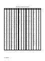
1
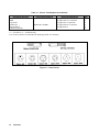
Keysight Model 66000A MPS Mainframe Service Guide CERTIFICATION Keysight Technologies certifies that this product met its published specifications at time of shipment from the factory. Keysight Technologies further certifies that its calibration measurements are traceable to the United States National Bureau of Standards, to the extent allowed by the Bureau's calibration facility, and to the calibration facilities of other International Standards Organization members. WARRANTY This Keysight Technologies hardware product is warranted against defects in material and workmanship for a period of three years from date of delivery. Keysight Technologies software and firmware products, which are designated by Keysight Technologies for use with a hardware product and when properly installed on that hardware product, are warranted not to fail to execute their programming instructions due to defects in material and workmanship for a period of 90 days from date of delivery. During the warranty period Keysight Technologies will, at its option, either repair or replace products which prove to be defective. Keysight Technologies does not warrant that the operation of the software, firmware, or hardware shall be uninterrupted or error free. For warranty service, with the exception of warranty options, this product must be returned to a service facility designated by Keysight Technologies. Customer shall prepay shipping charges by (and shall pay all duty and taxes) for products returned to Keysight Technologies for warranty service. Except for products returned to Customer from another country, Keysight Technologies shall pay for return of products to Customer. Warranty services outside the country of initial purchase are included in Keysight Technologies’ product price, only if Customer pays Keysight Technologies international prices (defined as destination local currency price, or U.S. or Geneva Export price). If Keysight Technologies is unable, within a reasonable time to repair or replace any product to condition as warranted, the Customer shall be entitled to a refund of the purchase price upon return of the product to Keysight Technologies. LIMITATION OF WARRANTY The foregoing warranty shall not apply to defects resulting from improper or inadequate maintenance by the Customer, Customer-supplied software or interfacing, unauthorized modification or misuse, operation outside of the environmental specifications for the product, or improper site preparation and maintenance. NO OTHER WARRANTY IS EXPRESSED OR IMPLIED. KEYSIGHT TECHNOLOGIES. SPECIFICALLY DISCLAIMS THE IMPLIED WARRANTIES OF MERCHANTABILITY AND FITNESS FOR A PARTICULAR PURPOSE. EXCLUSIVE REMEDIES THE REMEDIES PROVIDED HEREIN ARE THE CUSTOMER'S SOLE AND EXCLUSIVE REMEDIES. KEYSIGHT TECHNOLOGIES SHALL NOT BE LIABLE FOR ANY DIRECT, INDIRECT, SPECIAL, INCIDENTAL, OR CONSEQUENTIAL DAMAGES, WHETHER BASED ON CONTRACT, TORT, OR ANY OTHER LEGAL THEORY. ASSISTANCE The above statements apply only to the standard product warranty. Warranty options, extended support contracts, product maintenance agreements and customer assistance agreements are also available. Contact your nearest Keysight Technologies. Sales and Service office for further information on Keysight Technologies' full line of Support Programs. 2 SAFETY SUMMARY The following general safety precautions must be observed during all phases of operation of this mainframe. Failure to comply with these precautions or with specific warnings elsewhere in this guide violates safety standards of design, manufacture, and intended use of the mainframe. Keysight Technologies assumes no liability for the user's failure to comply with these requirements. GROUND THE MAINFRAME. This product is a Safety Class 1 instrument (provided with a protective earth terminal). To minimize shock hazard, the mainframe must be connected to an electrical ground. The mainframe must be connected to the ac power supply mains through a three-conductor power cable, with the third wire firmly connected to an electrical ground (safety ground) at the power outlet. Any interruption of the protective (grounding) conductor or disconnection of the protective earth terminal will cause a potential shock hazard that could result in personal injury. DO NOT EXCEED INPUT RATINGS. This mainframe is equipped with a power line filter to reduce electromagnetic interference and must be connected to a properly grounded receptacle to minimize electric shock hazard. Operation at line voltages or frequencies in excess of those stated on the line rating label may cause leakage currents in excess of 5.0 mA peak. DO NOT OPERATE IN AN EXPLOSIVE ATMOSPHERE. Do not operate the mainframe in the presence of flammable gases or fumes. BEFORE APPLYING POWER. Verify that the power cord is correctly connected to the mainframe. SAFETY SYMBOLS. Instruction manual symbol: the product will be marked with this symbol when it is necessary for the user to refer to the instruction manual (refer to Table of Contents) . Indicates hazardous voltages. Indicate earth (ground) terminal. The WARNING sign denotes a hazard. It calls attention to a procedure, practice, or the like, which, if not correctly performed or adhered to, could result in personal injury. Do not proceed beyond a WARNING sign until the indicated conditions are fully understood and met. The CAUTION sign denotes a hazard. It calls attention to an operating procedure, or the like, which, if not correctly performed or adhered to, could result in damage to or destruction of part or all of the product. Do not proceed beyond a CAUTION sign until the indicated conditions are fully understood and met. Mainframes that appear damaged or defective should be made inoperative and secured against unintended operation until they can be repaired by qualified service personnel. . 3 Printing History The current edition of this guide is indicated below. Reprints of this guide containing minor corrections and updates may have the same printing date. New editions are identified by a new printing date and, in some cases, by a new part number. A new edition incorporates all new or corrected material since the previous edition. Changes to the guide occurring between editions are covered by change sheets shipped with this guide. Edition 1 . . . November, 1992 Updated June, 2000 Updated April, 2001 Edition 2 . . . December, 2014 Copyright 1992, 2000, 2014 Keysight Technologies This document contains proprietary information protected by copyright. All rights are reserved. No part of this document may be photocopied, reproduced, or translated into another language without prior consent of Keysight Technologies. The information contained in this document is subject to change without notice. 4 Table of Contents Overview.................................................................................................................................................................................. 7 About This Manual ............................................................................................................................................................... 7 Related Documents ........................................................................................................................................................... 8 Revisions and Updates.......................................................................................................................................................... 8 Manual .............................................................................................................................................................................. 8 Firmware........................................................................................................................................................................... 8 Safety Considerations ........................................................................................................................................................... 8 Electrostatic Discharge ......................................................................................................................................................... 9 Service Tools and Equipment ............................................................................................................................................... 9 Verification............................................................................................................................................................................ 11 Preliminary Checkout ......................................................................................................................................................... 11 POWER-ON Checkout ....................................................................................................................................................... 12 Selftest Sequence ............................................................................................................................................................ 12 In Case of Trouble .......................................................................................................................................................... 12 Output Checkout ................................................................................................................................................................. 14 In Case of Trouble .......................................................................................................................................................... 14 Problem Not Identified ....................................................................................................................................................... 14 Disassembly ........................................................................................................................................................................... 15 Disassembly Procedures ..................................................................................................................................................... 15 Removing the Modules and Module Connectors ............................................................................................................ 15 Removing the Cover ....................................................................................................................................................... 15 Removing the Front Frame ............................................................................................................................................. 15 Removing the Front Bezels and Keyboard Plug ............................................................................................................. 16 Removing the Rear Subchassis ....................................................................................................................................... 16 Removing the Pc Boards................................................................................................................................................. 16 Reassembly Procedures ...................................................................................................................................................... 17 Installing the Pc Boards .................................................................................................................................................. 17 Assembling the Rear Subchassis..................................................................................................................................... 18 Assembling the Keyboard Plug and Front Bezels........................................................................................................... 18 Assembling the Front Frame ........................................................................................................................................... 18 Assembling the Cover ..................................................................................................................................................... 19 Troubleshooting .................................................................................................................................................................... 21 Troubleshooting Sequence.................................................................................................................................................. 21 Accessing the Flowcharts.................................................................................................................................................... 21 If You Experienced a Selftest Failure ............................................................................................................................. 21 If You Experienced Other Problems With the Mainframe.............................................................................................. 22 Troubleshooting Flowcharts ............................................................................................................................................... 22 Replacement Parts ................................................................................................................................................................ 33 Diagrams................................................................................................................................................................................ 39 Test Point and Component Location Diagram.................................................................................................................... 39 Main Board Schematics ...................................................................................................................................................... 39 Sheet 1 Circuit Functions................................................................................................................................................ 39 5 Sheet 2 Circuit Functions................................................................................................................................................ 39 Sheet 3 Circuit Functions................................................................................................................................................ 40 Backplane Board Schematic ............................................................................................................................................... 40 Exploded View Diagram..................................................................................................................................................... 40 Schematic Notes ................................................................................................................................................................. 41 Manual Backdating .............................................................................................................................................................. 49 Index ...................................................................................................................................................................................... 51 6 1 Overview About This Manual This manual is a complete guide for servicing the Keysight 66000A Modular Power System (MPS) Mainframe. Troubleshooting information for the Keysight 661xxA MPS Power Modules is provided in the module service manual (see "Related Documents"), which should be used with this manual. Note Troubleshooting the Keysight 66000A MPS Mainframe requires the use of one working Keysight 661xxA MPS Power Module. This manual is organized into the following major sections: Overview discusses safety and equipment considerations to be aware of when troubleshooting. It also lists the tools and equipment required for troubleshooting. Verification consists of a series of tests that are used to help isolate a fault. It includes the selftest sequence that runs automatically at power-on and verifies the integrity of the microprocessor, the GPIB and serial interfaces, and the memory. Disassembly procedures are used to disassemble the instrument for repair. Troubleshooting procedures systematically verify selected circuits to isolate the cause of a problem. Suggestions for remedying the problem are also provided. Troubleshooting procedures are provided for the following circuits: Bias Supplies. Microprocessor. RAM and ROM Memory. GPIB and Serial Interfaces. Discrete Fault Indicator/Remote Inhibit (DFI/RI) Circuitry. Trigger Circuits. Power Module Communication. Keyboard Accessory Port. Replacement Parts lists part numbers for electrical components and miscellaneous chassis parts. Schematics and component location diagrams are provided as an aid in troubleshooting and repair. Overview 7 Related Documents The following documents are related to this manual: Manual Keysight 66000A MPS Mainframe Installation Guide Keysight Series 661xxA MPS Power Modules User's Guide Keysight Series 661xxA MPS Power Modules Programming Guide Keysight Series 661xxA MPS Power Modules Service Manual Part Number Description 66000-90001 Provides product specifications, installation, and connection information. Describes the operation of the MPS Power Modules. Describes SCPI programming commands, status reporting. Provides replaceable-parts lists, circuit diagrams, and verification procedures for the Keysight Series 661xxA MPS Power Modules. 5959-3386 5959-3362 5959-3364 Revisions and Updates Manual Keysight Technologies instruments are identified by a 10-digit serial number. The format is described as follows: first two letters indicate the country of manufacture. The next four digits are a code that identify either the date of manufacture or of a significant design change. The last four digits are a sequential number assigned to each instrument. Item US 3648 0101 Description The first two letters indicates the country of manufacture, where US = USA; MY = Malaysia; SG = Singapore. This is a code that identifies either the date of manufacture or the date of a significant design change. The last four digits are a unique number assigned to each mainframe. If changes have been made to your unit since the publication of this manual, a yellow Manual Change sheet may be supplied with the manual. It defines the differences between your unit and the unit described in this manual. The yellow change sheet may also contain information for correcting errors in the manual. Note that because not all changes to the product require changes to the manual, there may be no update information required for your unit. Older serial number formats used with these instruments had a two-part serial number, i.e. 2701A-00101. This manual also applies to instruments with these older serial number formats. Refer to Manual Backdating for backdating information. Firmware This manual applies to mainframes that run on software revisions A.00.01 and up. The mainframe ROM chip has a label that specifies the firmware revision. Safety Considerations The Keysight 66000A MPS Mainframe is a Safety Class 1 instrument that has a protective earth terminal. Refer to the Safety Summary page at the beginning of this manual for general safety procedures and the meaning of safety symbols appearing in the manual and on the mainframe. 8 Overview Electrostatic Discharge The Modular Power System has components that can be damaged by ESD (electrostatic discharge). Failure to observe standard anti-static practices can result in serious degradation of performance even when complete failure does not occur. When working on the Modular Power System, observe all anti-static work practices. This includes, but is not limited to: Working at a static-free station, such as a table covered with static-dissipative laminate or with a conductive table mat (Keysight P/N 9300-0797). Using a conductive wrist strap (Keysight P/N 9300-0969 or 9300-0970). Grounding all metal equipment at the station to a single, common ground. Connecting low-impedance test equipment to static sensitive components only when those components have power applied to them. Removing power from the Modular Power System before removing or installing printed circuit boards. Service Tools and Equipment The following tools are required to repair the Keysight 66000A MPS Mainframe: T15 and T25 TORX drivers. 10mm and 7mm HEX NUT drivers. #2 POZI driver. Slot-head screwdrivers - small and medium. DIP component removal tool. Soldering iron and solder. De-solder removal tool. Needle-nose pliers. Anti-static work mat and wrist strap. The following equipment is required to troubleshoot the Keysight 66000A MPS Mainframe: Instrument Required Power Cords (see Figure 1-1) Test Cable Mini-Grapper clip leads DFI RI connector Table 1-1. Service Test Equipment Critical Specifications Recommended Model Option #831 P/N 8120-5573 Option #833 P/N 8120-5568 Option #834 P/N 8120-5566 Option #841 P/N 8120-5572 Option #843 P/N 8120-5571 Option #845 P/N 8120-5570 Option #846 P/N 8120-5565 Option #847 P/N 8120-5567 Option #848 P/N 8120-5569 BNC (male) to BNC (male) P/N 8120-1838 Wire Size: 24 AWG P/N 8120-3326 or 8120-3327 Type: Terminal Block 4-pos. P/N 1252-1488 (supplied with mainframe) 1 Use V,T V,T V,T V,T Overview 9 Table 1-1. Service Test Equipment (continued) Instrument Required MPS Power Module DMM Logic Probe Oscilloscope MPS Keyboard2 Isolation transformer Critical Specifications Bandwidth: 100 MHz Recommended Model Keysight 661xxA Series Keysight 34401A or equivalent Keysight 545A or equivalent Keysight 54504A or equivalent Keysight 66001A 1 V = Verification; T = Troubleshooting. 2 Use of the keyboard is recommended for displaying selftest error messages. Figure 1-1. Power Cords 10 Overview 1 Use V,T T T T V T 2 Verification Operation verification of the Keysight 66000A MPS Mainframe consists of performing the procedure that is located in this section. This procedure verifies that the mainframe is performing properly without testing all specified parameters. The tests include a preliminary checkout, power-on selftest, and module communication. Preliminary Checkout 1. Make sure that the front power switch is off (0). 2. Look at the "Line Rating" chart on the rear of the mainframe. a. Verify the modules are set to the appropriate line voltage setting. Line selector switches are located on the bottom of the modules. Note b. c. 3. At least one module is required to verify the operation of the mainframe. Remove the fuse and verify that the fuse is as specified on the label. Install the module(s). Make sure that the power cord is connected to the terminal block in accordance with the prevailing color code. Connection of this instrument to an ac power source should be done only by qualified personnel. Power Cord Wire Color Codes Label Line "L" Neutral "N" Ground UL/CSA Cords Black White Green or Green with Yellow stripe Harmonized Cordage Brown Blue Green with Yellow stripe 4. Make sure that there is no load connected to the output connector by removing the output connector assembly. 5. Verify that the GPIB address switch is set to the desired address (0 - 31). Verification 11 POWER-ON Checkout 1. Connect the instrument to the power source and turn the front power switch to ON (1). 2. Listen to confirm the modules' fans are on. The power supply undergoes a selftest when you turn it on. The power-on selftest sequence tests the microprocessor, GPIB interface, and serial communications. Selftest Sequence 3. All display digits and annunciators on the keyboard briefly turn on. 4. All front panel LEDs and annunciators on the modules briefly turn on. 5. The keyboard briefly displays the message: 6. The keyboard then displays the state of the addressed module. Note The information displayed on the keyboard assumes: At least one power module is installed, Factory default state still stored in location 0, Frame mode switch on the back of the mainframe is set to MAIN, GPIB address of the mainframe is set to 5, Module configuration switches set to factory default states (all OPEN). In Case of Trouble Note In case of a module failure, the front panel will display an Error Code -Uxx. Refer to the Keysight Series 661xxA Service Manual for information on troubleshooting the dc power modules. A problem exists in the mainframe when one of these conditions is observed during selftest: 12 Verification Table 2-1. Problem Symptoms Symptoms Probable Cause Troubleshooting Procedure Keyboard and modules remain turned off (fans not ON) Input Line Voltage, check fuse F8 Bias Troubleshooting Module fans turn ON, front displays remain blank (Turned OFF) No bias voltages, check fuses F1 & F2 Bias Troubleshooting Modules remain OFF, keyboard displays blinking cursor ¦ Primary Microprocessor (U44) defective, check fuse F1 ROM & Microprocessor Troubleshooting Keyboard displays Self-test Failed, ROM Checksum Test ROM (U51) defective ROM & Microprocessor Troubleshooting Keyboard displays Self-test Failed, Internal RAM Test Primary Microprocessor (U44) defective ROM & Microprocessor Troubleshooting Keyboard displays Self-test Failed, External RAM Test RAM (U52) defective ROM & Microprocessor Troubleshooting Keyboard displays Self-test Failed, GPIB Test GPIB Controller (U17) defective Overall Troubleshooting Keyboard displays Self-test Failed, Serial Comm Test DUART (U91) defective Overall Troubleshooting Keyboard displays NO MODULES INSTALLED Backplane power-up or communication defective Overall Troubleshooting2 Keyboard displays MODULE NOT FUNCTIONING Module defective or backplane communication defective Overall Troubleshooting 1 2 1 Refer to Chapter 4 of this manual for detailed troubleshooting procedures. Assumes that at least one module has been installed and is connected to the mainframe backplane. Verification 13 Output Checkout 1. Make sure that there is no load connected to the output connector by removing the output connector assembly. 2. Check the basic voltage functions and module communications as shown in following table: Action Keyboard Display Explanation 3. Press *RST Press :OUTP ON Press :CURR 1 Sets the output current to 1 A Press :VOLT 5 Sets the output voltage to 5 V Resets the Modular Power System Enables the output The keyboard display should now be in meter mode indicating the voltage and status of the dc power module: Disable the output prior to connecting a load. Press In Case of Trouble If the keyboard and module displays do not read the correct voltage, check the operation of the module. Refer to the "Performance Measurement" section of the Keysight Series 66lxxA Power Modules Service Manual. Problem Not Identified If after performing the checkout procedures you were unable to isolate the problem, refer to the "Overall Troubleshooting" procedure in Chapter 4. The overall troubleshooting procedure will verify whether the mainframe is at fault and will isolate the problem to a functional block. 14 Verification 3 Disassembly This chapter provides disassembly and reassembly instructions for the Keysight 66000A MPS Mainframe. Refer to Chapter 6 for an exploded view diagram of the mainframe. Major mechanical components are identified with "MP" designations and are referenced in this section. Refer to Chapter 5 for the component descriptions. Refer to Chapter 1 for the tools required to disassemble and reassemble the unit. Disassembly Procedures SHOCK HAZARD To avoid the possibility of personal injury, remove the mainframe from operation before removing the top cover. Turn off ac power and disconnect the line cord, GPIB cable, and load leads before attempting any disassembly. When servicing the Main assembly and Backplane assembly, ac line voltages are present on the Main board and backplane connectors. Most of the attaching hardware is metric. Use of other types of fasteners will damage threaded inserts. Removing the Modules and Module Connectors Before you can disassemble the mainframe, you must first remove all of the power supply modules as well as the module connectors on the back of the mainframe. 1. Use the slot-head screwdriver and release the pull tab at the front of each module. 2. Pull all of the modules out of the mainframe. 3. Use the Pozi driver and disconnect all of the module connectors from the back of the mainframe. Removing the Cover 1. Use the T25 driver and remove the four screws that attach the handles (MP22) to the chassis . 2. Slide the cover (MP6) back, spread the sides slightly, and lift the cover up. 3. Lift the top tray (MP3) out of the chassis. Removing the Front Frame The cover must be removed from the unit before you can remove the front frame. Disassembly 15 1. Use the T15 driver and remove the four screws that attach the front frame (MP18) to the chassis. 2. Slide the front frame forward about two inches. 3. Carefully unplug the cable (MP23) from the keyboard plug. Removing the Front Bezels and Keyboard Plug The front frame must be removed from the chassis before you can remove the bezel pieces (MP11-12). Note The keyboard plug (A3) can only be removed from the front frame after the bottom bezel (MP11) has been removed. 1. Insert the slot-head screwdriver into the notch at the bottom of each side bezel (MP12) to remove the bezels. 2. While applying upward pressure with the screwdriver to clear the latch, pull the side bezel away from the frame. When the latch clears the bottom bezel (MP11), the side bezel will come right out. 3. Repeat this procedure for the other side bezel. 4. When the side bezels have been removed, simply grasp the top (MP10) or bottom bezel (MP11) at either end and pull the bezels away from the frame. The bezels will snap out of the front frame. 5. Use the T15 driver to remove the two screws that attach the keyboard plug (A3). Removing the Rear Subchassis The cover must be removed from the unit before you can remove the rear subchassis (MP4). 1. Use the T15 driver and remove the six screws (three on each side) that attach the rear subchassis (MP4) to the chassis. 2. Slide the subchassis backward about three inches. 3. Carefully unplug the keyboard cable assembly (MP23) from the subchassis. 4. Grasp the on/off pushrod (MP13) firmly and unsnap it from the switch located inside the subchassis. Pull the pushrod straight back from the subchassis to unsnap it. 5. Remove the rear subchassis from the chassis. Removing the PC Boards The rear subchassis must be removed from the unit before you can remove the pc boards (A1, A2). Observe all standard anti-static procedures when removing the pc boards from the subchassis (see Chapter 1). 16 Disassembly 1. Use the Pozi driver and remove the line cord from the unit. Note the color code and location of each wire on the terminal block before removing the cord. 2. Use the T15 driver and remove the four screws (two on the front and two on the back) that attach the backplane cover (MP5) to the subchassis (MP4). 3. Pull the bottom edge of the cover out slightly so that it clears the alignment pins and lift the cover straight up. 4. Grasp the Backplane board (A2) firmly and lift it straight out of its plug-in sockets. 5. Check to make sure that the FLT/INH connector is unplugged from the back of the unit. 6. Use the 7mm hex driver and remove the two nuts that connect the GPIB connector to the rear panel. 7. Use the 10mm hex driver and remove the nut that connects the ground wire to the rear panel. 8. Use the T15 driver and remove the three screws that attach the Main board (A1) to the subchassis (MP4). 9. Carefully lift up the pc board and remove it from the subchassis. Reassembly Procedures Most of the attaching hardware is metric. Use of other types of fasteners will damage threaded inserts. Installing the PC Boards 1. Align the connectors on the Main board (A1) with the cutouts in the rear panel and carefully install the board in the subchassis (MP4). 2. Make sure the Main board is fully inserted in the notches along the edge of the subchassis. 3. Use the T15 driver and install the three screws that attach the Main board to the subchassis . 4. Use the 7mm hex driver and install the two flat washers, split washers, and nuts that fasten the GPIB connector to the rear panel. 5. Install the Backplane board (A2) into the connectors on the Main board. 6. Connect the ground hardware to the chassis in the following order: a. b. c. d. lock washer. ground wire. lock washer. nut. 7. Use the 10mm hex driver and tighten the grounding nut. 8. Align the slots in the backplane cover (MP5) with the notches on the Backplane board (A2) and snap the cover into place. Use the slot-head screwdriver to align the board in the slots. Disassembly 17 9. Make sure that the pins on the bottom of the cover are in their holes and that the cover is flush against the subchassis. 10. Use the T15 driver and install the four screws (two on the front and two on the back) that attach the backplane cover to the subchassis. Assembling the Rear Subchassis 1. Slide the rear subchassis (MP4) under the sides of the chassis but don't push it all the way in yet; leave about two inches of space. 2. Connect the keyboard cable (MP23) to the connector inside the subchassis. 3. Make sure that the on/off pushrod (MP13) and the chassis pins line up with the openings on the rear subchassis and slide the subchassis into place. 4. Use the T15 driver and install the six screws (three on each side) that attach the rear subchassis to the chassis. Don't tighten the screws until all six have been started. 5. Push the on/off pushrod (MP13) in from the front panel in until it snaps twice. The pushrod must snap twice to indicate that it is firmly connected to the switch inside the subchassis . Assembling the Keyboard Plug and Front Bezels 1. Use the T15 driver to install the two screws that attach the keyboard plug (A3) in the second and third hole on the bottom right corner of the front frame (MP18) when viewed from the front. The bottom of the frame is thicker than the top. 2. Align the pins on the top and bottom bezels (MP10, MP11) with the corresponding holes on the frame and snap the bezels into place. 3. Check along the edges of the top and bottom bezels to make sure that they are snapped all the way into place. 4. Install the side bezels (MP 12) by inserting the top corner of each bezel first, then push the bottom corner toward the side of the frame until it snaps into place. Assembling the Front Frame 1. Position the front frame (MP18) close to the front of the chassis. Insert the on/off pushrod (MP13) into its opening and connect the keyboard cable (MP23) to keyboard plug (A3). 2. Insert the sides of the chassis between the front frame (MP18) and the side bezels (MP12). Push the front frame onto the chassis as far it will go. 3. Use the T15 driver and install the four screws that attach the front frame to the chassis. 4. Look through the slots in the bottom tray and check that the keyboard cable (MP23) is positioned in the cable clamp. If not, insert the slot-head screwdriver through the slots in the bottom tray and slide the cable into the cable clamp. Don't force the tiewrap under the cable clamp; position the tiewrap in front of the cable clamp. 18 Disassembly Assembling the Cover 1. Place the top tray (MP3) on the chassis with the vents toward the front of the unit. 2. Spread the sides of the cover (MP6) and slide it onto the chassis so that it fits into the slot behind the front panel assembly. Check that the cover is flush against the rear panel. 3. Use the T25 driver and install the four screws that attach the handles and the cover to the chassis. 4. Reattach the line cord if it has been removed from the unit using the Pozi driver. If necessary, refer to the Mainframe Installation Guide for more information. Disassembly 19 4 Troubleshooting This chapter provides troubleshooting and repair information for the Keysight 66000A MPS Mainframe. Before attempting to troubleshoot the mainframe, ensure that the problem is not with an external circuit or application, an MPS Power Module, the GPIB controller, the application program, or the input power line. SHOCK HAZARD Most of the troubleshooting procedures given in this chapter are performed with power applied and protective covers removed. Such maintenance should be performed only by service trained personnel who are aware of the hazards (for example, fire and electrical shock). Troubleshooting Sequence 1. Verify that the Modular Power System mainframe is at fault. 2. Use the flowcharts to locate the mainframe functional block at fault. 3. Troubleshoot the functional block per flowchart instructions. Troubleshooting tests built into firmware are provided to isolate a problem to one of the circuit boards or to a particular circuit on the board. Once a problem has been isolated to a particular circuit, suggestions are given as to what component may be at fault. This instrument uses components that can be damaged or suffer serious performance degradation as a result of ESD (electrostatic discharge). Observe the standard anti-static precautions discussed in Chapter 1 to avoid damage to components. Accessing the Flowcharts If You Experienced a Selftest Failure If you experienced a selftest failure as described in Chapter 2, Table 2-1, disassemble the pc boards and proceed directly to the flowchart indicated in the "Troubleshooting Procedure" columns of Table 2-1. Figure 4-1 - Overall Troubleshooting. Figure 4-2 - Bias Troubleshooting. Figure 4-3 - ROM & Microprocessor Troubleshooting. Troubleshooting 21 If You Experienced Other Problems with the Mainframe If you experienced problems other than a selftest failure with the mainframe, proceed directly to Figure 4-1- Overall Troubleshooting. Troubleshooting Flowcharts The following troubleshooting flowcharts are provided to help you identify and isolate a problem to a specific circuit on the Main (Al) board. Once a problem has been narrowed down to a specific circuit, suggestions are provided as to the components that may be responsible for the problem. Refer to the schematic diagrams for detailed information on circuit wiring and component function. The overall troubleshooting flowchart (Figure 3-1) will identify most of the problems in the mainframe. The flowcharts of Figure 3-2 and Figure 3-3 will identify problems in the bias circuits and in the microprocessor circuits. To aid in troubleshooting, the GPIB address switch (S7) can be set to run various test routines as described in the flowchart. Placing a jumper on test header J5 is also required to configure and run certain tests. You must provide jumper clips for test header J5. Also, oscilloscope waveforms are provided on the flowchart along with the settings required to generate the waveforms. Connect the A1 board to ac mains through an isolation transformer when making measurements with an oscilloscope. The Backplane (A2) board contains no active components. The schematic diagram provides point-to-point wiring information of the connectors on the Backplane board. 22 Troubleshooting Figure 4-1. Overall Troubleshooting (Sheet 1 of 7) Troubleshooting 23 Figure 4-1. Overall Troubleshooting (Sheet 2 of 7) 24 Troubleshooting Figure 4-1. Overall Troubleshooting (Sheet 3 of 7) Troubleshooting 25 Figure 4-1. Overall Troubleshooting (Sheet 4 of 7) 26 Troubleshooting Figure 4-1. Overall Troubleshooting (Sheet 5 of 7) Troubleshooting 27 Figure 4-1. Overall Troubleshooting (Sheet 6 of 7) 28 Troubleshooting Figure 4-1. Overall Troubleshooting (Sheet 7 of 7) Troubleshooting 29 Figure 4-2. Bias Troubleshooting (Sheet 1 of 2) 30 Troubleshooting Figure 4-2. Bias Troubleshooting (Sheet 2 of 2) Troubleshooting 31 Figure 4-3. ROM & Microprocessor Troubleshooting 32 Troubleshooting 5 Replacement Parts Table 5-1 lists the electrical components and Table 5-2 lists the mechanical components for the Keysight 66000A MPS Mainframe. These tables provide the following information: Reference designation. Keysight Technologies part number. Description of part. You can order parts from your local Keysight Technologies sales office. A list of the regional sales offices is given at the back of this manual. When ordering parts, include the following information: Keysight Technologies part number. Description of the part. Quantity desired. MPS model number (Keysight 66000A). The test point and locations diagram in Chapter 6 identifies the location of the electrical components on the Main board. The exploded view diagram in Chapter 6 identifies some of the major mechanical components of the mainframe and how they are assembled. Parts with "MP" designations identify components that are referenced in the parts list. Replacement Parts 33 Table 5-1. Keysight 66000A MPS Mainframe Parts List - Electrical Reference Designators Part Number Al Cl,2 C3 C4 C5 C9-11 C12 C14 C15 C16 C17,18 C20 C42 C50-53 C56 C64 C65 C68 C85 C87 C88 C89 C90-92 C96 C98 C100,101 C102,103 C104 C106 C108 C110 C115 C116 C118 C123 C124 C125 C126,127 C133 C135,136 C137 C138,139 C140-143 C146 C150 C151 C160,161 66000-61020 0160-2025 0160-4808 0160-4835 0160-5534 0160-4822 0160-2025 0160-4787 0160-5422 0180-4136 0160-5422 0180-4405 0180-4136 0160-5422 0160-5422 0160-5422 0180-4136 0180-4136 0180-4396 0160-5422 0180-4136 0160-4807 0160-5422 0160-5422 0160-4807 0160-4822 0160-4807 0160-4835 0160-5422 0160-4281 0180-3805 0180-4394 0160-4831 0180-4395 0180-4405 0160-4830 0160-5469 0160-5422 0160-7606 0160-4281 0160-7606 0160-4183 0160-4822 0160-4835 0160-4830 0160-4822 0160-4439 34 Replacement Parts Description ASSEMBLY-MAIN BOARD CAPACITOR-FXD 220pF ±5% 500V CAPACITOR-FXD 470pF ±5% 100V CAPACITOR-FXD 0.1uF ±10% 50V CAPACITOR-FXD 0.1uF ±10% 63V CAPACITOR-FXD 1000pF ±5% 100V CAPACITOR-FXD 220pF ±5% 500V CAPACITOR-FXD 22pF ±5% 100V CAPACITOR-FXD 0.047uF ±20% 50V CAPACITOR-FXD 10uF ±10% 20V CAPACITOR-FXD 0.047uF ±20% 50V CAPACITOR-FXD 470uF ±20% 50V CAPACITOR-FXD 10uF ±10% 20V CAPACITOR-FXD 0.047uF ±20% 50V CAPACITOR-FXD 0.047uF ±20% 50V CAPACITOR-FXD 0.047uF ±20% 50V CAPACITOR-FXD 10uF ±10% 20V CAPACITOR-FXD 10uF ±10% 20V CAPACITOR-FXD 390uF ±20% 400V CAPACITOR-FXD 0.047uF ±20% 50V CAPACITOR-FXD 10uF ±10% 20V CAPACITOR-FXD 33pF ±5% 100V CAPACITOR-FXD 0.047uF ±20% 50V CAPACITOR-FXD 0.047uF ±20% 50V CAPACITOR-FXD 33pF ±5% 100V CAPACITOR-FXD 1000pF ±5% 100V CAPACITOR-FXD 33pF ±5% 100V CAPACITOR-FXD 0.1uF ±10% 50V CAPACITOR-FXD 0.047uF ±20% 50V CAPACITOR-FXD 2200pF ±20% 250V CAPACITOR-FXD 10uF ±20% 50V CAPACITOR-FXD 1000uF ±20% 40V CAPACITOR-FXD 4700pF ±10% 100V CAPACITOR-FXD 470uF ±20% 50V CAPACITOR-FXD 470uF ±20% 50V CAPACITOR-FXD 2200pF ±10% 100V CAPACITOR-FXD luF ±10% 50V CAPACITOR-FXD 0.047uF ±20% 50V CAPACITOR-FXD luF ±20% 250V CAPACITOR-FXD 2200pF ±20% 250V CAPACITOR-FXD luF ±20% 250V CAPACITOR-FXD 1000pF ±20% 250V CAPACITOR-FXD 1000pF ±5% 100V CAPACITOR-FXD 0.1uF ±10% 50V CAPACITOR-FXD 2200pF ±10% 100V CAPACITOR-FXD 1000pF ±5% 100V CAPACITOR-FXD 4700pF ±20% Table 5-1. Keysight 66000A MPS Mainframe Parts List - Electrical (continued) Reference Designators Part Number C162 C163 D26 D30-32 D34-40 D45 D46 D47,48 D49,50 D51,52 D56-58 Fl F2 F8 J1 J3 J5 J114 J116,117 J119 J120-122 J126 J200 L1 L2,3 L4 Q5,6 Q7 R1,2 R3 R4 R5 R6 R7 R9,10 R11 R12 R13 R14 R15 R16 R17 R18 R20,21 R35 R47 R88 0160-5422 1901-1087 1901-1087 1901-1098 1901-1214 1901-1128 1901-1130 66000-60003 1901-1098 1901-1098 2110-0688 2110-0699 2110-0655 1252-0268 1252-4307 1251-4926 1251-7330 1250-1842 1252-1014 1251-8667 1251-8675 66000-80004 66000-80003 06024-80094 66000-60002 0699-3196 0698-3155 0698-3136 0757-0465 0757-0463 0757-0273 0698-6348 0698-3155 0757-0394 0757-0459 0757-0407 0757-0280 0699-3419 0699-3420 0698-3628 0698-3155 0698-8827 0698-3155 0698-7933 Description CAPACITOR-FXD 0.047uF ±20% 50V NOT USED DIODE-POWER RECTIFIER 600V 3A 200ns DIODE-POWER RECTIFIER 600V 3A 200ns DIODE-SWITCHING lN4150 50V 200mA 4ns DIODE-POWER RECTIFIER 600V lA 50ns DIODE-SCHOTTKY 40V lA DIODE-GENERAL PURPOSE 600V 8A 50ns TO-220AC DIODE-WITH HEATSINK ASSEMBLY DIODE-SWITCHING lN4150 50V 200mA 4ns DIODE-SWITCHING lN4150 50V 200mA 4ns FUSE-SUBMINIATURE 3A 125V NTD AX UL CSA FUSE-SUBMINIATURE 5A 125V NTD AX UL CSA FUSE (METRIC) 3.15A 250V NTD FE IEC CONNECTOR-RECT MICRORBN 24-CKT 24-CONTACT CONNECTOR-UTIL P-&-SKT 4-CKT 4-CONTACT CONNECTOR-POST TYPE .100-PIN-SPCG 8-CONTACT MODULAR PHONE RECEPTACLE RIGHT ANGLE PC MOUNT CONNECTOR-RF BNC FEM PC-W-STANDOFFS 50-OHM CONNECTOR-RECT SDL 6-CKT 6-CONTACT CONNECTOR-POST TYPE .100-PIN-SPACING 20-CONTACT CONNECTOR-POST TYPE .100-PIN-SPACING 5-CONTACT NOT USED CHOKE - INPUT CHOKE- OUTPUT CHOKE - RFI TRANSISTOR, FET WITH HEATSINK ASSEMBLY NOT USED RESISTOR 150 ±5% 10W RESISTOR 4.64K ±1% .125W RESISTOR 17.8K ±1% .125W RESISTOR 100K ±1% .125W RESISTOR 82.5K ±1% .125W RESISTOR 3.01K ±1% .125W RESISTOR 3K ±0.1% .125W RESISTOR 4.64K ±1% .125W RESISTOR 51.1 ±1% .125W RESISTOR 56.2K ±1% .125W RESISTOR 200 ±1% .125W RESISTOR 1K ±1% .125W RESISTOR RESISTOR RESISTOR 220 ±5% 2W RESISTOR 4.64K ±1% .125W RESISTOR 1M ±1% .125W TF RESISTOR 4.64K ±1% .125W RESISTOR 3.83K ±0.1% .125W Replacement Parts 35 Table 5-1. Keysight 66000A MPS Mainframe Parts List - Electrical (continued) Reference Designators Part Number R89 R93 R95 R98 R99 R100 R101 R102,103 R106 R107,108 R109 R110 R113 R114,115 R121 R130 R131-133 R146 R147 R149 R152-154 R157 R160-164 R165 R166,167 R168,169 R172 R174-175 R180,181 R182 R184 R185 R186,188 R187 SCKTl SCKT2 SCKT3 SCKT4 S2 S7 TB2 TB5 T1 T2 T3 U1 U2 0698-6348 0698-3625 0698-3439 0698-4037 0698-3155 0698-4037 0698-3155 0698-4037 1810-0206 0757-0442 0698-0082 0757-0442 0683-1015 1810-0305 0757-0394 0698-3609 0757-0394 0757-0442 0698-0082 0757-0428 0683-1015 0698-3155 0698-8812 0757-0442 0698-3155 0811-1848 0698-8827 0757-0398 0698-3433 0686-2705 0698-3155 0698-0082 0686-2705 1200-1274 1200-0485 1200-0567 1200-0639 3101-2808 3101-2097 0360-2312 0360-2421 9100-4933 66000-80001 66000-80002 1826-2056 1990-1502 36 Replacement Parts Description RESISTOR 3K ±0.1% .125W RESISTOR 160 ±5% 2W RESISTOR 178 ±1% .125W RESISTOR 46.4 ±1% .125W RESISTOR 4.64K ±1% .125W RESISTOR 46.4 ±1% .125W RESISTOR 4.64K ±1% .125W RESISTOR 46.4 ±1% .125W NETWORK-RESISTOR 8-SIP 10.0K OHM X 7 RESISTOR 10K ±1% .125W RESISTOR 464 ±1% .125W RESISTOR 10K ±1% .125W RESISTOR 100 ±5% .25W NETWORK-RESISTOR 9-SIP 4.7K OHM X 8 RESISTOR 51.1 ±1% .125W RESISTOR 22 ±5% 2W RESISTOR 51.1 ±1% .125W RESISTOR 10K ±1% .125W RESISTOR 464 ±1% .125W RESISTOR 1.62K ±1% .125W RESISTOR 100 ±5% .25W RESISTOR 4.64K ±1% .125W RESISTOR 1 ±1% .125W RESISTOR 10K ±1% .125W RESISTOR 4.64K ±1% .125W RESISTOR .5 ±10% 5W RESISTOR 1M ±1% .125W TF RESISTOR 75 ±1% .125W RESISTOR 28.7 ±1% .1 25W RESISTOR 27 ±5% 0.5W RESISTOR 4.64K ±1% .125W RESISTOR 464 ±1% .125W NOT USED RESISTOR 27 ±5% 0.5W SOCKET-IC-CHIP-CARRIER 68-CONTACT (REF U44) SOCKET-IC-DIP 14-CONTACT (REF S7) SOCKET-IC-DIP 28-CONTACT (REF U51) SOCKET-IC-DIP 20-CONTACT (REF U58,U66) SWITCH-PB DPST 4A 250Vac SWITCH-DIP SL 6-lA 0.1A 50Vdc TERMINAL BLOCK 4-TERMINAL .039 IN SQUARE TERMINAL BLOCK 3-TERMINAL RT-ANGLE 5-POSITION TRANSFORMER-FLYBACK FREQ: 100KHz TRANSFORMER-BIAS TRANSFORMER-DRIVER IC V REGULATOR-SWG 4.9/5.1V 8-DIP-P IC OPTO-ISOLATOR Table 5-1. Keysight 66000A MPS Mainframe Parts List - Electrical (continued) Reference Designators Part Number U4 U17 U44 U50 U51 U52 U58 U64 U66 U68 U71,72 U74 U80 U87 U89 U91 U97 U98 U99 VR4 VR11,12 VR13 VR14,15 VR16 VR17 VR53 Y1 1826-1343 1821-1740 1821-1479 1820-2724 66000-80016 1818-4134 66000-80010 1990-0543 66000-80017 1826-2341 1820-3176 1820-3206 1820-3097 1820-3206 1820-6789 1821-4383 1820-3176 1820-6045 1820-6170 1902-0244 1902-0953 1902-0959 1902-0953 A2 J1-8 J9-11 J12 66000-61021 1251-8414 1251-8666 1252-4306 ASSEMBLY-BACKPLANE BOARD CONNECTOR-POST TYPE .100-PIN-SPACING 48-CONTACT CONNECTOR-POST TYPE .100-PIN-SPACING 20-CONTACT CONNECTOR-UTIL P-&-SKT 4-CKT 4-CONTACT A3 J301 J302 66000-61022 1252-1014 1251-8608 ASSEMBLY-KEYBOARD CONNECTOR BOARD CONNECTOR-RECT SDL 6-CKT 6-CONTACT CONNECTOR-POST TYPE .100-PIN-SPACING 5-CONTACT 1902-0244 1902-0766 0410-2109 Description IC V REGULATOR-V-REFERENCE-ADJ 2.5/36V 8-DIP-P IC-GPIB TALKER/LISTENER IC-16-BIT MICROPROCESSOR, I/O, TIMER, TIMER, A/D IC LATCH TTL/ALS TRANSPARENT OCTL IC ROM GPIB - PROGRAMMED IC 64K SRAM 35-NS CMOS IC PROGRAMMABLE-LOGIC CMOS EEPLD - PROGRAMMED IC OPTO-ISOLATOR LED-PXSTR IF=150MA-MAX IC GAL DECODER - PROGRAMMED IC V REGULATOR-SWG 8-DIP-P IC MULTIPLEXER/DATA-SELECT CMOS/HC 8-TO-l-LINE IC LATCH CMOS/HC ADDRESSABLE POS-EDGE-TRIG IC GATE CMOS/HC AND QUAD 2-INPUT IC LATCH CMOS/HC ADDRESSABLE POS-EDGE-TRIG IC INTERFACE TRANSCEIVER IC DUAL UART, 68000 COMPATIBLE IC MULTIPLEXER/DATA-SELECT CMOS/HC 8-TO-l-LINE IC-GPIB TRANSCEIVER CHIP IC-GPIB TRANSCEIVER CHIP DIODE-ZENER 30V 5% 1W DIODE-ZENER 6.2V 5% DO-35 PD=.4W DIODE-ZENER 11V 5% DO-35 PD=.4W DIODE-ZENER 6.2V 5% DO-35 PD=.4W NOT USED DIODE-ZENER 30V 5% DIODE-ZENER 18.2V 5% DO-35 PD=.4W CRYSTAL-QUARTZ 12.00MHz Replacement Parts 37 Table 5-2. Keysight 66000A MPS Mainframe Parts List - Mechanical Ref. Des MP1 MP2 MP3 MP4 MP6 MP10 MP11 MP12 MP13 MP14 MP15 MP16 MP17 MP18 MP19 MP20 MP21 MP22 MP23 MP24 MP25 (Jl) (Jl) (Jl) (Jl) (L2,3) (L4) (F8) (TB2) (TB5) Qty Part Number Description 1 1 1 1 1 1 1 2 1 8 1 2 1 1 4 2 2 2 1 1 1 2 2 2 2 2 1 1 1 2 18 4 2 66000-00001 66000-00002 66000-00003 5001-9840 66000-00007 66000 40002 66000-40003 66000-40004 66000-40005 66000-40006 5041-8802 5001-0540 66000-80007 5021-8405 5041-8801 5041-8819 5041-8820 5062-3705 66000-80008 8160-0728 5040-1676 0380-0644 2190-0034 2190-0849 0515-0406 0380-0625 1480-0552 2110-0714 1252-1488 0515-1146 0515-0380 0515-1384 0515-2086 66000-60051 0535-0038 2190-0084 0403-0267 1400-1195 1400-0308 5080-2148 66000-80006 66000-90001 66001-90001 66001-90003 5040-1697 CHASSIS- MAIN CHASSIS TRAY - BOTTOM CHASSIS TRAY - TOP SUBCHASSIS COVER - UNIT BEZEL - TOP BEZEL- BOTTOM BEZEL- SIDE PUSHROD - ON/OFF PANEL - FILLER TRIM - TOP TRIM - SIDE NAMEPLATE FRAME - FRONT FOOT CAP - STRAP HANDLE (FRONT) CAP - STRAP HANDLE (REAR) STRAP HANDLE ASSEMBLY- KEYBOARD CABLE RFI STRIP AC INPUT SAFETY COVER (WITH HARDWARE) STANDOFF - HEX .255-IN-LG 6-32-THD WASHER - LOCK HLCL WASHER- FLAT MTLC SCREW - MACHINE M3 X 0.5 8MM-LG (Jl TO PC BOARD) STANDOFF - ROUND .687-IN-LG PIN - ESCUTCHEON .095-IN-DIA 2.09-IN-LG STL FUSEHOLDER TERMINAL BLOCK 4-POSITION SCREW - MACHINE M3 X 0.5 6MM-LG (TB5 TO PC BOARD) SCREW - MACHINE M4 X 0.7 10MM-LG (CHASSIS HARDWARE) SCREW - MACHINE M5 X 0.810MM-LG (HANDLE HARDWARE) SCREW - SPCL M4 X 0.7 7MM-LG (A3 TO FRONT FRAME) ASSEMBLY- SAFETY GROUND WIRE NUT - HEX DBL-CHAM M6 X 1.0 5.7MM-THK (SAFETY GROUND) WASHER - LOCK INTL T 1/4 IN .256 IN-ID (SAFETY GROUND) BUMPER FOOT-ADHESIVE MOUNTING CLAMP .38-DIA l-WD NYLON (KEYBOARD CABLE) TIE WRAP (KEYBOARD CABLE) CABLE - SERIAL LINK (2 METER) LABEL - REAR PANEL MANUAL - MPS USER'S GUIDE MANUAL - QUICK REFERENCE GUIDE INSTRUCTION SHEET - KEYBOARD INSTALLATION BLOCK-TOP COVER 2 2 2 2 38 Replacement Parts 6 Diagrams This chapter contains a test point and component location diagram and schematics for troubleshooting the Keysight 66000A MPS Mainframe. An exploded view diagram of the mechanical parts is also provided. Test Point and Component Location Diagram The test point and component location diagram identifies the location of the test points that are used in the troubleshooting procedures of Chapter 4, and are also shown on the schematic diagrams. The test point and locations diagram also identifies all electrical components on the Main board. The diagram is divided into columns and rows designated "x coordinates" and "y coordinates". The accompanying table lists all of the components on the Main board and gives the coordinate location of each component. For example, resistor R154 is located at x coordinate 12.3 and y coordinate 3.3. Refer to Chapter 5 for the part number and description of each electrical part. Main Board Schematics SHOCK HAZARD When servicing the Main assembly and Backplane assembly, ac line voltages are present on the Main board and backplane connectors. Three foldout sheets comprise the Main board schematic diagrams. The circuit functions of each schematic sheet are given as follows: Sheet 1 Circuit Functions Among the circuit components included on Sheet 1 are: microprocessor U44, GPIB interface chips U15 and U17, ROM chip U51, RAM chip U52, keyboard input J119 and J126, serial link input/output J114, and address switch S7. The GPIB interface is the link between the mainframe and the system controller. The keyboard input is the link between the mainframe and the Keysight 66001A keyboard. All communication between the mainframe and the controller or keyboard is processed by U44. Data communication between the modules and the controller is also directed through U44. Switch S7 determines the address of the mainframe. It also indicates if the mainframe is directly connected to the GPIB, or linked to another mainframe. During troubleshooting, switch S7 is used to select diagnostic tests for troubleshooting. Pins on test header J5 must be jumpered to perform certain diagnostic tests. Sheet 2 Circuit Functions Among the circuits included on Sheet 1 are: rectifier diodes D26, D30-D32, filter capacitor C85, FET switches Q5 and Q6, power transformer T1, bias transformer F2, FET pulse control chip U1, and pulse transformer T3. Isolation between the ac input and the digital circuit is provided by T1 and opto-isolator U2. Diagrams 39 Power to the mainframe is provided by a switching power supply. Energy is stored in the magnetic field of transformer T1 when current flows in the primary, and is transferred to the secondary side when the current flow in the primary is turned off. Primary current flow is controlled by FET switches, which are turned on and off at an 85KHz rate by U1. Regulation is accomplished by controlling the on-time of the FET switches. U1 monitors the voltage at the secondary side of T1 through opto-isolator U2 and adjusts the on-time of the FETs accordingly. T2 provides bias power for U1. Power at the secondary side of T1 is rectified and filtered to provide +5V power to the mainframe and +5V and +28V power to the turn-on circuits in the modules. Sheet 3 Circuit Functions Among the circuit components included on Sheet 1 are: multiplexers U71 and U72, demultiplexers U74 and U87, power-on chip U68, Trigger In/Out BNC connectors J116 and J117, and DFI/RI connector TB2. The multiplexers and demultiplexers direct the digital signals from the microprocessor and distribute them among the eight module slot locations via J121 and J122. +5V and +28V bias power is distributed to the module slot locations via J120. U68 generates a power-on (power is available) signal to the module slot locations via J120. Note J120 connects to J10 on the Backplane board, J121 connects to J9 on the Backplane board, and J122 connects to J11 on the Backplane board. The Trig IN signal from J117 is distributed to the module slot locations via J120. The Trig OUT signal to J116 is directly received from the module slot locations via J120. The RI (remote inhibit) signal from TB2 is processed by U44. U44 also generates the DFI (discreet fault indicator), which is connected to TB2 via opto-isolator U64. Backplane Board Schematic SHOCK HAZARD When servicing the Main assembly and Backplane assembly, ac line voltages are present on the Main board and backplane connectors. The Backplane board schematic shows the distribution of the ac power and control signals from the Main board to the eight module connectors. There are no active components on the Backplane board. Exploded View Diagram The exploded view diagram at the end of this section documents how the major components of the Keysight 66000A MPS Mainframe are assembled. Parts with "MP" designations identify components that are referenced in the parts list. Refer to Chapter 5 for the part number and description of the mechanical parts. 40 Diagrams Schematic Notes Notes that apply to all schematic sheets are given as follows: All resistors are in ohms 1%, 1/8W, unless otherwise specified. All capacitors are in microfarads unless otherwise specified. An asterisk negates a signal name. For example, WR appears on the schematic as WR*. Signal line destinations are given inside the parentheses at the end of the signal lines. For example, RDY (S0lA5), indicates that the RDY signal continues on schematic sheet 01 at grid coordinates A, 5. Coordinates are labeled on the schematic border. Signal lines that are terminated by flags continue onto other sheets. Note that flags do NOT indicate signal flow direction. Signal lines without flags go to another location of the same schematic sheet. Test points on the schematic sheets (e.g. TP3) identify the location of the test points used in the troubleshooting procedures in Chapter 4. Voltages and waveforms shown on the schematics are obtained when following the troubleshooting procedures in Chapter 4. Diagrams 41 Main Board Component Coordinates C1 C2 C3 C4 C5 C9 C10 C11 C12 C14 C15 C16 C17 C18 C20 C42 C50 C51 C52 C53 C56 C64 C65 C68 C85 C87 C88 C89 C90 C91 C92 C96 C98 C100 C101 C102 C103 C104 C106 C108 C110 C115 C116 C118 C123 X 5.2 6.7 3.8 4.0 5.0 3.9 14.8 14.3 6.2 3.3 3.6 15.0 14.9 14.8 8.3 13.7 10.9 11.1 11.0 13.8 9.6 11.0 11.1 10.9 3.5 14.4 14.7 12.7 9.7 8.6 8.6 8.1 12.8 10.5 11.0 10.3 11.2 13.0 13.3 2.7 4.2 7.4 6.6 7.5 7.9 42 Diagrams Y 2.9 3.5 3.4 3.9 4.1 3.9 3.5 3.5 0.5 3.9 3.4 1.0 3.5 1.0 0.6 2.4 1.5 0.9 2.3 3.1 1.6 3.0 1.5 3.0 2.2 0.7 1.0 0.5 0.9 3.1 2.2 3.8 0.5 3.3 3.3 4.4 3.8 2.4 3.8 2.3 4.4 2.2 1.2 0.7 2.7 C124 C125 C126 C127 C133 C135 C136 C137 C138 C139 C140 C141 C142 C143 C146 C150 C151 C160 C161 C162 C163 D26 D30 D31 D32 D34 D35 D36 D37 D38 D39 D40 D45 D46 D47 D48 D49 D50 D51 D52 D56 D57 D58 Fl F2 X 5.4 5.6 14.1 12.5 0.2 2.5 2.3 2.8 1.6 2.3 10.8 14.3 11.0 10.7 12.9 12.2 10.4 0.6 0.6 15.0 14.8 4.2 3.6 3.6 3.7 13.6 12.9 13.5 12.8 12.7 13.2 13.1 4.5 5.3 5.8 4.9 6.5 6.7 6.3 5.1 12.8 13.8 13.7 8.5 14.8 Y 0.4 0.5 4.0 3.3 3.0 2.3 1.8 3.0 4.2 4.2 1.8 1.2 0.9 1.2 2.4 3.9 3.8 2.0 1.8 3.5 2.5 1.3 1.4 1.1 0.7 3.8 3.8 3.8 3.1 3.1 3.1 3.1 3.9 4.4 2.6 2.6 1.5 1.2 3.8 3.8 3.8 3.8 3.8 3.1 2.7 F8 HS10 HS11 HS12 HS13 Jl J3 J5 J114 J116 J117 J119 J120 J121 J122 J126 J200 L1 L2 L3 L4 MC1 Q5 Q6 Q7 R1 R2 R3 R4 R5 R6 R7 R9 R10 R11 R12 R13 R14 R15 R16 R17 R18 R20 R21 R35 X 0.4 4.8 6.5 6.4 6.8 8.6 3.5 14.3 11.1 12.6 13.6 14.1 10.4 8.5 4.7 15.0 14.8 1.5 8.1 7.4 1.4 8.5 6.4 4.9 14.3 4.5 7.3 13.9 3.7 3.4 3.5 4.0 5.2 5.1 10.9 4.5 4.6 3.9 5.2 7.1 3.6 6.7 14.7 14.4 0.6 Y 2.8 3.7 3.7 1.6 1.1 4.2 0.0 1.7 4.3 3.9 3.9 4.3 0.0 0.0 0.0 0.3 2.0 3.1 1.7 1.5 1.3 3.4 3.7 3.7 2.5 2.4 2.9 2.4 3.4 3.9 3.4 3.4 0.9 0.4 0.4 0.9 3.9 3.4 4.4 1.2 3.1 0.7 4.0 4.0 3.5 R47 R88 R89 R93 R95 R98 R99 R100 R101 R102 R103 R106 R107 R108 R109 R110 R113 R114 R115 R121 R130 R131 R132 R133 R146 R147 R149 R152 R153 R154 R157 R160 R161 R162 R163 R164 R165 R166 R167 R168 R169 R172 R180 R181 R182 X 14.1 12.7 12.8 13.1 11.3 10.7 10.6 10.9 10.8 12.9 13.0 7.1 12.4 14.0 13.9 14.2 12.7 8.7 8.6 5.3 6.2 6.3 6.8 5.2 11.4 12.6 5.8 14.6 14.5 12.3 14.7 6.3 6.4 6.5 6.6 6.7 10.9 14.3 14.2 2.9 3.0 12.1 1.1 1.6 2.4 Y 2.4 2.4 1.9 4.1 3.3 3.3 3.8 3.3 3.3 2.6 3.1 3.8 3.3 4.0 3.8 3.5 3.3 0.9 1.5 3.3 2.0 3.9 3.9 3.3 3.3 3.3 0.4 4.0 4.0 3.3 2.7 2.9 2.9 2.9 2.9 2.9 2.3 2.4 2.4 1.1 0.7 3.8 2.0 2.1 2.8 R184 R185 R186 R187 R188 S2 S7 T1 T2 T3 TB2 TB5 U1 U15 U17 U2 U4 U44 U50 U51 U52 U58 U64 U66 U68 U71 U72 U74 U80 U87 U89 U91 U97 VR11 VR12 VR13 VR14 VR15 VR16 VR53 Y1 X 8.5 9.7 14.4 2.4 2.4 1.0 7.1 4.8 5.5 5.5 12.0 1.4 3.4 8.3 8.8 3.9 4.6 13.6 11.3 11.2 11.2 9.9 11.6 11.3 13.2 8.7 8.8 9.9 13.9 9.9 13.3 8.8 7.1 13.4 10.4 11.1 14.0 10.3 14.5 12.2 13.4 Y 2.3 1.1 2.4 2.6 2.7 1.5 3.9 1.0 3.4 4.3 4.3 4.3 4.0 3.2 2.5 0.5 0.4 0.7 0.4 2.5 2.0 1.3 3.5 1.0 2.0 1.0 0.4 0.9 2.8 0.4 2.7 1.7 3.4 3.8 4.4 3.8 2.4 3.8 2.4 3.8 0.5 TP 1 TP13 TP14 COM TP 3 TP 7 TP 6 TP 8 TP11 TP 9 TP 5 TP 4 TP10 TP 2 TP12 TP 0 Manual Backdating This section describes changes that must be made to the manual so that it applies to mainframes with older serial number formats. Look in the following table for the serial number of your instrument, and make only those changes listed for your instrument. Note that for some changes, you may be instructed to update the instrument if certain components are being replaced during repair. Serial Prefix 3302A 3350A 3445A 3445A 3522A 66000A Serial Number 00101-00835 00836-00945 00946-01255 01256-01560 01561-03295 US35220101-MY400000306 Changes 1-5 1-4 1-3 1, 2 1 1 Change 1 In Table 5-1 and on the schematic, Delete: R174, R175, and VR17. Change U17 to p/n 1820-2549. Change U51 to p/n 66000-80009. Change U66 to p/n 66000-80011. Change 2 Make the following changes in Table 5-2: Change: MP4 from a single subchassis (p/n 5001-9840) to two subchassis parts: MP4 (p/n 66000-00004) and MP5 (p/n 66000-00006). Change: Screw (p/n 0515-0380) from qty 18 to qty 20 Delete: Cover block, p/n 5040-1697 Change 3 In Table 5-1 and on the schematic, delete VR4, p/n 19020244. In its place add C4, 0.1uF, 50V p/n 0160-4835. Change 4 In Table 5-1 and on the schematic, delete U98 (18206045) and U99 (1820-0244). In their place add a single IC assembly, U15, p/n 1LH4-0001. Change 5 In Table 5-1 and on the schematic change R182 and R187 to 42.2 ohms p/n 0757-0316. Add R188, 42.2 ohms p/n 0757-0316 in parallel with R182 and R187. Manual Backdating 49 Index 2 +28V............................................................................................................................................................................ 31 5 +5V.............................................................................................................................................................................. 30 A ACON.......................................................................................................................................................................... 25 "ACON/MOD ID Test" ............................................................................................................................................... 25 ACONWR ................................................................................................................................................................... 25 "Address/Data Bus Test" ............................................................................................................................................. 23 address lines ................................................................................................................................................................ 32 ALE ............................................................................................................................................................................. 32 B Backplane Power-up Test ............................................................................................................................................ 25 "Backplane Serial Port Test" ....................................................................................................................................... 25 bias voltages .......................................................................................................................................................... 23, 30 BPCLR* ...................................................................................................................................................................... 31 C checkout ...................................................................................................................................................................... 11 D data lines...................................................................................................................................................................... 32 DFIB* .......................................................................................................................................................................... 27 "DFI/RI Pulse Train Test" ........................................................................................................................................... 27 DFI/RI Test Connector ................................................................................................................................................ 26 disassembly cover ..................................................................................................................................................................... 15 front frame ............................................................................................................................................................ 15 modules ................................................................................................................................................................ 15 pc board ................................................................................................................................................................ 16 subchassis ............................................................................................................................................................. 16 documents - related........................................................................................................................................................ 8 E electrical parts ............................................................................................................................................................. 34 electrostatic discharge ................................................................................................................................................... 9 equipment ...................................................................................................................................................................... 9 error code .................................................................................................................................................................... 12 Index 51 F fuse .............................................................................................................................................................................. 11 fuse F1 ......................................................................................................................................................................... 30 fuse F2 ......................................................................................................................................................................... 31 G "GPIB Switch Test"..................................................................................................................................................... 24 H HSRQ .......................................................................................................................................................................... 26 K keyboard ................................................................................................................................................................ 10, 12 Keyboard Display Test ................................................................................................................................................ 29 Keyboard Echo Test .................................................................................................................................................... 29 L line voltage .................................................................................................................................................................. 11 M mechanical parts .......................................................................................................................................................... 38 microprocessor ............................................................................................................................................................ 32 MODID ....................................................................................................................................................................... 25 O output checkout ........................................................................................................................................................... 13 overall troubleshooting ................................................................................................................................................ 23 P PCLR* ......................................................................................................................................................................... 31 power cord ............................................................................................................................................................. 10, 11 power module ................................................................................................................................................................ 7 "PSRQ Pulse Train Test" ............................................................................................................................................ 26 R RD .............................................................................................................................................................................. 32 reassembly ................................................................................................................................................................... 17 revision number ............................................................................................................................................................. 8 RIB .............................................................................................................................................................................. 27 ROM ............................................................................................................................................................................ 32 RXF ............................................................................................................................................................................. 26 RXKB .......................................................................................................................................................................... 23 52 Index S SACLK ...................................................................................................................................................... 23, 24, 25, 27 SASTRT .............................................................................................................................................. 24, 25, 26, 27, 28 schematic notes ..................................................................................................................................................................... 41 schematics ................................................................................................................................................................... 39 backplane board ................................................................................................................................................... 40 main board ............................................................................................................................................................ 39 selftest.......................................................................................................................................................................... 12 "Serial Link Test" ........................................................................................................................................................ 28 serial number ................................................................................................................................................................. 8 service manual ............................................................................................................................................................... 8 shock hazard .......................................................................................................................................................... 21, 39 T TINF ............................................................................................................................................................................ 28 tools ............................................................................................................................................................................... 9 TP0 .............................................................................................................................................................................. 23 TP1 ........................................................................................................................................................................ 23, 30 TP2 .................................................................................................................................................................. 23, 30, 31 TP4 .................................................................................................................................................................. 23, 30, 31 TP5 ........................................................................................................................................................................ 30, 31 TP6 .............................................................................................................................................................................. 32 TP7 .............................................................................................................................................................................. 32 TP8 .............................................................................................................................................................................. 32 "TrigIn/TrigOut Test" ................................................................................................................................................. 27 troubleshooting ............................................................................................................................................................ 21 flowcharts ............................................................................................................................................................. 22 TXF ............................................................................................................................................................................. 26 TXFEN ........................................................................................................................................................................ 26 TXKB .......................................................................................................................................................................... 23 W WR* ............................................................................................................................................................................ 32 Index 53 This information is subject to change without notice. © Keysight Technologies 1992, 2000, 2014 Edition 2, December 2014 66000-90003 www.keysight.com 54 Index