1
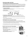
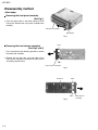
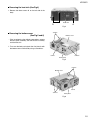
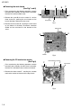
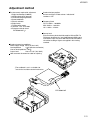
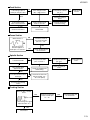
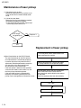
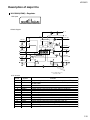
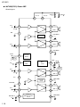
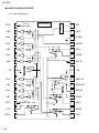
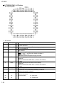
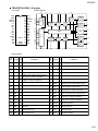
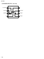
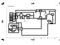
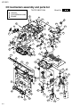
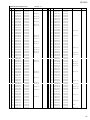
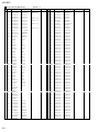
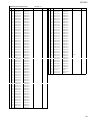
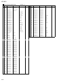
KD-S621
SERVICE MANUAL
CD RECEIVER
KD-S621
FM
LOUD
CD
SEL
¢
SSM
4
AM
DISP
7
8 MO
9
10
11 RPT
12 RND
MODE
SCM
Area Suffix
E -------- Continental Europe
EX ------------ Central Europe
Contents
Safety precaution
Preventing static electricity
Disassembly method
Adjustment method
COPYRIGHT
1-2
1-3
1-4
1-11
Flow of functional
operation unit TOC read
Maintenance of laser pickup
Replacement of laser pickup
Description of major ICs
2002 VICTOR COMPANY OF JAPAN, LTD.
1-12
1-14
1-14
1-15 26
No.49675
Jan. 2002
KD-S621
Preventing static electricity
1.Grounding to prevent damage by static electricity
Electrostatic discharge (ESD), which occurs when static electricity stored in the body, fabric, etc. is discharged,
can destroy the laser diode in the traverse unit (optical pickup). Take care to prevent this when performing repairs.
2.About the earth processing for the destruction prevention by static electricity
Static electricity in the work area can destroy the optical pickup (laser diode) in devices such as CD players.
Be careful to use proper grounding in the area where repairs are being performed.
2-1 Ground the workbench
Ground the workbench by laying conductive material (such as a conductive sheet) or an iron plate over
it before placing the traverse unit (optical pickup) on it.
2-2 Ground yourself
Use an anti-static wrist strap to release any static electricity built up in your body.
(caption)
Anti-static wrist strap
3. Handling the optical pickup
Conductive material
(conductive sheet) or iron plate
1. In order to maintain quality during transport and before installation, both sides of the laser diode on the
replacement optical pickup are shorted. After replacement, return the shorted parts to their original condition.
(Refer to the text.)
2. Do not use a tester to check the condition of the laser diode in the optical pickup. The tester's internal power
source can easily destroy the laser diode.
4.Handling the traverse unit (optical pickup)
1. Do not subject the traverse unit (optical pickup) to strong shocks, as it is a sensitive, complex unit.
2. Cut off the shorted part of the flexible cable using nippers, etc. after replacing the optical pickup. For specific
details, refer to the replacement procedure in the text. Remove the anti-static pin when replacing the traverse
unit. Be careful not to take too long a time when attaching it to the connector.
3. Handle the flexible cable carefully as it may break when subjected to strong force.
4. It is not possible to adjust the semi-fixed resistor that adjusts the laser power. Do not turn it
Damper bracket
Attention when traverse unit is decomposed
CD mechanism ass’y
*Please refer to "Disassembly method" in the text for pick-up and how to
detach the substrate.
1.Solder is put up before the card wire is removed from connector on
the CD substrate as shown in Figure.
(When the wire is removed without putting up solder, the CD pick-up
assembly might destroy.)
2.Please remove solder after connecting the card wire with
when you install picking up in the substrate.
CD mechanism
control board
Front bracket
FD screw
Feed motor ass’y
Soldering
FD gear
Pickup unit
1-3
KD-S621
Disassembly method
<Main body>
Removing the front panel assembly
(See Fig.1)
1. Press the eject button in the lower right part of the
front panel. Remove the front panel assembly from
the body.
Front panel assembly
Eject button
Fig.1
Removing the front chassis assembly
(See Fig.2 and 3)
Tab a
Prior to performing the following procedure, remove
the front panel assembly.
1. Release the four joint tabs a on both sides of the
front chassis assembly and remove the front chassis
assembly toward the front.
Tab a
Front chassis assembly
Fig.2
Heat sink
Tab a
Tab a
Fig.3
1-4
Front chassis
assembly
KD-S621
Removing the heat sink (See Fig.4)
1. Remove the three screws A on the left side of the
body.
Heat sink
A
A
Fig.4
Removing the bottom cover
(See Fig.5 and 6)
Joints b
Bottom cover
Prior to performing the following procedure, remove
the front panel assembly, the front chassis assembly
and the heat sink.
1. Turn over the body and unjoint the five joints b with
the bottom cover and the body using a screwdriver.
Joint b
Joints b
Rear panel
Fig.5
Joints b
Bottom cover
Joint b
Joints b
Rear panel
Fig.6
1-5
KD-S621
Removing the main board
(See Fig.7 and 8)
Prior to performing the following procedure, remove
the front panel assembly, the front chassis assembly,
the heat sink and the bottom cover.
C
C
B
D
D
1. Remove the screw B, the four screws C and the
three screws D attaching the rear bracket on the
back of the body. Remove the rear panel.
Rear panel
D
Fig.7
2. Remove the two screws E attaching the main board
on the bottom of the body. Disconnect connector
CN501 on the main board in the direction of the
arrow.
Main board
E
E
CN501
Removing the CD mechanism section
(See Fig.9)
Fig.8
CD mechanism section
F
F
Prior to performing the following procedure, remove
the front panel assembly, the front chassis assembly,
the heat sink, the bottom cover and the main board.
1. Remove the three screws F attaching the cassette
mechanism section on the back of the top chassis.
F
Fig.9
1-6
C
Top chassis
KD-S621
Removing the control switch board
(See Fig.10 to 12)
G
G
Prior to performing the following procedure, remove
the front panel assembly.
1. Remove the four screws G attaching the rear cover
on the back of the front panel assembly.
2. Unjoint the nine joints c with the front panel and the
rear cover.
G
Rear cover
G
Fig.10
3. Remove the control switch board on the back of the
front panel.
Joints c
Front panel
Joints c
Joints c
Rear cover
Joints c
Fig.11
Front panel
Control switch board
Fig.12
1-7
KD-S621
Removing the CD mechanism control
board(See Fig.1 and 2)
Damper bracket
CD mechanism ass’y
I
I
f
m
m
Unsolder the part f and g on the CD mechanism
control board.
h
I
Remove the stator fixing the CD mechanism control
board and the damper bracket (To remove the stator
smoothly, pick up the center part).
i
Remove the screw F attaching the CD mechanism
control board.
CD mechanism
control board
Front bracket
Remove the CD mechanism control board in the
direction of the arrow while releasing it from the two
damper bracket slots i and the front bracket slot j.
F
g
j
Fig.1
Disconnect the flexible wire from connector on the
pickup unit.
Pickup unit
Flexible wire
ATTENTION: Turn the FD gear in the direction of the
arrow to move the entire pickup unit to
the appropriate position where the
flexible wire of the CD mechanism unit
can be disconnected easily (Refer to
Fig.2).
Shift the lock
FD gear
Fig.2
CD mechanism control board
k
k
G
G
Loading motor
Front bracket
Fig.3
Pull outward
Front bracket
Flame
1-8
Fig.4
Pull outward
KD-S621
Removing the loading motor
(See Fig.3 to 5)
Loading motor
H
Prior to performing the following procedure, remove
the CD mechanism control board.
Belt
Remove the two springs k attaching the CD mechanism
ass’y and the front bracket.
Fig.5
Remove the two screws G and the front bracket
while pulling the flame outward.
Remove the belt and the screw H from the loading
motor.
CD mechanism ass’y
Damper bracket
I
m
Flame
m
I
I
Fig.6
Removing the CD mechanism ass’y
(See Fig.1, 6 to 9)
I
Prior to performing the following procedure, remove
the CD mechanism control PWB and the front
bracket (loading motor).
1. Remove the three screws I and the damper bracket.
Fig.7
2. Raise the both sides fix arms and move the fix plates
in the direction of the arrow to place the four shafts l
as shown in Fig.8 and 9.
Rear damper bracket
3. Remove the CD mechanism ass’y and the two
springs m attaching the flame.
J
Fix plate (L)
Fix arm (L)
4. Remove the two screws J and both sides rear
damper brackets from the dampers. Detach the CD
mechanism ass’y from the left side to the right side.
l
l
ATTENTION: The CD mechanism ass’y can be
removed if only the rear damper
bracket on the left side is removed.
Damper
Fig.8
Fix arm (R)
J
Rear damper bracket
Fix plate(R)
l
Damper
l
Fig.9
1-9
KD-S621
Removing the feed motor ass’y
(See Fig.10)
Prior to performing the following procedure, remove
the CD mechanism control board, the front bracket
(loading motor) and the CD mechanism ass’y.
FD screw Part n
Feed motor ass’y
Part O
K
1. Remove the two screws K and the feed motor ass’y.
Pickup unit
FD gear
Pickup unit
Fig.10
Removing the pickup unit
(See Fig.10 and 11)
*Prior to performing the following procedure, remove
the CD mechanism control board, the front bracket
(loading motor), the CD mechanism ass’y and the
feed motor ass’y.
L
Nut push spring plate
Pickup mount nut
1. Detach the FD gear part of the pickup unit upward.
Then remove the pickup unit while pulling out the
part n of the FD screw.
Pickup unit
FD screw
ATTENTION: When reattaching the pickuap unit,
reattach the part o of the pickup unit,
then the part n of the FD screw.
2. Remove the screw L attaching the nut push spring
plate and the pickup mount nut from the pickup unit.
Pull out the FD screw.
Removing the spindle motor
(See Fig.12 and 13)
Fig.11
p
p
Prior to performing the following procedure, remove
the CD mechanism control board, the front bracket
(loading motor), the CD mechanism ass’y and the
feed motor ass’y.
1. Turn up the CD mechanism ass’y and remove the
two springs p on both sides of the clamper arms.
Open the clamper arm upward.
2. Turn the turn table, and remove the two screws M
and the spindle motor.
Fig.12
Spindle motor
M
M
Fig.13
1-10
KD-S621
Adjustment method
Test instruments required for adjustment
1. Digital oscilloscope (100MHz)
2. AM Standard signal generator
3. FM Standard signal generator
4. Stereo modulator
5. Electric voltmeter
6. Digital tester
7. Tracking offset meter
8. Test Disc JVC :CTS-1000
9. Extension cable for check
EXTGS004-26P 1
Standard volume position
Balance and Bass &Treble volume : lndication"0"
Loudness : OFF
Frequency Band
FM 87.5MHz ~ 108.0MHz
MW 522kHz ~ 1620 kHz
LW 144kHz ~ 279kHz
Dummy load
Exclusive dummy load should be used for AM,and FM. For
FM dummy load,there is a loss of 6dB between SSG output
and antenna input.The loss of 6dB need not be considered
since direct reading of figures are applied in this working
standard.
Standard measuring conditions
Power supply voltage DC14.4V(10.5~16V)
Load impedance
4 (2 Speakers connection)
Line out load impedance 20k
Output Level
Line out 2.0V (Vol. MAX)
How to connect the extension cable for adjusting
The cardboard is cut in a suitable size.
uses for the insulation stand of mechanism.
EXTGS004-26P
1-11
KD-S621
Flow of functional operation until TOC read
• When the pickup correctly moves
to the inner area of the disc
Microprocessor
commands
Power ON
Set Function to CD
• When the laser diode correctly
emits
Microprocessor
commands
Disc inserted
FMO
TC9462 "53"
Pickup feed to the inner area
FEED MOTOR
+TERMINAL
TERMINAL
IC581 "5"
REST SW
YES
Laser emitted
• When correctly focused
"No disc"
display
Focus search
YES
Focus Servo Loop ON
Disc rotates
RF signal eye-pattern
remains closed
• When the disc correctly rotates
Microprocessor
commands
Tracking loop closed
RF signal eye-pattern
opens
Spindle
motor (-)
IC581 "7"
TOC readout
Acceleration
Rough
Servo Servo CLV
0.5 Sec 0.5 Sec
Jump to the first track
Play
Tracking Servo Loop ON
• RF signal
Rough Servo Mode
CLV Servo Mode
(ProgramArea)
CLV Servo Mode
(Lead-In Area;
Digital: 0)
1-12
KD-S621
Feed Section
NO
Is the voltage output at
IC521 pin "53" 5V or 0V?
Is the wiring for IC521
(90) ~ (100) correct?
YES
Is 5V present at IC581
pin "11"?
NO
Check CD 9V
and 5V.
YES
NO
YES
Check the vicinity of
IC521.
NO
Is 4V present at both
sides of the feed motor?
Is 6V or 2V present at
IC581 "5" and "6"?
YES
Check the feed motor
connection wiring.
NO
YES
Check the feed motor.
Check IC581.
Focus Section
NO
When the lens is
moving:
Check the circuits in
the vicinity of IC581
pins "15" ~ "18".
4V
YES
Does the S-search
waveform appear at
IC581 pins "17" and "18"?
YES
Check the pickup and
its connections.
Spindle Section
NO
Is the disk rotated?
Is 4V present at IC581
pins "7" and "8" ?
NO
Is 4V present at IC521
pin "55" ?
NO
Check IC501 and
IC521.
YES
YES
YES
Does the RF signal
appear at TP1?
Check the spindle motor
and its wiring.
YES
Check the vicinity of
IC581.
NO
Is the RF waveform at TP1
distorted?
NO
Check the circuits in the
vicinity of IC501 "19" ~
"24" or the pickup
YES
Proceed to the Tracking
section
Tracking Section
When the disc is rotated
at first:
YES
Approx. 1.2 V
Check the circuit in the
vicinity of IC501 pins
"2" ~ "12".
YES
Check the pickup and
its connections.
Is the tracking error signal
output at IC501 "12"?
YES
Check IC521.
1-13
KD-S621
Maintenance of laser pickup
(1) Cleaning the pick up lens
Before you replace the pick up, please try to
clean the lens with a alcohol soaked cotton
swab.
(2) Life of the laser diode
When the life of the laser diode has expired,
the following symptoms will appear.
(1) The level of RF output (EFM output:ampli
tude of eye pattern) will be low.
Is RF output
1.0 0.35Vp-p?
NO
Replace it.
YES
O.K
Replacement of laser pickup
Turn off the power switch and,disconnect the
power cord from the ac outlet.
(3) Semi-fixed resistor on the APC PC board
The semi-fixed resistor on the APC printed
circuit board which is attached to the pickup
is used to adjust the laser power.Since this
adjustment should be performed to match the
characteristics of the whole optical block,
do not touch the semi-fixed resistor.
If the laser power is lower than the specified
value,the laser diode is almost worn out, and
the laser pickup should be replaced.
If the semi-fixed resistor is adjusted while
the pickup is functioning normally,the laser
pickup may be damaged due to excessive current.
Replace the pickup with a normal one.(Refer
to "Pickup Removal" on the previous page)
Plug the power cord in,and turn the power on.
At this time,check that the laser emits for
about 3seconds and the objective lens moves
up and down.
Note: Do not observe the laser beam directly.
Play a disc.
Check the eye-pattern at TP1.
Finish.
1-14
KD-S621
Description of major ICs
HA13164A(IC901) : Regulator
MEMORY
1.Pin layout
1 2 3 4 5 6 7 8 9 10 11 12 13 14 15
2.Block diagram
+B
C1
100u
C2
0.1u
ACC
VCC
8
3
ACC
BATT.DET OUT
9
ANT OUT
2
Surge Protector
C3
0.1u
EXT OUT
1
BIAS
6
TSD
COMPOUT
C4
0.1u
4
ANT CTRL
VDD OUT
7
CTRL
CD OUT
C7
0.1u
11
5
SW5VOUT
12
C5
0.1u
AUDIO OUT
ILMOUT
10
14
C8
0.1u
C6
10u
15
GND
13
R1
ILM AJ
UNIT R:
C:F
note1) TAB (header of IC)
connected to GND
3.Pin function
Pin No.
1
2
3
4
5
6
7
8
9
10
11
12
13
14
15
Symbol
EXT
ANT
ACC
VDD
SW5V
ACC5V
ANT CTRL
MEMORY
BATT DET
9V
CTRL
CD8V
AJ
ILMI
GND
Function
Output voltage is VCC-1 V when M or H level applied to CTRL pin.
Output voltage is VCC-1 V when M or H level to CTRL pin and H level
to ANT-CTRL.
Connected to ACC.
Regular 5.7V.
Output voltage is 5V when M or H level applies to CTRL pin.
Output for ACC detector.
L:ANT output OFF , H:ANT output ON
Connected to VCC.
Low battery detect.
Output voltage is 9V when M or H level applied to CTRL pin.
L:BIAS OFF, M:BIAS ON, H:CD ON
Output voltage is 8V when H level applied to CTRL pin.
Adjustment pin for ILM output voltage.
Output voltage is 10V when M or H level applies to CTRL pin.
Connected to GND.
1-15
KD-S621
AN8806SB-W (IC501) : RF & Servo amp.
1.Pin layout
36 PDAC
35 PDBD
34 PDF
33 PDE
32 PDER
31 PDFR
30 TBAL
29 FBAL
28 EF27 EF OUT
26 TE25 TE OUT
24 CROSS
23 TE BPF
22 VDET
21 LD OFF
20 VREF
19 ENV
PD 1
LD 2
LDON 3
LDP 4
VCC 5
RF- 6
RF OUT 7
RF IN 8
C.AGC 9
ARF 10
C.ENV 11
C.EA 12
CS BDO 13
BDO 14
CS BRT 15
OFTR 16
/NRFDET 17
GND 18
2.Block diagram
6
29
7
28
+
9
8
27
10
+
-+
RF
AGC
EQ
17
11
12
19
ENV CURCUIT
DET
36
+
VCBA
-
+
13
+
BDO
14
OFTR
15
16
35
+
+
-
VCBA
31
+
VCBA
34
+
+
32
-+
-+
+
+
VCBA
20
21
33
+
2
++
30
1-16
24
25
26
23
22
1
4
3
KD-S621
3. Pin function
AN8806SB-W
Pin No.
Symbol
I/O
1
PD
I
APC amp . Input terminal
2
LD
O
APC amp . Output terminal
3
LD ON
I
LD ON/OFF control terminal
4
LDP
--
Connect to GND
5
VCC
--
Power supply
6
RF-
I
RF amp . Reversing input terminal
7
RF OUT
O
RFamp . Output terminal
8
RF IN
I
AGC input terminal
9
C.AGC
I/O
AGC loop filter connection terminal
10
ARF
O
ARF output terminal
11
C.ENV
I/O
RF detection capacity connection terminal
12
C.EA
I/O
HPF-amp capacity connection terminal
13
CS BDO
I/O
Capacity connection terminal for RF discernment side envelope detection
14
BDO
O
BDO output terminal
15
CS BRT
I/O
Capacity connection terminal for RF discernment side envelope detection
16
OFTR
O
OFTR output terminal
17
/NRFDET
O
RFDET output terminal
18
GND
--
Connect to GND
19
20
ENV
O
3TENV output terminal
VREF
O
VREF output terminal
21
LD OFF
--
APC OFF control terminal
22
VDET
O
VDET output terminal
23
TE BPF
I
VDET input terminal
24
CROSS
O
CROSS output terminal
25
TE OUT
O
TE amp . Output terminal
26
TE-
I
FE amp . Reversing input terminal
27
FE OUT
O
FE amp . output terminal
28
FE-
I
FE amp . Reversing input terminal
29
FBAL
I
F.BAL control terminal
30
TBAL
I
T.BAL control terminal
31
PDFR
I/O
I-V amp conversion resistance adjustment terminal
32
PDER
I/O
I-V amp conversion resistance adjustment terminal
33
PDF
I
I-V amp input terminal
34
PDE
I
I-V amp input terminal
35
PD BD
I
I-V amp input terminal
36
PD AC
I
I-V amp input terminal
Function
1-17
KD-S621
LA4743K(IC321):Power AMP
1.Block diagram
+
Vcc 1/2
+
11
-
9
-
IN 1
0.022 F
20
+
6
Vcc 3/4
2200 F
7
OUT 1+
0.22 F
+
TAB
OUT 1-
1
PWR GND1
Protective
circuit
+
12
5
-
IN 2
+
-
8
3
OUT 2+
OUT 2-
+
0.22 F
PWR GND2
2
ST BY
4
Switch
+5V
ST ON
R.F
47 F
Stand by
+
10
Ripple
Mute
Filter
circuit
Mute 10K
22
+
3.3 F
-
15
17
-
+
+
IN 3
19
OUT 3+
Low Level
Mute ON
0.22 F
+
N.C
OUT 3-
25
PWR GND3
Protective
circuit
IN 4
+
14
+
-
13
+
PRE GND
18
21
23
OUT 4+
OUT 4-
0.22 F
ON TIME C
22 F
1-18
+
16
Muting &
ON Time Control
Circuit
PWR GND4
24
KD-S621
2.Terminal layout
3.Pin function
LA4743K
Pin No.
Symbol
1
2
3
4
5
6
7
8
9
10
11
12
13
14
15
16
17
18
19
20
21
22
23
24
25
TAB
GND
OUTRRSTBY
OUTRR+
VCC1/2
OUTRFGND
OUTRF+
RIPPLE
INRF
INRR
SGND
INLR
INLF
ONTIME
OUTLF+
GND
OUTLFVCC3/4
OUTLR+
MUTE
OUTLRGND
NC
Function
Header of IC
Power GND
Outpur(-) for front Rch
Stand by input
Output (+) for front Rch
Power input
Output (-) for rear Rch
Power GND
Output (+) for rear Rch
Ripple filter
Rear Rch input
Front Rch input
Signal GND
Front Lch input
Rear Lch input
Power on time control
Output (+) for rear Lch
Power GND
Output (-) for rear Lch
Power input
Output (+) for front
Muting control input
Output (-) for front
Power GND
Non connection
1-19
KD-S621
LA6567H-X(IC541):CD DRIVE
1.Pin layout & blockdiagram
CH5
V05+
3
V04+
4
CH4
V04-
5
V03+
6
CH3
VC2+
8
V02-
9
V01+
10
CH1
11
12
27
FWD
26
S-GND
25
VCONT
24
VIN4
23
VIN4G
22
VCC-S
11K
Signal system power supply
5VREG(PNPTr
The outside puuting)
22K
11K
VCC1
REV
FR
CH2
V01-
22K
FR
Level shift
FR
7
Level shift
V03-
28
Input
2
Thermal shutdown
Output control
V05-
CH 3,4,5
Power supply
Level shift
1
Level shift
VCC2
CH1,2
Power supply 22K
FR
21
VREF-IN
20
REG-OUT
19
REG-IN
18
VIN3G
17
VIN3
16
VIN2G
15
VIN2
22K
11K
VIN1
13
VIN1G
14
11K
1-20
KD-S621
2. Pin function
LA6567H-X(2/2)
Pin no.
Symbol
Function
1
2
3
4
5
6
7
8
9
10
11
12
13
14
15
16
17
18
19
20
21
22
23
24
25
26
27
VCC2
V05V05+
V04+
V04V03+
V03V02+
V02V01+
V01VCC1
VIN1
VIN1G
VIN2
VIN2G
VIN3
VIN3G
REG-IN
REG-OUT
VREF-IN
VCC-S
VIN4G
VIN4
VCONT
S-GND
FWD
CH3,4,5 Power supply( It is short with VCC1,VCC-S)
Loading output(-)
Loading terminal (+)
CH4 Output terminal(+)
CH4 Output terminal(-)
CH3 Output terminal(+)
CH3 Output terminal(-)
CH2 Output terminal(+)
CH2 Output terminal(-)
CH1 Output terminal(+)
CH1 Output terminal(-)
CH1,2(BTL) Power supply(It is short with VCC-S,VCC2)
CH1 Input terminal
CH1 Input terminal(For gain adjustment)
CH2 Input terminal
CH2 Input terminal(For gain adjustment)
CH3 Input terminal
CH3 Input terminal(For gain adjustment)
Regulator terminal(Outside putting PNP base)
Regulator terminal(Outside putting PNP collector)
Standard voltage input terminal
Signal system power supply(It is short with VCC1,VCC2)
CH4 Input terminal(For gain adjustment)
CH4 Input terminal
5CH(VLO) Output voltage set terminal
Signal system GND
5CH(VLO)Signal output switch terminal(FWD),Input of logic of loading part
28
REV
5CH(VLO)Signal output switch terminal(REV),
Input of logic of loading part
Frame(FR)at the center becomes system GND.
Please be short-circuited on the outside and use the terminal of the power supply system
and three teminals of VCC-S, VCC1,VCC2.
1-21
KD-S621
LC72366-9A73 (IC801) : System CPU
1. Pin layout
~
1
~
64 65
40 41
80
~
~
25 24
2. Pin function
Pin No.
Symbol
1
XIN
2
TEST2
3
J-BUS SI
4
J-BUS SO
5
J-BUS SCK
6
J-BUS I/O
7
SUBQ
8
9
SQCK
10
RESET
11
LCD SI
12
LCD SO
13
LCD SCK
14
LCD CE
15
FM ILLUMI
16
AM ILLUMI
17
CD ILLUMI
18
DIMMER OUT
19
LM0
20
LM1
21
22
23
24
KS2
25
KS1
26
KS0
27
DETACH
28
K2
29
K1
30
K0
31
Vdd
32
SW2
33
CD LSI RESET
34
MCLK
35
MDATA
36
MLD
37
38
39
SCL
40
SDA
1-22
I/O
I
I
I/O
I/O
I
O
O
O
O
O
O
O
O
I
I
I
I
O
O
O
O
O
O
Function
Crystal oscillator input port
Connect to ground
No use
No use
No use
No use
CD LSI subcode data input
No use
CD LSI subcode clock
Micon reset pin
No use
LCD driver data output
LCD driver clock signal
LCD driver chip enable port
No use
No use
No use
No use
CD loading motor output
CD loading motor output
No use
No use
No use
Output for initial setting diode matrix
Output for initial setting diode matrix
Output for initial setting diode matrix
Front panel detect
No use
Input for initial setting diode matrix
Input for initial setting diode matrix
5V power supply port (+B)
CD mechanism detect switch
CD LSI reset
CD LSI command clock signal
CD LSI command data output
CD LSI command load signal
No use
No use
E.volume clock output
E.volume data output
KD-S621
LC72366-9A73(2/2)
Pin No.
Port Name
I/O
41
42
43
44
45
46
47
48
49
50
51
52
53
54
55
56
57
58
59
CD ON
RELAY
BLKCK
BEEP
SW4
SW1
SW3
REST
FLOCK
TLOCK
CD SENSE
STATUS
P.SAVES2
SD/ST
REMOCON
J BUS INT
BAND
MONO
IFRQ/AGC
I
I
I
I
I
I
I
I
I
I
I
I
O
O
60
61
62
63
64
65
66
67
68
69
70
71
72
73
74
75
76
77
78
79
80
O
MUTE
I
LEVEL
I
S.METER
KEY CHANGE I
KEY2
I
KEY1
I
KEY0
I
P.SAVE1
I
SENSE
FM IF COUNT I
NC
NC
Vdd
I
AM OSC
I
FM OSC
VSS
NC
O
E0
TEST1
O
XOUT
Function
CD 8V supply on
5V power contorl
Sub-code/block/clock signal output
No use
CD mechanism detect switch
CD mechanism detect switch
CD mechanism detect switch
CD pickup rest position
Focus lock signal output Active:Low
Tracking lock signal output Active :low
CD LSI sense signal
CD LDI status signal
power save 2:+B detect
Station detection,Stereo signal input H:SD
Remocon input
No use
FM/AM band selection
FM mono selection
During FM auto search,IF request output H after SD detected. During AM
suto search,AGC output
Muting switch
Level meter input
S meter input
Control to GND
Key 2 input port
Key 1 input port
Key 0 input port
Power save 1,ACC power detection
Voltage sensor port
No use
FM frequency detecting
No use
No use
5V power supply (+B)
No use
FM limited signal input
Ground port for power supply
No use
Error signal output port for PLL
Test port for LSI, To connect ground
4.5MHz crystal oscillator output
1-23
KD-S621
LC75823W (IC601) : LCD driver
DI
CL
CE
OSC
Vss
VDD2
VDD1
INH
VDD
COM3
COM2
COM1
S52
S51
S50
S49
1. Pin Layout & Symbol
64 63 62 61 60 59 58 57 56 55 54 53 52 51 50 49
1
48
2
47
3
46
4
45
5
44
6
43
7
42
8
41
9
40
10
39
11
38
12
37
13
36
14
35
15
34
16
33
17 18 19 20 21 22 23 24 25 26 27 28 29 30 31 32
S48
S47
S46
S45
S44
S43
S42
S41
S40
S39
S38
S37
S36
S35
S34
S33
S17
S18
S19
S20
S21
S22
S23
S24
S25
S26
S27
S28
S29
S30
S31
S32
S1
S2
S3
S4
S5
S6
S7
S8
S9
S10
S11
S12
S13
S14
S15
S16
2. Pin Function
Pin No.
1 to 52
Symbol
S1 to S52
64
DI
I/O
Function
O Segment output pins used to display data transferred
by serial data input.
53 to 55 COM1 to COM3 O Common driver output pins. The frame frequency is given
by : t0=(fosc/384)Hz.
VDD
56
-- Power supply connection. Provide a voltage of between
4.5 and 6.0V.
INH
57
I Display turning off input pin.
INT="L" (Vss) ----- off (S1 to S52, COM1 to COM3="L"
INT="H" (VDD)----- on
Serial data can be transferred in display off mode.
VDD1
58
I Used for applying the LCD drive 2/3 bias voltage
externally.
Must be connected to VDD2 when a 1/2 bias drive scheme
is used.
VDD2
59
I Used for applying the LCD drive 1/3 bias voltage
externally.
Must be connected to VDD1 when a 1/2 bias drive scheme
is used.
Vss
60
-- Power supply connection. Connect to GND.
OSC
61
I/O Oscillator connection.
An oscillator circuit is formed by connecting an external
resistor and capacitor at this pin.
Serial data
CE : Chip enable
62
CE
interface connection
CL
CL : Sync clock
63
I to the controller.
1-24
DI : Transfer data
KD-S621
TEA6320T-X (IC301) : E.volume
1.Pin layout
2.Block diagram
10
SDA
GND
OUTLR
OUTLF
TL
B2L
B1L
IVL
ILL
QSL
IDL
MUTE
ICL
IMD
IBL
IAL
1
2
3
4
5
6
7
8
9
10
11
12
13 CD-CH
14
15 TAPE
16 TUNER
32
31
30
29
28
27
26
25
24
23
22
21
20
19
18
17
SCL
VCC
OUTRR
OUTRF
TR
B2R
B1R
IVR
ILR
QSR
IDR
Vref
ICR
CAP
IBR
IAR
21
31
2
19
16
15
13
11
14
8
9
7 6
5
12
MUTE
FUNCTION
ZERO CROSS
DETECTOR
POWER
VOLUME 2
0 to 55 dB
BALANCE
FENDER REAR
3
VOLUME 2
0 to 55 dB
BALANCE
FENDER FRONT
4
SUPPLY
VOLUME 1
+20 to -31 dB
LOUDNESS
LEFT
BASS
LEFT
+15 dB
TREBLE
LEFT
+12 dB
HC BUS
REC
LOGIC
32
1
SOURCE
SELECTOR
VOLUME 1
+20 to -31 dB
LOUDNESS
RIGHT
22
20
18
17
23
25
BASS
RIGHT
+15 dB
24
26 27
TREBLE
RIGHT
+12 dB
VOLUME 2
0 to -55dB
BALANCE
FENDER FRONT
29
VOLUME 2
0 to -55dB
BALANCE
FENDER REAR
30
28
3.Pin functions
Pin
No. Symbol I/O
Functions
I/O Serial data input/output.
Pin
No. Symbol I/O
Functions
17
IAR
I
Input A right source.
Ground.
18
IBR
I
Input B right source.
O
output left rear.
19
CAP
-
Electronic filtering for supply.
O
output left front.
20
ICR
I
Input C right source.
21
Vref
-
Reference voltage (0.5Vcc)
22
IDR
-
Not used
1
SDA
2
GND
-
3
OUTLR
4
OUTLF
5
TL
I
6
B2L
-
Treble control capacitor left channel or
input from an external equalizer.
Bass control capacitor left channel or
output to an external equalizer.
7
B1L
-
Bass control capacitor left channel.
23
QSR
O
Output source selector right channel.
8
IVL
I
Input volume 1. left control part.
24
ILR
I
Input loudness right channel.
9
ILL
I
Input loudness. left control part.
25
IVR
I
Input volume 1. right control part.
10
QSL
O
Output source selector. left channel.
26
B1R
-
Bass control capacitor right channel
11
IDL
-
Not used
27
B2R
O
12
MUTE
-
Not used
28
TR
I
13
ICL
I
Input C left source.
29 OUTRF O
Output right front.
14
IMO
-
Not used
30 OUTRR O
Output right rear.
15
IBL
I
Input B left source.
31
Vcc
-
Supply voltage.
16
IAL
I
Input A left source.
32
SCL
I
Serial clock input.
Bass control capacitor right channel or
output to an external equalizer.
Treble control capacitor right channel or
input from an external equalizer.
1-25
KD-S621
NJM4565M-WE (IC151) : Ope. amp
A OUTPUT 1
1-26
8
V+
A - INPUT 2
7 B OUTPUT
A+INPUT 3
6
B - INPUT
V- 4
5
B+INPUT
KD-S621
Block diagram
CJ701
ANT
5
TU701
FM/AM
TUNER
LOADING
MOTOR
FEED
MOTOR
SPINDLE
MOTOR
SW1
SW4
PICK UP
LOADING
SPINDLE
FEED
TRACKING
FOCUS
LOADING
FEED
TRV,TVD,ECM,ECS,
KICK,TRD,FOD
IC561
DSP
&
DAC
OUT L
OUT R
VA,VB,VC
VE,VF,MD,LD
SPINDLE
SW1
IC541
SERVO
BTL
DRIVER
MONO
EQ
CN501
4
LM0
LM1
REST
REST
SWITCH
IC501
RF AMP
TBAL
FBAL
FE,TE
TRCRS
VDET
LDON
ARF
BDO
OFTR
RFDET
RFENV
SW4
A,B,C LD,MD
E,F,TRACKING
FOCUS
3
IC151
CD
LPF
CD,SENSE
CD,RESET
STATUS
SUBQ,SQCK
BLKCK,TLOCK
FLOCK,MLD
MDATA,MCLK
TU.LCH
TU.RCH
FM/AM
FM.OSC
IFC
AGC
S.METER
SD/ST
LRO
RRO
IC321
POWER
AMP
IC301
E.VOL
SDA
SCL
CJ302
LINE OUT
OUT LF
OUT RF
OUT LR
OUT RR
IC801
MICON
CD LCH
CD RCH
CD.LCH
CD.RCH
LF
RF
LR
RR
IC901
REGULATOR
EACH BLOCK
SPK
BATTERY
S601 S620
KEY MATRIX
IC602
REMOCON
KEY0
KEY1
KEY2
LCD1
COM1
COM2
COM3
S1 S48
IC601
LCD
DRIVER
CN801
CJ601
REMOCON
2
LCD_CLK
LCD_SO
LCD_LE
1
A
B
C
D
E
F
G
2-1
KD-S621
Standard schematic diagrams
KD-S621
Main amp section
TU701
QAU0257-001
CJ701
QNB0100-002
L701
Q861
DTA114EKA-X
4.7u
R799
C862
Q701
DTC114EKA-X
0.01
1SS355-X
2.2k
Q332
2SD1781K/QR/-X
R436
Q432
2SD1781K/QR/-X
R434
2.2k
R433
1SS355-X
RRO
1k
100
R708
C711
R336
TU.RCH
MONO
TU.LCH
R798 22k
SW5V
AGC
S.METER
Q702
DTC144EKA-X
15
R796
100
D332
D333
47k
R704
8.2k
C715
15
R795
FM/AM
9V
EO
FM.OSC
IFC
1k
R792
Q793
DTC114EKA-X
2SC2412K/R/-X
10k
R793
R794
Q732
D792
1SS355-X
C733
2SC2412K/R/-X
D731
Q731
4
2.2k
10k
D791
1SS355-X
1k
C732
0.001
R734
470
R733
MTZJ10B-T2
2.2/50
R732
220/10
C731
10k
C713
R702
R791
Q792
2SA1037AK/RS/-X
SD/ST
R731
1.5k
R334
LRO
Q791
2SB1197K/QR/-X
CJ321
QNN0170-001
1SS355-X
D866
1SS355-X
D868
1SS355-X
D861
MTZJ4.7B-T2
C861 220/6.3
R333 1k
0.082
1/50
C201
R862
1/50
C101
R102
R202
220/10
0.1/50
C712
10k
R705
C709
C710
*C714
C720
R725
0.1/50
0.01
0.1/50
0.022
C703
C718
C702
220p
47/10
C716
C725
1SS254-T2
1SS254-T2
D701
D702
C717
C701
10
R797
1k
D869
1k
R701
470
R201
R101
R703
470 1SS355-X
R861 D867
MUTE
5
IC321
47k
R304
47k
4.7/25
C419 C420
220p
220p
LR-
LF+
LF-
R322 470
D904
RF+
C327
4.7/25
9V
SW5V
CRS03-W
47k
C902
D903
2200/16
Q902
1SS254-T2
D901
1N5401-TU-15
2SC2412K/R/-X
L901
220/10
R907
RF+
RR+
LR+
LF+
0.1
C914
RFRRLRLF-
C904 22/16
F1
QMFZ047-150-T
C903
22/16
0.1
R901 9.1k
0.01
22/16
C905
C906
100/10
C908
C907
R903
100/10
C909
4.7k
R905
R904
100K
4.7k
R906
68k
R909
27k
R908
47k
Q903
2SA1037AK/RS/-X
R910
39k
QQR0703-001
KEY1
KEY0
CD8V
D902
SB10-03A3-T2
C901
C911
D321
1SS254-T2
Q321
DTC114EKA-X
0.01
R5V
C910 0.01
47k
IC901
HA13164A
4.7u
R823
L801
4.7k
47k
47k
47k
47k
47k
VDD
KEY2
S.METER
R831
R829
R828
R827
R826
R825
RF-
R321 47k
C329
4.7/25
22k
R830
4.7k
47k
FM/AM
MONO
AGC
2.2k
R817
0
R844
R818
0
REMOCON
47k
SD/ST
47k
47k
47k
R845
STATUS
47k
47k
R816
R840
R841
R842
REST
FLOCK
TLOCK
CD.SENSE
R814
R815
R822
0
R843
47k
SW4
SW1
SW3
R807
C432
0.1
MUTE
47k
47k
R404
R403
2.2k
1/50
C433
0.1
C321
100/16
RR+
RR-
100/10
C309
C310 0.01
4.7/25
0.18
C402
0.0082
C403
C311
100/10
C312
R402
27k
10k
47k
R810
100k
R809
IC801
C328
47/16
C331
0.022
C330
0.022
2.2
22k
C434
C915
R832
22k
R407
R911
3.3k
SDA
LR+
C319
220p
R303
4.7/25
C308
C306
C320
220p
C435
1/50
R323
1k
4.7k
22k
4.7k
R834
R835
SCL
3.3k
C408
0.033
4.7/25
0.22
R401
220/6.3
10/16
R833
R811
R812
D828
D827
D826
47k
D810
C807
BLKCK
UDZS6.2B-X
UDZS6.2B-X
UDZS6.2B-X
UDZS6.2B-X
UDZS6.2B-X
UDZS6.2B-X
UDZS6.2B-X
D824
D825
UDZS6.2B-X
0.1
D823
0.1
C822
C823
D821
0.01
C801
IFC
LC72366-9A73
D822
0.1
C821
1SS355-X
R836
SW2
CD.RESET
MCLK
MDATA
47/16
TU.RCH
C802
0.0056
C405
C407
C404
C406
EO
FM.OSC
R813
KEY1
KEY2
1/50
C804
33p
1k
C333
0.1
C427
22/16
C335
R808
DETACH
MLD
GND
RRO
SDA
X801
27k
QAX0406-001Z
1SS254-T2
22p
ILL_10V
LCD.SCK
LCD.SO
LCD.CE
KEY0
R308
0.033
TU.LCH
R5V
REMOCON
0.0056
C307
R302
2.2k
0.18
C302
0.0082
C303
C305
R408
DETACH
2
C304
4.7k
CD.LCH
9V
22k
C803
CD.RCH
CN801
VMC0334-001
CD.LCH
CD.RCH
SUBQ
SQCK
10K
R801
LCD.SO
D801
C332
0.1
R301
TEA6320T-X
0.22
1SS254-T2
MCLK
BLKCK
IC301
R307 C334
1/50
27k
27k
1SS254-T2
D804
MLD
MDATA
3.3k
1SS254-T2
D802
TLOCK
FLOCK
CD.SENSE
R803
SUBQ
SQCK
3.3k
3.3k
1SS254-T2
D805
R805
R804
LM1
LM0
D803
CD.RESET
STATUS
3
LCD.CE
LCD.SCK
ILL_10V
ILL_10V
REST
SW1
SW2
SW3
SW4
LM1
LM0
CD8V
LRO
SCL
LA4743K
C916
2.2/50
R902
1k
1
Tuner Signal
CD signal
Parts are safety assurance parts.
When replacing those parts make
sure to use the specified one.
A
B
C
2-2
D
E
F
Front signal
Rear signal
G
H
KD-S621
LM1
TRD
220/10
KICK
TRV
REST
620
R541
8.2k
IC561
MCLK
SW4
0.01
R561 1k
R564 1k
R563 1k
R562 1k
R568 1k
R567 1k
R579 1k
R569 1k
SW3
LM1
LM0
4.3k
150k
R547
C542
R548
MN6627482WA
0.0047
R551
22/16
Q541
2SA1706/ST/-T
R570 1k
C541
0.033
R549
20k
C562 0.01
C543
SW2
C561
TLOCK
FLOCK
CD.SENSE
MLD
MDATA
STATUS
SUBQ
SQCK
BLKCK
SW1
CD.RESET
TVD
FOD
4.3k
12k
56k
R545
R546
DSK10C-T1
R542
ECS
R544
R543
5
3.3k
30k
ECM
C552
D551
0.01
C551
LM0
CD servo & control section
CD8V
CD.RESET
TRV
TVD
IC541
STATUS
SUBQ
LA6557H-X
ECM
ECS
KICK
TRD
FOD
4
SQCK
TLOCK
FLOCK
R550
MLD
C573
MDATA
220/6.3
MCLK
OFTR
TRCRS
RFDET
BDO
TRACKING+
TRACKING-
FOCUSFOCUS+
FEED+
FEED-
LOADING+
SPINDLESPINDLE+
CD.SENSE
0.01
TE
RFENV
VDET
6.8k
LOADING-
C574
FBAL
TBAL
FE
BLKCK
R560
CD.RCH
100( 1/8W)
LDON
GND
CD.LCH
VB
12k
R516
VA
12k
R517
TE
TP
R508
100k
C521
560p
C520
47p
GND
IC2
BT BT
GNDGND
C572
100/10
C571
0.001
C579
220
R575
0.1
0.01
C153
12k
150p
47/6.3
R154
R156
22k
22k
IC151
NJM4565M-WE
C251
0.001
C513
330p
R519
C512
R254
R256
22k
22k
C255
47/6.3
0.01
1M
C511 0.0047
C510 0.027
100p
C509
1/50
C508
R251
18k
L501
C252
4.7/25
R252
C253
12k
150p
R253
R255
27k
1.5k
4.7U
C256
3.9k
R504
0.1
C507
3p
C506
C505
0.01
100/10
C504
68p
C530
1k
C503
68p
R503
C502
100/10
RF
RFDET
OFTR
BDO
LDON
TP
ARF
R502
22
R501
VCC
22
1.5k
GND
MD
C527
0.022
R155
27k
R152
C155
BT
BT
C151
0.001
GND
IC501
R153
4.7/25
GND
AN8806SB-W
0.01
C577
C152
18k
Q501
2SA1706/ST/-T
0
RFENV
R151
C501
R576
22k 0.047
R509
22k
12k
LD
0
0.0015
R506 C519
QGB2027M1-26S
2
R581
220
R574
C576
0.47
0.01
C568
C567
100/10
0.1
C565
C566
100k
33k
R577
R571
220k
0.27
R580
C564
C529
0.0012
0.0018
VDET
TRCRS
TE
FE
FBAL
FE
TP
4.7U
0.022
L561
0.001
12k
R515
0.1
56k
R514
TP
C514
R513
VC
33k
220k
VF
C523
0.22
R505
0.022
C525
R507
0.001
R573
X561
QAX0714-001Z
100/10
CN501
56k
VREF
C515
VB
VF
VCC
C522
0.01
VC
VE
VA
C524
C516
VB
VF
VCC
VREF
MD
R512
VE
4.7U
0.001
ARF
100/10
VC
VE
VA
TRACKING+
FOCUS+
FOCUS-
8.2k
C518
MD
VR
SW2
SW1
SW3
SW4
LD
TRACKING-
8.2k
FOCUSVREF
TP
R518
LD
TRACKINGTRACKING+
FOCUS+
L562
C563
ARF
C528
SW2
SW1
SW3
SW4
3
SPINDLESPINDLE+
REST
LOADING+
LOADINGGND
TBAL
SPINDLE+
REST
LOADING+
LOADING-
FEEDFEED+
R511
270k
R510
150k
FEEDFEED+
SPINDLE-
1
CD signal
A
B
C
D
E
F
G
2-3
KD-S621
KD-S621
LCD & key control section
5
4
C611
0.012
D644
LCD1
QLD0210-002
R661
C612
4.7/6.3
R662
470
IC602
RPM6938-SV4
UDZS5.1B-X
CJ601
VMC0335-001
10k
ILL_10V
R5V
S35
S34
S33
S48
S47
S46
S45
S44
S43
S42
S41
S40
S39
S38
S37
S36
COM3
COM1
COM2
S45
S46
S47
S48
S39
S40
S41
S42
S43
S44
S37
S38
S36
S34
S35
S29
S30
S31
S32
S33
S21
S22
S23
S24
S25
S26
S27
S28
S19
S20
S17
S18
S12
S13
S14
S15
S16
S10
S11
S6
S7
S8
S9
S1
S2
S3
S4
S5
REMOCON
LCD.SCK
LCD.SD
LCD.CE
KEY0
IC601
LC75823W
KEY1
KEY2
R607
R606
560
680
VOL+
LOUD
2
6
D602
D604
D608
D612
VOL-
S620
S619
S618
S617
S616
CD
PL602
POWER
S615
R653
DOWN
D605
D609
D614
D617
4
EJECT
AM
LCD.SD
R654
R655
R631
R632
R633
D643
S21
S20
S19
S18
S17
10k
10k
10k
10k
R656
D642
820
820
820
510
510
S26
S25
S24
S23
S22
D619
DISP
R634
680
KEY2
D641
UDZS5.1B-X
R652
2.2k
R612
1.5k
560
S607
S608
D616
SCM
R635
R613
UP
D613
R636
680
S609
COM3
D645
LCD.CE
LCD.SCK
1.5k
R614
MODE
3
D620
PL601
FM
R637
910
S610
510
R615
820
1.2k
S611
R644
R616
R645
1.5k
S612
R643
R617
820
S613
SEL
D618
D615
KEY1
270
R608
680
R638
910
D611
270
R609
1.2k
D607
R639
R610
1.5k
270
R611
D603
COM1
COM2
R651
2.2k
1SS355-X
1SS355-X
R658 180k
S16
D601
5
S8
S9
S10
S11
S12
S13
S14
S15
S601
S602
D610
1
270
S603
D606
R640
S604
R641
S605
510
S606
KEY0
S1
S2
S3
S4
S5
S6
S7
680
R657 51k
R601
560
680P
R602
680
C602
R603
910
C601
0.022
R604
1.2k
UDZS6.2B-X
R605
R642
3
GND
S32
S31
S30
S29
S28
S27
S614
C603
10/6.3
2
1
A
B
C
2-4
D
E
F
G
H
17
3-2
18
6
20
25
6
29
24
19
21
1
22
6
2
27
23
26
Front
board
28
7
33
14
31
10
30
15
7
32
31
9
36
11
16
3
34
38
12
13
Main board
43
35
9
45
41
40
44
8
39
48
8
48
42
47
5
46
8
4
KD-S621
Exploded view of general assembly and parts list
Block No. M 1 M M
KD-S621
Parts list (General assembly)
A
A
Item
Parts number
Block No. M1MM
Parts name
Description
Q'ty
1
------------
CD MECHA
1 TN-CCD1001Z
2
FSJC1029-404
TOP CHASSIS
1
3
FSMH3001-202
SIDE PANEL
1
4
FSKM3011-002
BOTTOM COVER
1
5
FSMA3004-203
INSULATOR
1
6
QYSDST2604Z
SCREW
3 CHASSIS+MECHA BKT
7
FSKZ4005-001
SCREW
2 CHASSIS+SIDE PANEL
8
QYSDST2604Z
SCREW
3 CHASSIS+REAR BKT
9
QYSDST2606Z
SCREW
2 CHASSIS+MAIN PWB
10
FSKZ4005-001
SCREW
1 SIDE PANEL+IC BKT
11
FSJC2013-013
FRONT CHASSIS
1
12
FSKS3010-001
LOCK LEVER
1
13
FSKW4005-003
TORSION SPRING
1 FOR LOCK LEVEL
14
FSXP3026-002
RLS KNOB
1
15
FSKW3002-015
COMP.SPRING
1
16
FSPK3009-002
BLIND
1
17
GE10037-001A
FRONT PANEL
1
18
GE30300-008A
FINDER ASSY
1
19
GE20119-001A
PRESET BUTTON
1
20
GE30304-001A
POWER BUTTON
1
21
GE30305-001A
EJECT BUTTON
1
22
GE20131-001A
D FUNC BUTTON
1 FM/CD/AM
23
GE30307-001A
SND FTN BUTTON
1
24
GE20130-001A
PUSH BUTTON
1
25
GE20118-001A
+/- BUTTON
1
26
GE20120-001A
UP/DOWN BUTTON
1
27
GE30306-001A
DETACH BUTTON
1
28
FSKW3002-012
COMP. SPRING
1 FOR DETACH BUTTON
29
GE30117-001A
LIGHT LENS
1
30
GE10038-001A
REAR COVER
1
31
VKZ4777-001
MINI SCREW
4 FRONT+REAR
32
QLD0210-002
LCD
1
33
GE30302-002A
LCD CASE
1
34
FSJK3035-001
LCD LENS
1
35
FSKS3022-003
LENS CASE
1
36
FSYH4078-002
LIGHTING SHEET
1
38
QNZ0442-001
RUBBER CONNE
1
39
GE30348-002A
NAME PLATE
1
40
QMFZ047-150-T
FUSE
1
41
VMA4652-001SS
EARTH PLATE
1
42
FSKM3010-020
REAR BRACKET
1
43
FSKL4024-001
IC BRACKET
1
44
GE40104-001B
HEAT SINK
1
45
GE40103-001A
REGULATOR BKT
1
46
QYSDST2606Z
SCREW
1 FOR ANT
47
QYSDSF3006Z
SCREW
1 LINE OUT
48
QYSDST2606Z
SCREW
3 16P & TR BRACK
Area
3-3
KD-S621
CD mechanism assembly and parts list
Grease
G-31SA
G-31SA(Bottom side)
RX-405
Block No. M B M M
TN-CCD1001Z-136J
102
23
102
49
23
1
101
101
101
14
101
15
100
17
12
10
16
70
13
100
11
7
71
90
19
3
18
113
105
8
6
91
68
d
65
2
4
7
62
b
9
5
b
64
20
a
43
66
c
110
67
61
62
72
48
41
86
103
113
80
50
135
134
42
49
104
40
51 107
79
102
88
c
49
84
82
81
116
22
92
117
d
131
36
d
107
93
89
57
52
109
130
132
107
33
62
3-4
63
107
22
101
a
38
56
133
39
32
108
106 29
106
108
KD-S621
Parts list (CD mechanism)
A
Item
Block No. MBMM
Parts number
Parts name
Description
Q'ty
1
30310101T
FRAME
1
2
30310103T
DANPER PIN
2
3
30310107T
UPPER PLATE
1
4
30310108T
SEL STOP PLATE
1
5
30310142T
SEL ARM (L)L
1
6
30310143T
SEL ARM (R)L
1
7
30310145T
S ARM SPRING(L)
2
8
30310112T
TRIG LEVER
1
9
30310155T
TRIG PL(Z)
1
10
30310115T
TRIG PL SPRING
1
11
30310116T
TRIG ARM
1
12
30310134T
FIX ARM (L)B
1
13
30310159T
FIX ARM (R)Z
1
14
30310150T
FIX PL (L)Z
1
15
30310156T
FIX PL (R) Z
1
16
30310138T
LDG GR (6)B
1
17
30310122T
LDG GEAR (6)SP
1
18
30310148T
S.L ARM(N)
1
19
30310125T
S.L ARM SPRING
1
20
30310149T
REAR DAM BKT(Z)
1
22
30310151T
HUNG UP SP (FZ)
2
23
30310129T
HUNG UP SP (R)
2
29
30300510T
PU GEAR(B)
1
32
30310544T
F.M.BASE(Z)
1
33
30310547T
FD GR BLK(Z)
1
36
30310546T
PU GUIDE(Z)
1
38
30310533T
THRUST SPR(M)
1
39
30310548T
PU M NUT(Z)
1
40
30310512T
NUT PUSH SPR PL
1
41
30310558T
CLP ARM(Z)
1
42
30310514T
CLP ARM SPRING
1
43
30310552T
CLAMPER(Z)
1
48
30310557T
CLAMPER PLATE(Z
1
49
30310524T
DAMPER (J)
3
50
30310525T
CLP ARM SPR (L)
1
51
30310545T
F SCREW GUIDE(Z
1
52
30310556T
PU G.SP PLT(Z)
1
56
64180405T
DET SW
1 ESE11SF4
57
OPTIMA-720L1
C.D PICK (CAR)
1
61
30311035T
FPC HOLDER(Z)
1
62
19501403T
WIRE CLAMPER
3
63
30311037T
PICK UP FPC(Z)
1
64
30311036T
CONNECT.PCB(Z-J
1
65
30311038T
WIRE (5P-Z)
1
66
30311039T
WIRE (LD-Z)
1
67
30311040T
WIRE (FD-Z)
1
68
30311041T
WIRE (RS-Z)
1
70
64180402T
DET SWITCH
2 ESE22MH1
Area
3-5
KD-S621
Parts list (CD mechanism)
A
3-6
Item
Block No. MBMM
Parts number
Parts name
Description
Q'ty
71
64180403T
DET SWITCH
2 ESE22MH3
72
68150232T
CONNECTOR
1 TKC-W26X-C1
79
30311105T
SOPPORT PLATE
1
80
30311138T
GR MT BLK(N)
1
81
30311109T
LDG GEAR (2)
1
82
30311110T
LDG GEAR (3)
1
84
30311112T
LDG GEAR (5)
1
86
30311136T
LDG ROLLER
2
88
30311118T
L.P SPRING (L)
1
89
30311119T
L.P SPRING (R)
1
90
30311123T
SW PCB
1
91
30311124T
SW ACTUATOR
1
92
30311129T
LDG BELT
1
93
30311140T
FRONT BRKT (J)
1
100
9C0620503T
C B TAP SCREW
2 M2X5
101
9C2020401T
C SCREW TS.G
5 M2X4
102
9C4320403T
C B TAP SCREW
4 M2X4
103
9C0117223T
SCREW
2 M1.7X2.2
104
9C0917703T
C TAP SCREW S3
1 M1.7X7
105
9C0320201T
C TAP SCREW S3
1 M2X2
106
9C4920013T
C TAP SCREW S3
2 M2X10
107
9C4920603T
C TAP SCREW B3
4 M2X6
108
9P0220031T
TAMS SCREW
2 M2X3
109
9C0314203T
C TAP SCREW
1 M1.4X2
110
9C0420253
C TAP SCREW
1 M2X2.5
113
9W0330276
NW BLUE
2 2.9X5X0.3
116
9W0725030T
LUMILAR W
1 2.3X9.8X0.25
117
9W0640030T
WASHER
1 1.4X3.2X0.4
130
303105310T
FEED MO ASSY
1
131
303105311T
SPINDLE MO ASSY
1
132
303105312T
FEED SCREW ASSY
1
133
303111301T
LDG MOTOR ASSY
1
134
303111302T
RDG RLR SFT ASY
1
135
303105502T
T.T.BASE ASSY
1
Area
KD-S621
Electrical parts list (Main board)
A
Item
Parts number
Parts name
C 101
QERF1HM-105Z
E CAPACITOR
C 151
NCB31HK-102X
C CAPACITOR
C 152
QEKJ1EM-475Z
E CAPACITOR
C 153
NDC31HJ-151X
C CAPACITOR
C 155
QEKJ0JM-476Z
E CAPACITOR
C 201
QERF1HM-105Z
E CAPACITOR
C 251
NCB31HK-102X
C CAPACITOR
C 252
QERF1EM-475Z
E CAPACITOR
C 253
NDC31HJ-151X
C CAPACITOR
C 255
QERF0JM-476Z
E CAPACITOR
C 256
QERF1AM-107Z
E CAPACITOR
C 302
NCB31HK-822X
C CAPACITOR
C 303
NCB21CK-184X
C 304
Block No. 01
Remarks
1.0MF 20% 50V
Area
A
Item
Parts number
Parts name
Remarks
C 516
QEKJ1AM-107Z
E CAPACITOR
C 518
NCB31AK-224X
C CAPACITOR
C 519
NCB31EK-473X
C CAPACITOR
C 520
NDC31HJ-470X
C CAPACITOR
47MF 20% 6.3V
C 521
NCS31HJ-561X
C CAPACITOR
1.0MF 20% 50V
C 522
NCB31HK-223X
C CAPACITOR
C 523
NCB31HK-223X
C CAPACITOR
C 524
NCB31HK-102X
C CAPACITOR
C 525
NCB31HK-102X
C CAPACITOR
47MF 20% 6.3V
C 527
NCB31EK-223X
C CAPACITOR
100MF 20% 10V
C 528
NCB31HK-182X
C CAPACITOR
C 529
NCB31HK-122X
C CAPACITOR
C CAPACITOR
C 530
NDC31HJ-680X
C CAPACITOR
NCB21CK-224X
C CAPACITOR
C 541
QERF1CM-226Z
E CAPACITOR
C 305
NCB21HK-333X
C CAPACITOR
C 542
NCB31HK-472X
C CAPACITOR
C 306
NCB31HK-562X
C CAPACITOR
C 543
NCB31EK-333X
C CAPACITOR
C 307
QERF1EM-475Z
E CAPACITOR
4.7MF 20% 25V
C 551
QERF1AM-227Z
E CAPACITOR
C 308
QERF1EM-475Z
E CAPACITOR
4.7MF 20% 25V
C 552
NCB31EK-103X
C CAPACITOR
C 309
QEKJ1AM-107Z
E CAPACITOR
100MF 20% 10V
C 561
NCB31EK-103X
C CAPACITOR
C 310
NCB31HK-103X
C CAPACITOR
C 562
NCB31EK-103X
C CAPACITOR
C 311
QEKJ1AM-107Z
E CAPACITOR
100MF 20% 10V
C 563
NCB31HK-102X
C CAPACITOR
C 312
QEKJ1CM-476Z
E CAPACITOR
47MF 20% 16V
C 564
NCB21CK-274X
C CAPACITOR
C 319
NCS31HJ-221X
C CAPACITOR
C 565
NCB31EK-104X
C CAPACITOR
C 320
NCS31HJ-221X
C CAPACITOR
C 566
NCB31AK-474X
C CAPACITOR
C 321
QERF1CM-107Z
E CAPACITOR
100MF 20% 16V
C 567
QERF1AM-107Z
E CAPACITOR
C 327
QEKJ1EM-475Z
E CAPACITOR
4.7MF 20% 25V
C 568
NCB31EK-103X
C CAPACITOR
C 328
QEKJ1CM-476Z
E CAPACITOR
47MF 20% 16V
C 571
NCB31EK-103X
C CAPACITOR
C 329
QEKJ1EM-475Z
E CAPACITOR
4.7MF 20% 25V
C 572
QEKJ1AM-107Z
E CAPACITOR
100MF 20% 10V
C 330
NCB31HK-223X
C CAPACITOR
C 573
QERF1AM-227Z
E CAPACITOR
220MF 20% 10V
C 331
NCB31HK-223X
C CAPACITOR
C 574
NCB31EK-103X
C CAPACITOR
C 332
NCB31EK-104X
C CAPACITOR
C 576
NCB31HK-152X
C CAPACITOR
C 333
NCB31EK-104X
C CAPACITOR
C 577
NCB31EK-104X
C CAPACITOR
C 334
QERF1HM-105Z
E CAPACITOR
1.0MF 20% 50V
C 579
NCB31HK-102X
C CAPACITOR
C 335
QERF1HM-105Z
E CAPACITOR
1.0MF 20% 50V
C 701
QERF1AM-476Z
E CAPACITOR
47MF 20% 10V
C 402
NCB31HK-822X
C CAPACITOR
C 702
QEKJ1HM-104Z
E CAPACITOR
.10MF 20% 50V
C 403
NCB21CK-184X
C CAPACITOR
C 703
QERF1HM-104Z
E CAPACITOR
.10MF 20% 50V
C 404
NCB21CK-224X
C CAPACITOR
C 709
NCB31EK-223X
C CAPACITOR
C 405
NCB21HK-333X
C CAPACITOR
C 710
NCB31EK-223X
C CAPACITOR
C 406
NCB31HK-562X
C CAPACITOR
C 711
NCB31EK-103X
C CAPACITOR
C 407
QERF1EM-475Z
E CAPACITOR
4.7MF 20% 25V
C 712
QEKJ1HM-104Z
E CAPACITOR
C 408
QERF1EM-475Z
E CAPACITOR
4.7MF 20% 25V
C 713
NDC31HJ-101X
C CAPACITOR
C 419
NCS31HJ-221X
C CAPACITOR
C 714
NCB31HK-103X
C CAPACITOR
C 420
NCS31HJ-221X
C CAPACITOR
C 715
NDC31HJ-151X
C CAPACITOR
C 427
QEKJ1CM-226Z
E CAPACITOR
C 717
NCS31HJ-221X
C CAPACITOR
C 432
NCB31EK-104X
C CAPACITOR
C 718
NCB31EK-223X
C CAPACITOR
4.7MF 20% 25V
4.7MF 20% 25V
22MF 20% 16V
C 433
NCB31EK-104X
C CAPACITOR
C 720
QERF1AM-227Z
E CAPACITOR
C 434
QERF1HM-105Z
E CAPACITOR
1.0MF 20% 50V
C 725
NCB31EK-103X
C CAPACITOR
C 435
QERF1HM-105Z
E CAPACITOR
1.0MF 20% 50V
C 731
QERF1HM-225Z
E CAPACITOR
C 501
NCB31EK-103X
C CAPACITOR
C 732
NCB31HK-102X
C CAPACITOR
C 502
QEKJ1AM-107Z
E CAPACITOR
C 503
NCS31HJ-680X
C CAPACITOR
C 504
QEKJ1AM-107Z
E CAPACITOR
C 505
NCB31EK-103X
C 506
NDC31HJ-3R0X
C 507
100MF 20% 10V
22MF 20% 16V
220MF 20% 10V
100MF 20% 10V
.10MF 20% 50V
220MF 20% 10V
2.2MF 20% 50V
C 733
QERF1AM-227Z
E CAPACITOR
220MF 20% 10V
C 801
QEKJ0JM-227Z
E CAPACITOR
220MF 20% 6.3V
C 802
NCB31EK-103X
C CAPACITOR
C CAPACITOR
C 803
NDC31HJ-220X
C CAPACITOR
C CAPACITOR
C 804
NDC31HJ-330X
C CAPACITOR
NCB31EK-104X
C CAPACITOR
C 807
QERF1CM-106Z
E CAPACITOR
C 508
QEKJ1HM-105Z
E CAPACITOR
C 821
NCB31EK-104X
C CAPACITOR
C 509
NDC31HJ-101X
C CAPACITOR
C 822
NCB31EK-104X
C CAPACITOR
C 510
NCB31EK-273X
C CAPACITOR
C 823
NCB31EK-104X
C CAPACITOR
C 511
NCB31HK-472X
C CAPACITOR
C 861
QEKJ0JM-227Z
E CAPACITOR
C 512
NCB31HK-103X
C CAPACITOR
C 862
NCB31EK-823X
C CAPACITOR
C 513
NDC31HJ-331X
C CAPACITOR
C 901
QEZ0337-228
E CAPACITOR
C 514
NCB31EK-104X
C CAPACITOR
C 902
NCB31HK-103X
C CAPACITOR
C 515
NCB31EK-103X
C CAPACITOR
C 903
QEKJ1CM-226Z
E CAPACITOR
100MF 20% 10V
1.0MF 20% 50V
Area
100MF 20% 10V
10MF 20% 16V
220MF 20% 6.3V
2200MF
22MF 20% 16V
3-7
KD-S621
Electrical parts list (Main board)
A
Item
C 904
3-8
Parts number
Parts name
Block No. 01
Remarks
Area
A
Item
Parts number
Parts name
QERF1CM-226Z
E CAPACITOR
22MF 20% 16V
Q 701
DTC114EKA-X
C 905
QERF1CM-226Z
E CAPACITOR
22MF 20% 16V
Q 702
DTC144EKA-X
TRANSISTOR
C 906
NCB31EK-104X
C CAPACITOR
Q 731
2SC1623/5-6/-X
TRANSISTOR
C 907
NCB31HK-103X
C CAPACITOR
Q 732
2SC1623/5-6/-X
TRANSISTOR
C 908
QERF1AM-107Z
E CAPACITOR
100MF 20% 10V
Q 791
2SB1197K/QR/-X
TRANSISTOR
C 909
QERF1AM-107Z
E CAPACITOR
100MF 20% 10V
Q 792
2SA812/5-6/-X
TRANSISTOR
C 910
NCB31HK-103X
C CAPACITOR
Q 793
DTC114EKA-X
TRANSISTOR
C 911
QERF1AM-227Z
E CAPACITOR
Q 861
DTA114EKA-X
DIGI TRANSISTOR
C 914
NCB31EK-104X
C CAPACITOR
Q 902
2SC1623/5-6/-X
TRANSISTOR
C 915
NCB11CK-225X
C CAPACITOR
Q 903
2SA812/5-6/-X
TRANSISTOR
C 916
QERF1HM-225Z
E CAPACITOR
R 101
NRSA63J-471X
MG RESISTOR
CJ321
QNN0170-001
PIN JACK (REEL)
R 102
NRSA63J-752X
MG RESISTOR
CJ701
QNB0100-002
ANT TERMINAL
R 151
NRSA63J-183X
MG RESISTOR
CN501
QGB2027M1-26S
CONNECTOR
R 152
NRSA63J-123X
MG RESISTOR
CN801
VMC0334-001
CONNECTOR
R 153
NRSA63J-273X
MG RESISTOR
CN901
QNZ0002-001
CONNECTOR
R 154
NRSA63J-223X
MG RESISTOR
D 321
1SS254-T2
SI DIODE
R 155
NRSA63J-152X
MG RESISTOR
D 332
1SS355-X
DIODE
R 156
NRS181J-223X
MG RESISTOR
D 333
1SS355-X
DIODE
R 201
NRSA63J-471X
MG RESISTOR
D 551
DSK10C-T1
DIODE
R 202
NRSA63J-752X
MG RESISTOR
D 701
1SS254-T2
SI DIODE
R 251
NRSA63J-183X
MG RESISTOR
D 702
1SS254-T2
SI DIODE
R 252
NRSA63J-123X
MG RESISTOR
D 731
MTZJ10B-T2
Z DIODE
R 253
NRSA63J-273X
MG RESISTOR
D 791
1SS355-X
DIODE
R 254
NRSA63J-223X
MG RESISTOR
D 792
1SS355-X
DIODE
R 255
NRSA63J-152X
MG RESISTOR
D 804
1SS254-T2
SI DIODE
R 256
NRS181J-223X
MG RESISTOR
220MF 20% 10V
2.2MF 20% 50V
TRANSISTOR
D 810
1SS355-X
DIODE
R 301
NRSA63J-223X
MG RESISTOR
D 821
UDZS6.2B-X
SI DIODE
R 302
NRSA63J-222X
MG RESISTOR
D 822
UDZS6.2B-X
SI DIODE
R 303
NRSA63J-473X
MG RESISTOR
D 823
UDZS6.2B-X
SI DIODE
R 304
NRSA63J-473X
MG RESISTOR
D 824
UDZS6.2B-X
SI DIODE
R 307
NRSA63J-273X
MG RESISTOR
D 825
UDZS6.2B-X
SI DIODE
R 308
NRSA63J-273X
MG RESISTOR
D 826
UDZS6.2B-X
SI DIODE
R 321
NRS181J-473X
MG RESISTOR
D 827
UDZS6.2B-X
SI DIODE
R 322
NRS181J-471X
MG RESISTOR
D 828
UDZS6.2B-X
SI DIODE
R 323
NRS181J-102X
MG RESISTOR
D 861
MTZJ4.7B-T2
Z DIODE
R 333
NRSA63J-102X
MG RESISTOR
D 866
1SS355-X
DIODE
R 334
NRSA63J-101X
MG RESISTOR
D 867
1SS355-X
DIODE
R 336
NRSA63J-222X
MG RESISTOR
D 868
1SS355-X
DIODE
R 401
NRSA63J-223X
MG RESISTOR
D 869
1SS355-X
DIODE
R 402
NRSA63J-222X
MG RESISTOR
D 901
1N5401-TU-15
DIODE
R 403
NRSA63J-473X
MG RESISTOR
D 902
SB10-03A3-T2
SB DIODE
R 404
NRSA63J-473X
MG RESISTOR
D 903
1SS254-T2
SI DIODE
R 407
NRSA63J-273X
MG RESISTOR
D 904
CRS03-W
SB DIODE
R 408
NRSA63J-273X
MG RESISTOR
IC151
NJM4565M-WE
IC
R 433
NRSA63J-102X
MG RESISTOR
IC301
TEA6320T-X
IC
R 434
NRSA63J-101X
MG RESISTOR
IC321
LA4743K
IC
R 436
NRSA63J-222X
MG RESISTOR
IC501
AN8806SB-W
IC
R 501
NRS181J-220X
MG RESISTOR
IC541
LA6567H-X
IC
R 502
NRS181J-220X
MG RESISTOR
IC561
MN6627482WA
IC
R 503
NRS181J-102X
MG RESISTOR
IC801
LC72366-9A73
IC
R 504
NRSA63J-392X
MG RESISTOR
IC901
HA13164A
IC
R 505
NRSA63J-224X
MG RESISTOR
L 501
QQL231K-4R7Y
INDUCTOR
R 506
NRSA63J-223X
MG RESISTOR
L 561
QQL231K-4R7Y
INDUCTOR
R 507
NRSA63J-822X
MG RESISTOR
L 562
QQL231K-4R7Y
INDUCTOR
R 508
NRSA63J-104X
MG RESISTOR
L 701
QQL231K-4R7Y
INDUCTOR
R 509
NRSA63J-223X
MG RESISTOR
L 801
QQL231K-4R7Y
INDUCTOR
R 510
NRSA63J-154X
MG RESISTOR
L 901
QQR0703-001
CHOKE COIL
R 511
NRSA63J-274X
MG RESISTOR
Q 321
DTC114EKA-X
TRANSISTOR
R 512
NRSA63J-563X
MG RESISTOR
Q 332
2SD1781K/QR/-X
TRANSISTOR
R 513
NRSA63J-563X
MG RESISTOR
Q 432
2SD1781K/QR/-X
TRANSISTOR
R 514
NRSA63J-123X
MG RESISTOR
Q 501
2SA1706/ST/-T
TRANSISTOR
R 515
NRSA63J-123X
MG RESISTOR
Q 541
2SA1706/ST/-T
TRANSISTOR
R 516
NRSA63J-123X
MG RESISTOR
Remarks
Area
KD-S621
Electrical parts list (Main board)
A
Item
Parts number
Parts name
Block No. 01
Remarks
Area
A
Item
Parts number
Parts name
R 517
NRSA63J-123X
MG RESISTOR
R 814
NRSA63J-473X
MG RESISTOR
R 518
NRSA63J-822X
MG RESISTOR
R 815
NRSA63J-473X
MG RESISTOR
R 519
NRSA63J-105X
MG RESISTOR
R 816
NRSA63J-473X
MG RESISTOR
R 541
NRS181J-621X
MG RESISTOR
R 817
NRS181J-472X
MG RESISTOR
R 542
NRSA63J-432X
MG RESISTOR
R 818
NRS181J-473X
MG RESISTOR
R 543
NRSA63J-303X
MG RESISTOR
R 822
NRSA63J-222X
MG RESISTOR
R 544
NRSA63J-332X
MG RESISTOR
R 823
NRSA63J-473X
MG RESISTOR
R 545
NRSA63J-123X
MG RESISTOR
R 825
NRS181J-473X
MG RESISTOR
R 546
NRSA63J-563X
MG RESISTOR
R 826
NRSA63J-473X
MG RESISTOR
R 547
NRSA63J-154X
MG RESISTOR
R 827
NRSA63J-473X
MG RESISTOR
R 548
NRSA63J-432X
MG RESISTOR
R 828
NRSA63J-473X
MG RESISTOR
R 549
NRSA63J-203X
MG RESISTOR
R 829
NRS181J-473X
MG RESISTOR
R 550
NRSA63J-682X
MG RESISTOR
R 830
NRS181J-223X
MG RESISTOR
R 551
NRSA63J-822X
MG RESISTOR
R 831
NRS181J-472X
MG RESISTOR
R 560
NRS181J-101X
MG RESISTOR
R 832
NRS181J-223X
MG RESISTOR
R 561
NRSA63J-102X
MG RESISTOR
R 833
NRS181J-472X
MG RESISTOR
R 562
NRSA63J-102X
MG RESISTOR
R 834
NRS181J-223X
MG RESISTOR
R 563
NRSA63J-102X
MG RESISTOR
R 835
NRS181J-472X
MG RESISTOR
R 564
NRSA63J-102X
MG RESISTOR
R 836
NRSA63J-473X
MG RESISTOR
R 567
NRSA63J-102X
MG RESISTOR
R 840
NRSA63J-473X
MG RESISTOR
R 568
NRSA63J-102X
MG RESISTOR
R 841
NRSA63J-473X
MG RESISTOR
R 569
NRSA63J-102X
MG RESISTOR
R 842
NRSA63J-473X
MG RESISTOR
R 570
NRSA63J-102X
MG RESISTOR
R 843
NRSA63J-0R0X
MG RESISTOR
R 571
NRS181J-333X
MG RESISTOR
R 844
NRSA63J-0R0X
MG RESISTOR
R 573
NRSA63J-333X
MG RESISTOR
R 845
NRSA63J-0R0X
MG RESISTOR
R 574
NRSA63J-221X
MG RESISTOR
R 861
NRS181J-471X
MG RESISTOR
R 575
NRSA63J-221X
MG RESISTOR
R 862
NRS181J-471X
MG RESISTOR
R 576
NRSA63J-0R0X
MG RESISTOR
R 901
NRSA63J-912X
MG RESISTOR
R 577
NRSA63J-104X
MG RESISTOR
R 902
QRZ0125-102X
C RESISTOR
R 579
NRSA63J-102X
MG RESISTOR
R 903
NRSA63J-472X
MG RESISTOR
R 580
NRSA63J-224X
MG RESISTOR
R 904
NRSA63J-104X
MG RESISTOR
R 581
NRSA63J-0R0X
MG RESISTOR
R 905
NRSA63J-472X
MG RESISTOR
R 701
NRSA63J-102X
MG RESISTOR
R 906
NRSA63J-472X
MG RESISTOR
R 702
NRSA63J-151X
MG RESISTOR
R 907
NRSA63J-393X
MG RESISTOR
R 703
NRSA63J-102X
MG RESISTOR
R 908
NRSA63J-683X
MG RESISTOR
R 704
NRSA63J-151X
MG RESISTOR
R 909
NRSA63J-273X
MG RESISTOR
R 705
NRSA63J-103X
MG RESISTOR
R 910
NRSA63J-473X
MG RESISTOR
R 708
NRSA63J-822X
MG RESISTOR
R 911
NRS181J-473X
MG RESISTOR
R 725
NRSA63J-820X
MG RESISTOR
TU701
QAU0257-001
TUNER
R 731
NRS181J-152X
MG RESISTOR
X 561
QAX0714-001Z
C RESONATOR
R 732
NRSA63J-102X
MG RESISTOR
X 801
QAX0406-001Z
CRYSTAL
R 733
NRSA63J-103X
MG RESISTOR
R 734
NRS181J-471X
MG RESISTOR
R 791
NRSA63J-103X
MG RESISTOR
R 792
NRSA63J-102X
MG RESISTOR
R 793
NRSA63J-103X
MG RESISTOR
R 794
NRSA63J-222X
MG RESISTOR
R 795
NRS181J-150X
MG RESISTOR
R 796
NRS181J-150X
MG RESISTOR
R 797
NRS181J-100X
MG RESISTOR
R 798
NRSA63J-223X
MG RESISTOR
R 799
NRSA63J-473X
MG RESISTOR
R 801
NRS181J-103X
MG RESISTOR
R 803
NRS181J-332X
MG RESISTOR
R 804
NRS181J-332X
MG RESISTOR
R 805
NRS181J-332X
MG RESISTOR
R 807
NRS181J-473X
MG RESISTOR
R 808
NRS181J-102X
MG RESISTOR
R 809
NRS181J-103X
MG RESISTOR
R 810
NRSA63J-104X
MG RESISTOR
R 811
NRSA63J-332X
MG RESISTOR
R 812
NRSA63J-332X
MG RESISTOR
R 813
NRSA63J-473X
MG RESISTOR
Remarks
Area
1.0K 1W
3-9
KD-S621
Electrical parts list (Front board)
A
3-10
Item
Parts number
C 601
NCB31HK-223X
C 602
C 603
Parts name
Block No. 02
Remarks
Area
A
Item
Parts number
Remarks
Parts name
C CAPACITOR
R 651
NRSA63J-222X
MG RESISTOR
NCS31HJ-681X
C CAPACITOR
R 652
NRSA63J-222X
MG RESISTOR
NBE20JM-106X
TS E CAP SVB20J
R 653
NRSA63J-103X
MG RESISTOR
CJ601
VMC0335-001
CONNECTOR
R 654
NRSA63J-103X
MG RESISTOR
D 601
LNJ308G81/1-3/X
LED
VOL+ G LED
R 655
NRSA63J-103X
MG RESISTOR
D 602
LNJ308G81/1-3/X
LED
VOL- G LED
R 656
NRSA63J-103X
MG RESISTOR
D 603
LNJ308G81/1-3/X
LED
LOUD G LED
R 657
NRSA63J-513X
MG RESISTOR
D 604
LNJ308G81/1-3/X
LED
SEL G LED
R 658
NRSA63J-184X
MG RESISTOR
D 605
LNJ308G81/1-3/X
LED
DISP G LED
S 601
NSW0066-001X
TACT SWITCH
POWER
D 606
LNJ308G81/1-3/X
LED
1 G LED
S 602
NSW0066-001X
TACT SWITCH
VOL-
D 607
LNJ308G81/1-3/X
LED
2 G LED
S 603
NSW0066-001X
TACT SWITCH
VOL+
D 608
LNJ308G81/1-3/X
LED
3 G LED
S 604
NSW0066-001X
TACT SWITCH
LOUD
D 609
LNJ308G81/1-3/X
LED
4 G LED
S 605
NSW0066-001X
TACT SWITCH
DISP
D 610
LNJ308G81/1-3/X
LED
5 G LED
S 606
NSW0066-001X
TACT SWITCH
1
D 611
LNJ308G81/1-3/X
LED
6 G LED
S 607
NSW0066-001X
TACT SWITCH
SELECT
D 612
LNJ308G81/1-3/X
LED
MODE G LED
S 608
NSW0066-001X
TACT SWITCH
2
D 613
SML-310VT/JK/-X
LED
SCM R LED
S 609
NSW0066-001X
TACT SWITCH
3
D 614
LNJ308G81/1-3/X
LED
EJECT G LED
S 610
NSW0066-001X
TACT SWITCH
4
D 615
LNJ308G81/1-3/X
LED
FM G LED
S 611
NSW0066-001X
TACT SWITCH
5
D 616
LNJ308G81/1-3/X
LED
CD G LED
S 612
NSW0066-001X
TACT SWITCH
EJECT
D 617
LNJ308G81/1-3/X
LED
AM G LED
S 613
NSW0066-001X
TACT SWITCH
UP
D 618
LNJ308G81/1-3/X
LED
UP G LED
S 614
NSW0066-001X
TACT SWITCH
6
D 619
LNJ308G81/1-3/X
LED
DOWN G LED
S 615
NSW0066-001X
TACT SWITCH
MODE
D 620
SML-310LT/MN/-X
LED
POWER R LED
S 616
NSW0066-001X
TACT SWITCH
SCM
D 641
UDZS5.1B-X
Z DIODE
S 617
NSW0066-001X
TACT SWITCH
DOWN
D 642
1SS355-X
DIODE
S 618
NSW0066-001X
TACT SWITCH
AM
D 643
1SS355-X
DIODE
S 619
NSW0066-001X
TACT SWITCH
FM
D 645
UDZS6.2B-X
SI DIODE
S 620
NSW0066-001X
TACT SWITCH
CD
IC601
LC75823W
IC
PL601
QLL0056-001
PILOT LAMP
PL602
QLL0056-001
PILOT LAMP
R 601
NRSA63J-681X
MG RESISTOR
R 602
NRSA63J-561X
MG RESISTOR
R 603
NRSA63J-681X
MG RESISTOR
R 604
NRSA63J-911X
MG RESISTOR
R 605
NRSA63J-122X
MG RESISTOR
R 606
NRSA02J-681X
MG RESISTOR
R 607
NRSA02J-561X
MG RESISTOR
R 608
NRSA02J-681X
MG RESISTOR
R 609
NRSA02J-911X
MG RESISTOR
R 610
NRSA63J-122X
MG RESISTOR
R 611
NRSA63J-152X
MG RESISTOR
R 612
NRSA63J-681X
MG RESISTOR
R 613
NRSA63J-561X
MG RESISTOR
R 614
NRSA63J-681X
MG RESISTOR
R 615
NRSA63J-911X
MG RESISTOR
R 616
NRSA63J-122X
MG RESISTOR
R 617
NRSA63J-152X
MG RESISTOR
R 631
NRSA02J-821X
MG RESISTOR
R 632
NRSA02J-821X
MG RESISTOR
R 633
NRSA02J-821X
MG RESISTOR
R 634
NRSA02J-511X
MG RESISTOR
R 635
NRSA02J-511X
MG RESISTOR
R 636
NRSA02J-152X
MG RESISTOR
R 637
NRSA02J-152X
MG RESISTOR
R 638
NRSA02J-221X
MG RESISTOR
R 639
NRSA02J-221X
MG RESISTOR
R 640
NRSA02J-221X
MG RESISTOR
R 641
NRSA02J-221X
MG RESISTOR
R 642
NRSA02J-511X
MG RESISTOR
R 643
NRSA02J-511X
MG RESISTOR
R 644
NRSA02J-821X
MG RESISTOR
R 645
NRSA02J-821X
MG RESISTOR
Area
KD-S621
Packing materials and accessories parts list
Block No. M 3 M M
Block No. M 5 M M
P1
A1~A5
P8
P7
A6
P6
A13
P5
A15
A14
P8
P2
KIT : A7~A11
P1
A1
P3
P4
A12
3-12
KD-S621
Parts list (Packing)
A
Item
Block No. M3MM
Parts number
Parts name
Description
Q'ty
P 1
FSPG4002-001
POLY BAG
2 FOR INST BOOK
P 2
QPA00801205
POLY BAG
1 FOR SCREW KIT
P 3
QPA01003003
POLY BAG
1 FOR HARD CASE
P 4
FSYH4036-068
SHEET
1
P 5
QPA01003003
POLY BAG
1 FOR CORD ASSY
P 6
QPC03004315P
POLY BAG
1 FOR SET
P 7
GE30407-017A
CARTON
1
P 8
GE10036-001A
EPS CUSHION
2
Parts list (Accessories)
A
Item
Area
Block No. M5MM
Parts number
Parts name
Description
Q'ty
Area
A 1
GET0066-001A
INST BOOK
1 ENG, GER, FRE, DUT
A 2
GET0066-002A
INST BOOK
GET0066-003A
INSTALL MANUAL
1 SPA, ITA, SWE, FIN
1 ENG, GER, FRE, DUT
E
A 3
A 4
GET0066-004A
INSTALL MANUAL
1 SPA, ITA, SWE, FIN
E
A 5
BT-54013-2
W.CARD
1
A 6
LV40978-001A
CAUTION SHEET
1
A 7
VKZ4027-202
PLUG NUT
1
A 8
VKH4871-001SS
MOUNT BOLT
1
A 9
VKZ4328-001
LOCK NUT
1
A 10
WNS5000Z
WASHER
1
A 11
FSKL4010-002
HOOK
2
A 12
FSJB3001-30C
HARD CASE
1
A 13
FSKM2004-202
MOUNTING SLEEVE
1
A 14
QAM0089-001
16P CORD ASSY
1
A 15
FSJD2034-001
TRIM PLATE
1
KDGS717K-SCREW1
SCREW PARTS KIT
1 A7~A11
KIT
3-13
KD-S621
VICTOR COMPANY OF JAPAN, LIMITED
MOBILE ELECTRONICS DIVISION
PERSONAL & MOBILE NETWORK BUSINESS UNIT. 10-1,1Chome,Ohwatari-machi,Maebashi-city,371-8543,Japan
200201
(No.49675)