1
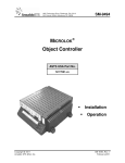
SS-9 General
Service Manual
Stereo Music System
SoundSpace 9
AMFM
Disc
Preset
Random
Track
ST
Memory
Remaining Time
Vol.
i
Repeat
Memory No.
Loud.
SS-9 General
GENERAL
● Floor Stands (Option)
• Floor stand for Main Unit
• Floor stand for Satellite Speakers L/R
1.1. Product Code
D210
Abbreviations for Destinations:
CAN — Canada
CH — China
DA — South America
EP
— Europe
HK
— Hong Kong
JPN — Japan
KR
— Korea
OTR — Other
TW — Taiwan
UK — United Kingdom
USA — U.S.A.
AUS — Australia
1.3. Cautions/Warnings
(1) Product Safety Notice
! in the schematic
Parts marked with the symbol
diagram have critical characteristics.
Use ONLY replacement parts recommended by the manufacturer. It is recommended that the unit be operated from a
suitable DC supply or batteries during initial check-out procedures.
1.2. System Configuration
The SoundSpace consists of the following units.
(2) Leakage Current Check/Resistance Check
Before returning the unit to the customer, make sure you
make either (1) a leakage current check or (2) a line to
chassis resistance check. If the leakage current exceeds
0.5 milliamp, or if the resistance from chassis to either side
of the power cord is less than 240 k ohms, the unit is defective.
WARNING — DO NOT return the unit to the customer
until the problem is located and corrected.
● Main Unit (See pages 1-1, 1-2, ... in this manual)
Controls entire of the System. Mainly consists of the
following sections:
• Control section (including the system control microprocessor)
• Tuner section
• Operation panel control section
• CD player section (including the mechanism control microprocessor)-- 3 identical CD player sections (Interchangeable with each other except for
the Door Cap Ass'y on which the disc number is
written.)
(3) Protection of Eyes from Laser Beam
To protect eyes from invisible laser beam during servicing,
DO NOT LOOK AT THE LASER BEAM on the Changer.
(4) Laser Caution
CAUTION
Adjusting the knobs, switches, and controls, etc. or taking
actions not specified herein may result in a harmful emission of laser beams. This CD Player must be adjusted and
repaired only by qualified service personnel.
● Subwoofer
(See pages 2-1, 2-2, ... in this manual)
• Subwoofer
• Power amp. section
• Power supply section
● Satellite Speakers L/R
(See pages 3-1, 3-2, ... in this manual)
OBSERVERA!
Sådana inställningar av rattarna, omkopplarna eller övriga
kontrollknappar som inte är beskriva i bruksanvisningen
kan resultera i farlig laserutstrålning. Justering eller reparation av denna kompaktskivspelare skall endast utföras av
kvalificerad servicepersonal.
● Main Remote Control/Sub Remote Control
Subwoofer
Speaker L
Remote Control
(Main)
(Sub)
• Power Amp.
• Power Supply
OBS!
Indstilling af knapper, cmskiftere og øvrige kontrolknapper,
som ikke følger den i brugsanvisningen beskrevne måde,
kan resultere i farlig laserudstråling. Justering eller reparation af denno CD-afspiller må kun udføres af kvalificeret
servicepersonale.
Speaker R
OBS!
Justering av ratt, brytere og kontroller andre enn de som er
beskrevet her, kan resultere i farlig laserbestråling. Justering eller reparasjon av denne kompaktdiskspilleren ma
bare utføres av kvalifiserte fagfolk.
Main Unit
• Tuner
• CD Player x 3
HUOMAUTUS
Jos nuppeja, kytkimiä ja säätimiä ym, säädetään tai laitetta
käytetään toisella tavalla kuin on selostettu, tuloksena saattaa olla vaarallista lasersäteiden vuotoa. CD-soittimen
säätö ja korjaus on jätettävä aina asiantuntevan
huoltoteknikon tehtäväksi.
: Floor Stand (Option)
Fig. 1.1 SS-9 System Configuration
ii
SS-9 General
ADVERSEL: USYNLIG LASERSTRÅLING VED ÅBNING.
UNDGÅ UDSAETTELSE FOR STRÅLING.
VARO!:
AVATTAESSA OLET ALTTIINA
NÄKYMÄTTÖMÄLLE
CLASS 1
LASER PRODUCT
LAS-
THIS COMPACT DISC PLAYER IS CLASSIFIED
AS A CLASS 1 LASER PRODUCT.
THE CLASS 1 LASER PRODUCT LABEL IS
LOCATED ON THE REAR EXTERIOR.
ERSÄTEILYLLE.
ÄLÄ KATSO SÄTEESEEN.
VARNING — OSYNLIG LASERSTRÅLNING NAR
DENNA DEL ÄR ÖPPNAD. BETRAKTA
EJ STRÅLEN.
1.4. Handling the Laser Pickup
In case of repair or replacement of the Laser Pickup, pay
attention to the following handling instructions since the laser diode in the Laser Pickup is not resistant to static electricity.
(1)
(2) Discharge of Electricity
Be sure to discharge electricity from objects brought into
contact with the Laser Pickup (i.e., soldering iron, tweezers,
probes, volt-ohm-meter probes, etc.) before starting work
by contacting them with the body chassis. Besides, never
touch the Laser Pickup while power is applied.
Grounding
When you repair a Laser Pickup, first ground the human body, as well as the measuring instruments and
other tools (with particular caution to soldering iron).
What's more, your workbench and floor should desirably be grounded using conductive sheet or copper
plate. See Fig. 1.2.
NOTE: Be careful so as not to let your clothes touch
the Laser Pickup, as static electricity on the
clothes will not be released even if your body
is grounded.
(3) Soldering Iron to be Used
The soldering iron for use in repair work should be: (1) a
ceramic soldering iron, (2) a soldering iron with its metal
part grounded, or (3) a soldering iron whose insulation resistance after five minutes of power application is 10 M-ohm
or more at 500 VDC. Soldering should be completed
promptly, at a soldering iron temperature of 320° max (39
W). A soldering iron heated above this temperature can
break down the laser diode.
Wrist-strap
for Grounding
(NO GOOD)
(GOOD)
1MΩ
Laser Pickup
1MΩ
Conductive Sheet or
Copper Plate
Fig. 1.2 Handling the Laser Pickup
iii
SS-9 General
1.5. Package Ass’y and Accessory Ass’y
(1) Main Unit
Schematic
Ref. No.
Part No.
—
03
02
01
02
03
—
—
—
—
—
—
—
—
—
—
0F05628A
0F05630A
0F05629A
0F05631A
0F05689A
0F05690A
0F05692A
0F05693A
0B85619A
0B85620A
0B90462A
0B90819A
0B90820A
—
0B91071A
—
—
—
—
—
—
—
—
—
—
—
—
—
—
—
—
—
—
—
—
—
—
—
—
—
—
—
—
—
—
—
0D03092B
0D07105A
0D07238A
0D07239A
0D07240A
0D07241A
0D07242A
0D07243A
0D07244A
0D07245A
0D07371B
0D07372B
0D07375A
0D07376A
0D07450A
0D07451A
0D07452B
0D07453A
0D07454A
0D07477A
0F05693A
0H08216A
0H08749A
0H09008E
0H09012A
0H09013A
0H09031A
0J08862A
DA05574A
DG05310A
HA08444A
—
HA08447A
01
Fig. 1.3 Main Unit
iv
Description
Q'ty
Package & Accessory Ass'y
(Main Unit)
Carton Box
Packing Bottom Center
Packing Top Center
Accessory Box
Soft Sheet D Top A
Soft Sheet D Top B
Soft Bag Center
Soft Bag Stand Top
13P DIN Cable 5m
3P RCA Cable 5m
Battery UM4x1
FM Indoor Antenna
Antenna Adaptor
(JPN, OTR, USA, CAN, DA, TW)
Antenna Adapter EP
(UK, AUS, EP, CH, HK, KR)
Poly Bag
Speaker Cable
AC Cord UL (USA, CAN)
AC Cord EP (EP)
AC Cord DA/DU (OTR, DA, TW)
AC Cord DM (JPN)
AC Cord BS/HK (UK, HK)
AC Cord CH (CH)
AC Cord KR (KR)
AC Cord SA (AUS)
Owner’s Manual Japanese
Owner’s Manual English
Template
Owner’s Manual Korean
Owner’s Manual French
Owner’s Manual German
Owner’s Manual Spanish
Owner’s Manual Italian
Template Speaker
AM Loop Antenna
Soft Bag Stand Top
CD Single Adaptor (JPN)
Cable Holder
Stand Holder Cover Center
Stand Pole Cover L67
Stand Pole Cover L82
Base Cover Center DT
Pole Cover Cushion
Screw Ass’y D210
Remote Control Sub Ass’y SS—5
Main Remote Ass’y SS9
(Except UK, EP)
Main Remote Ass’y RDS SS9 (UK, EP)
1
1
1
1
1
2
1
3
1
1
4
1
1
1
1
2
1
1
1
1
1
1
1
1
1
1
1
1
1
1
1
1
1
1
1
1
1
1
1
2
1
1
1
1
1
1
SS-9 General
(2) Subwoofer and Satellite Speakers
Schematic
Ref. No.
01
02
03
04
05
—
—
04
Part No.
—
03
05
02
01
Fig. 1.4 Subwoofer and Satellite Speakers
v
0F05694A
0F05703A
0F05702A
0F05691A
0F05541A
DA05647A
DA05648A
Description
Q'ty
Package and Accessory Ass’y
(Subwoofer and Satellite Speakers)
Carton Box S369
Packing Bottom Subwoofer
Packing Top Subwoofer
Soft Sheet Subwoofer
Soft Bag Satellite
Screw Ass’y S369
Spacer Ass’y S369
1
1
1
1
2
1
1
SS-9 Main Unit Section
Main Unit
Main Unit Section
AMFM
Disc
Preset
Random
Track
ST
Memory
Remaining Time
Vol.
1-1
Repeat
Memory No.
Loud.
SS-9 Main Unit Section
CONTENTS
1.
REMOVAL PROCEDURES ................................................................................................................................1-3
1.1. Rear Cover ............................................................................................................................................. 1-3
1.2. Main P.C.B. Ass'y ..................................................................................................................................1-3
1.3. Mechanism CD Ass'y .............................................................................................................................1-3
1.4. Front P.C.B. Ass'y ..................................................................................................................................1-4
1.5. Mechanism Chassis Block/Door Block of the Mechanism CD Ass'y .................................................... 1-4
1.6. Disc Loading Ass'y .................................................................................................................................1-4
1.7. CD P.C.B. Ass'y and Traverse Mecha Ass'y .........................................................................................1-5
1.8. Laser Pickup .......................................................................................................................................... 1-6
1.9. Sled Motor .............................................................................................................................................. 1-6
2. ELECTRICAL CHECKS ..................................................................................................................................... 1-8
2.1. Measurement Instruments and Jigs ......................................................................................................1-8
2.2. Parts Location for Electrical Check ........................................................................................................1-8
2.3. Electrical checks for CD Player .............................................................................................................1-9
3. MECHANISM ASS'Y AND PARTS LIST ...........................................................................................................1-11
3.1. Main Stand Ass'y ................................................................................................................................... 1-11
3.2. Synthesis (Main Unit) .............................................................................................................................1-12
3.3. Mechanism CD Ass'y 1/Mechanism CD Ass'y 2 (A01) .........................................................................1-14
3.4. Mechanism Chassis Ass'y (B01) ...........................................................................................................1-16
3.5. Traverse Mecha Ass'y (B02) ..................................................................................................................1-17
3.6. Disc Loading Ass'y (B03) .......................................................................................................................1-18
4. ELECTRICAL PARTS LIST ...............................................................................................................................1-20
4.1. Main P.C.B. Ass'y ...................................................................................................................................... 1-20
4.2. Front P.C.B. Ass'y ..................................................................................................................................... 1-20
4.3. CD P.C.B. Ass'y ........................................................................................................................................ 1-21
4.4. LED P.C.B. Ass'y ...................................................................................................................................... 1-21
4.5. SEN LD1 P.C.B. Ass'y ..............................................................................................................................1-21
4.6. SEN LD2 P.C.B. Ass'y ..............................................................................................................................1-21
4.7. SEN UD P.C.B. Ass'y ................................................................................................................................1-21
5. IC BLOCK DIAGRAMS ..................................................................................................................................... 1-22
6. BLOCK DIAGRAM ............................................................................................................................................ 1-33
SPECIFICATIONS (See the end of this manual.)
SCHEMATIC DIAGRAMS AND MOUNTING DIAGRAMS (See the separate volume.)
1-2
SS-9 Main Unit Section
1.
REMOVAL PROCEDURES
NOTE: When parts required lubrication are replaced or reassembled, apply specified lubricant to the parts.
For the parts which require lubrication, refer to 3. "MECHANISM ASS'Y AND PARTS LIST."
1.1. Rear Cover
Refer to Fig. 1.1.
(1) Remove F01 (Main Jack Cover) by pulling it out.
(2) Remove screws F02 (ST3x8 + Binding (Black), 5 pcs.)
and F03 (PT3x10 + Trass, 4 pcs.), and detach F04
(Rear Cover) from the main body.
Main P.C.B. Ass'y
Rear Cover
Fig. 1.1
1.2. Main P.C.B. Ass'y
Refer to Fig. 1.2.
(1) Remove the Rear Cover. Refer to item 1.1.
(2) Remove screws F01 (ST3x4 + Binding, 15 pcs.) and
F02 (M2.6x4 + Binding, 2 pcs.), and detach F03.
(3) Remove screws F04 (ST3x5 + Binding, 10 pcs.) and
F05 (ST2.6x4 + Binding, 2 pcs.), and detach F06
(Main P.C.B. Ass'y).
Notes on reassembling:
• Connect the cables #1, #2 and #3 to the connectors #1,
#2 and #3 on the Main P.C.B. Ass'y, respectively.
Fig. 1.2
1.3. Mechanism CD Ass'y
Refer to Fig. 1.3.
(1) Remove the Main P.C.B. Ass'y. Refer to item 1.2.
(2) Remove screws F01 (M3x8 + Binding (2A), 8 pcs.),
F02 (Damper Collar, 8 pcs.) and F03 (Mecha Damper,
8 pcs.).
(3) Lift the Escutcheon and remove F04 (2 pcs.) from F05
(Mechanism CD Ass'y 1-No. 2) and F06 (Mechanism
CD Ass'y 1-No. 3).
Note: The Mechanism CD Ass'y 2-No. 1 can be removed
in the same way.
Notes on reassembling:
• When assembling the Mechanism CD Ass'y 1-No. 3, with
the Mechanism CD Ass'y 1-No. 2 not assembled yet,
pass the cable of the Mechanism CD Ass'y 1-No. 3 over
the frame "A". Otherwise, you cannot assemble the
Mechanism CD Ass'y 1-No. 3.
• Pass the cables of each Mechanism CD Ass'y through
the holes "B" and "C" as shown in Fig. 1.3. For Mechanism CD Ass'y 1-No. 2/No.3, extend their cables approx.
10 cm.
A
B
Escutcheon
C
Mechanism
CD Ass'y 2
-No. 1
Mechanism
CD Ass'y 1
-No. 3
Mechanism
CD Ass'y 1
-No.2
Fig. 1.3
1-3
SS-9 Main Unit Section
1.4. Front P.C.B. Ass'y
Refer to Fig. 1.4.
(1) Remove the Mechanism CD Ass'y. Refer to item 1.3.
(2) Remove screws F01 (BT2.6x6 + Flat Head, 2 pcs.)
and F02 (PT2.6x8 + Flat Head, 2 pcs.), and detach
F03 (Dress Plate Side C/D).
(3) Remove screws F04 (2 pcs.) and F05 (PT3x8 + Binding, 5 pcs.), and detach F06 (GND Wire Ass'y).
(4) Remove F07 in the direction shown by the arrow while
passing the power switch cable through the hole "A"
and 3 connectors through the hole "B".
(5) Remove F08 (Power Switch) outward while pinching
its claws inward.
(6) Remove screws F09 (PT3x5 + Binding, 4 pcs.) and
F10 (PT3x8 + Binding, 3 pcs.), and detach F11 (Front
P.C.B. Ass’y).
1.5. Mechanism Chassis Block/Door Block of the
Mechanism CD Ass'y
Refer to Fig. 1.5.
(1) Remove the Mechanism CD Ass'y. Refer to item 1.3.
(2) Remove screws F01 (M2.6x5 + Binding, 4 pcs.), unhook the spring F02, and detach F03 (Mechanism
Chassis Block) from the Door Block.
Mechanism Chassis
Block
Notes on reassembling:
• When assembling F08 (Power Switch), be careful so as
not to assemble it upside down.
• When assembling F07, pass the power switch cable
through the hole "A" and 3 cables through the hole "B".
Door Block
Fig. 1.5
A
1.6. Disc Loading Ass'y
Refer to Fig. 1.6.
(1) Remove the Door Block of the Mechanism CD Ass'y.
Refer to item 1.5.
(2) Remove screws F01 (PT2.6x6 + Binding (Black), 4
pcs.), and detach F02 (Disc Loading Ass'y).
B
Front
P.C.B.
Ass’y
Disc Loading Ass'y
Fig. 1.4
Fig. 1.6
1-4
SS-9 Main Unit Section
1.7. CD P.C.B. Ass'y and Traverse Mecha Ass'y
Refer to Figs. 1.7.1 and 1.7.2.
(1) Remove the Mechanism Chassis Block. Refer to item
1.5.
(2) Remove screws F01 (M3x5 + Binding (Black), 4 pcs.),
F02 (Stabi SP) and F03, and detach F04 (Traverse
Mechanism Block). Refer to Fig. 1.7.1.
Laser diode shorting lands
Traverse Mechanism Block
CD P.C.B. Ass’y
Traverse Mecha
Ass’y
Fig. 1.7.2
Fig. 1.7.1
(3)
Remove screws F01 (M2.6x4 + Binding (Black), 3
pcs.), collars F02 (3 pcs.) and one screw F03 (M2.6x4
+ Pan (Black)), and detach F04 (Traverse Cover CD).
Refer to Fig. 1.7.2.
(4) Short the laser diode shorting lands with a soldering
iron.
Note: Use the soldering iron whose metal part is
grounded or a ceramic soldering iron.
CAUTION: Do not disconnect the Flexible Cable from
the CD P.C.B. Ass'y unless the laser shorting lands are shorted.
(5) Remove screws F05 (M3x5 + Binding), 4 pcs.) and detach F06 (CD P.C.B. Ass’y).
(6) Remove three Damper Screw SL and one Damper
Screw SD, and detach F07 (Traverse Mecha Ass'y).
Notes on reassembling:
• Unsolder the laser diode shorting lands after reassembling the CD P.C.B. Ass'y.
1-5
SS-9 Main Unit Section
1.8. Laser Pickup
1.8.1.
Removing the Laser Pickup
Refer to Fig. 1.8.1.
(1) Remove the Traverse Mecha Ass'y. Refer to item 1.7.
(2) Remove screws F01 (M1.7x4 + Pan, 2 pcs.) and F02
(M2.6x3.5 + Pan, 2 pcs.), and F03 (4 pcs.), and disassemble F04 (Laser Pickup Block).
(3) Pull out the PU Guide Shaft SL from the Laser Pickup
Block.
(4) Before disconnecting the Pickup Flexible P.C.B. from
the Laser Pickup, short the laser diode shorting lands
on the bottom of the Laser Pickup. Refer to Fig. 1.8.2.
NOTE: Use the soldering iron whose metal part is
grounded or a ceramic soldering iron.
(5) Disconnect the Pickup Flexible P.C.B. from the Laser
Pickup.
Short
Already shorted.
(See Fig. 1.7.2)
Fig. 1.8.2
1.9. Sled Motor
1.9.1.
Removing the Sled Motor
Refer to Fig. 1.9.1.
(1) Remove the Traverse Mecha Ass'y. Refer to item 1.7.
(2) Remove a cut washer F01 and pull out F02 (Second
Gear).
(3) Remove screws F03 (M1.7x2.5 + Pan #0 Type 3
(Black), 2 pcs.) and detach the Sled Motor Block.
(4) Remove F05 (First Gear) from F04 (Sled Motor).
(5) Unsolder the wires of F04 (Sled Motor) from the Traverse P.C.B. Ass'y.
PU Guide Shaft SL
✪
✪: Apply lubricant
G-4270.
✪: Apply lubricant
G-4270.
✪
Fig. 1.9.1
1.9.2.
Installing a New Sled Motor
(1) Reassemble F04 (Sled Motor) with screws F03 (2
pcs.) with a torque of 2.0 kg-cm.
NOTE: Pay attention to the sled motor installing direction. Install it as shown in Fig. 1.9.1.
(2) Press fit a new F05 (First Gear) so that the gap between the chassis surface and the bottom of F05 (First
Gear) is 0.1 mm as shown in Fig. 1.9.2.
(3) Solder the wires of F04 (Sled Motor) to the Traverse
P.C.B. Ass'y.
(4) Reassemble other removed parts by reversing the removal procedure.
Fig. 1.8.1
1.8.2.
Installing a New Laser Pickup
(1) Connect the Pickup Flexible P.C.B. to the new Laser
Pickup. Refer to Fig. 1.8.2.
(2) Open the laser diode shorting lands on the bottom of
the Laser Pickup.
NOTE: Use the soldering iron whose metal part is
grounded or a ceramic soldering iron.
(3) Insert the PU Guide Shaft SL into the Laser Pickup.
(4) Assemble F04 (Laser Pickup Block) with F03 ( 4 pcs.)
by tightening screws F02 (2 pcs.) with a torque of 3.0
kg-cm.
(5) Assemble F04 (Laser Pickup Block) with screws F01
(2 pcs.) with a torque of 1.2 kg-cm. Refer to Fig. 1.8.1.
Fig. 1.9.2
1-6
SS-9 Main Unit Section
How to reassemble the UD Cam S and UD Cam
How to identify the UD Cam S and UD Cam:
The UD Cam S is used on the left side of the CD Mechanism Ass'y in Fig. A. It has the projections as shown below:
While, the UD Cam is used on the right side of the CD
Mechanism Ass'y in Fig. A, and has not projections.
• Note that they move in the opposite direction each
other. For example, in Fig. A, when the UD Cam S
moves backwards, the UD Cam moves forward.
UD Cam S
Cam D WW Guide
Cam D L Gear
UD Cam S
Projection
Cam D L Gear
Rack
Cam Drive Gear
(1)
Remove the cut washer and pull out the Cam D WW
Gear. Refer to Fig. A.
(2) Remove the cut washer and pull out the Cam D L
Gear. (Thus, the link between the UD Cam S and UD
Cam is lost.)
(3) Assemble the UD Cam S on the chassis so that its
rack engages with the gear on the chassis. Then, by
turning the Cam D L Gear on the chassis, align the
edge of the UD Cam S with the edge of the chassis
as shown in Fig. A. (①)
(4) Assemble the UD Cam on the chassis so that its rack
engages with the gear on the chassis. Then, by turning the Cam Drive Gear on the chassis, align the
edge of the UD Cam with the edge of the chassis as
shown in Fig. A. (➁)
(5) Assemble the Cam D L Gear which was removed in
(2) and engage the cut washer. (Then, the UD Cam
S and UD Cam are linked.) (➂) Refer to Fig. B.
(6) By turning the Cam D L Gear, align the grooves on
the UD Cam S and UD Cam with the center slit of the
chassis as shown in Fig. B. (④)
• Fig. B shows the grooves on the UD Cam. Note
that the shape of the UD Cam S's grooves are reversed.
(7) Assemble the Cam D WW Gear which was removed
in (1) and engage the cut washer. (➄)
Note: If the assembled UD Cam S or UD cam is mis-positioned, the UD Plate S Ass'y (L or R) that engages with its grooves cannot be correctly assembled. In this case, you need to repeat above
steps.
UD Cam
Fig. A
Cam D WW Guide
Cam D L Gear
Grooves on
the UD Cam
Center Slit of the Chassis
Fig. B
1-7
SS-9 Main Unit Section
2.
ELECTRICAL CHECKS
Perform the following electrical checks for CD Players.
2.1. Measurement Instruments and Jigs
(1)
(2)
(3)
(4)
Oscilloscope (40 MHz or more)
DC Voltmeter (Digital Voltmeter)
ABEX Test Disc TCD-784 (DA09195A)
ABEX Test Disc TCD-726A (DA09204A) or TCD-725A
2.2. Parts Location for Electrical Check
● CD P.C.B. Ass'y of the CD Player
(Dip Side View)
R101
Laser Current Check
Pin 1 of TP101
EFM Signal
Fig. 1.1 Parts Location for Electrical Check -- CD Player
1-8
SS-9 Main Unit Section
2.3. Electrical checks for CD Player
Note: Do the same check for CD Player Nos. 1 to 3.
STEP
1
ITEM
SIGNAL
SOURCE
OUTPUT
CONNECTION
Laser Current ABEX Test Disc DC Voltmeter
Check
TCD-784
across R101
ADJUSTMENT
—
REMARKS
1. Turn ON the power and load a test disc.
(To load the test disc, press the Open/Close button
on CD P.C.B.
of the CD Player.)
2. Play back the test disc and calculate the current
flowing into R101 on the CD P.C.B. Ass'y from the
following formula.
Voltmeter Value
I(Measured) =
= oo.o mA
R101 (10 Ohms)
Example:
KSS-540A
510.3 (mV)
I(Measured) =
= 51.03 mA
10 (ohms)
3. Check that the I(Measured) obtained in 2 and the
IOP(oo.omA)
Laser Pickup
rated current value (IOP) shown on the label are
almost the same.
[How to read IOP on the label]
KSS-540A
The shaded "OOO" on the label shows the IOP.
If "OOO" is 475, the IOP is 47.5mA.
NOTE: The calculated current (I(Measured))
should be in a range of 30 to 60 mA. If the
value is large, the pickup will be defective.
4. Stop the test disc.
2
EFM Signal
ABEX Test Disc Oscilloscope
Adjustment
TCD-784
—
between
pin 1 of TP101
1. Play back the first track of the test disc.
2. Be sure that the peak-to-peak value of the EFM
waveform is approx. 1V.
and GND
on CD P.C.B.
Approx. 1Vp-p
Oscilloscope Setting:
AC Mode, 0.2 V/div, 0.5 µs/div
3. Stop the test disc and eject it.
1-9
SS-9 Main Unit Section
STEP
ITEM
SIGNAL
SOURCE
3
Operation
ABEX Test Disc
Check
TCD-726
or TCD-725A
OUTPUT
CONNECTION
ADJUSTMENT
—
REMARKS
Make sure that no noise nor track-jumping is found in
the following programs on the test disc.
To select the desired program, press Track Search
button on the Main Unit or Remote Control
• Interruption 0.8mm:
4th program
• Black dot Ø0.6mm:
8th program
• Simulated fingerprint Ø65µm: 13th program
1-10
SS-9 Main Unit Section
3.
MECHANISM ASS'Y AND PARTS LIST
3.1. Main Stand Ass'y
06
L01
L01
05
04
03
01
L02
02
Fig. 3.1
L02
01
3.1. Main Stand Ass'y
Schematic
Ref. No.
01
02
03
04
05
06
L01
L02
Part No.
—
0J08792A
0H08793B
0H08792B
0H08791D
0H08796B
0H08790C
0E04323A
0E03972A
Description
Main Stand Ass’y (Main Unit)
Base Cushion Center S
Stand Base Center R
Stand Base Center L
Base Joint
Stand Pole
Stand Holder Center
BT4x10 + Oval Countersunk
BT4x12 + Binding
1-11
Q'ty
1
2
1
1
1
1
1
SS-9 Main Unit Section
3.2. Synthesis (Main Unit)
L01
Mechanism CD
Ass'y 2 (A01)
02
Mechanism CD
Ass'y 1 (A01) 01
L01
04
05
06
07
L02
L03
06
L02
L03
08
09
12
13
L04
L03
12
13
L04
06
L15
14
L05
11
03 L02
L03
L02
21
L05
L05
L06
L06
L06
L07
L06
L14
L06
L07
20
L16
15
L07
L07
L12
L07
10
L12
L17
L08
L08
17
16
L09
L13
L09
L08
18
L10
L08
L09
L11
19
Fig. 3.2
1-12
L18
SS-9 Main Unit Section
3.2. Synthesis
Schematic
Ref. No.
01
02
03
04
05
06
07
08
09
10
11
12
13
14
15
16
17
18
19
20
21
—
—
—
L01
L02
L03
L04
L05
L06
L07
L08
L09
L10
L11
L12
L13
L14
L15
L16
L17
L18
Part No.
—
Description
Synthesis (Main Unit)
—
Mechanism CD Ass’y 1
—
Mechanism CD Ass’y 2
0B85919A 2P Connector Ass’y
(Except USA, CAN, TW)
0H08732A Dress panel
0H08733C Dress Plate (Except UK, EP)
0H09023A Dress plate RDS (UK, EP)
0H08739B Dress Plate Side A
0H08730A P Cap Button
HA08578A Escutcheon Ass'y (Except UK, EP)
HA08669A Escutcheon Ass'y (UK, EP)
0H08740B Dress Plate Side C
(Except OTR, USA, CAN, TW)
0H09018A Dress Plate Side D
(OTR, USA, CAN, TW)
0J08600B Mini Jack Plate B
0B70281A Power Switch A8CB
(UK, JPN, AUS, EP, CH, DA, HK, KR)
0J08836A Mecha Damper
0J08837A Damper Collar
BK10352A Front P.C.B. Ass’y
0H08725B Main Jack Cover
0H08724B Rear Cover
0J08599A Mini Jack Plate A
0H07947D Mini Jack Cover
0J08279A Mini Jack Cover SP
BK10318A Main P.C.B. Ass’y DM (JPN)
BK10319A Main P.C.B. Ass’y UL
(USA, CAN, DA, TW)
BK10320A Main P.C.B. Ass’y EP
(UK, AUS, EP, CH, HK, KR)
BK10321A Main P.C.B. Ass’y OTR (OTR)
0B85522A GND Wire Ass’y
0J08799A Shield Sheet Center A
0J08800A Shield Sheet Center B
0B85934A 12P Connector Ass’y
0E04237A PT3x12 Dress Screw
0E04346A BT2.6x6 + Flat Head
0E04326A PT2.6x8 + Flat Head
0E04176A M3x8 + Binding (2A)
0E04362A PT3x5 + Binding
0E03731A PT3x8 + Binding
0E04324A ST3x4 + Binding
0E04133A PT3x10 + Trass
0E03281A ST3x8 + Binding (Black)
0E04320A PT2x8 + Binding
0E00029A Washer 2x6x0.4
0E00877A ST3x5 + Binding
0E03283A ST3 x 6 + Binding (Black)
0E04325A ST3x4 + Binding (Black)
0E04174A PT2X5 + Binding
0E00866A M2.6x4 + Binding
0E03749A PT3x8 + Binding (Black)
0E03573A ST2.6x4 + Binding
Q'ty
1
2
1
1
1
1
1
3
1
1
1
1
1
1
12
12
1
1
1
1
1
1
1
1
1
1
1
1
1
3
1-13
SS-9 Main Unit Section
3.3. Mechanism CD Ass'y 1/Mechanism CD Ass'y 2 (A01)
01
L04
02
L03
09
08
11
10
03
04
Traverse Mecha Ass'y
(B02) 12
05
L05
L05
13
16
06
L08
L01
Disc Loading Ass'y
(B03) 07
14
L06
L06
Mechanism Chassis
Ass'y (B01) 15
L02
L02
17
L07
L09
Fig. 3.3
1-14
L07
SS-9 Main Unit Section
3.3. Mechanism CD Ass'y 1 (A01)
Schematic
Ref. No.
A01
01
02
03
04
05
06
07
08
09
10
11
12
13
14
15
16
17
L01
L02
L03
L04
L05
L06
L07
L08
L09
Part No.
—
HG08576A
HG08577A
0H08735C
0H08736C
0J08729B
0H08734B
0H08812A
CA09459A
0C10450B
0C10575A
0C10449A
0C10287A
CA09504A
0C10448A
BK10349A
—
0C10578A
HA08656B
0E04174A
0E04035A
0E03197A
0E00945A
0E03270A
0E00964A
0E03950A
0E00174A
0E04308A
Description
3.3. Mechanism CD Ass'y 2 (A01)
Schematic
Ref. No.
Q'ty
Mechanism CD Ass’y 1
2
A01
Door Cap Ass’y 2 (for Unit No. 2)
Door Cap Ass’y 3 (for Unit No. 3)
Dress Plate Door A
Window Door
D. Cap Spring
Escutcheon Door
Illumination Lens
Disc Loading Ass’y
Traverse Cover CD
Sleeve 4x2.7x2.1
Damper Screw SD
Damper Screw SL
Traverse Mecha Ass’y
D Unit Base
CD P.C.B. Ass’y
Mechanism Chassis Ass’y
Stabi SP
F Panel ME CD S Ass’y
PT2x5 + Binding
PT2.6x6 + Binding (Black)
M2.6x4 + Pan (Black)
M2.6x4 + Binding (Black)
M3x5 + Binding (Black)
M3x5 + Binding
M2.6x5 + Binding
Earth Lug B-4
M2x3.5 + Pan #0 Type 3
1
1
1
1
9
1
1
1
1
3
1
3
1
1
1
1
1
1
01
02
03
04
05
06
07
08
09
10
11
12
13
14
15
16
17
L01
L02
L03
L04
L05
L06
L07
L08
L09
1-15
Part No.
—
HG08549A
0H08824C
0H08736C
0J08729B
0H08734B
0H08812A
CA09459A
0C10450B
0C10575A
0C10449A
0C10287A
CA09504A
0C10448A
BK10349A
—
0C10578A
HA08656B
0E04174A
0E04035A
0E03197A
0E00945A
0E03270A
0E00964A
0E03950A
0E00174A
0E04308A
Description
Q'ty
Mechanism CD Ass’y 2
1
Door Cap Ass’y 1 (for Unit No. 1)
Dress Plate Door B
Window Door
D. Cap Spring
Escutcheon Door
Illumination Lens
Disc Loading Ass’y
Traverse Cover CD
Sleeve 4x2.7x2.1
Damper Screw SD
Damper Screw SL
Traverse Mecha Ass’y
D Unit Base
CD P.C.B. Ass’y
Mechanism Chassis Ass’y
Stabi SP
F Panel ME CD S Ass’y
PT2x5 + Binding
PT2.6x6 + Binding (Black)
M2.6x4 + Pan (Black)
M2.6x4 + Binding (Black)
M3x5 + Binding (Black)
M3x5 + Binding
M2.6x5 + Binding
Earth Lug B-4
M2x3.5 + Pan #0 Type 3
1
1
1
9
1
1
1
1
3
1
3
1
1
1
1
1
1
SS-9 Main Unit Section
3.4. Mechanism Chassis Ass'y (B01)
L01
01
12
L04
L05
20
13
L02
14
L03
02
L04
L04
04
05 ★
09 ✪
L03
06 ★
★ 03
10
11
L03
★ 07
L06
★
★ 08
L01
★
★
07
17
★
15
★18
★16
★ 19
★: Apply lubricant FL-955
✪: Apply lubricant G-4270
Lubricant:
We suggest that you use FL955/G-4270 or equivalent type.
Please contact:
Kanto Chemicals Co. Ltd., 27 Kanda Sakuma-cho,
Chiyoda-Ku, Tokyo, Japan
★
✪
Approx. 10mm
19 ★
★
18★
★
★
Approx. 10mm
17
Fig. 3.4
3.4. Mechanism Chassis Ass'y (B01)
Schematic
Ref. No.
B01
Part No.
—
01
02
03
04
05
06
07
08
09
10
11
12
13
14
15
16
17
18
0C10437A
0C10435A
0C10439C
BK10424A
0C10441A
0C10443A
0C10440A
0C10442A
CA09458A
0C10444A
0C10446A
0B85683A
CA09511A
0C10447A
0C10436A
0C10438A
CA09472A
0C10496A
Description
Mechanism Chassis Ass’y
UD Cam Guide
Cam Guide Chassis S
UD Cam S
SEN UD P.C.B. Ass’y
Cam D L Gear
Cam D WW Guide
Cam Drive Gear
Cam D S Gear
WP Base S Ass'y
Cam D Worm Pulley
Belt 1.5S D18.5
2P Wire Ass’y UD_MOT
UD Motor SD S Ass'y
Cam Motor Holder
Cam Guide Chassis L
UD Cam
UD Plate S Ass’y
UD Cam Roller
Schematic
Ref. No.
Q'ty
1
19
20
L01
L02
L03
L04
L05
L06
1
1
1
1
2
1
4
1
1
1
1
1
1
1
1
1
2
6
Part No.
0C10514A
0C10265A
0E03270A
0E04085A
0E03955A
0E03964A
0E03700B
0E03953A
Description
Apply FL-955:
03,05-08: Whole surface
10:
Worm gear only
16:
Whole surface
17:
2 places (on the left)
18,19:
Whole surface
—:
Chassis (8 places)
1-16
Q'ty
UD Cam Roller S
Motor Grommet SL
M3x5 + Binding (Black)
M2x3.5 (Black)
Cut Washer 2.2x4.2x0.2
ST2.6x3 + Pan #0 Type 3
Coating Clip
M2x2 + Pan #0 Type 1 (Black)
2
1
Apply G-4270:
09: Shaft
—: Chassis's shafts
(4 pcs.)
SS-9 Main Unit Section
3.5. Traverse Mecha Ass'y (B02)
L01
L01
01
02
L01
03
L02
L03
04
04
07
06
05
✪ G-4270
L02
15
14
08
L04
09
✪: Apply lubricant G-4270.
Apply G-4270:
05: Shafts (3 pcs.)
11: Shaft holes (2 places)
Lubricant:
We suggest that you use G-4270
or equivalent type.
Please contact:
Kanto Chemicals Co. Ltd., 2-7
Kanda Sakuma-cho, ChiyodaKu, Tokyo, Japan
10
✪
13
G-4270
11
L05
13
12
L05
Fig. 3.5
3.5. Traverse Mecha Ass'y (B02)
Schematic
Ref. No.
B02
01
02
03
04
05
06
07
08
09
10
11
12
Part No.
Description
CA09504A Traverse Mecha Ass'y
0C10139B
0C09923C
0C10140B
0C10279A
CA09364A
BA09777A
0B84608A
3B90704A
0C10141C
0C10277A
0B90741A
0B61355A
Second Gear
Power Gear
Third Gear
Damper S SL
Disc Motor Chassis Ass'y
Traverse P.C.B. Ass'y
8P Flexible Wire
Sled Motor
Rack CA
PU Guide Shaft SL
Pickup KSS-540A
Pick up Flexible P.C.B.
Schematic
Ref. No.
13
14
15
L01
L02
L03
L04
L05
Q'ty
1
1
1
1
4
1
1
1
1
1
1
1
1
1-17
Part No.
0C10278A
0C10282A
0C10138B
0E04343B
0E03845A
0E00955A
0E00887A
0E03947A
Description
Shaft Lock Plate SL
PU Guide Plate H SL
First Gear
Cut Washer 1.6x3.2x0.2 (Black)
M1.7x2.5 + Pan #0 Type 3 (Black)
BT2x4 + Binding
M1.7x4 + Pan
M2.6x3.5 + Pan (#0 Type 3)
Q'ty
4
1
1
SS-9 Main Unit Section
L01
3.6. Disc Loading Ass'y (B03)
01
L02
02
L03
L01
03 ★
L01
09
★
L04
04★
03
L05
05 ★
★ 10
L04
★06
11
★12
L01
L04
★
06★
L01
15
07
L02
08
L06
★
13
17
16
18
L10
L17
L07 L08
L02
14
19
L06
24
20
21
L09
L04
★
26
L04
25
L12
L11
★11
22
29
L13
L01
L13
30
31
23
32
33
54
34
27
★ 35
28
L10
L12
26 ★
L11
11
46
★
37★
47
★
48
L02
38 ★
36
39
★: Apply lubricant FL-955
Lubricant:
We suggest that you use grease
FL-955 or equivalent type.
Please contact:
Kanto Chemicals Co. Ltd., 2-7
Kanda Sakuma-cho, ChiyodaKu, Tokyo, Japan
L15
★49
★ 50
52
40
44
41
51
★ 42
53
45 ★
43
L10
L14
Fig. 3.6
1-18
L02
L16
SS-9 Main Unit Section
3.6. Disc Loading Ass'y (B03)
Schematic
Ref. No.
B03
01
02
03
04
05
06
07
08
09
10
11
12
13
14
15
16
17
18
19
20
21
22
23
24
25
26
27
28
29
30
31
32
33
34
35
Part No.
Description
CA09459A Disc Loading Ass’y
BK10421A
0C10518A
0C10510A
0C09988B
0C10456A
CA09462A
0C10458A
0C10457A
0C10465A
0C10562A
0C10466A
0C10511A
0C10464A
BK10422A
BK10423A
0C10567A
CA09461A
0C10459A
0C10461A
0C10460A
0C10455A
0C09922B
0C09997B
CA09460A
0C10561A
0C10215A
CA09467A
CA09468A
0C10491B
0C10493A
0C10490A
0C10492B
0C10255A
0C10252A
0C10454A
LED P.C.B. Ass’y
Link Cover
Clamp Holder
Clamp Top
Clamp Arm L
Clamp Link S Ass’y
Clamper RE SP SD
Clamp Arm S
LDG D Cam SP
LDG Cam Tip
LDG Guide Roller
D Sens Cam
LDG D Cam Holder
SEN LD1 P.C.B. Ass’y
SEN LD2 P.C.B. Ass’y
Edge Protector
D Sens Link S Ass’y
Dsens Arm Base
Dsens Arm SP
Disc Sens Arm
Disc Guide SD
Disc Cramp Base
Steel Ring
Loading Chassis SD S Ass’y
LDG Cam Roller
LP Slider SL
Loading Plate L SD S Ass’y
Disc G L SD S Ass’y
D Shutter Base
D Shutter Shaft
D Shutter
D Shutter SP
Shutter Arm Cushion SL
Loading Return Spring SL
LDG Center Guide SD
Schematic
Ref. No.
36
37
38
39
40
41
42
43
44
45
46
47
48
49
50
51
52
53
54
L01
L02
L03
L04
L05
L06
L07
L08
L09
L10
L11
L12
L13
L14
L15
L16
L17
Q'ty
1
1
1
2
1
1
2
1
1
1
1
5
1
1
1
1
1
1
1
1
1
1
1
1
1
1
2
1
1
1
1
1
1
1
1
1
Apply FL-955:
03: Whole surface
04: Whole surface
05: Around the hole
06: Whole surface
08: Around the hole
10: Whole surface
11: Whole surface (4 pcs. only)
12: Holes (5 places)
26: Whole surface
35: Whole surface
37: Whole surface
38: Whole surface
42: Whole surface
45: Whole surface
47: Worm gear only
49: Whole surface
50: Whole surface
1-19
Part No.
CA09464A
0C10191A
0C10192A
0C10193A
0C10476B
0C10477A
0C10213A
0C10478A
CA09465A
0C10479A
0C10488A
CA09512A
0C10265A
0C10236A
0C10237A
0C10563A
CA09470A
0C10480A
0B85682A
0E04085A
0E03964A
0E03943A
0E03954A
0E03243A
0E03700B
0E00869A
0E03461A
0E03970A
0E03955A
0E03961A
0E04310A
0E04119A
0E03969A
0E03953A
0E03845A
0E04075A
Description
Loading Plate R SD S Ass’y
Idler Pulley SL
Pulley Fork SL
Pulley Spring SL
LDG Guide R SD
Timing Belt SD
Timing Gear SL
Loading Link B SD
Loading Link A S Ass’y
LDG Idle Gear SD
LDG Motor Holder
Loading Motor SD S Ass'y
Motor Grommet SL
Loading Worm Gear SL
Loading Sensor Ring SL
LDG Motor Cover
Loading Motor Chassis S Ass’y
LDG Gear Collar SD
2P Wire Ass’y LD_MOT
M2x3.5 (Black)
ST2.6x3 + Pan (#0 Type 3)
BT1.7x5 + Pan #0 Type 3 (Black)
Cut Washer 1.6x3.2x0.2
M2x2.5 + Pan
Coating Clip
BT2.6x4 + Binding
BT2x2.5 + Pan (Black)
M2.6x3 + Pan #0 Type 3
Cut Washer 2.2x4.2x0.2
BT2x4 + Pan #0 Type 1 (Black)
E Ring 1.5mm
Washer 1.2x3x0.25
M1.4x3 + Pan #0 Type 3
M2x2 + Pan #0 Type 1
M1.7x2.5 + Pan #0 Type 3 (Black)
M2x3.5 + Pan #0 Type 1 (Black)
Q'ty
1
1
1
1
1
1
1
1
1
1
1
1
1
1
1
1
1
1
1
SS-9 Main Unit Section
4.
ELECTRICAL PARTS LIST
NOTES: 1. Abbreviations
TR – Transistor, SID – Silicon Diode, ZD – Zener Diode, Varicap – Variable Capacitance Diode
RK – Carbon Resistor, RM – Metal Film Resistor, RF – Fail Safe Type Resistor,
RC – Cement Resistor, CE – Electrolytic Capacitor, CML – Mylar Capacitor,
CC – Ceramic Capacitor, CPP – PP Capacitor, CMM – Metalized Mylar Capacitor,
CSP – Polystyrene Capacitor, C – Mica Capacitor, CT – Tantalum Capacitor
2. Description of capacitor: 10 16V = 10µ 16V
3. Parts marked with * show chip parts.
4.1. Main P.C.B. Ass'y
Schematic
Ref. No.
Part No.
Description
BK10318A Main P.C.B. Ass’y DM
(JPN)
BK10319A Main P.C.B. Ass’y UL
(USA, CAN, DA, TW)
BK10320A Main P.C.B. Ass’y EP
(UK, AUS, EP, CH, HK,
KR)
BK10321A Main P.C.B. Ass’y OTR
(OTR)
U102
U103
U151
U152
U153
U201,202
U203
U204
U205,206
U207
U208
U209
U210
U211
U212
U306
U307
U310,311
U312,313
U501
U502
0B10879A
0B11240A
0B11240A
0B17033A
0B06124A
0B10812A
0B06124A
0B10814A
0B06124A
0B12879A
0B12878A
0B11713A
0B17034A
0B17047A
0B06124A
0B06370A
0B12811A
0B06124A
0B06124A
0B11609A
0B12863A
U503
0B12841A
U504,505
U506
U507
U631
U632
U633
0B12864A
0B12864A
0B17026A
0B11602A
0B13319A
0B10824A
U803
U807
ICP501
0B12883A
0B12783A
0B11639A
Q201L,R
Q301L,R
Q302
Q303L,R
Q304L,R
Q305
Q501
Q502
Q503
Q504
Q505
Q506
Q507
Q508
Q509
0B14186A
0B14186A
0B14186A
0B14186A
0B14186A
0B14186A
0B14002A
0B10357A
0B14167A
0B14013A
0B14002A
0B14004A
0B14167A
0B14013A
0B14002A
IC
NJM2114D
IC
NJM78L05A
IC
NJM78L05A
IC
NJM78M12FA
IC
NJM4558D
IC
LC78211
IC
NJM4558D
IC
LC78213
IC
NJM4558D
IC
TC9459N
IC
TC9184AP
IC
UPC4570C
IC
NJM78M15FA
IC
NJM79M15FA
IC
NJM4558D
IC
NJM4556D
Toslink TOTX178A
IC
NJM4558D
IC
NJM4558D
IC
NJM78M05A
IC
UPD78F4225GC-8*
IC
LC72722PM*
(UK, AUS, EP, CH, HK,
KR)
IC
PQ30RV2
IC
PQ30RV2
IC
NJM78L08A
IC
TC74HC02AF
IC
TC74HC4538AF*
IC
Photocoupler
PC918X
IC
LC89055W*
IC
AD1855*
IC Protector
ICP-N25 1.0A
TR 2SC4213 B*
TR 2SC4213 B*
TR 2SC4213 B*
TR 2SC4213 B*
TR 2SC4213 B*
TR 2SC4213 B*
TR DTA114EK*
TR DTB113ES
TR 2SC2412K*
TR DTC144EK*
TR DTA114EK*
TR DTA144EK*
TR 2SC2412K*
TR DTC144EK*
TR DTA114EK*
Schematic
Ref. No.
Q518,519
Q520
Q521
Q522
Q523,524
Q525
Q526
Q601
Q602
Q603
Q604
Q605
Q606
Q607,608
Q609
Q610
Q611,612
Q631
ZD501
D201,202
D203
D501,502
D503
D505,506
D507,508
D509,510
D601,602
D603
D631,632
D633
L151,152
L501
L801,802
L803
L805
L806
X501
X502
X801
R250,251
R501
R511
R513
R514
R552
R559
R573
R576
Part No.
Description
0B10882A TR DTC114TKA*
0B14013A TR DTC144EK*
0B14013A TR DTC144EK*
(UK, AUS, EP, CH,
HK, KR)
0B14013A TR DTC144EK*
0B10882A TR DTC114TKA*
0B14013A TR DTC144EK*
0B14011A TR DTC114EK*
0B14002A TR DTA114EK*
0B14013A TR DTC144EK*
0B14004A TR DTA144EK*
0B14002A TR DTA114EK*
0B14013A TR DTC144EK*
0B14167A TR 2SC2412K*
0B10882A TR DTC114TKA*
0B14002A TR DTA114EK*
0B14011A TR DTC114EK*
0B14013A TR DTC144EK*
0B14167A TR 2SC2412K*
0B12147A ZD RD5.1V JS B2
0B12249A SID 1SS133
0B12249A SID 1SS133
0B12249A SID 1SS133
0B12725A SID 1SR139-100
0B12249A SID 1SS133
0B12249A SID 1SS133
0B12249A SID 1SS133
0B12249A SID 1SS133
0B12249A SID 1SS133
0B12249A SID 1SS133
0B12249A SID 1SS133
0B51183A Inductor 100uH
0B51369A Inductor 10mH
0B51392A Inductor 47uH
0B51392A Inductor 47uH
0B51392A Inductor 47uH
0B51159A Inductor 1uH
0B91047A X’tal 8.38MHz
0B90889A X’tal 4.3320MHz
(UK, AUS, EP, CH,
HK, KR)
0B90902A X’tal 12.288MHZ
0B24365R RF 10
1/4W J
0B24365R RF 10
1/4W J
0B25612A RK 0
1/10W J*
(USA, CAN, DA, TW)
0B25563A RK 10K
1/10W J*
(OTR)
0B25612A RK 0
1/10W J*
(JPN)
0B24498R RF 120
2W
0B25612A RK 0
1/10W J*
(JPN, OTR, USA, CAN,
DA, TW)
0B25539A RK 1K
1/10W J*
(UK, AUS, EP, CH, HK,
KR)
0B25539A RK 1K
1/10W J*
(UK, AUS, EP, CH, HK,
KR)
1-20
Schematic
Ref. No.
R577
R676
C353L
C353R
C506
C519
C520
C521
C522
C523
C524
CP151
CP508
MJ201
MJ301
MJ501
PJ301
PJ302
PJ303
PJ304
Part No.
Description
0B25539A RK 1K
1/10W J*
(UK, AUS, EP, CH, HK,
KR)
0B09995A RF 0.22 2W
0B43387A CPP 120P 100V J
(UK, AUS, EP, CH, HK,
KR)
0B43387A CPP 120P 100V J
(UK, AUS, EP, CH, HK,
KR)
0B42247A CE 0.1 5.5V F
0B40871A CE 10 16V
(UK, AUS, EP, CH, HK,
KR)
0B43092A CC 0.1 25V Z*
(UK, AUS, EP, CH, HK,
KR)
0B43206A CC 560P 50V J*
(UK, AUS, EP, CH, HK,
KR)
0B43061A CC 22P 50V J*
(UK, AUS, EP, CH, HK,
KR)
0B43061A CC 22P 50V J*
(UK, AUS, EP, CH, HK,
KR)
0B43092A CC 0.1 25V Z*
(UK, AUS, EP, CH, HK,
KR)
0B84330A F Connector 15P
5597-15CPB
0B81459A 2P T-Post (UK, AUS, EP,
CH, HK, KR)
0B80774A Mini Jack H
0B80774A Mini Jack H
0B80774A Mini Jack H
0B85629A 2P Pin Jack AU W R
0B85450A 6P Pin Jack AU W R
0B85910A 1P Pin Jack AU BLK
0B85629A 2P Pin Jack AU W R
0B90949A Tuner Pack TFCE1 DM
(JPN) (1)
0B90950A Tuner Pack TFCE1 UL
(USA, CAN, DA, TW) (1)
0B90951A Tuner Pack TFCE1 EP
(UK, OTR, AUS, EP, CH,
HK, KR) (1)
0B80668A DIN 13P Socket (1)
4.2. Front P.C.B. Ass'y
Schematic
Ref. No.
Part No.
Description
BK10352A Front P.C.B. Ass’y
U701
U702
U703
Q701
Q702
D701
0B12803A
0B10961A
0B13257A
0B10068A
0B10015A
0B12745A
IC
LC7584E
IC
NJU3713G*
IR SENSOR 38K
TR DTC114ES
TR 2SA1020 (O,Y)
SID MA719
SS-9 Main Unit Section
Schematic
Ref. No.
LCD701
LED701
LED702
LED703
LED704
LED705
LED706
LED707
LED708
LED709
LED710
LED712
HJ301
SW901,902
SW903,904
SW905
SW908,909
SW910,911
SW912,913
4.4. LED P.C.B. Ass'y
Part No.
0B90913B
0B12806A
0B12806A
0B12806A
0B12806A
0B12806A
0B12806A
0B12806A
0B12865A
0B12865A
0B12865A
0B10825A
0B85811A
0B70295A
0B70295A
0B70282A
0B70295A
0B70295A
0B70295A
Description
LCD DLC-A1622P
LED Green
LED Green
LED Green
LED Green
LED Green
LED Green
LED Green
LED WHITE
LED WHITE
LED WHITE
LED Amber GL3HS43
Mini Jack SW1
Tact Switch SKQBLB
Tact Switch SKQBLB
Tact Switch
Tact Switch SKQBLB
Tact Switch SKQBLB
Tact Switch SKQBLB
U101
U102
U103
U104
U105,106
U180
U501
U502
U601
Q101
Q102
Q103
Q106
Q403
Q404
Q411,412
Q413
Q414
Q501,502
Q503,504
Q505
ZD401
ZD403
ZD404,405
D101,102
D404
D406
L101
L102,103
L104
L105
L503
L601
X101
X501
C411
CP101
CP102
Part No.
Description
BK10349A CD P.C.B. Ass’y
0B10691A
0B10948A
0B10953A
0B12955A
0B10719A
0B10645A
0B12988A
0B11928A
0B10832A
0B10731A
0B14013A
0B10652A
0B12847A
0B10901A
0B10930A
0B14167A
0B14167A
0B10930A
0B14013A
0B12847A
0B12847A
0B12150A
0B12153A
0B12150A
0B10540A
0B10540A
0B10540A
0B51300A
0B50287A
0B51138A
0B51183A
0B50287A
0B50287A
0B90672A
0B91047A
0B42247A
0B80896A
0B85680A
LED1
LED2
LED3
SW1
IC
CXA2521Q*
IC
CXD2587Q*
IC
TC4W53FU*
IC
BA5983FP*
IC
TA8409F*
IC
NJM2100M*
IC
UPD78018FGC*
IC
TC4049BF
IC
TC74HCU04AF*
TR 2SB1132*
TR DTC144EK*
TR DTC144TK*
TR 2SK2158*
TR 2SD2153TL*
TR 2SD1758F*
TR 2SC2412K*
TR 2SC2412K*
TR 2SD1758F*
TR DTC144EK*
TR 2SK2158*
TR 2SK2158*
ZD RD5.6V JS B2
ZD RD6.2V JS B2
ZD RD5.6V JS B2
SID MA152WA*
SID MA152WA*
SID MA152WA*
Inductor 10uH
Coil 120uH*
Inductor 1mH
Inductor 100uH
Coil 120uH*
Coil 120uH*
X’tal 16.9344MHz
X’tal 8.38MHz
CE 0.1 5.5V F
16P F Connector*
8P F Connector*
Part No.
Description
BK10421A LED P.C.B. Ass’y
0B12900A
0B12900A
0B13141A
0B70302A
LED BLUE
LED BLUE
LED GREEN
Tact Switch
4.5. SEN LD1 P.C.B. Ass'y
Schematic
Ref. No.
Part No.
Description
BK10422A SEN LD1 P.C.B. Ass’y
PC1,2
0B10737A IC Photointerrupter
4.6. SEN LD2 P.C.B. Ass'y
Schematic
Ref. No.
4.3. CD P.C.B. Ass'y
Schematic
Ref. No.
Schematic
Ref. No.
PC3
Part No.
Description
BK10423A SEN LD2 P.C.B. Ass’y
0B10737A IC Photointerrupter
4.7. SEN UD P.C.B. Ass'y
Schematic
Ref. No.
PC4,5
Part No.
Description
BK10424A SEN UD P.C.B. Ass’y
0B10737A IC Photointerrupter
1-21
SS-9 Main Unit Section
5.
IC BLOCK DIAGRAMS
• System Controller (U502 µPD78F4225GC-8)
Pin No.
1
2
3
4
5
6
7
8
9
Signal Name
P15
MASTER
H.PIN
AVss
INH1
LCE1
AVref1
RDI
RDO
I/O
—
I
I
—
O
O
—
I
O
10
RCK
O
11
12
13
14
15
16
NC
NC
NC
DIFCE
DIFRES
CD-SI
—
—
—
O
O
I
17
CD-SO
O
18
CD—SCK
I
19
20
21
22
23
24
25
26
27
28
29
30
31
32
33
34
35
36
37
38
CD3RES
CD2RES
CD1RES
CD3CE
CD2CE
CD1CE
CD3EJC
CD2EJC
CD1EJC
NC
NC
LEDSTB
NC
L.STBY
Vss1
NC
NC
ST-VOL
ST-TONE
ST-AN
O
O
O
O
O
O
I
I
I
—
—
O
—
O
—
—
—
O
O
O
39
A-EN
O
Function
Grounded.
Remote controller's Main/Remote detect signal.
Headphone connection detect signal.
GND.
LCD/LED display inhibit signal.
Chip enable signal to the LCD driver.
Reference voltage.
Serial data input from the PLL and RDS ICs.
Serial data output to the PLL, RDS, LCD, VOL, LED
and DIR ICs.
Serial clock output to the PLL, RDS, LCD, VOL, LED
and DIR ICs.
Not used.
Not used.
Not used.
Strobe output to the DIR IC.
Reset output to the DIR IC.
Serial data input from the CD Mechanism.
(Serial data input for flash ROM writing)
Serial data output to the CD Mechanism.
(Serial data output for flash ROM writing)
Serial clock input from the CD Mechanism.
(Serial clock input for flash ROM writing)
Reset signal to the Mechanism CD Ass'y (No. 3).
Reset output to the Mechanism CD Ass'y (No. 2).
Reset output to the Mechanism CD Ass'y (No. 1).
Chip enable output to the Mechanism CD Ass'y (No. 3).
Chip enable output to the Mechanism CD Ass'y (No. 2).
Chip enable output to the Mechanism CD Ass'y (No. 1).
Eject key input from the Mechanism CD Ass'y (No. 3).
Eject key input from the Mechanism CD Ass'y (No. 2).
Eject key input from the Mechanism CD Ass'y (No. 1).
Not used.
Not used.
Strobe signal to the LED IC.
Not used.
Standby LED ON/OFF control signal.
GND.
Not used.
Not used.
Strobe output to the Volume IC.
Strobe output to the Tone IC.
Strobe output to the audio source switching and
Rec-out switching ICs.
Serial signal transmission permit output to the VOL,
TONE, AN ICs.
1-22
Active
Standby
L
H
—
—
L
H
L
L
L/H
L/H
—
L
L/H
L
H
H
L/H
L
L
—
L/H
L
L/H
L
H
H
H
H
H
H
L
L
L
L
L
L
L
L
L
—
—
—
L
L
L
L
H
H
H
L
L
L
H
L
SS-9 Main Unit Section
• System Controller-Continued (U502 µPD78F4225GC-8)
Pin No.
40
41
42
43
44
45
46
47
48
49
50
51
52
53
54
55
56
57
58
59
60
61
62
63
64
65
66
67
68
69
70
71
72
73
74
75
76
77
78
79
80
Signal Name
NC
ENCDMU-M
ENCDMU-R
MUTE-M
MUTE-R
MUTE-PH
NC
NC
P-ON
REM
NC
NC
TCE
RDSCE
T-EN
NC
SD
ST
SYNC
RDSID
RESET
NC
P-OFF
PWR-SW
NC
NC
AD-PWR
Vss0
Vdd1
X2
X1
TEST/Vpp
XT2
XT1
Vdd0
Avdd
AREA
MODEL
KI1
KI0
SMETER
I/O
—
O
O
O
O
O
—
—
O
I
—
—
O
O
O
—
I
I
I
I
I
Function
Not used.
Main room muting permit output signal from the CD.
Remote room muting permit output signal from the CD.
Main room muting output.
Remote room muting output.
Headphone muting output.
Not used.
Not used.
Power ON control output.
Remote sensor input.
Not used.
Not used.
Chip enable signal to the PLL IC.
Chip enable signal to the RDS IC.
Communication permit output between the PLL IC.
Not used.
SD input from the PLL IC.
Stereo input from the PLL IC.
RDS sync input.
RDS ID input.
Reset input.
—
I
I
—
—
O
—
—
—
—
—
—
—
—
—
I
I
I
I
I
Not used.
Power OFF detect signal.
AMP power switching control input.
Not used.
Not used.
AD Power ON output.
GND.
+5V.
8.38MHz X'tal is connected.
8.38MHz X'tal is connected.
(For testing)
Not used.
Grounded.
+5V.
+5V.
Area selection input.
Model selection input.
Key input 1 signal.
Key input 2 signal.
S-meter input signal from the PLL IC.
1-23
Active
Standby
H
H
L
L
L
L
L
L
L
L
H
L/H
L
—
H
H
H
L
L
L
L
L
L
L
L
—
—
—
—
—
L
L
—
—
L
H
—
—
—
—
—
—
—
—
—
—
SS-9 Main Unit Section
• Mechanism Controller (U501 µPD78018FGC)
Pin No.
1
2
3
4
5
6
7
8
9
10
11
12
13
14
15
16
17
18
19
20
21
22
23
24
25
26
27
28
29
30
31
32
33
34
35
36
37
38
39
40
41
42
43
44
45
Signal Name
LSI DATA
LSI CLK
LSI XLT
SCLK
CDRST
EN CLK
IR
LD ON
VSS
P40
P41
ML
MC
MD
DACRST
MVCONT
P47
DISCIN
P51
UD
HOME
LDLOAD
LDEJECT
VSS
UDUP
UDDOWN
P60
P61
P62
P63
L EJ
MUTE
L-BLUE
L-GREEN
RESET
P00
SHUTTER
LOAD
SCOR
VDD
X2
X1
IC
XT2
P04
I/O
O
O
O
O
O
O
O
O
—
—
—
O
O
O
O
O
—
I
—
I
I
O
O
—
O
O
—
—
—
—
O
O
O
O
I
—
I
I
I
—
—
—
—
—
I
Function
DSP command data output.
DSP command clock output.
DSP command latch pulse output.
DSP servo parameter readout clock.
DSP reset output.
DSP clock ON/OFF output.
Interruption countermeasure circuit ON/OFF control
output.
Laser ON/OFF control output.
GND.
(For testing, etc.)
(For testing, etc.)
Latch output to the DAC IC.
Serial clock output the DAC IC.
Serial data output to the DAC IC.
DAC reset output.
Loading speed setting output. ( H=7V, L=5V )
Not used.
Mechanism loading sensor input.
Not used.
Mechanism Up/Down sensor input.
Mechanism Up/Down sensor input.
Mechanism loading motor drive output.
Mechanism loading motor drive output.
GND.
Mechanism Up/Down motor drive output.
Mechanism Up/Down motor drive output.
Not used.
Not used.
Not used.
Not used.
Eject LED ON/OFF control output.
Audio mute output.
Blue illumination ON output.
Green illumination ON output.
Reset input.
Grounded.
Mechanism loading sensor input.
Mechanism loading sensor input.
DSP SCOR signal input.
+5V.
8.388608 MHz clock.
8.388608 MHz clock.
Grounded.
Not used.
Supplied with +5V.
1-24
Active
H/L
H/L
L
H/L
L
H
L
Standby
L
L
L
L
L
L
L
L
L
H
H/L
H/L
L
H
L
L
L
L
L
—
—
—
—
H
H
—
—
L
L
H
H
L
L
H
H
H
H
L
H
L
L
—
—
—
—
—
—
SS-9 Main Unit Section
• Mechanism Controller-Continued (U501 µPD78018FGC)
Pin No.
46
47
48
49
50
51
52
53
54
55
56
57
58
59
60
61
62
63
64
Signal Name
AVss
P10
P11
P12
BSENS
ASENS
LSISENS
FOK
GFS
AVDD
AVREF
DATAIN
DATAOUT
CLK IN
CE
I/O
—
—
—
—
I
I
I
I
I
—
—
I
O
I
I/O
P24
SQSO
P26
SQCK
—
IN
—
O
Function
GND.
(For testing, etc.)
(For testing, etc.)
Not used.
Battery voltage sensing input.
ACC voltage sensing input.
DSP sensing input.
FOCUS OK signal input.
GFS OK signal input.
+5V.
Reference voltage.
Serial data input from the system.
Serial data output to the system.
Serial clock input from the system.
Communication line between the system.
(CE: IN ACK: OUT)
Not used.
DSP SubQ data input.
Not used.
DSP SQSO readout clock.
INVERTING
2
INPUT A
+
H
H
—
—
—
—
H/L
—
H
—
L
—
IN
—
—
H/L
L
A6
Y6
A5
Y5
A4
Y4
14
13
12
11
10
9
8
–
+
NON-INVERTING
3
INPUT A
6 INVERTING
INPUT B
NON-INVERTING
5 INPUT B
-V 4
(TOP VIEW)
VDD
2T1
2T2
2CD
2A
2B
2Q
2Q
16
15
14
13
12
11
10
9
T1
A
T2
A
Q
B
Q
1
2
3
4
5
6
7
A1
Y1
A2
Y2
A3
Y3
GND
(TOP VIEW)
Operational Amp. NJM2100, NJM2114, NJM4556,
NJM4558, µPC4570
T1
—
—
—
—
—
7 OUTPUT B
B
A
–
Standby
VDD
8 +V
OUTPUT A 1
Active
Inverter TC74HCU04AF/TC4049BF (U502, U601)
VDD
A4
B4
Y4
Y3
A3
B3
14
13
12
11
10
9
8
1
2
3
4
5
6
7
A1
B1
Y1
Y2
A2
B2
GND
T2
Q
B
Q
CLR
CLR
1
2
3
4
5
6
7
8
1T1
1T2
1CD
1A
1B
1Q
1Q
VSS
(TOP VIEW)
(TOP VIEW)
NOR Gate IC TC74HC02AF (U631)
One shot Multi-vibrator TC74HC4538AF (U632)
1-25
SS-9 Main Unit Section
1
L1
30
R1
1
L1
30
R1
2
L2
29
R2
2
L2
3
L3
28
R3
4
L4
5
LCOM1
27
R4
3
LCOM1
4
L3
29
R2
28
RCOM1
6
L5
25
R5
7
L6
24
R6
26
RCOM1
8
LCOM2
23
RCOM2
9
L7
22
R7
10
L8
21
R8
14
DI
15
CL
CONTROL
SHIFT REGISTER
26
R4
8
L6
23
R6
9
LCOM3
22
RCOM3
21
R7
20
RCOM4
11
LCOM4
LEVEL SHIFT
14
DI
LATCH
15
CL
CONTROL
SHIFT REGISTER
13
CE
17
S
13
CE
17
S
25
RCOM2
24
R5
19
VDD
16
VSS
12
VEE
18
RES
LEVEL SHIFT
LATCH
5
L4
6
LCOM2
7
L5
10
L7
20
RCOM3
11
LCOM3
19
VDD
16
VSS
12
VEE
18
RES
27
R3
Function Switch LC78211 (U201, 202)
Function Switch LC78213 (U204)
VDD
8
14
P1
15
P2
16
P3
17
P4
11
CLK
SHIFT
REGISTER
LATCH
CIRCUIT
A
5
2
INH
1
P5
2
P6
4
VSS
3
P7
4
P8
5
P9
7
P10
8
P11
OUT IN
C
LOGIC LEVEL
CONVERTER
10
DATA
OUT IN
C
3
VEE
INH
L
L
H
A COM
L CH0
H CH1
∗ NONE
∗: Don’t Care
9
P12
Motor Driver TC4W53FU (U103)
12
STB
13
CLR
5
VSS
CONTROL CIRCUIT
18VDD
12-Bit Serial-to-Parallel Converter NJU3713G (U702)
1-26
1
COM
7
CH0
6
CH1
SS-9 Main Unit Section
20-BIT SHIFT REGISTER
15
BASS+
14
BASS—
13
COM
ANALOG SWITCH
13-BIT LATCH CIRCUIT
ANALOG SWITCH
LADDER RESISTORS
6
TREBLE+
ANALOG SWITCH
LEVEL SHIFT
4
COM
5
TREBLE—
DATA STB
9
10
LADDER RESISTORS
CK
8
CODE
DETECTOR
CIRCUIT
LADDER RESISTORS
GND
7
13-BIT LATCH CIRCUIT
3
BASS—
VDD
16
ANALOG SWITCH
2
BASS+
LADDER RESISTORS
VSS
1
12
TREBLE—
11
TREBLE+
Electronic Tone Controller TC9184AP (U208)
VSS
1
VDD
28
NC 2
27 NC
L-OUT 3
NC 4
L-IN 5
26 R-OUT
25 NC
50K‰ /
91STEP
SAME AS
FOR L-CH
VR
24 R-IN
L-LD1 6
23 R-LD1
L-LD2 7
22 R-LD2
L-A-GND 8
21 R-A-GND
20 NC
NC 9
CS1 10
L-CH 7 TO 91 DECODER
R-CH 7 TO 91 DECODER
L-CH LATCH CIRCUIT
R-CH LATCH CIRCUIT
19 CS2
NC 11
SHIFT REGISTER (24 BITS)
18 NC
NC 12
LEVEL SHIFTER
17 NC
16 STB
GND 13
15 DATA
CK 14
Electronic Volume Controller TC9459N (U207)
1-27
SS-9 Main Unit Section
STBY2
21
20
POWVCC2 VO3(–)
19
VCC
+–
STANDBY
CH4
20K
10K
20K
VO4(–)
VO4(+)
17
16
15
–+
+–
LEVEL
SHIFT
+
–
LEVEL
SHIFT
+
–
3
4
5
6
OPOUT1 OPIN2(+)
7
OPIN2(–) OPOUT2
8
9
GND
STBY1
10
11
POWVCC1 VO2(–)
10K
10K
– +
+–
–+
10K
VCC
10K
STANDBY
CH1/2/3
+–
+–
2
10K
10K
+–
10K
10K
LEVEL
SHIFT
10K
1
+–
LEVEL
SHIFT
–
+
–
+
10K
BAIAS-IN OPIN1(+) OPIN1(–)
–+
12
13
14
VO2(+)
VO1(–)
VO1(+)
Driver BA5983FP (U104)
VREF
1
FLOUT
5
CIN
6
3
VDDa
+
REFERENCE
VOLTAGE
4
VSSa
2
MPXIN
PLL
(67KHz)
–
CLOCK
RECOVERY
(1187.5Hz)
VREF
ANTIALIASING
FILTER
67KHz
BPF
(SCF)
14
VDDd
15
VSSd
SMOOTHING
FILTER
DATA
DECODER
19
RDS-ID
20
DO
21
CL
22
DI
CCB
RAM
(24 BLOCK DATA)
ERROR CORRECTION
(SOFT DECISION)
18
SYNC
SYNC/EC CONTROLLER
24
SYR
23
CE
CLK(4.332KHz)
7
T1
8
T2
MEMORY CONTROL
SYNC
DETECT-1
TEST
OSC/DIVIDER
9-11,16,17
T3-T7
13
XIN
12
XOUT
RDS Decoder LC72722PM (U503)
1-28
SYNC
DETECT-2
10K
10K
VO3(+)
18
10K
GND
10K
22
10K
+–
23
10K
24
10K
25
10K
VCC
26
10K
27
10K
OPIN4(+) OPIN4(–) OPOUT4 OPIN3(+) OPIN3(–) OPOUT3
28
10K
PREVCC
SS-9 Main Unit Section
2 VCC
7 VS
VREF
CIRCUIT
STANDBY
CIRCUIT
9
VREF
10
IN1
8
OUT1
3
OUT2
1
IN2
THERMAL
SHUT-OFF
5 GND
Motor Driver TA8409F (U105, 106)
23 MT
24 RFI
21 CP
22 TON
20 CC2
19 CC1
17
18 CB
VC
80K
44K
25
RFO
18K
VC
+
+
80K
39K
+
PEAK/BOT
HOLD
20K
+
80K
VCC
16
MIRR
80K
VC
26
RF M
75K
39K
VCC
+
VC
7.5K
27
VCC
15
DFCT
+
VCC
20K
+
-
+
-
32K
14
FOK
VC
40K
28
LD ON
40K
2K
60K
+
1K
29
LD
40K
15K
80K
4K
13
GND
+
-
VC
+
20K
54K
92K
40K
VCC
VC
VC
VC
32K
+
-
15K
8K
VC
26K
30
PD
15K
50
130K
100K
12
VC
+
32K
174K
11
VR
32K
+
10K
10K
31
A
32K
10
FE
164K
32K
10K
+
10K
10K
32
B
VC
87K
4K
+
VC
VC
+
-
VC
36.7K
1 C
2 D
3 GND
4 E
5 F
RF Amp. CXA2521Q (U101)
1-29
+
-
9
FEB
160K
6
7 TE1
8 TE
SS-9 Main Unit Section
CL 38
35 DO
CE 37
DI 36
MPU INTERFACE
EMPHA 23
C BIT
DETECTOR
AUDIO 24
DISEL
1
DOUT
2
DIN0
3
25 CSFLAG
Pa,Pb
DETECTOR
26 F0/P0/C0
27 F1/P1/C1
28 F2/P2/C2
fs CALCULATOR
29 VF/P3/C3
32 AUTO
33 BPSYNC
INPUT
DIN1
4
DIN2
5
DATA
DEMODULATOR
LOCK
DETECTOR
34 ERROR
16 DATAO
45 DOSEL1
DOSEL0 44
R
8
VIN
9
13 CKOUT
TIMING
PLL
14 BCK
15 LRCK
LPF 10
CKSEL0 46
47 CKSEL1
XSTATE 17
XIN 22
40 MODE0
XOUT 21
41 MODE1
X' TAL1
48 XMODE
XMCK 20
XSEL 39
Digital Audio Interface Receiver LC89055W (U803)
CLOCK
IN
48/96Fs
CLOCK
CONTROL DATA
INPUT
3
SERIAL CONTROL
INTERFACE
CLOCK
CIRCUIT
16-/18-/20-/24-BIT
DIGITAL DATA
INPUT
SERIAL
MODE
SERIAL DATA
INTERFACE
ATTEN/
MUTE
8x
INTERPOLATOR
MULTIBIT SIGMADELTA MODULATOR
ATTEN/
MUTE
8x
INTERPOLATOR
MULTIBIT SIGMADELTA MODULATOR
VOLTAGE
REFERENCE
DAC
OUTPUT
BUFFER
DAC
OUTPUT
BUFFER
2
PD/RST
MUTE
DEEMP
2
2
2
DIGITAL
SUPPLY
ANALOG
SUPPLY
ZERO
FLAG
Digital-to-Analog Converter AD1855 (U807)
1-30
ANALOG
OUTPUTS
4
SYSM
19
C2PO
61
LRCK
62
PCMD
63
BCK
16
XUGF
18
GFS
64
EMPH
15
WFCK
37
XTSL
SS-9 Main Unit Section
DAC BLOCK
CLOCK
GENERATOR
51
RFAC
49
ASYI
48
ASYO
50
BIAS
17
XPCK
54
FILO
55
FILI
56
PCO
53
CLTV
26
MDP
25
LOCK
8
SENS
5
DATA
6
XLAT
7
CLK
12
SPOA
13
SPOB
14
XLON
20
SCOR
1
SQSO
2
SQCK
ERROR
CORRECTOR
EFM
DEMODULATOR
D/A
INTERFACE
ASYMMETRY
CORRECTOR
TIMING
LOGIC
16K
RAM
66
XTAI
67
XTAO
3rd—ORDER
NOISE SHAPER
SUB CODE
PROCESSOR
DIGITAL
PLL
DIGITAL
OUT
DIGITAL
CLV
PWM
+
SERVO
AUTO
SEQUENCER
CPU
INTERFACE
PWM
—
+ —
9
SCLK
21
COUT
27
SSTP
11
ATSK
22
MIRR
23
DFCT
24
FOK
SERVO
INTERFACE
MIRR
DFCT
FOK
SERVO DSP
FOCUS SERVO
PWM GENERATOR
FOCUS PWM
GENERATOR
TRACKING
SERVO
TRACKING PWM
GENERATOR
SLED SERVO
SLED PWM
GENERATOR
4
ADIO
A/D
CONVERTER
70
AOUT1
71
AIN1
72
LOUT1
77
AOUT2
76
AIN2
75
LOUT2
60
DOUT
SIGNAL PROCESSING BLOCK
OP AMP
ANALOG SW
+ —
+ —
SERVO BLOCK
43
RFDC
42
CE
41
TE
40
SE
39
FE
38
VC
46
IGEN
79
RMUT
80
LMUT
SERIAL— IN
INTERFACE
OVER SAMPLING
DIGITAL FILTER
36
TES1
35
TEST
3
XRST
DSP IC CXD2587Q (U102)
1-31
32
FFDR
33
FRDR
30
TFDR
31
TRDR
28
SFDR
29
SRDR
SS-9 Main Unit Section
6.
BLOCK DIAGRAM
Fig. 6
1-32
SS-9 Subwoofer Section
Subwoofer
Subwoofer Section
2-1
SS-9 Subwoofer Section
CONTENTS
1.
ELECTRICAL ADJUSTMENTS .........................................................................................................................2-2
1.2. Adjustment Procedure ...........................................................................................................................2-3
2. MECHANISM ASS'Y AND PARTS LIST ...........................................................................................................2-4
2.1. Synthesis (Subwoofer) ...........................................................................................................................2-4
2.2. PA Chassis Ass'y (A01) ........................................................................................................................2-5
3. ELECTRICAL PARTS LIST ...............................................................................................................................2-6
3.1. AMP P.C.B. Ass'y ..................................................................................................................................2-6
3.2. REM P.C.B. Ass'y ..................................................................................................................................2-6
3.3. Input P.C.B. Ass'y ..................................................................................................................................2-6
3.4. PS P.C.B. Ass'y ..................................................................................................................................... 2-7
3.5. PST P.C.B. Ass'y ................................................................................................................................... 2-7
3.6. SP4P P.C.B. Ass'y .................................................................................................................................2-7
3.7. T.PRI P.C.B. Ass'y .................................................................................................................................2-7
3.8. T.SEC P.C.B. Ass'y ................................................................................................................................2-7
3.9. Inlet P.C.B. Ass'y ................................................................................................................................... 2-7
3.10. VR P.C.B. Ass'y ..................................................................................................................................... 2-7
SPECIFICATIONS (See the end of this manual.)
SCHEMATIC DIAGRAM AND MOUNTING DIAGRAMS (See the separate volume.)
1.
ELECTRICAL ADJUSTMENTS
1.1. Parts Location for Electrical Adjustment
2 1
PST P.C.B. Ass’y
TP201
Idling Current — Rch
VR201
Idling Current — Subwoofer
VR701
2 1
TP701
2 1
TP101
Idling Current — Lch
VR101
Fig. 1.1
2-2
SS-9 Subwoofer Section
1.2. Adjustment Procedure
STEP
ITEM
SIGNAL
SOURCE
OUTPUT
CONNECTION
ADJUST-
REMARKS
MENT
1
Preparation
—
—
—
1. Insert shorting plugs into input L/R jacks on the
Subwoofer unit.
2. Remove the PA Chassis.
3. Turn ON the power of the Subwoofer unit and
allow 15 minutes before starting adjustment.
2
Idling Current
Adjustment
—
DC Milli-voltmeter
between pins
of Test Point
VR101
(Lch)
1. Connect the DC milli-voltmeter between pins of
TP101.
2. Adjust VR101 to obtain 4.4 ± 1 mV on the DC
milli-voltmeter.
VR201
(Rch)
1. Connect the DC milli-voltmeter between pins of
TP201.
2. Adjust VR201 to obtain 4.4 ± 1 mV on the DC
milli-voltmeter.
VR701
1. Connect the DC milli-voltmeter between pins of
(Subwoofer)
TP701.
2. Adjust VR701 to obtain 4.4 ± 1 mV on the DC
milli-voltmeter.
2-3
SS-9 Subwoofer Section
2.
MECHANISM ASS'Y AND PARTS LIST
2.1. Synthesis (Subwoofer)
L02
03
L03
04 (A01)
PA Chassis Ass'y
02
L01
01
L01
Fig. 2.1
2.1. Subwoofer Synthesis
Schematic
Ref. No.
Part No.
—
01
02
03
04
—
L01
L02
L03
CB00729A
CB00627A
0H08368D
—
CB00634A
2E00133A
0E03281A
0E04141A
Description
Q'ty
Synthesis (Subwoofer)
Subwoofer Grille Ass’y
Subwoofer Speaker S800L05
Power Amp Cover
PA Chassis Ass’y (Subwoofer)
Cord Ass’y Woofer
Tapping 4x12 + Binding
ST3x8 + Binding (Black)
4x6 + Pan Tapping
2-4
1
1
1
1
1
SS-9 Subwoofer Section
2.2. PA Chassis Ass'y (A01)
L04
09
L05
12
L04
L04
01
L03
08
L01
05
02
06
07
L03
L01
03
11
L04
L01
04
L01
10
L02
L01
L02
Fig. 2.2
2.2. PA Chassis Ass'y (A01)
Schematic
Ref. No.
A01
01
02
03
04
05
06
Part No.
—
Description
Schematic
Ref. No.
Q'ty
PA Chassis Ass’y (Subwoofer)
BK10334A REM P.C.B. Ass’y DM (JPN)
BK10335A REM P.C.B. Ass’y Except DM
(Except JPN)
BK10343A Inlet P.C.B. Ass’y UL
(USA, CAN)
BK10344A Inlet P.C.B. Ass’y Except UL
(Except USA, CAN)
BK10340A Input P.C.B. Ass’y CE
(UK, AUS, EP, CH, HK, KR)
BK10341A Input P.C.B. Ass’y Except CE
(JPN, OTR, USA, CAN, DA, TW)
BK10332A SP4P P.C.B. Ass’y CE
(UK, AUS, EP, CH, HK, KR)
BK10333A SP4P P.C.B. Ass’y Except CE
(JPN, OTR, USA, CAN, DA, TW)
BK10336A T.PRI P.C.B. Ass’y CE
(UK, AUS, EP, CH, HK, KR)
BK10337A T.PRI P.C.B. Ass’y Except CE
(JPN, OTR, USA, CAN, DA, TW)
0B50367A Power Transformer DM (JPN)
0B50368A Power Transformer TW (TW)
0B50369A Power Transformer EP
(UK, AUS, EP, CH, HK, KR)
0B50370A Power Transformer UL (USA, CAN)
0B50472A Power Transformer DU/DA (OTR, DA)
07
1
1
1
08
09
1
1
1
10
11
12
1
1
1
—
L01
L02
L03
L04
L05
1
1
1
1
1
1
1
2-5
Part No.
Description
Q'ty
BK10338A T.SEC P.C.B. Ass’y CE
(UK, AUS, EP, CH, HK, KR)
BK10339A T.SEC P.C.B. Ass’y Except CE
(JPN, OTR, USA, CAN, DA, TW)
BK10329A PS P.C.B. Ass’y
BK10328A AMP P.C.B. Ass’y
(JPN, DA)
BK10488A AMP P.C.B. Ass’y CE
(UK, OTR, AUS, EP, CH, HK, KR, TW)
BK10575A AMP P.C.B. Ass’y (USA, CAN)
0H07985A VR Knob
BK10345A VR P.C.B. Ass’y
BK10330A PST P.C.B. Ass’y CE
(UK, AUS, EP, CH, HK, KR)
BK10331A PST P.C.B. Ass’y Except CE
(JPN, OTR, USA, CAN, DA, TW)
BK10342A V.Selector P.C.B. Ass’y (OTR, DA)
0E03281A ST3x8 + Binding (Black)
0E03749A PT3x8 + Binding (Black)
0E03438A ST4x6 + Binding
0E00964A M3x5 + Binding (Chromate)
0E00877A ST3x5 + Binding
1
1
1
1
1
1
1
1
1
1
1
SS-9 Subwoofer Section
3.
ELECTRICAL PARTS LIST
NOTES: 1. Abbreviations
TR – Transistor, SID – Silicon Diode, ZD – Zener Diode, Varicap – Variable Capacitance Diode
RK – Carbon Resistor, RM – Metal Film Resistor, RF – Fail Safe Type Resistor,
RC – Cement Resistor, CE – Electrolytic Capacitor, CML – Mylar Capacitor,
CC – Ceramic Capacitor, CPP – PP Capacitor, CMM – Metalized Mylar Capacitor,
CSP – Polystyrene Capacitor, C – Mica Capacitor, CT – Tantalum Capacitor
2. Description of capacitor: 10 16V = 10µ 16V
3. Parts marked with * show chip parts.
3.1. AMP P.C.B. Ass'y
Schematic
Ref. No.
Part No.
Description
BK10328A AMP P.C.B. Ass’y
(JPN, DA)
BK10488A AMP P.C.B. Ass’y CE
(UK, OTR, AUS, EP,
CH, HK, KR, TW)
BK10575A AMP P.C.B. Ass’y
(USA, CAN)
U301,302
U501
U801
U802
U803
IP401
0B06146A
0B11246A
0B10964A
0B17020A
0B17041A
0B11638A
IP801,802
0B11725A
IP803,804
0B11638A
Q101
Q102
Q103
Q104
Q105
Q106
Q107
Q108
Q109
Q110
Q201
Q202
Q203
Q204
Q205
Q206
Q207
Q208
Q209
Q210
Q501
Q701
Q702
Q703
Q704
Q705
Q706
Q707
Q708
Q709
Q710
Q801
Q802,803
ZD301,302
ZD501
ZD801
D101,102
D103
D201,202
D203
D407
D501,502
0B06142A
0B06142A
0B06142A
0B10221A
0B10199A
0B10222A
0B12915A
0B12914A
0B06142A
0B10050A
0B06142A
0B06142A
0B06142A
0B10221A
0B10199A
0B10222A
0B12915A
0B12914A
0B06142A
0B10050A
0B06013A
0B06142A
0B06142A
0B06142A
0B10221A
0B10199A
0B10222A
0B12859A
0B12861A
0B06142A
0B10050A
0B10980A
0B06100A
0B12174A
0B12150A
0B12174A
0B12249A
0B12249A
0B12249A
0B12249A
0B12249A
0B12249A
IC
NJM4558DD
IC
UPC1237H
IC
PQ30RV31
IC
NJM7818FA
IC
NJM7918FA
IC
IC Protector
ICP-N20 0.8A
IC
IC Protector
ICP-10 0.4A
IC
IC Protector
ICP-N20 0.8A
TR 2SC2240
TR 2SC2240
TR 2SC2240
TR 2SA1145 Y
TR 2SC3421
TR 2SC2705 Y
TR TR 2SD2495
TR TR 2SB1626
TR 2SC2240
TR 2SA970BL
TR 2SC2240
TR 2SC2240
TR 2SC2240
TR 2SA1145 Y
TR 2SC3421
TR 2SC2705 Y
TR TR 2SD2495
TR TR 2SB1626
TR 2SC2240
TR 2SA970BL
TR 2SA733
TR 2SC2240
TR 2SC2240
TR 2SC2240
TR 2SA1145 Y
TR 2SC3421
TR 2SC2705 Y
TR 2SD2386
TR 2SB1557
TR 2SC2240
TR 2SA970BL
TR 2SD2531
TR 2SC945
ZD RD12V JS B2
ZD RD5.6V JS B2
ZD RD12V JS B2
SID 1SS133
SID 1SS133
SID 1SS133
SID 1SS133
SID 1SS133
SID 1SS133
3.2. REM P.C.B. Ass'y
Schematic
Ref. No.
Part No.
D503,504
D505
D601
D701,702
D703
D801,802
D803,804
T801
0B12249A
0B12249A
0B12249A
0B12249A
0B12249A
0B10900A
0B10900A
0B50433A
T801
0B50434A
L101
L201
L701
VR101
VR201
VR701
R118,119
R120,121
R128
R129
R218,219
R220,221
R228
R229
R507
R718,719
R720,721
R728
R729
R801
R830
0B50336A
0B50336A
0B50336A
0B32188A
0B32188A
0B32188A
0B09177R
0B24028A
0B24388A
0B24122A
0B09177R
0B24028A
0B24388A
0B24122A
0B24497R
0B09177R
0B09995A
0B24388A
0B24122A
0B20683A
0B21652A
C105
0B41209A
C205
0B41209A
C705
0B41209A
C719,720
0B41278A
F401
RL501,502
TF101
TF201
TF501
TF701
TH501
W9000
0B90830A
0B90904A
0B90322A
0B90322A
0B90322A
0B90322A
2B10071A
0J08437A
2-6
Description
SID 1SS133
SID 1SS133
SID 1SS133
SID 1SS133
SID 1SS133
SID 1S139
SID 1S139
Sub Transformer DM/UL
(JPN, OTR, USA, CAN,
DA, TW)
Sub Transformer EP/
OTR (UK, AUS, EP, CH,
HK, KR)
Coil 0.8uH
Coil 0.8uH
Coil 0.8uH
Semi VR 200 Top
Semi VR 200 Top
Semi VR 200 Top
RF 47
1/4W
RF 0.22 1W
RF 5.6
1W
RF 10
2W
RF 47
1/4W
RF 0.22 1W
RF 5.6
1W
RF 10
2W
RF 100
2W
RF 47
1/4W
RF 0.22 2W
RF 5.6
1W
RF 10
2W
RF 1K
1W
RK 4.7M 1/2W J
(USA, CAN)
CPP 220P 100V J
(UK, AUS, EP, CH, HK,
KR)
CPP 220P 100V J (UK,
AUS, EP, CH, HK, KR)
CPP 220P 100V J (UK,
AUS, EP, CH, HK, KR)
CML 2200P 50V J (UK,
AUS, EP, CH, HK, KR)
Fuse RP 4A 125V
Relay OSA-SS-224DM
Thermal Fuse 126
Thermal Fuse 126
Thermal Fuse 126
Thermal Fuse 126
Thermistor 50KDD130
Cool Sheet
Schematic
Ref. No.
Part No.
Description
BK10334A REM P.C.B. Ass’y DM
(JPN)
BK10335A REM P.C.B. Ass’y
Except DM
(Except JPN)
Q804
Q851
ZD951
D601
C401
0B06100A
0B06429A
0B12168A
0B12249A
0B90936A
C401
0B90961A
CN801
RL601
TF901
0B80668A
0B90903A
0B90322A
TR 2SC945
TR 2SC2655
ZD RD10V JS B2
SID 1SS133
Spark Killer
(Except JPN)
Spark Killer 4700P
(JPN)
DIN 13P Socket
Relay SDT-S112LMR
Thermal Fuse 126
3.3. Input P.C.B. Ass'y
Schematic
Ref. No.
C101
C101
C201
C201
C701
C701
PJ311
Part No.
Description
BK10340A Input P.C.B. Ass’y CE
(UK, AUS, EP, CH, HK,
KR)
BK10341A Input P.C.B. Ass’y
Except CE (JPN, OTR,
USA, CAN, DA, TW)
0B41288A CML 0.015 50V J (UK,
AUS, EP, CH, HK, KR)
0B41517A CML 1000P 50V J
(JPN, OTR, USA, CAN,
DA, TW)
0B41288A CML 0.015 50V J (UK,
AUS, EP, CH, HK, KR)
0B41517A CML 1000P 50V J
(JPN, OTR, USA, CAN,
DA, TW)
0B41288A CML 0.015 50V J (UK,
AUS, EP, CH, HK, KR)
0B41517A CML 1000P 50V J
(JPN, OTR, USA, CAN,
DA, TW)
0B85352A 3P Pin Jack
SS-9 Subwoofer Section
3.4. PS P.C.B. Ass'y
Schematic
Ref. No.
Part No.
3.8. T.SEC P.C.B. Ass'y
Description
Schematic
Ref. No.
BK10329A PS P.C.B. Ass’y
D401,402
D403,404
D405,406
C402,403
C404,405
C406
0B10520A
0B12836A
0B12836A
0B40910A
0B40910A
0B40893R
SID
SID
CE
CE
CE
GBU6D
1SR35-400A
1SR35-400A
6800 35V
6800 35V
2200 25V
3.5. PST P.C.B. Ass'y
Schematic
Ref. No.
Part No.
F402
F403
0B12836A SID 1SR35-400A
0B12836A SID 1SR35-400A
0B90840A Fuse F 300mA 250V
(JPN, OTR, USA, CAN,
DA, TW)
0B90857A Fuse T 160mA L250V
(UK, AUS, EP, CH, HK,
KR)
C219,220
CN611
Schematic
Ref. No.
Part No.
Description
BK10343A Inlet P.C.B. Ass’y UL
(USA, CAN)
BK10344A Inlet P.C.B. Ass’y
Except UL
(Except USA, CAN)
0B85361A AC Inlet (USA, CAN) (1)
0B85362A AC Inlet
(Except USA, CAN) (1)
3.10. VR P.C.B. Ass'y
Part No.
Description
BK10345A VR P.C.B. Ass’y
Part No.
Description
BK10332A SP4P P.C.B. Ass’y CE
(UK, AUS, EP, CH,
HK, KR)
BK10333A SP4P P.C.B. Ass’y
Except CE (JPN, OTR,
USA, CAN, DA, TW)
C119,120
3.9. Inlet P.C.B. Ass'y
Schematic
Ref. No.
3.6. SP4P P.C.B. Ass'y
Schematic
Ref. No.
0B90828A Fuse RP 3A 125V (JPN,
OTR, USA, CAN, DA,
TW)
0B90867A Fuse T 1.6A L250V (UK,
AUS, EP, CH, HK, KR)
Description
BK10330A PST P.C.B. Ass’y CE
(UK, AUS, EP, CH,
HK, KR)
BK10331A PST P.C.B. Ass’y
Except CE (JPN,
OTR, USA, CAN, DA,
TW)
D408,409
D410,411
F403
F402
Part No.
Description
BK10338A T.SEC P.C.B. Ass’y CE
(UK, AUS, EP, CH, HK,
KR)
BK10339A T.SEC P.C.B. Ass’y
Except CE (JPN, OTR,
USA, CAN, DA, TW)
0B41278A CML 2200P 50V J
(UK, AUS, EP, CH, HK,
KR)
0B41278A CML 2200P 50V J
(UK, AUS, EP, CH, HK,
KR)
0B85354A 4P Speaker Terminal
VR301
0B30214A VR50K(A)X2 14BLACK
3.11. V. Selector P.C.B. Ass'y
Schematic
Ref. No.
Part No.
Description
BK10342A V.Selector P.C.B.
Ass’y (OTR, DA)
0B70285A Voltage Switch (OTR,
DA)
3.7. T.PRI P.C.B. Ass'y
Schematic
Ref. No.
VCC 8
Part No.
BK10336A T.PRI P.C.B. Ass’y CE
(UK, AUS, EP, CH, HK,
KR)
BK10337A T.PRI P.C.B. Ass’y
Except CE (JPN, OTR,
USA, CAN, DA, TW)
F401
F401
MUTE 7
Description
1
OVERLOAD
DET
Vcc ON
MUTE
RELAY
DRIVER
FLIP-FLOP
2
0B90830A Fuse RP 4A 125V (JPN,
OTR, USA, CAN, DA,
TW)
0B90868A Fuse T 2AL250V (UK,
AUS, EP, CH, HK, KR)
AC OFF
DET
ZERO LEVEL
DET
LATCH/AUTO RESTORATION
SELECT
3
4
Amp. Protector µPC1237H (U501)
2-7
5 GND
6
OUT
SS-9 Satellite Speaker Section
Satellite
Speaker
Satellite Speaker
Section
3-1
SS-9 Satellite Speaker Section
CONTENTS
1.
MECHANISM ASS'Y AND PARTS LIST ........................................................................................................... 3-2
1.1. Satellite Ass'y (Front/Rear) ..................................................................................................................... 3-2
SPECIFICATIONS (See the end of this manual.)
1.
MECHANISM ASS'Y AND PARTS LIST
1.1. Satellite Ass'y (Front/Rear)
04
03
05
03
01
L01
L02
02
L03
06
L02
L03
07
08
09
L04
10
L04
10
Fig. 1.1
1.1. Satellite Ass'y (Front/Rear)
Schematic
Ref. No.
01
02
03
04
05
06
07
08
09
10
L01
L02
L03
L04
Part No.
—
CB00689A
CB00638A
CB00637A
0H08822C
0J08722A
0H08796B
0H08791D
0H08794B
0H08795B
0J08794A
0E04243A
0E03753A
0E04323A
0E03972A
Description
Satellite Ass'y (Front/Rear)
Satellite Grille Ass’y
Satellite Tweeter
Satellite Woofer Speaker S350F02
Stand Holder Speaker
S Holder Fix Plate
Stand Pole
Base Joint
Stand Base Speaker L
Stand Base Speaker R
Base Cushion Speaker S
PT4x8 + Binding
M4x8 + Countersunk
BT4x10 + Oval Countersunk
BT4x12 + Binding
3-2
Q'ty
1
1
2
1
1
1
1
1
1
2
SS-9 Specifications
SPECIFICATIONS
● CD Player Section
Outputs (SONY TYPE-3) (1 kHz, 0 dB)
Rec Output Level .................................. 2.0 V ± 2 dB (Tr. No. 1)
Total Harmonic Distortion + Noise (SONY TYPE-3)
1 kHz 0 dB ............................................ Less than 0.006% (Tr. No. 1)
Frequency Response (SONY TYPE-3)
20 Hz - 20 kHz ...................................... 0 dB ± 2 dB
Channel Separation (SONY TYPE-3)
1 kHz 0 dB ........................................... More than 75 dB (Tr. No. 30,34)
Signal to Noise Ratio (SONY TYPE-3) .....
De-emphasis (SONY TYPE-3)
1 kHz ..................................................
5 kHz ..................................................
16 kHz ..................................................
More than 95 dB (Tr. No. 23)
-0.4 dB ± 2 dB (Tr. No. 39)
-4.5 dB ± 2 dB (Tr. No. 40)
-9 dB ± 2 dB (Tr. No. 41)
Dynamic Range
1 kHz -60 dB ......................................... More than 95 dB (Tr. No. 20)
● FM Tuner Section
[Standard Test Condition (S.T.C.)]
RF input levels are given re 75 Ohms Antenna Terminal, 1 kHz, 65 dBf
Modulation ............................................ MONO: 100%, Stereo: Pilot 10%, audio 90%
RF Frequency ....................................... USA, CAN, OTR, EP 98.1 MHz
JPN
83.0 MHz
Tuning Range ....................................... USA, CAN
87.5 - 107.9 MHz 200 kHz steps
JPN
76.0 - 90.0 MHz 100 kHz steps
OTR, EP, HK, TW
87.5 - 108.0 MHz 50 kHz steps
Mono Section
Usable Sensitivity (THD 3%) (19 kHz L.P.F.)
JPN, USA, CAN ....................... Less than 22 dBµV
EP, OTR ................................... Less than 20 dBµV
Quieting Sensitivity (S/N = 50 dB) (19 kHz L.P.F.)
JPN, USA, CAN ....................... Less than 27 dBµV
EP, OTR ................................... Less than 25 dBµV
Output Level .............................................. 700 mV ± 3 dB
Signal to Noise Ratio (19 kHz L.P.F.) ....... More than 65 dB
Distortion (19 kHz L.P.F.) .......................... Less than 1.0%
Frequency Response (@1 kHz 0 dB without IHF-Filter)
30 Hz ........................................ 0 dB ± 3 dB
15 kHz ...................................... -15 dB ± 3 dB
Seek Stop Level ........................................ Within 16 dBµV to 34 dBµV
Stereo Section
Stereo Separation (1 kHz) (19 kHz L.P.F.)
JPN, USA, CAN ....................... More than 25 dB
EP, OTR ................................... More than 34 dB
Signal to Noise Ratio ................................ More than 60 dB
Distortion ................................................... Less than 1.5%
SPEC-1
SS-9 Specifications
● AM Tuner Section
[Standard Test Condition (S.T.C.)]
RF input levels are given by Loop Antenna, 90 dB/m
Modulation ............................................ 30% mod., 400 Hz
RF Frequency ....................................... U.S.A. Band - 1000 kHz
Europe Band - 999 kHz
Tuning Range ....................................... USA, CAN 530 kHz - 1710 kHz 10 kHz step
EP
531 kHz - 1602 kHz 9 kHz step
JPN
522 kHz - 1629 kHz 9 kHz step
Usable Sensitivity (S/N = 20 dB) ............... Less than 58 dBµ
Output Level (Rec Out) ............................. 200 mV ± 4 dB
Signal to Noise Ratio (@0 dB = "Above Output Level")
................................................. More than 43 dB
Distortion ................................................... Less than 2.0%
Frequency Response (@400 Hz 0 dB without Filter)
50 Hz ........................................ More than -15 dB
3 kHz ........................................ More than -18 dB
Seek Stop Level ........................................ Within 45 dBµV to 66 dBµV
● Pre Amplifier Section
[Standard Test Condition (S.T.C.)]
Signal .................................................... 1 kHz
Input AUX ......................................... 200 mV
Output Pre out ..................................... 1000 mV
Sensitivity (Output 1000mV)
Satellite 1 kHz .................................. 150 mV ± 2 dB
Subwoofer 20 Hz .................................. 84 mV ± 2 dB
Signal to Noise Ratio (Input Shorted) ....... More than 95 dB (A-WTD)
Frequency Response (Satellite, Ref. 1 kHz)
Satellite 300 Hz to 3 kHz .................. 0 dB ± 2 dB
60 Hz .................................. -12 dB ± 2 dB
20 kHz ................................ +4 dB ± 2 dB
Subwoofer 30 Hz ..................................
300 Hz ................................
Distortion ...................................................
Separation
1 kHz .................................
Tone Control (Output 1000 mV)
+5 dB ± 2 dB
-12 dB ± 2 dB
Less than 0.01%
More than 74 dB
Bass Subwoofer 20 Hz ............ +10 dB ± 2 dB
-10 dB ± 2 dB
Treble 20 kHz ........................... +10 dB ± 2 dB
-10 dB ± 2 dB
Loudness (VR: 30)
Subwoofer 20 Hz .................................. +10 dB ± 3 dB
Satellite 20 kHz ................................ +6 dB ± 3 dB
SPEC-2
SS-9 Specifications
Output (Input 200 mV)
Remote
1 kHz .................................. 200 mV ± 2 dB
Rec Out 1 kHz .................................. 200 mV ± 2 dB
Maximum Output Level
1% THD ................................................
More than 7 V
● Power Amplifier Section
[Standard Test Condition (S.T.C.)]
Signal .................................................... 1 kHz
Output ................................................... 1 W
Output Power (1 ch driven, 1 kHz)
Satellite
4 Ohms Load ...................... More than 30 W at 0.1% Dist.
Woofer
4 Ohms Load ...................... More than 50 W at 0.1% Dist.
Frequency Response
20 Hz to 20 kHz ....................... 0 dB ± 2 dB
Distortion (at Rated Power)
20 Hz to 20 kHz ....................... Less than 0.3%
Signal to Noise Ratio (at Rated Power) .... More than 95 dB
Input Sensitivity (at Rated Power)
Satellite ................................................. 850 mV ± 2 dB
Subwoofer ............................................ 1100 mV ± 2 dB
● Satellite Speaker Unit
Enclosure .................................................. 2-way sealed type
Speaker Unit
Midrange/Woofer .................................. 8-cm round cone × 2
Tweeter ................................................. 2.5-cm semi-dome
Impedance ................................................ 4 ohms
Rated Power Handling .............................. 30 W
Maximum Power Handling ........................ 50 W
● Remote Control Unit
Principle .................................................... Infrared pulse system
Power Supply ............................................ 3 VDC (1.5 V × 2)
Dimensions*
Main Remote Control ............................ 65 (W) × 29 (H) × 182 (D) mm
2-9/16 (W) × 1-1/8 (H) × 7-5/32 (D) inches
Sub Remote Control ............................. 49 (W) × 26 (H) × 110 (D) mm
1-15/16 (W) × 1 (H) × 4-5/16 (D) inches
Mass
Main Remote Control ............................ Approx. 100 g, 3.5 oz. (including batteries)
Sub Remote Control ............................. Approx. 60 g , 2.1 oz. (including batteries)
● General
Power Requirements
U.S.A. model ........................................ AC120V
Europe model ....................................... AC230V
60 Hz
50/60 Hz
SPEC-3
SS-9 Specifications
OTR model ........................................... AC110-120/220-240V 50/60 Hz
JPN model ............................................ AC100V
50/60 Hz
Power Consumption .................................. 280 W max.
Dimensions*
Main unit ............................................... 523 (W) × 523 (H) × 115 (D) mm
20-5/8 (W) × 20-5/8 (H) × 4-1/2 (D) inches
Main Unit (with tabletop stand) ............. 523 (W) × 622 (H) × 215 (D) mm
20-5/8 (W) × 24-1/2 (H) × 8-1/2 (D) inches
Main Unit (with floor stand) ................... 523 (W) × 1,173 (H) × 330 (D) mm
20-5/8 (W) × 46-3/16 (H) × 13 (D) inches
Subwoofer/Power Amplifier .................. 380 (W) × 491 (H) × 355 (D) mm
15 (W) × 19-3/8 (H) × 14 (D) inches
Satellite Speaker .................................. 120 (W) × 347 (H) × 116 (D) mm
4-3/4 (W) × 13-11/16 (H) × 4-9/16 (D) inches
Satellite Speaker (with tabletop stand) . 186 (W) × 453 (H) × 160 (D) mm
7-5/16 (W) × 17-7/8 (H) × 6-5/16 (D) inches
Satellite Speaker (with floor stand) ....... 332 (W) × 1,173 (H) × 260 (D) mm
13-1/16 (W) × 46-3/16 (H) × 10-1/4 (D) inches
Mass
Main Unit .............................................. Approx. 10 kg, 22 lbs. 1 oz.
Main Unit (with tabletop stand) ............. Approx. 11.5 kg, 25 lbs., 6 oz.
Main Unit (with floor stand) ................... Approx. 14 kg, 30 lbs., 14 oz.
Subwoofer/Power Amplifier ..................
Satellite Speaker ..................................
Satellite Speaker (with tabletop stand) .
Satellite Speaker (with floor stand) .......
Approx. 19 kg, 41 lbs., 14 oz.
Approx. 2.8 kg, 6 lbs., 3 oz.
Approx. 3.7 kg, 8 lbs., 3 oz.
Approx. 6.7 kg, 14 lbs., 12 oz.
Supplied Accessories ................................ Control cable × 1
3-P RCA pin plug cable × 1
Speaker cable × 2
Cable stopper × 1
AM loop antenna × 1
Dipole antenna × 1
Antenna adapter × 1
IEC R03 (size AAA) battery × 4
Main unit tabletop stand × 1
Satellite speaker tabletop stand × 2
Main unit floor stand × 1
Satellite speaker floor stand × 2
M5x30 screw × 2
M5x20 screw × 4
Top cover × 1
For main unit
Tabletop stand rear cover × 1
For satellite speaker
Tabletop stand rear cover × 2
SPEC-4
SS-9 Specifications
SS-9
For main unit
Floor stand rear cover × 1
For satellite speaker
Floor stand rear cover × 2
Floor stand base cover × 1
Speaker cushion × 2
Main unit installation fittings × 2
M5x20 tapping screw × 2
Satellite speaker installation screw × 4
Template × 1
* Dimensions do not include protruding parts. Height is the panel height.
• Specifications and design are subject to change for further improvement without notice.
Nakamichi Corporation
1-153 Suzukicho, Kodaira, Tokyo 187-8501, Japan Phone: 81 (42) 342-1111
Nakamichi America
18375 S Broadwick Street Rancho Dominguez, CA 90220
Phone: 1 (310) 631-2122 Fax: 1 (310) 631-2760
Nakamichi Asia
8/F The Grande Bldg., 398 Kwun Tong Rd., Kowloon, Hong Kong
Phone: 852-2357-6690 Fax: 852 -2357-6697
Nakamichi Europe
8th Floor, Hayes Gate House, 27 Uxbridge Road Hayes, Middlesex, UB4 OJN, England
Phone: 44-181-581-9191 Fax: 44-181-581-9153
Web Site
http://www.nakamichi.com
0Q06270A
G-00120PA
SPEC-5
SS-9
SS-9
SS
Main Unit Section - Main P.C.B. Ass’y
SS-9
(1/4)
SS-9
SS-9
SS-9
Main Unit Section - CD P.C.B. Ass’y
SS-9
(2/4)
SS-9
SS-9
SS-9
Main Unit Section - Front P.C.B. Ass’y
SS-9
(3/4)
SS-9
SS-9
SS-9
Subwoofer Section
SS-9
(4/4)
SS-9