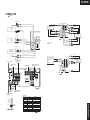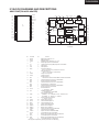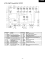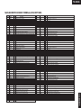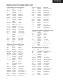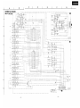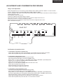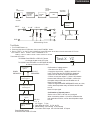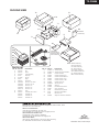
1
TX-DS595/696 Ref. No. 3678 042001 SERVICE MANUAL AUDIO VIDEO CONTROL RECEIVER MODEL TX-DS696 ZONE 2 REC OUT ZONE 2 LEVEL AUDIO VIDEO CONTROL RECEIVER MODEL TX-DS595 A SPEAKERS B CH LEVEL CH LEVEL STANDBY/ON DSP / MODE ADJ DSP / MODE ADJ SETUP RETURN RETURN POWER POWER PUSH TO ENTER PUSH TO ENTER ON OFF DISPLAY DIMMER FM MODE PRESET MEMORY TUNING PRESET AUDIO SELECTOR OFF DISPLAY SMART SCAN NAVIGATOR BASS PHONES SETUP STANDBY STANDBY ON MASTER VOLUME MASTER VOLUME STANDBY/ON VIDEO 1 VIDEO 2 VCR 1 VCR 2 VIDEO 3 VIDEO 4 TAPE FM AM PHONO CD DVD VIDEO 1 TUNING PRESET SMART SCAN NAVIGATOR BASS AUDIO SELECTOR VIDEO 2 VIDEO 3 TAPE FM AM PHONO TREBLE CD VCR AV RECEIVER TX-DS696 Black, Golden and Silver models BMDD BMPP,SMPP BMPA,GMPA BMWT,GMWT GMWR FM MODE PRESET MEMORY TREBLE PHONES DVD RT / PTY/ TP 120V AC, 60Hz 230-240V AC, 50Hz 220-230V/120V AC, 50/60 Hz SAFETY-RELATED COMPONENT WARNING!! COMPONENTS IDENTIFIED BY MARK ! ON THE SCHEMATIC DIAGRAM AND IN THE PARTS LIST ARE CRITICAL FOR RISK OF FIRE AND ELECTRIC SHOCK. REPLACE THESE COMPONENTS WITH ONKYO PARTS WHOSE PART NUMBER APPEAR AS SHOWN IN THIS MANUAL. MAKE LEAKAGE CURRENT OR RESISTANCE MEASUREMENTS TO DETERMINE THAT EXPOSED PARTS ARE ACCEPTABLY INSULATED FROM THE SUPPLY CIRCUIT BEFORE RETURNING THE APPLIANCE TO THE CUSTOMER. AV RECEIVER TX-DS595 Black, Golden and Silver models BMDD BMPP,SMPP BMPA,GMPA BMWT,GMWT GMWR 120V AC, 60Hz GMGT 220-230V AC,50 Hz 230-240V AC, 50Hz 220-230V/120V AC, 50/60 Hz TABLE OF CONTENTS Specifications TX-DS595 Specifications TX-DS696 Service procedures Panel views TX-DS595 Panel views TX-DS696 IC block diagrams and descriptions Microprocessor TX-DS595 Main microprocessor Sub microprocessor Microprocessor TX-DS696 Main microprocessor Sub microprocessor About debug mode FL tube view Printed circuit board-parts list TX-DS595 Printed cirucit board-parts list TX-DS696 Wiring view TX-DS595 Block diagram TX-DS595 Wirng view TX-DS696 Block diagram TX-DS696 Schematic diagrams & PC board views Input section TX-DS595 Input section TX-DS696 Power amplifier section 1 Power amplifier section 2 Display section TX-DS595 Display section TX-DS696 Video section TX-DS595 Video section TX-DS696 DSP section Adjustments and confirmation procedures Exploded view & Parts list TX-DS595 Exploded view & Parts list TX-DS696 Packing view TX-DS595 Packing view TX-DS696 2 3 4 5 8 11 20 20 22 24 24 26 27 28 29 34 39 41 43 45 47 47 51 55 59 63 67 71 75 81 87 89 93 97 98 TX-DS595 SPECIFICATIONS AMPLIFIER SECTION Continuous Average Power output (FTC) All channels: 75 W per channel min. RMS at 8 ohm , 2 channels driven from 20Hz to 20 kHz with no more than 0.08% total harmonic distortion. 100 W min. RMS at 6 ohm, 2 channels driven from 1 kHz with no more than 0.1% total harmonic distortion. Continuous Power output (DIN) 110 W at 6 ohm Maximum Power output (EIAJ) 140 W at 6 ohm Dynamic Power Output (Stereo) 2 210 W at 3 ohm 2 155 W at 4 ohm 2 90 W at 8 ohm Total Harmonic Distortion: 0.08% at rated power 0.08% at 1 W output IM Distortion: 0.08% at rated power 0.08% at 1 W output Damping Factor: 60 at 8 ohm Input Sensitivity and Impedance PHONO: 2.5 mV, 50 k ohm LINE (CD, TAPE, DVD, VIDEO 1,2,3): 200 mV, 50 k ohm MULTICHANNEL INPUT (FRONT L/C/R, SURROUND L/R): 200 mV, 50 k ohm (SUBWOOFER): 36 mV, 50 k ohm COAXIAL 1, 2 (DIGITAL): 0.5 Vp-p, 75ohm DVD, VIDEO1,2,3: 1 Vp-p, 75 ohm 1 Vp-p, 75 ohm (Y) 0.28 Vp-p, 75ohm (C) Output Level and Impedance Rec out (TAPE, VIDEO 1): 200 mV, 2.2 k ohm Pre out: 1 V, 470 ohm VIDEO (VIDEO 1, MONITOR OUT): 1 Vp-p, 75 ohm 1 Vp-p, 75 ohm (Y) 0.28 Vp-p, 75 ohm (C) Phono Overload: Frequency Response: RIAA Deviation: Tone Control Bass: Treble: Signal-to-Noise Ratio (Stereo) Phono: CD/Tape: Muting: TUNER SECTION FM Tuning Range: Usable Sensitivity Mono: 87.5 to 108.0 MHz (50-kHz steps) 11.2 dBf, 1.0 µV (75 ohm IHF) 0.9 µV (75 ohm DIN) 17.2 dBf, 2.0 µV (75 ohm IHF) 23 µV (75 ohm DIN) Stereo: 50 dB Quieting Sensitivity Mono: Stereo: Capture Ratio: Image Rejection Ratio: USA & Canadian models: Other area models: IF Rejection Ratio: Signal-to-Noise Ratio Mono: Stereo: Alternate Channel Attenuation: Selectivity: AM Suppression Ratio: Total Harmonic Distortion Mono: Stereo: Frequency Response: Stereo Separation: AM Tuning Range USA & Canadian models: European & Australian models: Worldwide models: Usable Sensitivity: Image Rejection Ratio: IF Rejection Ratio: Signal-to-Noise Ratio: Total Harmonic Distortion: GENERAL Power Supply: 180 mV RMS at 1 kHz, 0.5% T.H.D. 10 Hz to 100 kHz: +1 dB, - 3 dB 20 Hz to 20 kHz : ±0.8 dB ±10 dB at 50 Hz ±10 dB at 20 kHz 80 dB (IHF A, 5 mV input) 100 dB (IHF A, 0.5 V input) 50 dB Power Consumption: Dimensions (W H D): Weight: REMOTE CONTROLLER Transmitter: Signal range: Power supply: 17.2 dBf, 2.0 µV (75 ohm ) 37.2 dBf, 20 µV (75 ohm ) 2.0 dB 40 dB 85 dB 90 dB 76 dB 70 dB 55 dB 50 dB (DIN) 50 dB 0.2% 0.3% 30 Hz to 15 kHz, ±1.0 dB 45 dB at 1 kHz 30 dB at 100 Hz to 10 kHz 530 to 1,710 kHz (10-kHz steps) 522 to 1,611 kHz (9-kHz steps) 531 to 1,602 kHz (9-kHz steps) 530 to 1,710 kHz (10-kHz steps) 30 µV 40 dB 40 dB 40 dB 0.7% AC 120 V, 60 Hz (USA & Canadian models) AC 230-240 V, 50 Hz (European & Australian models) AC 220-230 and 120 V switchable, 50/60 Hz (Worldwide models) 4.7 A 380 W 435 175 431 mm 17-1/8" 6-7/8" 16-15/16" 25.4 lbs. (USA & Canadian models) 12.5 kg (Other models) Infrared Approx. 5 meters, 16 ft. Two " AA " batteries (1.5 V 2) Specifications and features are subject to change without notice. Power supply and voltage vary depending on the area in which the unit is purchased. TX-DS696 SPECIFICATIONS AMPLIFIER SECTION Continuous Average Power output (FTC) All channels: 100 W per channel min. RMS at 8 ohm , 2 channels driven from 20Hz to 20 kHz with no more than 0.08% total harmonic distortion. 125 W min. RMS at 6 ohm, 2 channels driven from 1 kHz with no more than 0.1% total harmonic distortion. Continuous Power output (DIN) 130 W at 6 ohm Maximum Power output (EIAJ) 160 W at 6 ohm Dynamic Power Output (Stereo) 2 230 W at 3 ohm 2 170 W at 4 ohm 2 115 W at 8 ohm Total Harmonic Distortion: 0.08% at rated power 0.08% at 1 W output IM Distortion: 0.08% at rated power 0.08% at 1 W output Damping Factor: 60 at 8 ohm Input Sensitivity and Impedance PHONO: 2.5 mV, 50 k ohm LINE (CD, TAPE, DVD, VIDEO 1-4): 200 mV, 50 k ohm MULTICHANNEL INPUT (FRONT L/C/R, SURROUND L/R): 200 mV, 50 k ohm (SUBWOOFER): 36 mV, 50 k ohm COAXIAL 1, 2 (DIGITAL): 0.5 Vp-p, 75ohm DVD, VIDEO1-4: 1 Vp-p, 75 ohm 1 Vp-p, 75 ohm (Y) 0.28 Vp-p, 75ohm (C) COMPONENT VIDEO 1, 2: 1 Vp-p, 75 ohm (Y) 0.7 Vp-p, 75ohm (CB /CR, PB /PR ) Output Level and Impedance Rec out (TAPE, VIDEO 1, 2): 200 mV, 2.2 k ohm Pre out: 1 V, 470 ohm VIDEO (VIDEO 1, 2, MONITOR OUT): 1 Vp-p, 75 ohm 1 Vp-p, 75 ohm (Y) 0.28 Vp-p, 75 ohm (C) COMPONENT VIDEO OUT: 1 Vp-p, 75 ohm (Y) 0.7 Vp-p, 75 ohm (CB /CR, PB /PR) 110 mV RMS at 1 kHz, 0.5% T.H.D. Phono Overload: Frequency Response: 5 Hz to 100 kHz: +1 dB, -3 dB RIAA Deviation: 20 Hz to 20 kHz : ±0.8 dB Tone Control Bass: ±10 dB at 50 Hz Treble: ±10 dB at 20 kHz Signal-to-Noise Ratio (Stereo) Phono: 80 dB (IHF A, 5 mV input) CD/Tape: 100 dB (IHF A, 0.5 V input) Muting: 50 dB TUNER SECTION FM Tuning Range: Usable Sensitivity Mono: 87.5 to 108.0 MHz (50-kHz steps) 11.2 dBf, 1.0 µV (75 ohm IHF) 0.9 µV (75 ohm DIN) 17.2 dBf, 2.0 µV (75 ohm IHF) 23 µV (75 ohm DIN) Stereo: 50 dB Quieting Sensitivity Mono: Stereo: Capture Ratio: Image Rejection Ratio: USA & Canadian models: Other area models: IF Rejection Ratio: Signal-to-Noise Ratio Mono: Stereo: Alternate Channel Attenuation: Selectivity: AM Suppression Ratio: Total Harmonic Distortion Mono: Stereo: Frequency Response: Stereo Separation: AM Tuning Range USA & Canadian models: European & Australian models: Worldwide models: Usable Sensitivity: Image Rejection Ratio: IF Rejection Ratio: Signal-to-Noise Ratio: Total Harmonic Distortion: GENERAL Power Supply: Power Consumption: Dimensions (W H D): Weight: REMOTE CONTROLLER Transmitter: Signal range: Power supply: 17.2 dBf, 2.0 µV (75 ohm ) 37.2 dBf, 20 µV (75 ohm ) 2.0 dB 40 dB 85 dB 90 dB 76 dB 70 dB 55 dB 50 dB (DIN) 50 dB 0.2% 0.3% 30 Hz to 15 kHz, ±1.0 dB 45 dB at 1 kHz 30 dB at 100 Hz to 10 kHz 530 to 1,710 kHz (10-kHz steps) 522 to 1,611 kHz (9-kHz steps) 531 to 1,602 kHz (9-kHz steps) 530 to 1,710 kHz (10-kHz steps) 30 µV 40 dB 40 dB 40 dB 0.7% AC 120 V, 60 Hz (USA & Canadian models) AC 230-240 V, 50 Hz (European & Australian models) AC 220-230 and 120 V switchable, 50/60 Hz (Worldwide models) 5.7 A 460 W 435 175 431 mm 17-1/8" 6-7/8" 16-15/16" 27.8 lbs. (USA & Canadian models) 13.5 kg (Other models) Infrared Approx. 5 meters, 16 ft. Two " AA " batteries (1.5 V 2) Specifications and features are subject to change without notice. Power supply and voltage vary depending on the area in which the unit is purchased. TX-DS595/696 SERVICE PROCEDURES 1. Replacing the fuses 5.Setting the AM tuning step frequency This symbol located near the fuses indicates that the fuse used is fast operating type. For continued protection against fire hazard, replace with same type fuse. For fuse rating refer to the marking adjacent to the symbol. Ce symbole indique que le fusible utlise est a rapide. Pour une protection permanente, n'untiliser que fusibles de meme type. Ce darnier est la qu le present symbol est appse. TX-DS696 CIRCUIT NO. F901 F902 F903 F9501 PART NO. 252198 252077 252075 252160 252075 DESCRIPTION 8A-UL,Fuse <D/WT/WR> 4A-SE-EAK,Fuse <P/WT/WR/A> 2.5A-SE-EAK,Fuse <P/A> 2.5A-UL/T-237,Fuse <D> 2.5A-SE-EAK,Fuse <P/A/WR/WT> PART NO. 252166 252076 252075 252160 252075 DESCRIPTION 6.3A-UL/T237,Fuse <D/WT/WR> 3.15A-SE-EAK,Fuse <P/WT/WR/A/GT> 2.5A-SE-EAK,Fuse <P/A> 2.5A-UL/T-237,Fuse <D> 2.5A-SE-EAK,Fuse <P/A/WR/WT/GT> (Wolrdwide models only) The initializing setting is 9 kHz, and this needs only to be changed if you are using the unit in a 10-kHz region. 1. Press the SETUP button. Turn the jog dial or press the and cursor buttons on the remote controller to display "3. PREFERENCE." 2. Press the jog dial or ENTER button on the remote controller. Turn the jog dial or press the cursor buttons on the remote controller to display "AM FREQ STEP?". 3.Press the jog dial or ENTER button on the remote controller. The currently set frequency step appears. 4.Turn the jog dial or press the and cursor buttons on the remote controller to set the frequency. 5. Press the RETURN button. "AM FREQ STEP?" appears in the FL tube. To exit the setup mode immediately, press the SETUP button. TX-DS595 CIRCUIT NO. F901 F902 F903 F9501 Note: <D>:120V model only <P>: European model only <WT>: Worldwide model only <WR>: Asian model only for 230V <GT>: 220-230V model only <A>: Australian model only 2. To initialize the unit This device employs a microprocessor to perform various functions and operations. If interference generated by an external power supply, radio wave, or other electrical source results in accident which causes the specified operations and functions to operate abnormally. To perform a result, please follow the procedure below. 1.Turn POWER to on. 2.Press and hold down the PRESET MEMORY button, then press the STANDBY button. After "clear" is displayed, the preset memory and each mode stored in the memory, such as surround, are initialized and will return to the factory setting. 3.Disconnect Power supply cord. 6.Setting the Voltage selector (Worldwide models only) Worldwide models are equipped with a voltage selector to conform with local power supplies. Be sure to set this switch to match the voltage of the power supply in your area before plugging in the unit. 1. Determine the proper voltage for your area: 220-230 V or 120 V. 2. If the preset voltage is not correct for your area, insert a screwdriver into the groove in the switch. Slide the switch all the way to the right (120 V) or to the left (220-230 V), whichever is appropriate. FRONT SPEAKERS COMPONENT VIDEO ANTENNA Y PB PR Y OUT IN PB PR Y IN IN PR PB INPUT 1 OUTPUT IN OUT SURROUND SPEAKERS L R INPUT 2 AC OUTLET SWITCHED 100W MAX. IN VIDEO MONITOR OUT FM 75 DVD VIDEO 1 VIDEO 2 REMOTE CONTROL VIDEO 3 VIDEO 4 S VIDEO VOLTAGE SELECTOR AV RECEIVER PHONO CD OUT TAPE : TX-DS696 MODEL NO. / IN L L R R R CAUTION: PRE OUT FRONT FRONT L SURR CENTER OPTICAL 1 1 2 R SUBWOOFER MULTI CHANNEL INPUT SURR CENTER L R SUB WOOFER ZONE 2 SPEAKERS VOLTAGE SELECTOR L SEE INSTRUCTION MANUAL FOR CORRECT SETTING. COAXIAL 2 GND PRE OUT 120V 1 120V 2 6 OHMS MIN. / SPEAKER 4 OHMS MIN. / SPEAKER 220-230V SET BEFORE POWER ON IMPEDANCE SELECTOR DIGITAL INPUT 3. Safety-check out (Only U.S.A. model) After correcting the original service problem, perform the following safety check before releasing the set to the customer. Connect the insulating-resistance tester between the plug of power supply cord and screw on the back panel. Specifications: 3.3Mohm+/-10% at 500V. 4. Memory Preservation This unit does not require memory preserv ation batteries. A built-in memory po wer back-up system preserv es the contents of the memory during po wer f ailures and even when the unit is unplugged. The unit must be plugged in order to char ge the back-up system. The memory preserv ation period after the unit has been unplugged v aries depending on climate and placement of the unit. On the a verage, memory contents are protected over a period of a fe w weeks after the last time the unit has been unplugged. This period is shorter when the unit is e xposed to a highly humid climate. CENTER SPEAKER L R AM 220-230V 7. Changing the AM band step With the exception of the worldwide models,a tuning step step setup mode is not provided. When you change the band step, change the parts as shown below. R7780,R7781 R7880,R7881 To 10kHz 330 ohm Open To 9kHz Open 2.2 kohm TX-DS595 PANEL VIEWS SMART SCAN NAVIGATOR jog dial and indicators Front panel See illustration below A SPEAKERS B CH LEVEL MASTER VOLUME Used to make settings in the setup display, change listening mode settings, and more. STANDBY indicator Lights when the TX-DS595 is in the standby state and flashes when a signal is received from the remote controller. SETUP button Press to enter and exit the setup mode. STANDBY/ON button Press to turn on the TX-DS595 when in the standby state. Press again to return the TX-DS595 to the standby state. STANDBY/ON DSP / MODE ADJ POWER switch Turns on and off the main power supply for the TX-DS595. SETUP STANDBY RETURN POWER SPEAKERS A/B buttons Press these buttons to turn on and off speakers systems A and B. PUSH TO ENTER ON OFF DISPLAY RT / PTY/ TP FM MODE PRESET MEMORY DVD VIDEO 1 TUNING PRESET SMART SCAN NAVIGATOR BASS PHONES AUDIO SELECTOR VIDEO 2 VIDEO 3 FM TAPE AM PHONO CH LEVEL button Press to select the channel whose level is to be adjusted. VCR AV RECEIVER TX-DS595 MASTER VOLUME dial The MASTER VOLUME dial is used to control the volume. PHONES jack To listen with headphones, plug a pair headphones with a standard stereo plug into the PHONES jack on the TX-DS595 front panel. When you connect headphones, the unit will enter STEREO mode automatically and no sound will be heard from the speakers. If you have selected MULTI CH INPUT, you will hear sound only from the FRONT L and R channels. Note that the volume level for the headphones is adjustable. For all models other than European model SETUP PHONES DIMMER DISPLAY RT / PTY/ TP FM MODE PRESET MEMORY TUNING PRESET SMART SCAN NAVIGATOR AUDIO SELECTOR button This button is used to select the type of audio input signal. Each time pressed, the setting cycles from “AUTO” “MULTICH” “ANALOG” and back. Input source buttons (DVD, VIDEO 1–3, TAPE, FM, AM, PHONO, and CD) These buttons are used to select the input source. Front panel display Speakers A/B indicators Listening mode or digital input format indicators Tuning indicators BASS dial Boosts or cuts the bass response. Bass adjustment is effective only for the front speakers and headphones. SPEAKERS A B RT/PTY/TP (European models only) button This button is only available on European models. Use this button to help tune into the Radio Data System (RDS) for FM broadcasting. RDS was developed within the European Broadcasting Union (EBU) and is available in most European countries. Each time the button is pressed, the display changes from RT (radio text) to PTY (program type) to TP (traffic program) and then back to RT again. DIMMER (other than European models) button Press to set the brightness of the front display. There are 3 settings available: normal, dark, and very dark. FM MODE button When there is too much noise in the stereo reception of an FM broadcast, press to turn off the FM MUTE function. RETURN PUSH TO ENTER DISPLAY DISPLAY button The DISPLAY button is used to display information about the current input source signal. Each time you press the display button, the screen changes to show you different information concerning the input signal. TREBLE CD DSP / MODE ADJ RETURN button Press to move up one level in the setup mode. SLEEP MPEG DTS DSP PC M DIGITAL STEREO TUNED FM MUTE DIRECT FM STEREO MEMORY RDS ft ch dB TREBLE dial Boosts or cuts the treble response. Treble adjustment is effective only for the front speakers and headphones. PRESET MEMORY button This button is used to assign the radio station that is currently tuned in to a preset channel or delete a previously preset station. TUNING / buttons Use these buttons to change the tuner frequency. The tuner frequency is displayed in the front display and it can be changed in 50 kHz increments for FM and 10 kHz (or 9 kHz) increments for AM. When FM is selected, you can hold down one of the tuning buttons and then release it to activate the auto-search feature. It will search for a station in the direction of the button you pressed and stop when it tunes into one. PRESET / buttons When AM or FM is selected as the input source, press one of these buttons to jump to a radio station that you preset using the PRESET MEMORY button. Pressing the right button moves from the most recently preset station to older ones, and pressing the left button moves in the reverse order. Multi function display Remote control sensor 7 TX-DS595 Front display Sleep indicator TX-DS595 REMOTE CONTROLLER SEND/LEARN indicator This indicator acts as a guide when commands are programmed into or sent by the remote controller. It also warns the user when an error is made or battery power is low. SEND / LEARN PR EP E S LE RO G RA M MED & LEARNING CAPA BILITY STDBY ON P MACRO DIR EC T R MO DE MODE MD R CV CABL VCR E TV T SA RE TU R SET UP N CH DISC VOL C TO H S E PM L ENU AUDIO ON/STDBY button ON: Turns on the TX-DS595. STDBY: Places the TX-DS595 in the standby state. Be aware that pressing the STDBY button only places the TXDS595 in standby and does not turn the power completely off. DVD CD T TES U MEN MUTING SUBTITLE ANGLE TV / VCR LEVEL RANDOM SLEEP button Sets the sleep function. The SLEEP button enables you to set the TX-DS595 to turn off automatically after a specified time period. DIRECT MACRO button For executing and programming the Direct Macro function. MODE buttons and indicators For selecting the component to be operated by the remote controller. When a MODE button is pressed, it will light green for 8 seconds. The selected MODE button will also light whenever any other operation button is pressed to tell you which mode the remote controller is in. OPEN / CLOSE RETURN button Press to move up one level in the setup mode. REC INPUT SELECTOR DVD CD V1 V3 V4 TUN STEREO DIRECT 1 2 SURR T2 T1 V2 A.ST PH DSP CH/DISC button When in the RCVR mode, for selecting a tuner preset channel. For selecting the disc to be played back for components with disc changers when in the DVD or CD modes. Numeric key/Listening mode selector/SP A, B/ Re-EQ/DISPLAY/DIMMER buttons 1 to 9, +10, --/---, 0: For entering the number of a track. STEREO, DIRECT, DSP / , SURR, A.ST: You can select a listening mode. STEREO: Changes the listening mode directly to the Stereo listening mode. If pressed, the listening mode for the selected input source set in the Listening Mode Preset is also changed to the Stereo listening mode. SURR (Surround): Changes the listening mode to the surround mode for the current input signal (e.g., Dolby Pro Logic II, Dolby Digital, or DTS). If pressed, the listening mode for the selected input source set in the Listening Mode Preset is also changed to the Surround listening mode. For Dolby Pro Logic II, this button also changes the mode between Dolby Pro Logic II Movie and Dolby Pro Logic II Music. DIRECT: Changes the listening mode directly to the Direct listening mode. If pressed, the listening mode for the selected input source set in the Listening Mode Preset is also changed to the Direct listening mode. A.ST (All Channel Stereo): Changes the listening mode directly to the Stereo listening mode. If pressed, the listening mode for the selected input source set in the Listening Mode Preset is also changed to the All Channel Stereo listening mode. DSP / : Changes the listening mode as shown below. Direct Stereo Surround Orchestra Unplugged Studio-Mix TV Logic All Ch Stereo Direct. If pressed, the listening mode for the selected input source set in the Listening Mode Preset is also changed. TEST/MENU button TEST: Outputs a test tone for setting speaker levels. Use this button in conjunction with the LEVEL / and CH SEL buttons to calibrate the speakers levels. 1. Press the TEST button. A test sound (pink noise) will be heard from the left front speaker. At this point, it is not necessary to adjust the volume of the test sound. 2. Press the CH SEL button. The test sound will now be heard from a different speaker. 3. Use the LEVEL / buttons to adjust the volume of the test sound from this speaker to the same level that you heard from the previous speaker. 4. Repeat the procedure in step 2 and 3 until the volume of the test sound from all speakers is the same level. Each time you press the CH SEL button, the test sound will be heard from a different speaker. The speaker order for calibration is front left center front right surround right surround left subwoofer. 5. Press the TEST button to exit the setting. MENU: When in the DVD mode, this button displays the DVD menu. MUTING button Activates the mute function. ZONE 2/SEARCH/ENTER button ZONE 2: Not used with the TX-DS595. SEARCH: When in the DVD mode, for finding the specific section on a disc where you want to start playback. ENTER: When in the MD mode, for confirming the selection. 3 DSP 4 5 6 SP A SP B Re-EQ 7 8 9 DISPLAY DIMMER ZONE 2 +10 0 SEARCH -- / --- Selects an input source. Same as the input selector buttons on front panel of the TX-DS595. The input source for each buttons is given here. DVD:DVD, CD:CD, V1:VIDEO1, V2:VIDEO2, V3:VIDEO3, V4:Not used with the TXDS595, T1:TAPE, T2:Not used with the TX-DS595, TUN:FM/AM, PH:PHONO. ENTER HOME THEATER CONTROLLER RC-447M CH SEL/TOP MENU button CH SEL: For selecting the speaker for level adjustment when in the RCVR mode. Used together with the LEVEL / buttons. TOP MENU: When in the DVD mode, for displaying the menu screen(s) recorded on DVD media. AUDIO/TV/VCR button AUDIO: For selecting the audio input signal. The setting changes from “AUTO” to “MULTICH” to “ANALOG” and back each time this button is pressed. TV/VCR: Must be preprogrammed for use in the TV and VCR modes. LEVEL /ANGLE and LEVEL /SUBTITLE buttons LEVEL / : Select the speaker whose volume is to be adjusted using the CH SEL button and adjust the volume using the LEVEL / buttons in the RCVR mode. ANGLE: When in the DVD mode, for selecting a camera angle when a DVD-Video is recorded with multiple angle playback. SUBTITLE: When in the DVD mode, for selecting one of the subtitle languages recorded on a DVD-Video. INPUT SELECTOR buttons SP A, SP B: For turning on and off speakers systems A and B. DISPLAY: For changing the display in the front display. DIMMER: Adjusts the display brightness. There are three settings available: normal, dark and very dark. MODE MACRO button For executing and programming the Macro function. SETUP button Press to enter and exit the setup mode. ENTER/cursor button For selecting and entering settings in the setup mode. VOL button For adjusting the volume. 7 9 TX-DS595 CD/TAPE/DVD/MD operation buttons For operating Onkyo components connected to the TX-DS595. Re-EQ: Depending on the listening mode, you can turn the cinema re-equalization function on or off. Re-EQ (re-equalization) takes the edginess or “brightness” out of your home cinema sound to compensate for the fact that sound mixed for theaters may sound too bright when played back through speakers in the home environment. On: Select to turn on the re-equalization filter. Off: Select to turn off the re-equalization filter. Note: The Re-EQ function is effective on the Dolby Pro Logic II Movie and Dolby Digital modes. TX-DS595 CONNECTION : Signal flow Analog audio output L (White) MONITOR OUT VIDEO 1 DVD IN Video output VIDEO 2 VIDEO 3 V IN IN IN OUT VIDEO VIDEO S video R (Red) REMOTE CONTROL 4. DVD player (DVD) NO 2. CD player (CD) CD TAPE OUT Analog audio output R R R (Red) L (White) FRONT ANTENNA Digital audio output (optical) L SURR CENTER OPTICAL 1 COAXIAL 2 1 Digital audio output (Coaxial) Analog audio output AM MONITOR OUT Analog audio output VIDEO 1 DVD IN IN IN OUT R (Red) VIDEO 2 VIDEO S video output L (White) IN L S video output Video output S VIDEO S VIDEO IN 2 R ER Digital audio output (Coaxial) UT MULTI CHANNEL INPUT 5. VCR (VIDEO 1) SUB WOOFER DIGITAL INPUT FM 75 L (White) REMOTE CONTROL Video input 1. Turntable (PHONO) PHONO R (Red) CD OUT TAPE IN L S video input R R (Red) : Signal flow FRONT Ground wire (earth) L SURR CENTER OPTICAL 1 COAXIAL 2 Analog audio input 1 GND L (White) 2 R Analog audio input SUBWOOFER PRE OUT MULTI CHANNEL INPUT SUB WOOFER DIGITAL INPUT L (White) 3. Tape deck, MD recorder, DAT deck, CD recorder, (TAPE) R (Red) L (White) Video output S video output R (Red) 7. TV monitor or Projector (MONITOR OUT) Analog audio output Connecting your video components Connecting antennas MONITOR OUT Video input S video input CD OUT IN 6. Satelite tuner, or settop box (VIDEO 2 / VIDEO 3) R (Red) IN Analog audio output L SURR CENTER OPTICAL 1 COAXIAL 2 1 2 VIDEO 2 VIDEO 3 IN TAPE R ER IN OUT L (White) R UT VIDEO 1 DVD IN L L R AM MONITOR OUT IN S VIDEO SURROUND SPEAKERS CENTER SPEAKER L R VIDEO 2 VIDEO 3 IN REMOTE CONTROL FRONT FRONT SPEAKERS A OUT Cautions regarding the AC OUTLETS connectors Connecting speakers ANTENNA IN VIDEO NO Connect to devices with terminals VIDEO 1 DVD MULTI CHANNEL INPUT SUB WOOFER DIGITAL INPUT Digital audio output (optical) TV, IN VIDEO FM 75 REMOTE CONTROL PHONO CD OUT S VIDEO TAPE FRONT SPEAKERS B IN L L AV RECEIVER R R AC OUTLETS L R MODEL NO. TX-DS595 AC 230-240 V 50 Hz SWITCHED TOTAL 100W MAX. CAUTION: FRONT L SURR CENTER OPTICAL 1 SEE INSTRUCTION MANUAL FOR CORRECT SETTING. COAXIAL 2 GND 1 6 OHMS MIN. / SPEAKER 4 OHMS MIN. / SPEAKER 2 R SUBWOOFER PRE OUT MULTI CHANNEL INPUT Connecting a subwoofer SET BEFORE POWER ON SUB WOOFER IMPEDANCE SELECTOR DIGITAL INPUT Connect to devices with multichannel output Connecting your audio components 120V 220-230V Voltage selector For worldwide models only Digital input COAX 1 COAX 2 ---OPT 2 ------- Multichannel Yes No No No No No ---OPT 1 No No COAX: Coaxial OPT: Optical ----: No setting : Not applicable TX-DS595 VOLTAGE SELECTOR Default setting Input source DVD VIDEO 1 VIDEO 2 VIDEO 3 VIDEO 4 TAPE FM AM PHONO CD TX-DS696 PANEL VIEWS Remote control sensor Front panel POWER switch Turns on and off the main power supply for the TX-DS696. See illustration below STANDBY indicator Lights when the TX-DS696 is in the standby state and flashes when a signal is received from the remote controller. ZONE 2 REC OUT ZONE 2 LEVEL CH LEVEL MASTER VOLUME STANDBY/ON button Press to turn on the TX-DS696 when in the standby state. Press again to return the TX-DS696 to the standby state. STANDBY/ON DSP / MODE ADJ SETUP STANDBY RETURN POWER PUSH TO ENTER ON OFF DISPLAY DIMMER FM MODE PRESET MEMORY TUNING PRESET SMART SCAN NAVIGATOR BASS PHONES AUDIO SELECTOR DVD VIDEO 1 VIDEO 2 VCR 1 VCR 2 VIDEO 3 VIDEO 4 TAPE FM AM PHONO TREBLE REC OUT button Press the REC OUT button to output the audio signals to a recording component for recording purposes. CD AV RECEIVER TX-DS696 ZONE 2 button and indicator Press the ZONE 2 button to enjoy the output from the TX-DS696 in a different room, which is referred to as a remote zone (Zone 2). ZONE 2 indicator lights when a signal is output to the remote zone (Zone 2). When the ZONE 2 indicator is off, then either output to the remote zone is turned off or Rec Out is selected. ZONE 2 LEVEL button Press to enter the mode for adjusting the volume in the remote zone (Zone 2). For European model DSP / MODE ADJ SETUP CH LEVEL button Press to select the channel whose level is to be adjusted. RETURN PUSH TO ENTER DISPLAY RT/PTY/TP DISPLAY DIMMER FM MODE PRESET MEMORY TUNING PRESET SMART SCAN NAVIGATOR MASTER VOLUME dial The MASTER VOLUME dial is used to control the volume for the main zone. The volume for the remote zone (Zone 2) is independent. PHONES jack This is a standard stereo jack for connecting stereo headphones. AUDIO SELECTOR button This button is used to select the type of audio input signal. Each time pressed, the setting cycles from “AUTO” “Multich” “Analog” and back. Front panel display Rec out indicator Sleep indicator Listening mode or digital input format indicators Tuning indicators Input source buttons (DVD, VIDEO 1–4, TAPE, FM, AM, PHONO, and CD) These buttons are used to select the input source for the main zone. To select the input source for the remote zone (Zone 2) or recording out (Rec Out), first press the Zone 2 or Rec Out button, and then the desired input source button. BASS dial Boosts or cuts the bass response. Bass adjustment is effective only for the front speakers and headphones. Zone 2 indicator Multi fanction display Front display Used to make settings in the Setup menu, change listening mode settings, and more. SETUP button Press to bring up the Setup menu. The OSD menu will appear on the TV monitor as well as the front display on the TX-DS696. RETURN button Press to exit the Main menu level or go back one level up. DISPLAY button The DISPLAY button is used to display information about the current input source signal. Each time you press the display button, the screen changes to show you different information concerning the input signal. RT/PTY/TP (European models only) button This button is only available on European models. Use this button to help tune into the Radio Data System (RDS) for FM broadcasting. RDS was developed within the European Broadcasting Union (EBU) and is available in most European countries. Each time the button is pressed, the display changes from RT (radio text) to PTY (program type) to TP (traffic program) and then back to RT again. DIMMER (other than European models) button [30] Press to set the brightness of the front display. There are 3 settings available: normal, dark, and very dark. FM MODE button If you are listening to an FM radio station in stereo and the sound cuts out or there is a great deal of noise, switch from STEREO to MONO. Each time this button is pressed, the AUTO indication flashes and the stereo mode changes from AUTO to MONO and vice versa. This button also turns on and off the FM MUTE. PRESET MEMORY button This button is used to assign the radio station that is currently tuned in to a preset channel or delete a previously preset station. TUNING / buttons Use these buttons to change the tuner frequency. The tuner frequency is displayed in the front display and it can be changed in 50 kHz increments for FM and 10 kHz (or 9 kHz) increments for AM. When FM is selected, you can hold down one of the tuning buttons and then release it to activate the auto-search feature. It will search for a station in the direction of the button you pressed and stop when it tunes into one. PRESET / buttons When AM or FM is selected as the input source, press one of these buttons to jump to a radio station that you preset using the PRESET MEMORY button. Pressing the right button moves from the most recently preset station to older ones, and pressing the left button moves in the reverse order. TX-DS696 TREBLE dial Boosts or cuts the treble response. Treble adjustment is effective only for the front speakers and headphones. SMART SCAN NAVIGATOR jog dial and indicators TX-DS696 REMOTE CONTROLLER SEND/LEARN indicator This indicator acts as a guide when commands are programmed into or sent by the remote controller. It also warns the user when an error is made or battery power is low. ON/STDBY button ON: Turns on the TX-DS696. STDBY: Places the TX-DS696 in the standby state. Be aware that pressing the STDBY button only places the TXDS696 in standby and does not turn the power completely off. SLEEP button Sets the sleep function. The SLEEP button enables you to set the TX-DS696 to turn off automatically after a specified time period. DIRECT MACRO button For executing and programming the Direct Macro function. MODE buttons and indicators For selecting the component to be operated by the remote controller. When a MODE button is pressed, it will light green for 8 seconds. The selected MODE button will also light whenever any other operation button is pressed to tell you which mode the remote controller is in. RETURN button For entering the selected setting and returning to the previous menu. CH/DISC button When in the RCVR mode, for selecting a tuner preset channel. For selecting the disc to be played back for components with disc changers when in the DVD or CD modes. CH SEL/TOP MENU button CH SEL: For selecting the speaker for level adjustment when in the RCVR mode. Used together with the LEVEL / buttons. TOP MENU: When in the DVD mode, for displaying the menu screen(s) recorded on DVD media. HOME THEATER CONTROLLER RC-440M AUDIO/A/TV/VCR button AUDIO/A: For selecting the audio input signal. The setting changes from “AUTO” to “Multich” to “Analog” and back each time this button is pressed. TV/VCR: Must be preprogrammed for use in the TV and VCR modes. LEVEL /ANGLE and LEVEL /SUBTITLE buttons LEVEL / : Select the speaker whose volume is to be adjusted using the CH SEL button and adjust the volume using the LEVEL / buttons in the RCVR mode. ANGLE: When in the DVD mode, for selecting a camera angle when a DVD-Video is recorded with multiple angle playback. SUBTITLE: When in the DVD mode, for selecting one of the subtitle languages recorded on a DVD-Video. ZONE 2/SEARCH/ENTER button ZONE 2: When in the RCVR mode, press this button to perform operations on the remote zone (Zone 2). SEARCH: When in the DVD mode, for finding the specific section on a disc where you want to start playback. ENTER: When in the MD mode, for confirming the selection. Numeric key/Listening mode selector/SP A, B/ Re-EQ/DISPLAY/DIMMER buttons 1 to 9, +10, --/---, 0: For entering the number of a track. STEREO, DIRECT, DSP / , SURR, A.ST: You can select a listening mode. Re-EQ: Depending on the listening mode, you can turn the cinema re-equalization function on or off. SP A, SP B: Not used with the TX-DS696. DISPLAY: For changing the display in the front display. DIMMER: Adjusts the display brightness. There are three settings available: normal, dark and very dark. LIGHT button For illuminating the buttons of the remote controller. This is button is useful when using the remote controller in dark locations. When pressed, the buttons on the remote controller light green. The button for the mode currently selected lights brighter than the rest. MODE MACRO button For executing and programming the Macro function. SETUP button For displaying and quitting the Setup menu. ENTER/cursor button When selecting items in the Setup menu, press the upper and lower portions to select item, press the right and left portions to select parameter values or modes, and press ENTER to select item. VOL button For adjusting the volume. TEST/MENU button TEST: Outputs a test tone for setting speaker levels. Use this button in conjunction with the LEVEL / and CH SEL buttons to calibrate the speakers levels without entering the Setup menu. When TEST button is pressed, the test noise (pink noise) is output. Use the LEVEL / buttons to increase or decrease the sound level. Use the CH SEL button to change from speaker to speaker. MENU: When in the DVD mode, this button displays the DVD menu. MUTING/M button Activates the mute function. TX-DS696 CD/TAPE/DVD/MD operation buttons For operating Onkyo components connected to the TX-DS696. INPUT SELECTOR buttons Selects an input source. Same as the input selector buttons on front panel of the TX-DS696. The input source for each buttons is given here. DVD:DVD, CD:CD, V1:VIDEO1, V2:VIDEO2, V3:VIDEO3, V4:VIDEO4, T1:TAPE, T2:Not used with the TX-DS696, TUN:FM/AM, PH:PHONO. TX-DS696 CONNECTIONS Connecting your video components [14, 15] Connecting antennas Connect to devices with terminals Cautions regarding the AC OUTLETS connectors Connecting speakers CR/PR FRONT SPEAKERS COMPONENT VIDEO ANTENNA Y PB PR Y PB Y PR PB PR CENTER SPEAKER Y SURROUND SPEAKERS L R L R CB/PB CB/PB Component video output AM INPUT 1 OUTPUT IN OUT IN OUT Y INPUT 2 IN IN CB MONITOR OUT FM 75 DVD VIDEO 1 VIDEO 2 SWITCHED 100W MAX. CD OUT L R CAUTION: PRE OUT OPTICAL 1 CENTER L 1 IN INPUT 2 OUT VIDEO 1 IN IN VIDEO 2 V IN 6 OHMS MIN. / SPEAKER Video output L 220-230V S video output R (Red) CENTER OPTICAL 1 COAXIAL 2 1 Connecting power amplifiers Component video INPUT 1 INPUT 2 INPUT 1 INPUT 1 INPUT 1 Video input S video input : Signal flow R (Red) Analog audio input Multichannel Yes No No No No No L (White) Audio connection cable Left (White) Component video connection cable S video connection cable CR/PR CR/PR CB/PB CB/PB Y Y R Component video input No No Audio connection cable Video connection cable L Right (Red) CR/PR Video output CB/PB COAX: Coaxial OPT: Optical ----: No setting : Not applicable COMPONENT VIDEO 8. TV monitor or Projector (MONITOR OUT) Y CB CR Y OUT IN CB CR Y IN IN CB S video output IN INPUT 1 OUT INPUT 2 IN Video input Analog audio output VIDEO MONITOR OUT DVD VIDEO 1 VIDEO 2 S video input L (White) Video input L (White) VIDEO 3 VIDEO 4 9. Settop box or Video camera, etc. (VIDEO 4) S VIDEO TAPE R (Red) IN Analog audio output L S video input R (Red) CR Y OUTPUT : Signal flow 7. DVD recorder or other digital video recording device (VIDEO 1) DIGITAL INPUT UT Voltage selector Connecting the remote zone speakers ---OPT 1 2 SUB WOOFER Digital audio output (Coaxial) Digital input COAX 1 COAX 2 ---OPT 2 ------- Digital audio output (Coaxial) Analog audio output R (Red) Default setting Input source DVD VIDEO 1 VIDEO 2 VIDEO 3 VIDEO 4 TAPE FM AM PHONO CD Analog audio output R L (White) SET BEFORE POWER ON Connecting your audio components S video output L (White) IN 120V 4 OHMS MIN. / SPEAKER IMPEDANCE SELECTOR DIGITAL INPUT Connecting a subwoofer S video S VIDEO TAPE L SEE INSTRUCTION MANUAL FOR CORRECT SETTING. 2 SUB WOOFER Connect to devices with multichannel output VIDEO 3 VIDEO 4 1 R 2 R MULTI CHANNEL INPUT SURR COAXIAL 2 DVD 4. DVD player (DVD) VOLTAGE SELECTOR FRONT CENTER GND MONITOR OUT ZONE 2 SPEAKERS : TX-DS696 MODEL NO. / IN R PRE OUT CR VIDEO TAPE SURR INPUT 1 OUT IN Video output L L CB S VIDEO R FRONT Y CR CR/PR AV RECEIVER PHONO CB OUTPUT VIDEO 3 VIDEO 4 REMOTE CONTROL Y CR Y AC OUTLET IN VIDEO SUBWOOFER Component video output COMPONENT VIDEO Video output R L (White) CENTER Analog audio input 2. CD player (CD) 5. VCR (VIDEO 2) Digital audio output (optical) COMPONENT VIDEO ANTENNA Y PB PR Y OUT IN PB OPTICAL 1 R (Red) Video output 2 1 2 6. Satellite tuner or TV (VIDEO 3) SUB WOOFER UT PR S video output COAXIAL DIGITAL INPUT L (White) AM OUTPUT IN INPUT 1 OUT S video output IN R (Red) Analog audio output L (White) 1. Turntable (PHONO) MONITOR OUT FM 75 DVD VIDEO 1 Analog audio output R (Red) VIDEO 2 Analog audio output REMOTE CONTROL L (White) Digital audio output (optical) PHONO R (Red) CD OUT TAPE IN L R FRONT Ground wire (earth) L SURR CENTER OPTICAL 1 COAXIAL 2 GND 1 2 Analog audio input R SUBWOOFER PRE OUT MULTI CHANNEL INPUT SUB WOOFER DIGITAL INPUT L (White) R (Red) L (White) R (Red) Analog audio output TX-DS696 3. Tape deck, MD recorder, DAT deck, CD recorder, (TAPE) TX-DS595/696 IC BLOCK DIAGRAMS AND DESCRIPTIONS AK4112AVF(24-bit 96-kHz DIR) DVDD 1 28 CM0/CDTO DVSS 2 27 CM1/CDTI TVDD 3 26 OCKS1/CCLK V/TX 4 25 OCKS0/CSN RX1 MCKO1 RX2 RX3 XTI 24 5 23 MCKO2 22 DAUX 8 21 BICK AVDD 9 20 SDTO AVSS 10 19 LRCK XTO 6 PDN 7 R Top View AVSS AVDD Input R MCKO1 MCKO2 Clock Clock Recovery Generator XTI XTO X'tal Oscillator Selector RX4 96kHz Detect V/TX DAIF LRCK DEM RX1 11 18 ERF RX2/DIF0 12 17 FS96 RX3/DIF1 13 16 P/SN RX4/DIF2 14 15 AUTO FS96 DAUX DVDD Decoder Audio BICK I/F SDTO DVSS TVDD CSN System PDN Control AC-3/MPEG Detect Error µp I/F CCLK CDTO Detect CDTI AUTO ERF Serial mode No. 1 2 3 5 6 Pin Name DVDD DVSS TVDD V TX XTI XTO 7 PDN 8 R - 9 10 AVDD AVSS - 11 RX1 I DIF0 RX2 DIF1 RX3 DIF2 RX4 I I I I I I 15 AUTO O 16 P/S I 17 FS96 O 4 12 13 14 18 ERF 19 20 21 22 23 24 LRCK SDTO BICK DAUX MCK02 MCK01 OCKS0 CSN OCKS1 CCLK CM1 CDTI 25 26 27 28 CM0 I/O O O I O I O I/O O I/O I O O I I I I I I I Function Digital Power Supply Pin, 3.3V Digital Ground Pin Input Buffer Power Supply Pin, 3.3V or 5V Validity Flag Output Pin in Parallel Mode Transmit channel (through data) Output Pin in Serial Mode X'tal Input Pin X'tal Output Pin Power-Down Mode Pin When“ L”, the AK4112A is powered-down and reset. External Resistor Pin 18k W +/-1% resistor to AVSS externall y. Analog Power Supply Pin Analog Ground Pin Receiver Channel 1 This channel is selected in Parallel Mode or default of Serial Mode. Audio Data Interface Format 0 Pin in Parallel Mode Receiver Channel 2 in Serial Mode Audio Data Interface Format 1 Pin in Parallel Mode ReceiverChannel 3 in Serial Mode Audio Data Interface Format 2 Pin in Parallel Mode Receiver Channel 4 in Serial Mode Non-PCM Detect Pin “ L” : No detect,“ H” : Detect Parallel/Serial Select Pin “ L” : Serial Mode,“ H” : Parallel Mode 96kHz Sampling Detect Pin (RX Mode) “ H” : fs=88.2kHz or more, “ L” fs=54kHz or less. (X’ tal Mode) “ H” : XFS96=1,“ L” : XFS96=0. Unlock & Parity Error Output Pin “ L” : No Error,“ H” : Error Output Channel Clock Pin Audio Serial Data Output Pin Audio Serial Data Clock Pin Auxiliary Audio Data Input Pin Master Clock #2 Output Pin Master Clock #1 Output Pin Output Clock Select 0 Pin in Parallel Mode Chip Select Pin in Serial Mode Output Clock Select 1 Pin in Parallel Mode Control Data Clock Pin in Serial Mode Master Clock Operation Mode Pin0 in Parallel Mode Control Data Input Pin in Serial Mode Master Clock Operation Mode Pin1 in Parallel Mode CDTO O Control Data Output Pin in Serial Mode 1: All input pins except internal pull-down pins should not be left floating. P/S="L" TX-DS595/696 AK4527VQ(24bit 96kHz 6-ch. CODEC) LIN+ LIN- ADC HPF RIN+ RIN- ADC HPF DAC DATT LPF LOUT1 ROUT1 LPF DAC DATT LOUT2 LPF DAC DATT ROUT2 LPF DAC DATT LOUT3 LPF DAC DATT PIN/FUNCTION No. Pin Name I/O 1 SDOS I Audio I/F MCLK MCLK LRCK BICK LRCK BICK DAUX Format Converter SDOUT SDOS SDTO LPF ROUT3 DAC SDTI1 SDTI2 SDTI3 SDIN1 SDIN2 SDIN3 DATT AK4527 LOOP1 LOOP0/CDTI DF1/CCLK DIF0/CSN P/S MCLK DZF1 AVSS AVDD VREFH VCOM 44 43 42 41 40 39 38 37 36 35 34 Pin Layout SDOS 1 33 DZF2 12C 2 32 RIN+ SMUTE 3 31 RIN- BICK 4 30 LIN+ LRCK 5 29 LIN- SDTI1 6 28 ROUT1 SDTI2 7 27 LOUT1 SDYI3 8 26 ROUT2 SDTO 9 25 LOUT2 DAUX 10 24 ROUT3 DFS 11 23 LOUT3 AK4527VQ 22 CAD0 21 CAD1 20 ICKS0 19 ICKS1 18 ICKS2 17 PDN 16 DVSS 15 DVDD 14 TVDD 13 DEM0 DEM1 12 Top View 2 I2C I 3 SMUTE I 4 5 6 7 8 9 10 11 BICK LRCK SDTI1 SDTI2 SDTI3 SDTO DAUX DFS I I I I I O I I 12 13 14 15 16 17 DEM1 DEM0 TVDD DVDD DVSS PDN I I I 18 ICKS2 I 19 20 21 22 23 24 25 26 27 28 29 30 31 32 33 I I I I O O O O O O I I I I O ICKS1 ICKS0 CAD1 CAD0 LOUT3 ROUT3 LOUT2 ROUT2 LOUT1 ROUT1 LINLIN+ RINRIN+ DZF2 34 VCOM O 35 36 37 38 I - VREFH AVDD AVSS DZF1 39 MCLK 40 P/S I I 41 DIF0 CSN 42 DIF1 CCLK 43 LOOP0 I I I I I CDTI 44 LOOP1 I I Function SDTO Source Select Pin (Note 1) "L" : Internal ADC output, "H" : DAUX input Control Mode Select Pin This pin should be connected to DVSS. Soft Mute Pin When this pin goes to "H", soft mute cycle is initialized. When returning to "L", the output mute releases. Audio Serial Data Clock Pin Input Channel Clock Pin DAC1 Audio Serial Data Input Pin DAC2 Audio Serial Data Input Pin DAC3 Audio Serial Data Input Pin Audio Serial Data Output Pin AUX Audio serial Data Input Pin Double Speed Sampling Mode Pin (Note 1) "L": Normal Speed, "H": Double Speed De-emphasis 1 Pin (Note 2) De-emphasis 2 Pin (Note 2) Output Buffer Power Supply Pin, 2.7V-5.5V. Digital Power Supply Pin, 4.5V-5.5V Digital Ground Pin, 0V Power-Down & Reset Pin When "L", the control registers are reset to defalt state. If the state of CAD0-1 changes, then the AK4527 must be reset by PDN. Input Clock Select 2 Pin (Note 1) This pin should be connected to DVSS. Input Clock Select 1 Pin (Note 1) Input Clock Select 0 Pin (Note 1) Chip Address 1 Pin (Note 1) Chip Address 0 Pin (Note 1) DAC3 Lch Analog Output Pin DAC3 Rch Analog Output Pin DAC2 Lch Analog Output Pin DAC2 Rch Analog Output Pin DAC1 Lch Analog Output Pin DAC1 Rch Analog Output Pin Lch Analog Negative Input Pin Lch Analog Positive Input Pin Rch Analog Negative Input Pin Rch Analog Positive Input Pin Zero Input Detect 2 Pin (Note 3) When the input data of the group 1 follow total 8192 LRCK cycles with "0" input data,this pin goes to "H". This pin is always "L" if P/S= "H". Common Voltage Output Pin, AVDD/2 Large external capacitor around 2.2uF is used to reduce power-supply noise. Positive Voltage Reference Input Pin, AVDD Analog Power Supply Pin, 4.5V-5.5V Analog Ground Pin, 0V Zero Input Detect 1 Pin (Note 3) When the input data of the group 1 follow total 8192 LRCK cycles with "0" input, data, this pin goes to "H". This pin is always "L" if P/S= "H". Master Clock Input Pin Parallel/Serial Select Pin "L": Serial control mode, "H": Parallel control mode Audio Data Interface Format 0 Pin in parallel control mode Chip Select Pin in serial control mode Audio Data Interface Format 1 Pin in parallel control mode Control Data Clock Pin in serial control mode Lookback Mode 0 Pin in parallel control mode Enables digital look-back from ADC to 3 DACs. Control Data Input Pin in serial control mode Looback Mode 1 Pin (Note 1) Enables all 3 DAC channels to be input from SDTI1. Notes: 1.SDOS, SMUTE, DFS, ICKS2-0 and LOOP 1 pins are Ored with register data if P/S="L". 2. DEM1-0 pins are Ored with register data of DEMA1-C0 bits if P/S="L". DEM1 pin="H" : DEMA1= DEMB1=DEMC1="1" DEM0 pin="H" : DEMA0= DEMB0=DEMC0="1" 3. The group 1 and 2 can be selected by DZFM2-0 bits if P/S="L". 4. All input pins should not be left floating. TX-DS595/696 BA7625(Video Select Switch) MON 1 GND 2 IN5 3 GND IN4 6dB LOGIC 16 IN1 15 CTLA 14 VOUT1 13 4 5 #15 A L H L H H #11 B L L H H H #6 E X X X L H #1 MONITOR OUT IN1 IN2 IN3 IN4 IN5 #9 C L H L H H #8 D L L H H H #6 E X X X L H #14 VOUT1 #11 #6 B E L X L X H X H L H H X:Don't care #14 VOUT2 IN1 IN2 IN3 IN4 IN5 VDD 12 IN2 11 CTLB 6dB CTRE 6 LOGIC IN3 7 10 VOUT2 CTLD 8 9 CTLC #15 A L H L H H IN2 IN3 IN4 IN5 NJM2296D(Dual Video 6dB Amplifier with 75ohm Driver)) 7 8 V out 2 5 750ohm 75 ohm Driver CLAMP 6.2 dB AMP. 6 V SAG 2 SAG correction 2.2kohm 2.0kohm 1 VIN1 75 ohm Driver 6.2 dB AMP. CLAMP VIN2 V+ V out 2 4 750ohm V SAG 2 SAG correction 2.2kohm 2.0kohm 3 2 GND BU1923(RDS Decoder) BLOCK DIAGRAM CMP VSS3 MUX (7) (4) 8ch Switched capacitor filter + (3) (8) Comparator anti-aliasing filter VREF (5) VDD1 VSS1 Analog Power supply (6) PLL 57kHz RDS/ARI (12) VDD2 PLL 1187.5Hz Bi-phase decoder Differential decoder Digital power supply (11) VSS2 Measurement circuit Reference clock (13) X1 (14) XO (10) (9) T1 T2 (16) RCLK (1) QUAL (2) RDATA TX-DS595/696 VD1 1 40 AUDATA1 DGND1 2 41 AUDATA0 AUDATA3,XMT958 3 42 LRCLK WR,DS,EMWR,GPIO10 4 43 SCLK RD,R/W,EMOE,GPIO11 5 44 MCLK A1,SCDIN 6 CS49326-CL(DIR) FILT2 DATA2,EMAD2,GPIO2 15 31 CLKSEL DATA1,EMAD1,GPIO1 16 30 CLKIN DATA0,EMAD0,GPIO0 17 29 CMPREQ,LRCLKN2 28 32 CMPCLK,SCLKN2 14 27 FILT1 DATA3,EMAD3,GPIO3 CMPDAT,SDATAN2 33 26 13 25 VA DGND2 LRCLKN1 34 SCLKN1,STCCLK2 12 24 AGND VD2 DGND3 35 23 11 VD3 RESET DATA4,EMAD4,GPIO4 22 36 SDATAN1 10 21 DD-Reserved DATA5,EMAD5,GPIO5 EXTMEM,GPIO8 37 20 9 INTREQ,ABOOT DC-Reserved DATA6,EMAD6,GPIO6 19 AUDATA2 38 18 39 8 CS 7 SCDIO,SCDOUT,PSEL,GPIO9 A0,SCCLK DATA7,EMAD7,GPIO7 RESET DATA7:0, EMAD7:0, GPIO7:0 CS CMPDAT, SDATAN2 CMPCLK, SCLKN2 CMPREQ, LRCLKN2 SDATAN1 WR, SCDIO, DS, SCDOUT, EMWR, PSEL, A0, GPIO10 GPIO9 SCCLK A1, SCDIN ABOOT, EXTMEM, INTREQ GPIO8 DD PARALLEL or SERIAL HOST INTERFACE DC COMPRESSED DATA INPUT INTERFACE FRAME SHIFTER INPUT BUFFER CONTROLLER SCLKN1, STCCLK2 LRCLKN1 RD, R/W, EMOE, GPIO11 DIGITAL AUDIO INPUT INTERFACE CLKIN RAM INPUT BUFFER PLL CLOCK MANAGER CLKSEL FLT2 FLT1 VA 24-BIT DSP PROCESSING RAM PROGRAM MEMORY RAM DATA MEMORY ROM PROGRAM MEMORY ROM DATA MEMORY DGND(3:1) RAM OUTPUT BUFFER OUTPUT FORMATTER LRCLK AUDATA<2.0> XMT958/AUDATA3 STC AGND MCLK SCLK VD(3:1) TX-DS595 – 15 – TX-DS595/696 TC74VHC541FT(Octal bus buffer) INPUTS G1 1 20 Vcc A1 2 19 G2 G1 G2 An A2 3 18 Y1 H X X Z A3 4 17 Y2 X H X Z A4 5 16 Y3 L L H H A5 6 15 Y4 L L L L A6 7 14 Y5 A7 8 13 Y6 A8 9 12 Y7 GND 10 11 Y8 OUTPUT X :Don't care Z :High impedance TX-DS595/696 TC9162AF(Analog Switch) TC9163AF(Analog Switch) VSS GND VDD 1 14 28 VSS GND VDD 1 14 28 S2 3 26 S2 S2 3 26 S2 4 25 S3 4 25 S3 5 24 S3 COM1 5 24 COM1 S4 6 23 S4 S4 6 23 S4 S5 7 S6 8 COM2 COM1 COM2 7 S5 9 20 S6 10 19 11 18 12 17 COM4 13 16 DATA 15 CK 8 S6 S7 COM4 ST COM2 21 S5 COM3 22 COM1 SHIFT REGISTER Pin No. 1 Symbol Vss Function COM3 S7 LEVEL SHIFT S1 LATCH CIRCUIT 27 LATCH CIRCUIT 2 LEVEL SHIFT S1 LEVEL SHIFT S1 LATCH CIRCUIT 27 LATCH CIRCUIT 2 LEVEL SHIFT S1 S6 9 20 COM2 S7 10 19 S7 S8 11 18 S8 COM3 12 17 COM3 ST 13 16 DATA 15 CK SHIFT REGISTER Pin No. Symbol Vss Function Negative power supply Ground 14 GND 28 VDD S1~S8 Positive power supply Input/output terminals Input/output terminals 1 Negative power supply Ground 28 VDD S1~S7 Positive power supply Input/output terminals 2,3,4,6,7,8,10,11 27,26,24,23,21,20,18 S1~S7 Input/output terminals 27,26,25,23,22,21,19,18 S1~S8 4,7,10,12 Common terminals Common terminals Strobe input terminal for data reading 5,9,12 24,20,17 13 COM1 ~ COM4 COM1 ~ COM4 ST COM1 ~ COM3 COM1 ~ COM3 ST Common terminals Common terminals Strobe input terminal for data reading 15 CK Clock input terminal for data transfer 15 CK Clock input terminal for data transfer 16 DAT A Data input terminal for switch 16 DAT A 13 Data input terminal for switch TX-DS595/696 GND 25,22,19,17 S5 21 14 2,3,5,6,8,9,11 22 S3 TX-DS595/696 TC9164AF(Analog Switch) TC9274N(Analog Switch Array) VDD 1 14 28 S1 2 27 S1 S2 3 26 S2 25 COM1 6 S5 7 S6 8 LEVEL SHIFT 5 LATCH CIRCUIT S4 LATCH CIRCUIT 4 LEVEL SHIFT S3 S2 S3 4 39 S3 S4 5 38 S4 37 S5 36 S6 35 S7 34 S8 33 S9 7 S7 8 S8 9 S9 10 S10 11 32 S10 S11 12 31 S11 S12 13 30 S12 S13 14 29 S13 S14 15 28 S14 S15 16 27 S15 S16 17 26 S16 S17 18 25 S17 S18 19 24 S18 21 S6 11 18 S8 COM3 12 17 COM3 16 DATA 15 CK Negative power supply Ground GND 28 VDD S1~S8 Positive power supply Input/output terminals 27,26,25,23,22,21,19,18 S1~S8 Input/output terminals 5,9,12 COM1 ~ COM3 COM1 ~ COM3 ST Common terminals Common terminals Strobe input terminal for data reading 15 CK Clock input terminal for data transfer 16 DAT A Data input terminal for switch LEVEL SHI FT AND SHI FT REGI STER 20 GN D 21 22 23 C K DAT A STB TX-DS595/696 14 13 40 S6 S8 24,20,17 3 S5 22 S7 2,3,4,6,7,8,10,11 S2 6 19 Function S1 S5 10 Symbol Vss 41 COM1 S7 1 2 23 20 Pin No. S1 24 9 SHIFT REGISTER 42 S4 COM2 13 VDD 1 S3 COM2 ST Vss 18 BI TS LATCH CI RCUI T GND 18 BI TS LATCH CI RCUI T VSS TX-DS595/696 TC9482N(6 channel electronic volume) NC Vss VDD TEST 2 1 28 27 L-OUTA 3 26 R-OUTA L-INA 4 25 R-INA 24 23 R-A-GNDA R-OUTB 22 R-INB 21 20 R-A-GNDB R-OUTC 19 R-INC 18 R-A-GNDC 1dB VR latch L-A-GNDA 5 8dB VR latch L-OUTB 6 L-INB 7 3 to 7 decoder 1dB VR latch L-A-GNDB 8 L-OUTC 9 8dB VR latch Same as L-ch Circuit 4 to 13 decoder L-INC 10 1dB VR latch L-A-GNDC 11 8dB VR latch Shift re gister(32 bit) CS1 12 Strobe generator circuit 17 CS2 GND 13 16 STB CK 14 15 DATA Level shift circuit Block diagram Terminal description Pin No. 1 28 3 26 6 23 9 20 4 25 7 22 10 19 Symbol Vss VDD L-OUTA R-OUTA L-OUTB R-OUTB L-OUTC R-OUTC L-INA R-INA L-INB R-INB L-INC R-INC Pin name Negative power supply pin Positive power supply pin Volume output pins OUTX INX VR1 A-GNDX Volume input pins VR2 Pin No. Symbol 5 24 8 21 11 18 12 17 14 15 16 13 27 2 L-A-GNDA R-A-GNDA L-A-GNDB R-A-GNDB L-A-GNDC R-A-GNDC CS1 CS2 CK DATA STB GND TEST NC Pin name Analog ground pins Chip select input pins Clock input pin Data input pin Strobe input pin Digital ground pin Test pin No connection TX-DS595 MAIN MICROPROCESSOR TERMINAL DESCRIPTIONS Pin No. Symbol I/O Descriptions Pin No. Symbol I/O Descriptions 3 AMUT O Audio muting output pin. 50 4 VB O Output B pin to control video signal. 51 ~SBMRST O Reset signal output pin to sub microprocessor. 5 VA O Output A pin to control video signal. 52 SBMCLK O Clock signal output pin to transmit to the sub microprocessor. 6 EVDD Power supply pin. Connect to +5V. 53 SBMDO O Data signal output pin to transmit to the sub microprocessor. 7 EVSS Ground pin. 54 SBMDI I Data signal input pin to transmit from the sub microprocessor. 8 GSW O Gain control signal output pin for subwoofer. 55 BVDD 9 GFS O Gain control output signal pin to front, surround, and center channels. 56 BVSS 10 ~CODECPD O Power down output pin to Codec IC. 57 SBMREDY 11 INTREQ I/O Interrupter and abort signal input/output pin of DSP IC. 58 12 DSPDI I Serial data input pin from DIR and DSP ICs. 59 13 DSPDO O Serial data output pin from DIR and DSP ICs. 61 RLED O Right direction LED control output pin of SSC. Power supply pin. Connect to +5V. Ground pin. I Read signal input pin to transmit from the sub microprocessor. HD I Detection pin when insert the headphones. Z2LED O Zone 2 LED control output pin. HPMUT O Muting output pin to the headphone circuit. 14 DSPSCK O Serial clock output pin to DIR and DSP ICs. 64 TMUT O Muting output pin to the tuner block. 15 DSPCS O Chip select output pin to DSP IC. 66 FDA O Data signal output pin to Selector, Configuration, Multi channel, and Multi source control ICs. 16 CSROM/~SRAM O Change-over pin of RAM and ROM, ROM at H. 67 FCL O Clock signal output pin to Selector, Configuration, Multi channel, and Multi source control ICs. 17 A15 O ROM address 15 68 FSTB O Strobe signal output pin to Selector, Configuration, Multi channel, and Multi source control ICs. 19 A16 O ROM address 16 69 RDSSIG/12VB I/O Quality check input pin of RDS demodulator signal. 20 A17 O ROM address 17 70 RDSDA/12VA I/O Data input pin from RDS decoder. 21 ~DSPRST O Reset signal output pin to DSP IC. 71 AVDD 22 ERF I Error flag input pin. 72 AVSS Ground pin. 23 AUTO O Auto detection input pin of DIR IC. 73 AVREF Reference voltage input pin. Power supply pin. Connect to +5V. 24 DIRCS O Chip select output pin to DIR IC. 74 VOLH I 25 ~DIRPD O Power down signal output pin to DIR IC. 75 ~ST I Stereo broadcast detection input pin. 31 ~RESET I System reset input terminal. 76 ~SD I Station input pin. 32 XT1 Oscillator connection pin of sub system. Not used. 77 12VTRGEN I Initializing input terminal for 12V trigger. 33 XT2 Not used. 78 RDSEN I Initializing input terminal for RDS broadcast. 35 X2 Ceramic oscillator connection pins. 79 PLAEN I Initializing input terminal for PAL/NTSC. 36 X1 Connect the 20MHz ceramic oscillator between X1 and X2 pins. 80 AREA1 I Initializing input terminal for broadcast area. 37 VSS Power supply pin. Connect to ground pin. 81 AREA2 I Initializing input terminal for broadcast area. 38 VDD Power supply pin. Connect to +5V. 88 ~POFF I Power failure detection input pin. 39 CLKOUT Not used. 89 RDSSCK I Clock signal input pin from RDS decoder. 41 SPB O Speaker relay B control signal output pin. 90 PLLSTB O Chip enable signal output pin to PLL IC. 42 SEC1H O Amplifier gain control output pin. 91 PLLDA O Data signal output pin to PLL IC. 43 SPCS O Speaker relay control output pin of center and surround channels. 92 PLLCL O Clock signal output pin to PLL IC. 44 SPA O Speaker relay A control signal output pin. 93 VLSTB O Strobe signal output pin to electrical volume IC. 45 POWER O Power relay control output pin. 94 SI I Signal input pin to write the program. Voltage detection input pin of speaker terminal. 46 PROTECT I Protection circuit detection input pin. 95 SO O Signal output pin to write the program. 47 UPLED O Up direction LED control output pin of SSC. 96 SCL O Clock signal output pin to write the program. 48 DNLED O Down direction LED control output pin of SSC. 99 VOLCL/HS O Clock signal output pin to the electrical volume IC. 49 LEED O Left direction LED control output pin of SSC. 100 VOLDA O Data signal output pin to the electrical volume IC. TX-DS595 TX-DS595/696 SUB MICROPROCESSOR TERMINAL DESCRIPTIONS Pin No. Symbol 1 I/O VDD Symbol I/O Description Power supply terminal. Connect to 5V. Description Pin No. 41 P22 O Segment output terminal of P22. 2 VSS Ground terminal. 42 P21 O Segment output terminal of P21. 3 X1 Ceramic oscillator connection terminals for main system. 43 P20 O Segment output terminal of P20. 4 X2 Connect the 5MHz ceramic oscillator between #3 and #4. 44 P19 O Segment output terminal of P19. 5 IC/VPP Power supply terminal for flash memory IC. 45 P18 O Segment output terminal of P18. 6 ~RESET I System reset signal input terminal. 46 P17 O Segment output terminal of P17. 7 SUBCL/SCK I Clock input terminal to transmit from main microprocessor or to write the program. 47 P16 O Segment output terminal of P16. 8 SUBDO/SDI I Data input terminal to transmit from main microprocessor or to write the program. 48 P15 O Segment output terminal of P15. 9 SUBDI/SDD O Data output terminal to transmit to main microprocessor or to write the program. 49 P14 O Segment output terminal of P14. 10 SUBLDY O Data ready output terminal to transmit to the main microprocessor. 50 P13 O Segment output terminal of P13. 11 VBJ I Pulse input terminal from the rotary encoder of volume. 51 P12 O Segment output terminal of P12. 12 VAJ I Pulse input terminal from the rotary encoder of volume. 52 P11 O Segment output terminal of P11. 13 SSCBJ I Pulse input terminal from the rotary encoder of SSC. 53 P10 O Segment output terminal of P10. 14 SSCAJ I Pulse input terminal from the rotary encoder of SSC. 54 P9 O Segment output terminal of P9. 15 ~IRIN I Signal input terminal to remote controller. 55 P8 O Segment output terminal of P8. 16 ~IRF I Signal input terminal to remote controller. 56 P7 O Segment output terminal of P7. 17 STBYLED O Standby LED control output terminal. 57 P6 O Segment output terminal of P6. 18 AVSS Ground terminal for A/D converter. 58 P5 O Segment output terminal of P5. 19 K3 I Operation key connection terminal. 59 VDD2 20 K2 I Operation key connection terminal. 60 VLOAD 21 K1 I Operation key connection terminal. 61 P4 O Segment output terminal of P4. 22 K0 I Operation key connection terminal. 62 P3 O Segment output terminal of P3. 23 VSS0 Ground terminal 63 P2 O Segment output terminal of P2. 24 AVDD Power supply terminal for A/D converter. 64 P1 O Segment output terminal of P1. 25 VDDD Power supply terminal. Apply +5V. 65 16G O Grid output terminal of 16G. Power supply termini. Apply +5V. Negative power supply terminal of FL controller. ~SYSIN I System code input terminal. 66 15G O Grid output terminal of 15G. 27 ~SYSOUT O System code output terminal. 67 14G O Grid output terminal of 14G. 28 P35 O Segment output terminal of P35. 68 13G O Grid output terminal of 13G. 29 P34 O Segment output terminal of P34. 69 12G O Grid output terminal of 12G. 30 P33 O Segment output terminal of P33. 70 11G O Grid output terminal of 11G. 31 P32 O Segment output terminal of P32. 71 10G O Grid output terminal of 10G. 32 P31 O Segment output terminal of P31. 72 9G O Grid output terminal of 9G. 33 P30 O Segment output terminal of P30. 73 8G O Grid output terminal of 8G. 34 P29 O Segment output terminal of P29. 74 7G O Grid output terminal of 7G. 35 P28 O Segment output terminal of P28. 75 6G O Grid output terminal of 6G. 36 P27 O Segment output terminal of P27. 76 5G O Grid output terminal of 5G. 37 P26 O Segment output terminal of P26. 77 4G O Grid output terminal of 4G. 38 P25 O Segment output terminal of P25. 78 3G O Grid output terminal of 3G. 39 P24 O Segment output terminal of P24. 79 2G O Grid output terminal of 2G. 40 P23 O Segment output terminal of P23. 80 1G O Grid output terminal of 1G. TX-DS595/696 26 TX-DS696 B A C D E MAIN MICROPROCESSOR P184 RS232C Q751 Q701 Q752 IC74VHC541FT 1 Q801 GAIN CONTROL DSP CODEC CS493002CL AK4527VO IC74HCI7007AF Q418 Q181 BUFFER MUTE SW GAIN CONTROL MUTE SW Q417 MUTING POWER SW SURROUND SP Q224 VIDEO CONTOROL Q433 TC9164AF +B Q151 +B +5V Q2005 AK4112AW 9 8 7 6 5 4 3 2 1 GFS GSW VSS VCC VDCLK VDDA AMUT OSDCL OSSDDA 10 -CODECPD 2 11 INTREQ 28 12 DSPDI 13 DSPDO 14 DSPSCK 15 DSPCS 16 17 18 VPP 19 20 21 -DSPRST 22 ERF 23 AUTO 24 DIRCS 26 -232CTS 27 -232RTS 25 -DIRPD DIR CENTER SP FRONT SP Q7702 31 -RESET 35 XOUT 36 XIN X7001 +B PLLCL 92 PLLDA 91 34 20MHz OSC PLLSTB 90 RDSSCK 89 -VSYNC 88 MAIN MICRO PROCESSOR 37 VSS 38 VCC 40 MPD703033AGC-080-8EU 41 SPZ2 42 SEC1H 67 -ST 75 VOLH 74 VCC 73 RDSEN 78 12VTRGEN 77 -SD 76 +5V +5V SUB MICRO PROCESSOR +5V INITIALIZING PALEN 79 VSS 72 VCC 71 FCL RDSDA/12VA 70 RDSSIG/12VB 69 FSTB 68 Z2MUT 63 FDA 66 OSDSTB 65 TMUT 64 Z2LED 59 Z2PREMUT 62 HPMUT 61 60 HD 58 SBMREDY 57 VSS 56 VCC 55 SBMDI 54 CURRENT DET SBMDO 53 SBMCLK 52 -SBRST 51 Q7102 ZONE2 Q7103 UP LED Q7104 DN LED Q7105 L LED Q7106 R LED 3 DC DET 47 UPLED 48 DNLED 49 LLED 50 RLED TC9164AF +5V AREA2 81 AREA1 80 45 POWER 46 PROTECT LED VOLUME 84 SYNC 83 SDET 82 43 SPCS 44 SPF GATE CIRCUIT Q224 -POFF 87 -VDSTB 86 85 39 +5V POWER FAILURE DETECTION CIRCUIT SI 94 VLSTB 93 33 ZONE2 SP +B Q7701 32 TC9482 SCL 96 SO 95 30 SYSTEM RESET Q403 R5380. R5381 THERMAL DETECTION Q8503 M30218FCFP HEADPHONE LC74761-9189 VOLUME 232TXD 98 232RXD 97 29 +B SP VOL DETECTION OSD VOLDA 100 VOLCL/HS 99 Q1001 BU1932 P7005 Q373 Q374 MUTE SW RDS RECORDER GATE CIRCUIT Q402 TC9162AF Q312 Q311 TC9274N-008 TC9164AF TUNER UNIT MUTE SW MULTI SELECTOR MULTI SELECTOR SELECTOR SELECTOR TX-DS696 4 ZONE 2 LINE OUT Q401 TC9163AF TX-DS696 MAIN MICROPROCESSOR TERMINAL DESCRIPTIONS Pin No. Symbol I/O Descriptions Pin No. Symbol I/O Descriptions Serial data output pin to DSP IC. 55 BVDD O Serial clock output pin to OSD IC. 56 BVSS O Audio muting output pin. 57 SBMREDY I Read signal input pin to transmit from the sub microprocessor. O Data signal output pin to analog switch for video switch control. 58 HD I Detection pin when insert the headphones. O Clock signal output pin to analog switch for video switch control. 59 Z2LED O Zone 2 LED control output pin. Power supply pin. Connect to +5V. 61 HPMUT O Muting output pin to the headphone circuit. Ground pin. 62 VMUT O Muting output pin to the video circuit. Gain control signal output pin for subwoofer. 63 Z2MUT O Muting output pin to the zone 2 circuit. Muting output pin to the tuner block. 1 DSPDA O 2 DSPCL 3 AMUT 4 VDDA 5 VDCLK 6 EVDD 7 EVSS 8 GSW O Power supply pin. Connect to +5V. Ground pin. 9 GFS O Gain control output signal pin to front, surround, and center channels. 64 TMUT O 10 ~CODECPD O Power down output pin to Codec IC. 65 OSDSTB O Chip select signal output pin to OSD IC. 11 INTREQ I/O Interrupter and abort signal input/output pin of DSP IC. 66 FDA O Data signal output pin to Selector, Configuration, Multi channel, and Multi source control ICs. 12 DSPDI I Serial data input pin from DIR and DSP ICs. 67 FCL O Clock signal output pin to Selector, Configuration, Multi channel, and Multi source control ICs. 13 DSPDO O Serial data output pin from DIR and DSP ICs. 68 FSTB O Strobe signal output pin to Selector, Configuration, Multi channel, and Multi source control ICs. 14 DSPSCK O Serial clock output pin to DIR and DSP ICs. 69 RDSSIG/12VB I/O Quality check input pin of RDS demodulator signal. 15 DSPCS O Chip select output pin to DSP IC. 70 RDSDA/12VA I/O Data input pin from RDS decoder. 21 ~DSPRST O Reset signal output pin to DSP IC. 71 AVDD 22 ERF I Error flag input pin. 72 AVSS Ground pin. 23 AUTO O Auto detection input pin of DIR IC. 73 AVREF Reference voltage input pin. 24 DIRCS O Chip select output pin to DIR IC. 74 VOLH I 25 ~DIRPD O Power down signal output pin to DIR IC. 75 ~ST I Stereo broadcast detection input pin. 26 ~232CTS I Transmission judge input pin of RS232C signal. 76 ~SD I Station input pin. 27 ~232RTS O Communication request signal output pin of RS232C signal. 77 12VTRGEN I Initializing input terminal for 12V trigger. 31 ~RESET I System reset input terminal. 78 RDSEN I Initializing input terminal for RDS broadcast. 32 XT1 Oscillator connection pin of sub system. Not used. 79 PLAEN I Initializing input terminal for PAL/NTSC. 33 XT2 Not used. 80 AREA1 I Initializing input terminal for broadcast area. Power supply pin. Connect to +5V. Voltage detection input pin of speaker terminal. 35 X2 Ceramic oscillator connection pins. 81 AREA2 I Initializing input terminal for broadcast area. 36 X1 Connect the 20MHz ceramic oscillator between X1 and X2 pins. 82 SDET I S video signal detection input pin. 37 VSS Power supply pin. Connect to ground pin. 83 SYNC I Judge input pin for external synchronizing of OSD. 38 VDD Power supply pin. Connect to +5V. 86 VDSTB O Strobe output pin of analog switch for video controller. 39 CLKOUT Not used. 87 ~VSYNC I Vertical synchronizing signal input pin. 41 SPZ2 O Speaker relay control signal output pin for Zone 2. 88 ~POFF I Power failure detection input pin. 42 SEC1H O Amplifier gain control output pin. 89 RDSSCK I Clock signal input pin from RDS decoder. 43 SPCS O Speaker relay control output pin of center and surround channels. 90 PLLSTB O Chip enable signal output pin to PLL IC. SPF O Speaker relay control output pin of front channel. 91 PLLDA O Data signal output pin to PLL IC. 45 POWER O Power relay control output pin. 92 PLLCL O Clock signal output pin to PLL IC. 46 PROTECT I Protection circuit detection input pin. 93 VLSTB O Strobe signal output pin to electrical volume IC. 47 UPLED O Up direction LED control output pin of SSC. 94 SI I Signal input pin to write the program. 48 DNLED O Down direction LED control output pin of SSC. 95 SO O Signal output pin to write the program. 49 LEED O Left direction LED control output pin of SSC. 96 SCL O Clock signal output pin to write the program. 50 RLED O Right direction LED control output pin of SSC. 97 232RXD I Transmission judge input pin of RS232C signal. 51 ~SBMRST O Reset signal output pin to sub microprocessor. 98 232TXD O Communication request signal output pin of RS232C signal. 52 SBMCLK O Clock signal output pin to transmit to the sub microprocessor. 99 VOLCL/HS O Clock signal output pin to the electrical volume IC. 53 SBMDO O Data signal output pin to transmit to the sub microprocessor. 100 VOLDA O Data signal output pin to the electrical volume IC. 54 SBMDI I Data signal input pin to transmit from the sub microprocessor. TX-DS696 44 TX-DS696 B A C D E SUB MICROPROCESSOR OPERATION KEY RETURN SET UP RECOUT DIMMER TAPE FM AM STANDBY DVD VIDEO 1 VIDEO 2 VIDEO 3 VIDEO 4 AUDIO SEL DISPLAY FM MODE MEMORY < TUNING TUNING > < PRESET PRESET > 1 ZONE 2 CH LEVEL Z2 VOL PHONO CD Q7701 MAIN MICROPROCESSOR X7504 5MHz OSC 16-BT-66GK 61 62 63 64 65 66 67 68 69 70 71 72 73 74 75 76 77 78 79 80 MPD703033AGC-080-8EU VL0A0 VDD2 S5 S6 S7 S8 S9 S10 S11 S12 S13 S14 S15 S16 S17 S18 S19 S20 S21 S22 Q7002 SUB MICROPROCESSOR UPD70232GC VDD VSS1 X1 X2 IC -RESET SBMCLK SBMDD SBMDI SBMLDY VBJ VAJ SSCBJ SSCAJ -IRIN -IRF STBYLED GND K0 K1 +5V 1 2 3 4 5 6 7 8 9 10 11 12 13 14 15 16 17 18 19 20 U7001 REMOTE SENSOR +5V S7001 VOLUME 330 470 560 820 1.2K 2.2K 330 470 560 820 1.2K 330 470 560 820 1.2K 2.2K 330 470 560 820 1.2K 2.2K 40 39 38 37 36 35 34 33 32 31 30 29 28 27 26 25 24 23 22 21 60 59 58 57 56 55 54 53 52 51 50 49 48 47 46 45 44 43 42 41 S4 S3 S2 S1 G16 G15 G14 G13 G12 G11 G10 G9 G8 G7 G6 G5 G4 G3 G2 G1 +5V FL TUBE 3 -VP S23 S24 S25 S26 S27 S28 S29 S30 S31 S32 S33 S34 S35 RI OUT RI IN VDD0 AVD0 VSS0 ANI0 ANI1 2 Q7001 +5V S7311 Q7005 BUFFER RI IN/OUT TX-DS696 4 DSP MODE P204 TX-DS595/696 ABOUT DEBUG MODE TX-DS595 SPEAKERS A B SLEEP MPEG AUTO STANDBY PC M DIGITAL DTS DSP STEREO TUNED FM MUTE DIRECT FM STEREO MEMORY TX-DS696 RDS ft ch dB 1 2 3 4 5 6 7 8 9 1. How to enter the debug mode Press and hold down the AUDIO SEL button, then press the STANDBY/ON button to display "DEBUG MODE IN". After 5 second the unit enters the DEBUG mode. When there is the error that can judge by the microprocessor, the error message is displayed for 3 seconds. 1 2 3 4 5 6 7 8 9 8. Judgment of DSP input signal It displays the result of detection about the input signal by DSP IC. Refer to the table below. When the display differs, check the DSP IC and circumference of DSP IC. DSPREAD ERROR: Problem of interface between DSP and microprocessor. DSPLOCK ERROR: Problem of lock of DSP IC. Digital Signal Detection DIR STTS2 DSP 00 00 01 01 02 02 03 03 04 04 05 05 06 06 07 07 08 08 09 09 0A 0A 0B 0B 0C 0C 0D 0D On all occasions the microprocessor resets DSP, and DSP is restarted. 2. How to investigate the unit by the debug mode Apply the signal that the trouble occurs, and compare with the example of display or the normal unit. If there is difference on the display, you are able to check the rejection by the explanation below. If there is not difference, the input signal comes to DSP IC and the format of signal is recognized. Check the signal from the DSP output to the speaker output. 3. Explanation of Display 1. DIR ERROR: Check of digital signal of DIR IC (AK4112). L:There is the digital signal. H:No digital signal. When apply the digital signal, the display is "L". Check the circuit from digital input to DIR IC and the connection between ERF (#18) of DIR and microprocessor. 20 21 22 23 2. DIR STATUS 1: It displays the status of Addr03H that AK4112 reads from the digital signal. It shows the sampling frequency, and pre emphasis etc. When the display is difference to the table below, check the signals of DSPCL and DSPDA to confirm the communication between the microprocessor and CDTO/SCDO(#28) of AK4112. Null Dolby Digital Reserved Pause MPEG1 L1 MPEG1 L23/MPEG2 w/e MPEG2 w/e MPEGAAC MPEG2 L1 MPEG2 L2/3 Reserved DTS1(512) DTS2(1024) DTS3(2048) Silent DTS LD DTS CD Linear PCM 9. DSP DECODE When there is the input signal in DSP IC. "1" : When decode the signal. "0": When does not decode the signal. "0":When there is not the input signal in DSP IC. 3. DIR STATUS 2: It displays the status of Addr0DH that AK4112 reads from the digital signal. It shows the constants of input signal (DD,DTS,MPEG etc.). When the display is difference to the table below, check the signals of DSPCL and DSPDA to confirm the communication between the microprocessor and CDTO/SCDO(#28) of AK4112. When the digital signal is applied in DSP IC, the display is "0". DSP IC does not operate. Check the signals to the pins 22, 25, and 26 of DSP IC. Is there the signal to pin 20 of DIR IC? 4. DIR analog/digital judgment It displays the result of judgment about input signal by the microprocessor. D:Digital A:Analog 5-7. Addr15 -17 :These displays show the port condition of the flash memory control. "L" except Japanese model. DOLBY DIGITAL MPEG AAC *1 DTS DVD PCM 48K PCM 96K ANALOG DIR ERROR DIR STATUS1 DIR STATUS2 L 34 or B4 01 L L L L L *1: Japanese model only 34 or B4 34 or B4 04 03 or 05 ** 07 0B ** ** ** **:State of last input ANA/DIG D ADDR15 L ADDR16 L ADDR17 H Judgment 01 D D D D A L H L L H H L L L L L L L H H 07 0B 23 23 23 DECODE 1 1 1 1 1 1 TX-DS595/696 FL TUBE VIEW a 15-BT-64GNK(Model TX-DS595) j f SPEAKERS A B SLEEP MPEG AUTO STANDBY PC M DIGITAL DTS DSP STEREO TUNED FM MUTE DIRECT FM STEREO MEMORY h e 14G 13G 12G 11G 10G 15G P1 13G SPEAKERS P2 A P3 B 9G 11G 8G 7G 9G MPEG SLEEP 6G 5G 7G 6G DTS DSP AUTO STANDBY 4G 3G 2G 5G PIN NO. d 2G TUNED DIRECT PC M DIGITAL c p 1G 3G STEREO n r ft ch dB 15G b m g RDS FM STEREO 1G RDS ft FM MUTE ch MEMORY dB 6 6 6 6 6 6 6 5 5 5 5 5 5 5 5 5 5 4 4 4 4 4 4 4 4 4 4 3 3 3 3 3 3 6 5 4 3 2 1 0 9 8 7 6 5 4 3 2 1 0 9 8 7 6 5 4 3 2 1 0 9 8 7 6 5 4 P P P P P P P P CONNECTION F F N N 1 1 1 1 1 1 1 1 P P P P P P P P P N N N N N N N N N N N N 2 2 P P 7 6 5 4 3 2 1 0 9 8 7 6 5 4 3 2 1 X X X X X X X X X X X X PIN NO. 3 3 3 3 2 2 2 2 2 2 2 2 2 2 1 1 1 1 1 1 1 1 1 1 3 2 1 0 9 8 7 6 5 4 3 2 1 0 9 8 7 6 5 4 3 2 1 0 9 8 7 6 5 4 3 2 1 1 1 1 1 1 1 CONNECTION N N N N N N N N N N N N N N 5 4 3 2 1 0 9 8 7 6 5 4 3 2 1 N N F F X X X X X X X X X X X X X X G G G G G G G G G G G G G G G P P 1 1 P4 P6 P8 P9 P10 P11 P16 P17 P23 P22 P20 P1 P2 P3 P4 P5 16G P6-P10 P11-P15 P5 P14 P15 P18 P21 P24 P26 P15-P20 P30 P31 P21-P25 P26-P30 P32 P31 P32 P33 P34 P35 15G 14G 13G 12G 11G 10G 9G 8G 7G 6G 5G 4G 3G 2G 1G PIN CONNECTION PIN NO. 6 6 6 6 6 6 6 5 5 5 5 5 5 5 5 5 5 4 4 4 4 4 4 4 4 4 4 3 3 3 3 3 3 6 5 4 3 2 1 0 9 8 7 6 5 4 3 2 1 0 9 8 7 6 5 4 3 2 1 0 9 8 7 6 5 4 P P P P P P P P P P P P P P P P P P P P P P P P P P CONNECTION F F N N N 3 3 3 3 3 3 2 2 2 2 2 2 2 2 2 2 1 1 1 1 1 1 1 1 1 1 P P 2 2 P P C 5 4 3 2 1 0 6 8 7 6 5 4 3 2 1 0 9 8 7 6 5 4 3 2 1 0 9 8 PIN NO. 3 3 3 3 2 2 2 2 2 2 2 2 2 2 1 1 1 1 1 1 1 1 1 1 3 2 1 0 9 8 7 6 5 4 3 2 1 0 9 8 7 6 5 4 3 2 1 0 9 8 7 6 5 4 3 2 1 1 1 1 1 1 1 1 CONNECTION P P P P P P P N N N N N N 6 5 4 3 2 1 0 9 8 7 6 5 4 3 2 1 N N F F 7 6 5 4 3 2 1 C C C C C C G G G G G G G G G G G G G G G G P P 1 1 F1,F2:fIlament NP: No pin nc: No connection TX-DS595 PRINTED CIRCUIT BOARD PARTS LIST DSP CIRCUIT PC BOARD (NADG-7066-1H/1I/1J/1K) CIRCUIT NO. PART NO. DESCRIPTION ICs Q101,Q102 22241383R2, NJM4565M-D, Q405-Q409 22240489R1NE or MPC4570G2-T1(MST) or Q802-Q804 22240581R2 NJM4565M Q121 222740046R2TO TC74HCU04F Q151 22241520R2 AK4112AVF Q401 22240943R2 TC9163AF Q402 22240981R2 TC9162AF Q403 22241444R2 TC9482F Q701 22241518R9 CS493263-CL Q702 22278025DR2NE MPC2925T Q703 22240935R2 TC7WU04FU Q704 22278033DR2NE MPC2933T Q751 222740077R2TO TC74HCT7007AF Q752 22274541ER2TO TC74VHC541FT Q7701 22241572R3 MPD703031AGC-081-8EU Q801 22241529R3 AK4527VQ Photo couplers U121,U122 24120083 or GP1FA550RZ or 24120086 GP1FA551RZ Transistors Q411-Q416 2215410R2 RN1441 Q417,Q418 2214530R2 or RN2402 or Q433 2216220R2 KRA102S Q421-Q426 2215410R2 RN1441 Q428 2215410R2 RN1441 Q7702 2214490R2 or RN1404 or 2216210R2 KRC104S Diodes D101-D108 223234R2 or 1SS352 or D401,D402 223269R2 1SS355 D404 223234R2 or 1SS352 or 223269R2 1SS355 D7701-D7703 223234R2 or 1SS352 or D7706 223269R2 1SS355 D7705 224490620R2 UDZ6.2B Oscillators X151 3010323R2 HC-49/U03C 12.288MHz X701 3010324R2 CSTCV12.2MTJ0C4 X7701 3010342R2 CSTCW2000MX01 Coils L121,L122 231237K470R2 NCH-1479 L152-L154 231237M022R2 NCH-1471 L701 231237K470R2 NCH-1479 L702,L703 231237M022R2 NCH-1471 L801,L802 231237K470R2 NCH-1479 L155,L156 230958R1 BK1608LM182-T R121,R122 230958R1 BK1608LM182-T Capacitors C106 356741009R2 10㱘F,16V,Elect. C111,C112 356724709R2 47㱘F,6.3V,Elect. C127,C132 356724709R2 47㱘F,6.3V,Elect. C152,C158 356724709R2 47㱘F,6.3V,Elect. C417-C422 356741009R2 10㱘F,16V,Elect. C435-C440 356721019R2 100㱘F,6.3V,Elect. C457-C462 356744709R2 47㱘F,16V,Elect. C471-C476 356741009R2 10㱘F,16V,Elect. C477,C478 374724744 0.47㱘F+/-5%,50V,Plastic C706,C716 356724709R2 47㱘F,6.3V,Elect. C719,C723 356724709R2 47㱘F,6.3V,Elect. C7703 356724709R2 47㱘F,6.3V,Elect. C7705,C7706 356780109R2 1㱘F,50V,Elect. C7712 356721019R2 100㱘F,6.3V,Elect. C806 356721019R2 100㱘F,6.3V,Elect. CIRCUIT NO. C808 C809 C831-C836 C867-C870 P121 P401 P407 P412B P404 JL405B P403 P409B P410B P411B P702B P7702 PART NO. Capacitors 356742209R2 356724709R2 356741009R2 356741019R2 Terminals 25045645 25045572 25045567 Sockets 25052580R2 2009990651UL Plugs 25055630 25055704 25055807 25055708 25055708 25055807 25055701 DESCRIPTION 22㱘F,16V,Elect. 47㱘F,6.3V,Elect. 10㱘F,16V,Elect. 100㱘F,16V,Elect. NPJ-2PDO450 NPJ-6PDBRW387 NPJ-1PDBL382 NSCT-14P2477 NSAS-20P0906 NPLG-9P592 NPLG-8P660 NPLG-18P763 NPLG-12P664 NPLG-12P664 NPLG-18P763 NPLG-5P657 POWER AMPLIFIER A PC BOARD (NAAF-7068-1H/1I/1J/1K/1L/1M) CIRCUIT NO. PART NO. DESCRIPTION Transistors Q5000-Q5004 2210755, 2SC1775A-E, Q5010-Q5014 2210756, 2SC1775A-F, Q5020-Q5024 2211733 or 2SC1845-E or 2215896 KTC3200-BL Q5030-Q5034 2211353, 2SA949-O, Q5040-Q5044 2211354, 2SA949-Y, Q5050-Q5054 2215843 or KTA1024-O or 2215844 KTA1024-Y Q5060-Q5064 2211633, 2SC2229-O, 2211634, 2SC2229-Y, 2215854 or KTC3206-Y or 2215853 KTC3206-O Diodes D5000-D5004 224470562 MTZJ5.6B Capacitors C5000-C5004 393381017 100㱘F,50V,Elect. C5010-C5014 374721515 150pF+/-10%,50V,Plastic C5030-C5034 374721015 100pF+/-10%,50V,Plastic <P/WT/A/WR/GT> C5040-C5044 393343317 330㱘F,16V,Elect. C5050-C5054 354781009 10㱘F,50V,Elect. C5070-C5074 354791009 10㱘F,100V,Elect. C5080-C5084 354791009 10㱘F,100V,Elect. C5090-C5094 354784709 47㱘F,50V,Elect. C5120-C5124 393372207 22㱘F,63V,Elect. C5130-C5134 393372207 22㱘F,63V,Elect. C5401 354780109 1㱘F,50V,Elect. Resistors R5130-R5134 443528214 820ohm+/-5%,1/2W,Metal oxide R5140-R5144 443528214 820ohm+/-5%,1/2W,Metal oxide R5150-R5154 443521034 10kohm+/-5%,1/2W,Metal oxide R5160-R5164 443521024 1kohm+/-5%,1/2W,Metal oxide R5170-R5174 443528214 820ohm+/-5%,1/2W,Metal oxide R5180-R5184 443523304 33ohm+/-5%,1/2W,Metal oxide R5190-R5194 443521014 100 ohm+/-5%,1/2W,Metal oxide R5200-R5204 443521014 100 ohm+/-5%,1/2W,Metal oxide Resistors R5230-R5234 443521004 10 ohm+/-5%,1/2W,Metal oxide R5240-R5244 443521004 10 ohm+/-5%,1/2W,Metal oxide R5280-R5284 443521034 10kohm+/-5%,1/2W,Metal oxide TX-DS595 PRINTED CIRCUIT BOARD PARTS LIST CIRCUIT NO. PART NO. Sockets P6000A-P6004A 25052287 P6011A 25052295 Plug P404A 25055154 DESCRIPTION CIRCUIT NO. NSCT-4P2184 NSCT-12P2192 C901 C902 C922 NPLG-10P138 TERMINAL PC BOARD (NAETC-7069-1H/1I/1J/1K/1L/1M) CIRCUIT NO. PART NO. DESCRIPTION IC Q6931 222780565JRC NJM78M56FA Transistors Q5303,Q5307 2215864, KTC3199-GR, 2213285, 2SC1740S-S, 2213284 or 2SC1740S-R or 2212115 2SC2458-GR Q5308,Q5309 2215770, KRA102M, 2213510 or DTA114ES or 2214350 RN2202 Diodes D5306,D5307 223163, 1SS133, 223205 or 1SS270A or 223222 WG713A D6932,D6933 22380260, RL1N4003, 22380032 or 1SR139-100 or 22380035 GP104003E Capacitors C6931 354751029 1000㱘F,25V,Elect. C6933 354741009 10㱘F,16V,Elect. Resistor R6935 441721514 150 ohm+/-5%,2W,Metal oxide Sockets P410A,P411A 25051237 NSCT-12P1027 P6931A 25051527 NSCT-16P1314 P7002B 25052242, NSCT-9P2139, 25050949, NSCT-9P736, 25051313 or NSCT-9P1102 or 25051853 NSCT-9P1640 Plug P6411 25055807 NPLG-18P763 Heatsink Q6931A 27160211 RAD-68 Screw Q6931B 838430107 3TTB+10S(BC),Self-tapping PRIMARY CIRCUIT PC BOARD (NAPS-7070-1H/1I/1J/1K/1L/1M) CIRCUIT NO. PART NO. DESCRIPTION Transistor Q921 2215864, KTC3199-GR, 2213285. 2SC1740S-S, 2213284 or 2SC1740S-R or 2212115 2SC2458-GR Diodes D921-D924 22380260, RL1N4003, 22380032 or 1SR139-100 or 22380035 GP104003E D925 223163, 1SS133, 223205 or 1SS270A or 223222 WG713A Power transformer T902 2301381 ! NPT-1358D <D> 2301382 ! NPT-1358P <P/A> 2301383 ! NPT-1358DG <WT/WR/GT> R901 R924 RL901 P902 F901 F902 F903 F901A,F901B F902A,F902B F903A,F903B S902 P931A P901A PART NO. Capacitors 3500196S 3300030 354762219 Resistors 431533355 443522704 Relay 25065561, 25065508, 25065515 or 25065526 Outlet 25051125 25051126 25052115 25052381 Fuses 252166 252076 or 252242 252075 or 252241 Fuseholders 25052133 25052133 25052133 Switch 25065437 Socket 25051230 Plugs 25055675 or 25056028 DESCRIPTION ! ! RE275V-103M,.IS DE1307E472M-KH,IS 220㱘F,35V,Elect. ! 3.3Mohm,1/2W,Solid <D> 27ohm+/-5%,1/2W,Metal oxide ! ! ! ! NRL-1P5A-DC12-127, NRL-1P10A-DC12-093, NRL-1P5A-DC12-096 or NRL-1P5A-DC12-102 ! ! ! ! NSCT-4P912 <P/WT/GT> NSCT-4P913 <D> NSCT-2P2013 <A> NSCT-2P2278 <WR> ! ! ! ! ! 6.3A-UL/T237, Fuse <D/WT/WR> 3.15A-SE-EAK or 3.15A-SE-TL250V, Fuse <P/WT/WR/A/GT> 2.5A-SE-EAK or 2.5A-SE-TL250V,Fuse <P> NSCT-1P2031 <D/WT/WR> NSCT-1P2031 <P/WT/A/WR/GT> NSCT-1P2031 <P> NSS-22157P <WT/WR> NSCT-5P1020 NPLG-2P631 or NPLG-2P0978 SPEAKER TERMINAL A PC BOARD (NAETC-7071-1H/1I/1J/1K/1L/1M) CIRCUIT NO. PART NO. DESCRIPTION Capacitors C6840,C6841 374721024 1000pF+/-5%,50V,Plastic <P/WT/A/WR/GT> C6844 374721024 1000pF+/-5%,50V,Plastic <P/WT/A/WR/GT> Terminal P6803 25060297 NTM-6PDMN228 Sockets NSCT-5P97 JL6803B,JL6804B25050269 SPEAKER TERMINAL B PC BOARD (NAETC-7072-1H/1I/1J/1K/1L/1M) CIRCUIT NO. PART NO. DESCRIPTION Capacitors C6842,C6843 374721024 1000pF+/-5%,50V,Plastic <P/WT/A/WR/GT> C6845,C6846 374721024 1000pF+/-5%,50V,Plastic <P/WT/A/WR/GT> Terminal P6802 25060296 NTM-8PDMN227 Socket P6805A 25051127 NSCT-8P914 POWER SWITCH PC BOARD (NASW-7074-1H/1I/1J/1K/1L/1M) CIRCUIT NO. PART NO. DESCRIPTION S906 25035550 ! NPS-111-L512P,Power switch NOTE: THE COMPONENTS IDENTIFIED BY MARK ! ARE CRITICAL FOR RISK OF FIRE AND ELECTRIC SHOCK. REPLACE ONLY WITH PART NUMBER SPECIFIED. TX-DS595 PRINTED CIRCUIT BOARD PARTS LIST POWER AMPLIFIER B PC BOARD (NAAF-7077-1H/1I) CIRCUIT NO. PART NO. DESCRIPTION Transistors Q6000-Q6004 2213284 or 2SC1740S-R or Q6010-Q6014 2213285 2SC1740S-S Q6020-Q6024 2213354, 2SA933S-R, 2213355, 2SA933S-S, 2212125 or 2SA1048-GR or 2215995 KTA1267-GR Q6030-Q6034 2203434 or KTD2061-Y or 2203010 2SC5171 Q6040-Q6044 2203424 or KTB1369-Y or 2203000 2SA1930 Q6050-Q6054 2203563, * KTC5242-O 2203562, * KTC5242-R 2202843, * 2SC5242-O 2202842, * 2SC5242-R 2201653, * 2SC3856-O 2201655 or * 2SC3856-P 2201654 * 2SC3856-Y Q6060-Q6064 2203553, * KTA1962-O 2203552, * KTA1962-R 2202833, * 2SA1962-O 2202832, * 2SA1962-R 2201663, * 2SA1492-O 2201665 or * 2SA1492-P 2201664 * 2SA1492-Y Q6070-Q6074 2210755, 2SC1775A-E, 2210756, 2SC1775A-F, 2211732, 2SC1845-F, 2211733, 2SC1815-E, 2215895 or KTC3200-GR or 2215896 KTC3200-BL Q6600-Q6602 2215864, KTC3199-GR, Q6701,Q6702 2212115, 2SC2458-GR, Q6901 2213284 or 2SC1740S-R or 2213285 2SC1740S-S Q6703 2211792, 2SA992-F, 2211793, 2SA992-E, 2215885 or KTA1268-GR or 2215886 KTA1268-BL Q6704 2212125, 2SA1048-GR, 2213354, 2SA933S-R, 2215995 or KTA1267-GR or 2213355 2SA933S-S Diodes D6000-D6004 223163, 1SS133, D6600-D6602 223205 or 1SS270A or D6701,D6702 223222 WG713A D6703,D6704 224470512 MTZJ5.1B D6705,D6706 22380260, RL1N4003 D6901,D6902 22380032 or 1SR139-100 22380035 GP104003E D6903,D6904 22380274 RS603M D6906 223163, 1SS133, 223205 or 1SS270A or 223222 WG713A Coils L6000-L6004 231176SY S-1.3C <P/A/WT/WR/GT> C6020-C6024 354784709 47㱘F,50V,Elect. C6030-C6034 374724734 0.047㱘F+/-5%,50V,Plastic C6701,C6706 354721019 100㱘F,6.3V,Elect. C6704 354780109 1㱘F,50V,Elect. C6708 374722234 0.022㱘F+/-5%,50V,Plastic C6901,C6902 3504313 12000㱘F,63V,Elect. CAUTION: Replacement for transistor of mark *, if necessary must be made from the same beta group (HFE) as the original type. CIRCUIT NO. PART NO. Capacitors C6903 374722234 C6904-C6907 374793344 Resistors R6040-R6044 5210258 R6070-R6074 443521814 R6080-R6084 453530224 R6090-R6094 453530224 R6100-R6104 4000201, 4000132 or 4500245 R6130-R6134 453630824 R6850,R6851 443523914 R6904-R6907 453532294 Relays RL6600-RL6602 25065586 25065563 or 25065517 RL6604 25065574 RL6901,RL6902 25065561, 25065526, 25065508 or 25065515 Switch S6901 25065581 Fuses F6901,F6902 252198 F6901,F6902 252099 Fuseholders F6901A,F6901B 25052133 F6902A,F6902B 25052133 Labels F6901C 29362800 Sockets JL6803A,JL6804A25051109 JL6951A,JL6952A25051109 Plugs P6000-P6004 25056009 P6011 25056017 P6080-P6084 25055038 P6805 25055678 P6931 25055805 P931 25055701 Heatsink D6903B 27160483 Screws D6903A,D6904A 838430107 DESCRIPTION 0.022㱘F+/-5%,50V,Plastic 0.33㱘F+/-5%,63V,Plastic N06HR1KBC,Trimming 180ohm+/-5%,1/2W,Metal oxide 2.2ohm+/-5%,1/2W,Metal 2.2ohm+/-5%,1/2W,Metal RF-5EGKR22, RGC55 0.22 or BPR55FK0.22,Metal plate 8.2ohm+/-5%,1/2W,Metal 390ohm+/-5%,1/2W,Metal oxide 0.22ohm+/-5%,1/2W,Metal NRL-2P5A-DC24-142, NRL-2P5A-DC24-129 or NRL-2P5A-DC24-098 NRL-1P5A-DC24-134 NRL-1P10A-DC12-127, NRL-1P10A-DC12-102, NRL-1P10A-DC12-093 or NRL-1P10A-DC12-096 NSS-22203 ! ! 8A-UL, Fuse <D> 8A-EAK, Fuse <P/WT/WR/A/GT> ! ! NSCT-1P2031 NSCT-1P2031 T8AL250V,Fuse <P/A/WT/WR/GT> NSCT-5P896 NSCT-5P896 NPLG-4P0959 NPLG-12P0967 NPLG-2P29 NPLG-8P634 NPLG-16P761 NPLG-5P657 RAD-152 3TTB+10S(BC), Self-tapping REGULATOR CIRCUIT PC BOARD (NAPS-7078-1H/1I) CIRCUIT NO. PART NO. DESCRIPTION Transistor Q9501 2211455 or 2SA1015-GR or 2215975 KTA1266-GR Diodes D9501 22380022 or RBV402 or 22380285 RS403M D9502-D9507 22380260, RL1N4003, 22380032 or 1SR139-100 or 22380035 GP104003E D9508 224473304 MTZJ33D Capacitors C9501-C9503 374721044 0.1㱘F+/-5%,50V,Plastic C9505 354762229 2200㱘F,35V,Elect. C9506 354761029S 1000㱘F,35V,Elect. C9507 354762219 220㱘F,35V,Elect. TX-DS595 PRINTED CIRCUIT BOARD PARTS LIST CIRCUIT NO. PART NO. Capacitors C9508 354744729S C9510 354772219 Resistors R6907 453532294 R9501,R9502 453530104 R9506 443522204 R9521 453530224 Fuses F9501 252075 or 252241 252160 Fuseholders F9501A,F9501B 25052133 Label F9501C 29361747 Sockets JL6951B,JL6952B25051109 JL9501A 25051095 DESCRIPTION CIRCUIT NO. 4700㱘F,16V,Elect. 220㱘F,63V,Elect. D7001,D7002 D7004-D7006 D7003 D7007 D7008 D7101 D7103-D7106 0.22ohm+/-5%,1/2W,Metal 1ohm+/-5%,1/2W,Metal 22ohm+/-5%,1/2W,Metal oxide 2.2ohm+/-5%,1/2W,Metal ! ! ! 2.5A-SE-EAK or 2.5A-SE-TL250V,Fuse <P/WT/WR/A/GT> 2.5A-UL/T-237, Fuse <D> L7001 X7501 NSCT-1P2031 T2.5AL250V,Fuse <P/A/WT/WR/GT> NSCT-5P896 NSCT-11P882 CONSTANT VOLTAGE PC BOARD (NAPS-7079-1H/1I) CIRCUIT NO. PART NO. DESCRIPTION ICs Q6402 222780155JRC NJM78M15FA Q6403 222790155JRC NJM79M15FA Q6405 222780054JRC NJM7805FA Q6406 222780055JRC NJM78M05FA Capacitors C6403-C6406 394561007 10㱘F,35V,Elect. C6409-C6412 394561007 10㱘F,35V,Elect. Resistors R6402 443621004 10ohm+/-5%,1W,Metal oxide R6403 443523304 33ohm+/-5%,1/2W,Metal oxide R6407,R6408 452730824 8.2ohm+/-5%,2W,Metal R6410 452730684 6.8ohm+/-5%,2W,Metal Sockets JL6402A 25051088 NSCT-4P875 JL9501B 25051095 NSCT-11P882 P6411A 25051529 NSCT-18P1316 Plug P6401 25055042 NPLG-3P32 THERMAL DETECTOR CIRCUIT PC BOARD (NAETC-7081-1H/1I) CIRCUIT NO. PART NO. DESCRIPTION R5380 4000151 PTH9M04BD222TS2F333,Thermister R5381 4000149 PTH9M04BB222TS2F333,Thermister JL6402B 25051088 NSCT-4P875,Socket DISPLAY CIRCUIT PC BOARD (NADIS-7084-1H/1I/1J/1K) CIRCUIT NO. PART NO. DESCRIPTION FL tube Q7001 212217 15-BT-74GNK Remote sensor U7001 241330 PIC-26043TE2 IC Q7002 22241571R3 MPD780232GC-030-8BT Transistors Q7004,Q7006 2216190R2 or KRC102S or Q7101 2214470R2 RN1402 Q7103-Q7106 2216190R2 or KRC102S or 2214470R2 RN1402 Q7005 2214540R2 or RN2403 or Q7005 2216230R2 KRA103S C7001 C7002,C7502 C7007 C7016,C7517 C7503 P412A P7002A P7003A P7004A Q7001A RL7001 S7011-S7017 S7111,S7317 S7112-S7117 S7211-S7216 S7311 S7312-S7315 PART NO. Diodes 223234R2 or 223269R2 224490820R2 224490510R2 224490270R2 225290 225291D 225292D Coil 231237M022R2 Oscillator 3010242 Capacitors 354722219 375524744 354784709 353721019 3000120 Sockets 25051896 or 25052535 25052055 or 25051853 25051089 25051087 Holder 27191074 Relay 25065612 Switches 25035652 25035652 25035652 25035652 25065608 25035652 DESCRIPTION 1SS352 or 1SS355 UDZ8.2B UDZ5.1B UDZ2.7B SEL4110R SEL4910D-D <S/G> SEL4310G-D <B> NCH-1471 CST5.00MGW 220㱘F,6.3V,Elect. 0.47㱘F+/-5%,50V,Plastic 47㱘F,50V,Elect. 100㱘F,6.3V,Elect. FMC0H104Z,Super NSCT-14P1683 or NSCT-14P2432 NSCT-9P1842 or NSCT-9P1640 NSCT-5P876 NSCT-3P874 (FL) NRL-2P1A-DC4.5-157 NPS-111-S604 NPS-111-S604 NPS-111-S604 NPS-111-S604 EC11B30C17 NPS-111-S604 VOLUME PC BOARD (NASW-7085-1H/1I/1J/1K) CIRCUIT NO. PART NO. DESCRIPTION P7004B 25051087 NSCT-3P874,Socket S7001 25065575 EC16B2425,Rotary encoder HEDPHONE TERMINAL PC BOARD (NAETC-7086-1H/1I/1J/1K) CIRCUIT NO. PART NO. DESCRIPTION P7003B 25051089 NSCT-5P876,Socket P7005 25045514 YKB26-5005,Headphone terminal TERMINAL PC BOARD (NAETC-7087-1H/1I/1J/1K) CIRCUIT NO. PART NO. DESCRIPTION ICs Q1001 22241297R2 BU1923F <P> Q1005 222780125 78M12HF Transistor Q1002 2213145R2, 2SC2712-GR, 2213143R2, 2SC2712-O, 2213144R2, 2SC2712-Y, 2213146R2, 2SC2712-BL, 2216173R2, KTC3875-O, 2216174R2, KTC3875-Y, 2216175R2 or KTC3875-GR or 2216176R2 KTC3875-BL <P> Coil L1001 231237K220R2 NCH-1477 <P> TX-DS595 PRINTED CIRCUIT BOARD PARTS LIST CIRCUIT NO. X1001 C1003,C1007 C1012,C1016 C1014 P1001A P403A P409A,P702A P205A P311A PART NO. Oscillator 3010203 or 3010345 Capacitors 354721019 354780339 354741009 Sockets 25052248, 25051859 or 25052061 25051230 25051529 Plugs 25055706 25055708 DESCRIPTION AF6146CG or HQS-3H2-04332-20 <P> 100㱘F,6.3V,Elect. <P> 3.3㱘F,50V,Elect. 10㱘F,16V,Elect. NSCT-15P2145, NSCT-15P1646 or NSCT-15P1848 NSCT-5P1020 NSCT-18P1316 NPLG-10P662 NPLG-12P664 TONE CONTROL CIRCUIT PC BOARD (NAAF-7088-1H/1I/1J/1K) CIRCUIT NO. PART NO. DESCRIPTION ICs Q3501,Q3502 22241383R2 or NJM4565M-D or 22240489R1NE MPC4570G2-T1(MST) Capacitors C3501,C3502 354744709 47㱘F,16V,Elect. C3505-C3508 354744709 47㱘F,16V,Elect. C3509,C3510 374721534 0.015㱘F+/-5%,50V,Plastic C3511,C3512 354744709 47㱘F,16V,Elect. C3513,C3514 374721534 0.015㱘F+/-5%,50V,Plastic C3515,C3516 354744709 47㱘F,16V,Elect. Resistors R3509,R3510 5104356 N14RLC100KWT20Z,Variable Socket JL351A 25051093 NSCT-9P880 S VIDEO TERMINAL PC BOARD(NAVD-7095-1H/1I) CIRCUIT NO. PART NO. DESCRIPTION ICs Q207,Q208 22240373 BA7625 Transistors Q201,Q202 2216031R2 or RN1444-A or 2216032R2 RN1444-B Q203-Q206 2214375R2 or 2SA1162-GR or 2216185R2 KTA1504-GR Q209 2214530R2 or RN2402 or 2216220R2 KRA102S Diodes D201,D202 223234R2 or 1SS352 or 223269R2 1SS355 Capacitors C204,C206 354780229 2.2㱘F,50V.Elect. C208,C214 354724719 470㱘F,6.3V.Elect. C210,C212 354780229 2.2㱘F,50V.Elect. C217,C218 354724719 470㱘F,6.3V.Elect. Terminal P201 25045504 NPJ-1PDBL319 Socket JL201B 25051093 NSCT-9P880 P202,P203 25051568 NSCT-12P1355 P205B 25051235 NSCT-10P1025 COMPOSITE VIDEO TERMINAL PC BOARD (NAVD-7096-1H/1I) CIRCUIT NO. PART NO. DESCRIPTION IC Q261 22240373 BA7625 Transistors Q262,Q264 2214375R2 or 2SA1162-GR or 2216185R2 KTA1504-GR Q266 2216031R2 or RN1444-A or 2216032R2 RN1444-B Diodes D261,D262 223234R2 or 1SS352 or 223269R2 1SS355 Capacitors C261 354724719 470㱘F,6.3V.Elect. C263 354780229 2.2㱘F,50V.Elect. C264,C266 354724719 470㱘F,6.3V.Elect. C265 354780109 1㱘F,50V.Elect. C267-C269 354780229 2.2㱘F,50V.Elect. Terminals P262,P263 25045299 or NPJ-3PDYE158 or 25045363 NPJ-3PDYE208 Socket JL201A 25051093 NSCT-9P880 INPUT TERMINAL PC BOARD (NAAF-7097-1H/1I) CIRCUIT NO. PART NO. DESCRIPTION ICs Q301,Q361 22241383R2 or NJM4565M-D or 22240489R1NE MPC4570G2-T1(MST) Q311 22240864 TC9273N-004 Capacitors C303,C304 354741009 10㱘F,16V.Elect. C307,C308 354721019 100㱘F,6.3V.Elect. C309,C310 374726824 6800pF+/-5%,50V,Plastic C311,C312 374721824 1800pF+/-5%,50V,Plastic C313,C314 354741009 10㱘F,16V.Elect. C351,C352 354744719 470㱘F,16V.Elect. C355,C356 354744709 47㱘F,16V.Elect. C361-C364 393384707 47㱘F,50V.Elect. Terminals P301-P303 25045571 or NPJ-6PDRW386 or 25045300 NPJ-6PDBL159 Socket P311B 25051237 NSCT-12P1027 CAUTION: Replacement for transistor of mark *, if necessary must be made from the same beta group (HFE) as the original type. NOTE: THE COMPONENTS IDENTIFIED BY MARK ! ARE CRITICAL FOR RISK OF FIRE AND ELECTRIC SHOCK. REPLACE ONLY WITH PART NUMBER SPECIFIED. Note: <B>: Black model only <G>: Golden model only <S>: Silver model only <D>: 120V model only <P>: European model only <WT>: Worldwide model only <GT>: 220-230 V model only <A>: Australian model only <WR>: Chinese model only TX-DS696 PRINTED CIRCUIT BOARD PARTS LIST DSP CIRCUIT PC BOARD (NADG-7066-1A/1B/1C/1D) CIRCUIT NO. PART NO. DESCRIPTION ICs Q101,Q102 22241383R2, NJM4565M-D, Q405-Q409 22240489R1NE or MPC4570G2-T1(MST) or Q802-Q804 22240581R2 NJM4565M Q121 222740046R2TO TC74HCU04F Q151 22241520R2 AK4112AVF Q401 22240943R2 TC9163AF Q402 22240981R2 TC9162AF Q403 22241444R2 TC9482F Q701 22241518R9 CS493263-CL Q702 22278025DR2NE MPC2925T Q703 22240935R2 TC7WU04FU Q704 22278033DR2NE MPC2933T Q751 222740077R2TO TC74HCT7007AF Q752 22274541ER2TO TC74VHC541FT Q7701 22241570R3 MPD703033AGC-080-8EU Q801 22241529R3 AK4527VQ Photo couplers U121,U122 24120083 or GP1FA550RZ or 24120086 GP1FA551RZ Transistors Q411-Q416 2215410R2 RN1441 Q417,Q418 2214530R2 or RN2402 or Q433,Q434 2216220R2 KRA102S Q421-Q426 2215410R2 RN1441 Q428 2215410R2 RN1441 Q7702 2214490R2 or RN1404 or 2216210R2 KRC104S Diodes D101-D108 223234R2 or 1SS352 or D401,D402 223269R2 1SS355 D404,D405 223234R2 or 1SS352 or 223269R2 1SS355 D7701-D7703 223234R2 or 1SS352 or D7706 223269R2 1SS355 D7705 224490620R2 UDZ6.2B Oscillators X151 3010323R2 HC-49/U03C 12.288MHz X701 3010324R2 CSTCV12.2MTJ0C4 X7701 3010342R2 CSTCW2000MX01 Coils L121,L122 231237K470R2 NCH-1479 L152-L154 231237M022R2 NCH-1471 L701 231237K470R2 NCH-1479 L702,L703 231237M022R2 NCH-1471 L801,L802 231237K470R2 NCH-1479 L155,L156 230958R1 BK1608LM182-T R121,R122 230958R1 BK1608LM182-T C106 C111,C112 C127,C132 C152,C158 C417-C422 C435-C440 C457-C462 C471-C476 C477,C478 C706,C716 C719,C723 C7703 C7705,C7706 C7712 C806 C808 C809 C831-C836 C867-C870 Capacitors 356741009R2 356724709R2 356724709R2 356724709R2 356741009R2 356721019R2 356744709R2 356741009R2 374724744 356724709R2 356724709R2 356724709R2 356780109R2 356721019R2 356721019R2 356742209R2 356724709R2 356741009R2 356741019R2 10㱘F,16V,Elect. 47㱘F,6.3V,Elect. 47㱘F,6.3V,Elect. 47㱘F,6.3V,Elect. 10㱘F,16V,Elect. 100㱘F,6.3V,Elect. 47㱘F,16V,Elect. 10㱘F,16V,Elect. 0.47㱘F+/-5%,50V,Plastic 47㱘F,6.3V,Elect. 47㱘F,6.3V,Elect. 47㱘F,6.3V,Elect. 1㱘F,50V,Elect. 100㱘F,6.3V,Elect. 100㱘F,6.3V,Elect. 22㱘F,16V,Elect. 47㱘F,6.3V,Elect. 10㱘F,16V,Elect. 100㱘F,16V,Elect. CIRCUIT NO. P121 P401 P407 P412B P404 JL405B P403 P409B P410B P411B P702B P7702 PART NO. Terminals 25045645 25045572 25045567 Sockets 25052580R2 2009990651UL Plugs 25055630 25055704 25055807 25055708 25055708 25055807 25055701 DESCRIPTION NPJ-2PDO450 NPJ-6PDBRW387 NPJ-1PDBL382 NSCT-14P2477 NSAS-20P0906 NPLG-9P592 NPLG-8P660 NPLG-18P763 NPLG-12P664 NPLG-12P664 NPLG-18P763 NPLG-5P657 POWER AMPLIFIER A PC BOARD (NAAF-7068-1A/1B/1C/1D/1E) CIRCUIT NO. PART NO. DESCRIPTION Transistors Q5000-Q5004 2210755, 2SC1775A-E, Q5010-Q5014 2210756, 2SC1775A-F, Q5020-Q5024 2211733 or 2SC1845-E or 2215896 KTC3200-BL Q5030-Q5034 2211353, 2SA949-O, Q5040-Q5044 2211354, 2SA949-Y, Q5050-Q5054 2215843 or KTA1024-O or 2215844 KTA1024-Y Q5060-Q5064 2211633, 2SC2229-O, 2211634, 2SC2229-Y, 2215854 or KTC3206-Y or 2215853 KTC3206-O Diodes D5000-D5004 224470562 MTZJ5.6B Capacitors C5000-C5004 393384707 47㱘F,50V,Elect. C5010-C5014 374721515 150pF+/-10%,50V,Plastic C5030-C5034 374721015 100pF+/-10%,50V,Plastic <P/WT/A/WR> C5040-C5044 393343317 330㱘F,16V,Elect. C5050-C5054 354781009 10㱘F,50V,Elect. C5070-C5074 354791009 10㱘F,100V,Elect. C5080-C5084 354791009 10㱘F,100V,Elect. C5090-C5094 354784709 47㱘F,50V,Elect. C5120-C5124 393392207 22㱘F,100V,Elect. C5130-C5134 393392207 22㱘F,100V,Elect. C5401 354780109 1㱘F,50V,Elect. Resistors R5130-R5134 443528214 820ohm+/-5%,1/2W,Metal oxide R5140-R5144 443528214 820ohm+/-5%,1/2W,Metal oxide R5150-R5154 443521034 10kohm+/-5%,1/2W,Metal oxide R5160-R5164 443521024 1kohm+/-5%,1/2W,Metal oxide R5170-R5174 443528214 820ohm+/-5%,1/2W,Metal oxide R5180-R5184 443523304 33ohm+/-5%,1/2W,Metal oxide R5190-R5194 443521014 100 ohm+/-5%,1/2W,Metal oxide R5200-R5204 443521014 100 ohm+/-5%,1/2W,Metal oxide R5230-R5234 443521004 10 ohm+/-5%,1/2W,Metal oxide R5240-R5244 443521004 10 ohm+/-5%,1/2W,Metal oxide R5280-R5284 443521034 10kohm+/-5%,1/2W,Metal oxide Sockets P6000A-P6004A 25052287 NSCT-4P2184 P6011A 25052295 NSCT-12P2192 Plug P404A 25055154 NPLG-10P138 Note: <B>: Black model only <G>: Golden model only <S>: Silver model only <D>: 120V model only <P>: European model only <WT>: Worldwide model only <GT>: 220-230 V model only <A>: Australian model only <WR>: Chinese model only TX-DS696 PRINTED CIRCUIT BOARD PARTS LIST TERMINAL PC BOARD (NAETC-7069-1A/1B/1C/1D/1E) CIRCUIT NO. PART NO. DESCRIPTION IC Q6931 222780565JRC NJM78M56FA Transistors Q5303,Q5307 2215864, KTC3199-GR, 2213284 or 2SC1740S-R or 2212115 2SC2458-GR Q5308,Q5309 2215770, KRA102M, 2213510 or DTA114ES or 2214350 RN2202 Diodes D5306,D5307 223163, 1SS133, 223205 or 1SS270A or 223222 WG713A D6932,D6933 22380260, RL1N4003, 22380032 or 1SR139-100 or 22380035 GP104003E Capacitors C6931 354751029 1000μF,25V,Elect. C6933 354741009 10μF,16V,Elect. Resistor R6935 441721514 150 ohm+/-5%,2W,Metal oxide Sockets P410A,P411A 25051237 NSCT-12P1027 P6931A 25051527 NSCT-16P1314 P7002B 25052242, NSCT-9P2139, 25050949, NSCT-9P736, 25051313 or NSCT-9P1102 or 25051853 NSCT-9P1640 Plug P6411 25055807 NPLG-18P763 Heatsink Q6931A 27160211 RAD-68 Screw Q6931B 838430107 3TTB+10S(BC),Self-tapping PRIMARY CIRCUIT PC BOARD (NAPS-7070-1A/1B/1C/1D/1E) CIRCUIT NO. PART NO. DESCRIPTION Transistor Q921 2215864, KTC3199-GR, 2213285. 2SC1740S-S, 2213284 or 2SC1740S-R or 2212115 2SC2458-GR Diodes D921-D924 22380260, RL1N4003, 22380032 or 1SR139-100 or 22380035 GP104003E D925 223163, 1SS133, 223205 or 1SS270A or 223222 WG713A Power transformer T902 2301381 ! NPT-1358D <D> 2301382 ! NPT-1358P <P/A> 2301383 ! NPT-1358DG <WT/WR> Capacitors C901 3500196S ! RE275V-103M,.IS C902 3300030 ! DE1307E472M-KH,IS C922 354762219 220μF,35V,Elect. Resistors R901 431533355 ! 3.3Mohm,1/2W,Solid <D> R924 443522704 27ohm+/-5%,1/2W,Metal oxide Relay RL901 25065584, ! NRL-1P10A-DC12-140, 25065516 or ! NRL-1P10A-DC12-097 or 25065588 ! NRL-1P10A-DC12-143 <D/WT/WR> 25065561, ! NRL-1P5A-DC12-127, 25065508, ! NRL-1P10A-DC12-093, 25065515 or ! NRL-1P5A-DC12-096 or 25065526 ! NRL-1P5A-DC12-102 <P/A> CAUTION: Replacement for transistor of mark *, if necessary must be made from the same beta group (HFE) as the original type. CIRCUIT NO. P902 F901 F902 F903 F901A,F901B F902A,F902B F903A,F903B S902 F901D F902C P931A P901A PART NO. Outlet 25051125 25051126 25052115 25052381 ! ! ! ! Fuses 252198 252077 252075 ! 8A-UL, Fuse <D/WT/WR> ! 4A-SE-EAK, Fuse <P/WT/WR/A> ! 2.5A-SE-EAK,Fuse <P/A> Fuseholders 25052133 25052133 25052133 Switch 25065437 Labels 29360842 29361732A Socket 25051230 Plugs 25055675 or 25056028 DESCRIPTION NSCT-4P912 <P/WT> NSCT-4P913 <D> NSCT-2P2013 <A> NSCT-2P2278 <WR> ! NSCT-1P2031 <D/WT/WR> ! NSCT-1P2031 <P/WT/A/WR> ! NSCT-1P2031 <P> ! NSS-22157P <WT/WR> Fuse <D/WT/WR> T4AL250V <P/WT/A/WR> NSCT-5P1020 NPLG-2P631 or NPLG-2P0978 SPEAKER TERMINAL A PC BOARD (NAETC-7071-1A/1B/1C/1D/1E) CIRCUIT NO. PART NO. DESCRIPTION Capacitors C6840,C6841 374721024 1000pF+/-5%,50V,Plastic C6844 374721024 1000pF+/-5%,50V,Plastic Terminal P6803 25060297 NTM-6PDMN228 Sockets JL6803B,JL6804B25050269 NSCT-5P97 SPEAKER TERMINAL B PC BOARD (NAETC-7072-1A/1B/1C/1D/1E) CIRCUIT NO. PART NO. DESCRIPTION Capacitors C6842,C6843 374721024 1000pF+/-5%,50V,Plastic <P/WT/A/WR> C6845,C6846 374721024 1000pF+/-5%,50V,Plastic Terminal P6802 25060296 NTM-8PDMN227 Socket P6805A 25051127 NSCT-8P914 POWER SWITCH PC BOARD (NASW-7074-1A/1B/1C/1D/1E) CIRCUIT NO. PART NO. DESCRIPTION S906 25035550 ! NPS-111-L512P,Power switch POWER AMPLIFIER B PC BOARD (NAAF-7077-1A/1B/1D) CIRCUIT NO. PART NO. DESCRIPTION Transistors Q6000-Q6004 2213284 or 2SC1740S-R or Q6010-Q6014 2213285 2SC1740S-S Q6020-Q6024 2213354, 2SA933S-R, 2213355, 2SA933S-S, 2212125 or 2SA1048-GR or 2215995 KTA1267-GR Q6030-Q6034 2203434 or KTD2061-Y or 2203010 2SC5171 Q6040-Q6044 2203424 or KTB1369-Y or 2203000 2SA1930 Q6050-Q6054 2202823 or 2202822 Q6060-Q6064 2202813 or 2202812 * * * * 2SC5200-O or 2SC5200-R 2SA1943-O or 2SA1943-R NOTE: THE COMPONENTS IDENTIFIED BY MARK ! ARE CRITICAL FOR RISK OF FIRE AND ELECTRIC SHOCK. REPLACE ONLY WITH PART NUMBER SPECIFIED. TX-DS696 PRINTED CIRCUIT BOARD PARTS LIST CIRCUIT NO. PART NO. Transistors Q6070-Q6074 2214984 or 2214985 Q6600-Q6602 2215864, Q6701,Q6702 2212115, Q6901 2213284 or 2213285 Q6703 2211792, 2211793, 2215885 or 2215886 Q6704 2212125, 2213354, 2215995 or 2213355 Diodes D6000-D6004 223163, D6600-D6602 223205 or D6701,D6702 223222 D6703,D6704 224470512 D6705,D6706 22380260, D6901,D6902 22380032 or 22380035 D6903,D6904 22380273 D6906 223163, 223205 or 223222 Coils L6000-L6004 231176SY Capacitors C6020-C6024 354784709 C6030-C6034 374724734 C6701,C6706 354721019 C6704 354780109 C6708 374722234 C6901,C6902 3504373 C6903 374722234 C6904-C6907 374793344 Resistors R6040-R6044 5210258 R6070-R6074 443521814 R6080-R6084 453530224 R6090-R6094 453530224 R6100-R6104 4000201, 4000132 or 4500245 R6130-R6134 453630824 R6850,R6851 443523914 R6904-R6907 453532294 Relays RL6600-RL6602 25065563, 25065517 or 25065586 RL6604 25065574 RL6901,RL6902 25065584, 25065516 or 25065588 Switch 25065581 Fuseholders F6901A,F6901B 25052133 F6902A,F6902B 25052133 Fuses S6901 DESCRIPTION 2SC2631-R or 2SC2631-S KTC3199-GR, 2SC2458-GR, 2SC1740S-R or 2SC1740S-S 2SA992-F, 2SA992-E, KTA1268-GR or KTA1268-BL 2SA1048-GR, 2SA933S-R, KTA1267-GR or 2SA933S-S 1SS133, 1SS270A or WG713A MTZJ5.1B RL1N4003 1SR139-100 GP104003E RS804M 1SS133, 1SS270A or WG713A S-1.3C <P/A/WT/WR> 47㱘F,50V,Elect. 0.047㱘F+/-5%,50V,Plastic 100㱘F,6.3V,Elect. 1㱘F,50V,Elect. 0.022㱘F+/-5%,50V,Plastic 15000㱘F,71V,Elect. 0.022㱘F+/-5%,50V,Plastic 0.33㱘F+/-5%,63V,Plastic N06HR1KBC,Trimming 180ohm+/-5%,1/2W,Metal oxide 2.2ohm+/-5%,1/2W,Metal 2.2ohm+/-5%,1/2W,Metal RF-5EGKR22, RGC55 0.22 or BPR55FK0.22,Metal plate 8.2ohm+/-5%,1/2W,Metal 390ohm+/-5%,1/2W,Metal oxide 0.22ohm+/-5%,1/2W,Metal NRL-2P5A-DC24-129, NRL-2P5A-DC24-098 or NRL-2P5A-DC24-142 NRL-1P5A-DC24-134 NRL-1P10A-DC12-140, NRL-1P10A-DC12-097 or NRL-1P10A-DC12-143 ! NSS-22203 ! 10A-UL, Fuse <D> ! 10A-EAK, Fuse <P/WT/WR/A> F6901,F6902 F6901,F6902 252199 252100 ! 10A-UL, Fuse <D> ! 10A-EAK, Fuse <P/WT/WR/A> F6901C F6901C Labels 29362241 29362801 ! 10A/125V,Fuse <D> ! T10AL250V,Fuse <P/A/WT/WR> CIRCUIT NO. PART NO. Terminal P6801 25045572 Sockets JL6803A,JL6804A25051109 JL6951A,JL6952A25051109 Plugs P6000-P6004 25056009 P6011 25056017 P6080-P6084 25055038 P6805 25055678 P6931 25055805 P931 25055701 Heatsink D6903B 27160483 Screws D6903A,D6904A 838430107 DESCRIPTION NPJ-6PDBRW387 NSCT-5P896 NSCT-5P896 NPLG-4P0959 NPLG-12P0967 NPLG-2P29 NPLG-8P634 NPLG-16P761 NPLG-5P657 RAD-152 3TTB+10S(BC), Self-tapping REGULATOR CIRCUIT PC BOARD (NAPS-7078-1A/1B/1D) CIRCUIT NO. PART NO. DESCRIPTION Transistor Q9501 2211455 or 2SA1015-GR or 2215975 KTA1266-GR Diodes D9501 22380022 or RBV402 or 22380285 RS403M D9502-D9507 22380260, RL1N4003, 22380032 or 1SR139-100 or 22380035 GP104003E D9508 224473304 MTZJ33D Capacitors C9501-C9503 374721044 0.1㱘F+/-5%,50V,Plastic C9505 354762229 2200㱘F,35V,Elect. C9506 354761029S 1000㱘F,35V,Elect. C9507 354762219 220㱘F,35V,Elect. C9508 354744729S 4700㱘F,16V,Elect. C9510 354772219 220㱘F,63V,Elect. Resistors R6907 453532294 0.22ohm+/-5%,1/2W,Metal R9501,R9502 453530104 1ohm+/-5%,1/2W,Metal R9506 443522204 22ohm+/-5%,1/2W,Metal oxide R9521 453530224 2.2ohm+/-5%,1/2W,Metal Fuses F9501 F9501 252075 252160 ! 2.5A-SE-EAK,Fuse ! 2.5A-UL/T-237, Fuse <D> Fuseholders F9501A,F9501B 25052133 Label F9501C 29361747 Sockets JL6951B,JL6952 25051109 JL9501A 25051095 ! NSCT-1P2031 T2.5AL250V,Fuse <P/A/WT/WR> NSCT-5P896 NSCT-11P882 CONSTANT VOLTAGE PC BOARD (NAPS-7079-1A/1B/1D) CIRCUIT NO. PART NO. DESCRIPTION ICs Q6402 222780155JRC NJM78M15FA Q6403 222790155JRC NJM79M15FA Q6405 222780054JRC NJM7805FA Q6406 222780055JRC NJM78M05FA Capacitors C6403-C6406 394561007 10㱘F,35V,Elect. C6409-C6412 394561007 10㱘F,35V,Elect. Resistors R6402 443621004 10ohm+/-5%,1W,Metal oxide R6403 443523304 33ohm+/-5%,1/2W,Metal oxide R6407,R6408 452730824 8.2ohm+/-5%,2W,Metal 6.8ohm+/-5%,2W,Metal R6410 452730684 NOTE: THE COMPONENTS IDENTIFIED BY MARK ! ARE CRITICAL FOR RISK OF FIRE AND ELECTRIC SHOCK. REPLACE ONLY WITH PART NUMBER SPECIFIED. TX-DS696 PRINTED CIRCUIT BOARD PARTS LIST CIRCUIT NO. JL6402A JL9501B P6411A P6401 PART NO. Sockets 25051088 25051095 25051529 Plug 25055042 DESCRIPTION NSCT-4P875 NSCT-11P882 NSCT-18P1316 NPLG-3P32 THERMAL DETECTOR CIRCUIT PC BOARD (NAETC-7081-1A/1B/1D) CIRCUIT NO. PART NO. DESCRIPTION R5380 4000151 PTH9M04BD222TS2F333,Thermister R5381 4000149 PTH9M04BB222TS2F333,Thermister JL6402B 25051088 NSCT-4P875,Socket DISPLAY CIRCUIT PC BOARD (NADIS-7084-1A/1B/1C/1D) CIRCUIT NO. PART NO. DESCRIPTION FL tube Q7001 212216 16-BT-96GNK Remote sensor U7001 241330 PIC-26043TE2 IC Q7002 22241571R3 MPD780232GC-030-8BT Transistors Q7003 2213145R2, 2SC2712-GR, 2213143R2, 2SC2712-O, 2213144R2, 2SC2712-Y, 2213146R2, 2SC2712-BL, 2216173R2, KTC3875-O. 2216174R2, KTC3875-Y. 2216175R2 or KTC3875-GR or 2216176R2 KTC3875-BL Q7004,Q7006 2216190R2 or KRC102S or Q7101-Q7106 2214470R2 RN1402 Q7005 2214540R2 or RN2403 or Q7005 2216230R2 KRA103S Diodes D7001,D7002 223234R2 or 1SS352 or D7004-D7006 223269R2 1SS355 D7003 224490820R2 UDZ8.2B D7007 224490510R2 UDZ5.1B D7008 224490270R2 UDZ2.7B D7101 225290 SEL4110R D7102 225291D SEL4910D-D D7103-D7106 225291D SEL4910D-D <S/G> D7103-D7106 225292D SEL4310G-D <B> Coil L7001 231237M022R2 NCH-1471 Oscillator X7501 3010242 CST5.00MGW Capacitors C7001 354722219 220μF,6.3V,Elect. C7002,C7502 375524744 0.47μF+/-5%,50V,Plastic C7007 354784709 47μF,50V,Elect. C7016,C7517 353721019 100μF,6.3V,Elect. C7503 3000120 FMC0H104Z,Super Sockets P412A 25051896 or NSCT-14P1683 or 25052535 NSCT-14P2432 P7002A 25052055 or NSCT-9P1842 or 25051853 NSCT-9P1640 P7003A 25051089 NSCT-5P876 P7004A 25051087 NSCT-3P874 Relay RL7001 25065612 NRL-2P1A-DC4.5-157 Switches S7011-S7017 25035652 NPS-111-S604 S7111-S7117 25035652 NPS-111-S604 S7211-S7216 25035652 NPS-111-S604 S7311 25065608 EC11B30C17 S7312-S7317 25035652 NPS-111-S604 Holder Q7001A 27191074 (FL) VOLUME PC BOARD (NASW-7085-1A/1B/1C/1D) CIRCUIT NO. PART NO. DESCRIPTION P7004B 25051087 NSCT-3P874,Socket S7001 25065575 EC16B2425,Rotary encoder HEDPHONE TERMINAL PC BOARD (NAETC-7086-1A/1B/1C/1D) CIRCUIT NO. PART NO. DESCRIPTION P7003B 25051089 NSCT-5P876,Socket P7005 25045514 YKB26-5005,Headphone terminal TERMINAL PC BOARD (NAETC-7087-1A/1B/1C/1D) CIRCUIT NO. PART NO. DESCRIPTION ICs Q1001 22241297R2 BU1923F <P> Q1005 222780125 78M12HF Transistor Q1002 2213145R2, 2SC2712-GR, 2213143R2, 2SC2712-O, 2213144R2, 2SC2712-Y, 2213146R2, 2SC2712-BL, 2216173R2, KTC3875-O, 2216174R2, KTC3875-Y, 2216175R2 or KTC3875-GR or 2216176R2 KTC3875-BL <P> Coil L1001 231237K220R2 NCH-1477 <P> Oscillator X1001 3010203 or AF6146CG or 3010345 HQS-3H2-04332-20 <P> Capacitors C1003,C1007 354721019 100μF,6.3V,Elect. <P> C1012,C1016 354780339 3.3μF,50V,Elect. C1014 354741009 10μF,16V,Elect. Sockets P1001A 25052248, NSCT-15P2145, 25051859 or NSCT-15P1646 or 25052061 NSCT-15P1848 P403A 25051233 NSCT-8P1023 P409A,P702A 25051529 NSCT-18P1316 Plugs P205A 25055712 NPLG-20P668 P311A 25055805 NPLG-16P761 TONE CONTROL CIRCUIT PC BOARD (NAAF-7088-1A/1B/1C/1D) CIRCUIT NO. PART NO. DESCRIPTION ICs Q3501,Q3502 22241383R2 or NJM4565M-D or 22240489R1NE MPC4570G2-T1(MST) Capacitors C3501,C3502 354744709 47μF,16V,Elect. C3505-C3508 354744709 47μF,16V,Elect. C3509,C3510 374721534 0.015μF+/-5%,50V,Plastic C3511,C3512 354744709 47μF,16V,Elect. C3513,C3514 374721534 0.015μF+/-5%,50V,Plastic C3515,C3516 354744709 47μF,16V,Elect. Resistors R3509,R3510 5104356 N14RLC100KWT20Z,Variable Socket JL351A 25051093 NSCT-9P880 TX-DS696 PRINTED CIRCUIT BOARD PARTS LIST S VIDEO TERMINAL PC BOARD (NAVD-7090-1A/1B) CIRCUIT NO. PART NO. DESCRIPTION ICs Q212,Q213 22240373 BA7625 Q224 22241221R2 TC9164AF Transistors Q201 2216031R2 or RN1444-A or Q202-Q204 2216032R2 RN1444-B Q205-Q210 2214375R2 or 2SA1162-GR or Q215 2216185R2 KTA1504-GR Q216-Q219 2216031R2 or RN1444-A or Q222,Q223 2216032R2 RN1444-B Q220 2214530R2 or RN2402 or 2216220R2 KRA102S Diodes D201-D204 223234R2 or 1SS352 or D201-D204 223269R2 1SS355 Coils L201,L203 231237K022R2 NCH-1471 L202,L204 231292J056R2 NCH-1572 Capacitors C206,C208 354780229 2.2㱘F,50V,Elect. C209,C215 354780229 2.2㱘F,50V,Elect. C211,C213 354724719 470㱘F,6.3V,Elect. C217,C221 354780229 2.2㱘F,50V,Elect. C219 354724719 470㱘F,6.3V,Elect. C222 354784799 0.47㱘F,50V,Elect. C225-C227 354724719 470㱘F,6.3V,Elect. Terminal P204 25045504 NPJ-1PDBL319 Sockets P201 25051748 NSCT-8P1535 P202,P203 25051568 NSCT-12P1355 P205B 25051241 NSCT-20P1031 P206B 25051834 NSCT-27P1621 Plug JL204B 25055627 NPLG-6P589 COMPOSITE VIDEO PC BOARD (NAVD-7091-1A/1B) CIRCUIT NO. PART NO. DESCRIPTION ICs Q2001 22240373 BA7625 Q2004 22241579 NJM2267D Q2005 22241037 LC74761-9189 Transistors Q2002,Q2003 2216031R2 or RN1444-A or Q2013-Q2015 2216032R2 RN1444-B Q2006-Q2008 2214375R2 or 2SA1162-GR or Q2010,Q2012 2216185R2 KTA1504-GR Q2016 2213145R2 or 2SC2712-GR or 2216175R2 KTC3875-GR Q2017,Q2018 2216031R2 or RN1444-A or 2216032R2 RN1444-B Diodes D2001-D2003 223234R2 or 1SS352 or 223269R2 1SS355 Coils L2001 231237K022R2 NCH-1471 L2002 231292J056R2 NCH-1572 Capacitors C2001 354724719 470㱘F,6.3V,Elect. C2010-C2012 354724719 470㱘F,6.3V,Elect. C2013,C2029 354780109 1㱘F,50V,Elect. C2016,c2018 354721019 100㱘F,6.3V,Elect. C2020,C2055 354744709 47㱘F,16V,Elect. C2021,C2025 375524744 0.47㱘F+/-5%,50V,Plastic C2022,C2042 354721019 100㱘F,6.3V,Elect. C2023 354783399 0.33㱘F,50V,Elect. C2027 374721224 1200pF+/-5%,50V,Plastic C2028,C2033 354780229 2.2㱘F,50V,Elect. CIRCUIT NO. C2032 C2034,C2036 C2035 C2037,C2038 C2039 C2040 C2041 C2045 C2046,C2047 P2001 P2002,P2003 P2004 P206A X2001 X2002 PART NO. Capacitors 374726824 354724719 354780229 354780229 354724719 354784799 374722234 354780109 354724719 Terminals 25045569 25045299 25045504 Socket 25051834 Oscillators 3010167 or 3010347 3010238 or 3010348 DESCRIPTION 6800pF+/-5%,50V,Plastic 470㱘F,6.3V,Elect. 2.2㱘F,50V,Elect. 2.2㱘F,50V,Elect. 470㱘F,6.3V,Elect. 0.47㱘F,50V,Elect. 0.022㱘F+/-5%,50V,Plastic 1㱘F,50V,Elect. 470㱘F,6.3V,Elect. NPJ-2PDYE384 NPJ-3PDYE158 NPJ-1PDBL319 NSCT-27P1621 XTL-14.32M or HQS-HC49U-14318-11 XTL-17.73M or HQS-HC49U-17734-11 <P/A/WT/WR> COMPONENT VIDEO TERMINAL PC BOARD (NAVD-7092-1A/1B) CIRCUIT NO. PART NO. DESCRIPTION Transistor Q2101 2214460R2 or RN1401 or Q2101 2216330R2 KRC101S Diodes D2101,D2102 223234R2 or 1SS352 or 223269R2 1SS355 Capacitor C2113 354780109 1㱘F,50V,Elect. Terminals P2101-P2103 25045629 NPJ-3PDGLR436 Relays RL2101,RL2102 25065610 NRL-2P1A-DC4.5-156 Socket JL204A 25051090 NSCT-6P877 INPUT TERMINAL PC BOARD (NAAF-7093-1A/1B) CIRCUIT NO. PART NO. DESCRIPTION ICs Q301,Q361 22241383R2 or NJM4565M-D or Q371 22240489R1NE MPC4570G2-T1(MST) Q311 22241221R2 TC9164AF Q312 22240829 TC9274N-008 Transistors Q373,Q374 2215410R2 RN1441 Capacitors C303,C304 354741009 10㱘F,16V,Elect. C307,C308 354721019 100㱘F,6.3V,Elect. C309,C310 374726824 6800pF+/-5%,50V,Plastic C311,C312 374721824 1800pF+/-5%,50V,Plastic C313,C314 354741009 10㱘F,16V,Elect. C351 354744719 470㱘F,16V,Elect. C352 354741029S 1000㱘F,16V,Elect. C355,C356 354744709 47㱘F,16V,Elect. C361,C362 393384707 47㱘F,50V,Elect. C371,C372 393380227 2.2㱘F,50V,Elect. C373,C374 393384707 47㱘F,50V,Elect. C377,C378 374721024 1000pF+/-5%,50V,Plastic Terminals P301-P303 25045571 or NPJ-6PDRW386 or 25045300 NPJ-6PDBL159 P304 25045575 or NPJ-4PDRW389 or 25045303 NPJ-4PDBL162 Socket P311B 25051527 NSCT-16P1314 TX-DS595 A B C D E F G H WIRING VIEW The bracket < > shows the page of schematic diagram. U26 1 NAPS-7070 P6805A P911 <P62> NAETC-7072 P901A <P61> NAVD-7095 U6 P403A <P49,P50> tuner P311B P912 JL6803B U4 JL6804B U5 NAETC-7071 P931A JL201B <P62> <P62> P6805 JL6952 P702A JL204B JL204A P1001A P6000A P6011A P6011 NAAF-7077 NAETC-7087 JL6803 P6000 P931 <P61> <P65> P404A P6001A P6001 U24 NAVD-7092 2 P406A JL6804 NAVD-7096 P6004A P6004 <P61> <P57> NAETC-7081 <P58> NAAF-7068 3 U15 JL6402B NAPS-7075 U1 NADG-7066 P6002A P6002 U9 P6401 P6905A P6905 U2 P403 JL6042C P6003A P6003 <P70> JL201A U25 U11 P409A <P72> P6904A P6904 JL6951 U21 P205B P917 P912 P911 P913 P205A P311A <P71> P918 P913 P1001A NAAF-7097 U23 Power transformer <P85> JL9501B <P62> 4 NAPS-7078 P6411A P6931 JL9501 JL6952B U12 JL6951B P7702 P7002A P7003B NASW-7074 5 P411A P7006 U3 P412 P7002B U20 <P86> P405B <P58> P6411 NAETC-7069 NAETC-7086 U8 P404 P412A <P66> P7007 <P66> P410A NADIS-7084 U18 <P61> P702 <P58> P6931A P917A <P83> NAPS-7079 <P61> P918A U13 <P83> U22 P406 NASW-7085 P7003A P7004A U19 <P50> JL351 P7004B <P66> P409B P410B <P83> NAAF-7088 P411B TX-DS696 A B C D E F G H WIRING VIEW The bracket < > shows the page of schematic diagram. U26 P1001A U23 NAPS-7070 P6805A P911 <P62> NAETC-7072 P901A <P61> U6 <P79> P918 P912 P913 P917 JL6803B U4 JL6804B NAVD-7090 P406A P6805 NAAF-7077 JL6952 P205B JL204B JL204A NAETC-7087 P702A P206B JL6803 P1001A P6000 P6000A P6011 P6011A P6001 P6001A P931 <P61> P404A <P70> U24 NAVD-7091 U25 U11 P6004A P6004 <P61> <P80> <P57> NAETC-7081 <P58> NAAF-7068 3 U15 JL6402B NAPS-7075 P912 P911 P913 U1 NADG-7066 P6002A P6002 U9 P409A P206A P6904A P6904 JL6951 U21 <P69> NAVD-7092 2 tuner <P53,P54> <P62> <P62> P205A P311A U5 NAETC-7071 P931A JL6804 P403A NAAF-7093 P311B 1 P6401 P6905A P6905 U2 JL6042C P6003A P6003 P403 Power transformer <P85> JL9501B <P62> 4 NAPS-7078 P6411A P6931 JL9501 JL6952B U12 JL6951B P7702 P7002A P7003B NASW-7074 5 P411A P7006 U3 P412 P7002B U20 <P86> P405B <P58> P6411 NAETC-7069 NAETC-7086 U8 P404 P412A <P70> P7007 <P70> P410A NADIS-7084 U18 <P61> P702 <P58> P6931A P917A <P83> NAPS-7079 <P61> P918A U13 <P83> U22 P406 NASW-7085 P7003A P7004A U19 <P54> JL351 P7004B <P70> P409B P410B <P83> NAAF-7088 P411B TX-DS595/696 ADJUSTMENTS AND CONFIRMATION PROCEDURES Idling current adjustment NAAF-7077 JL6952 JL6951 Confirmation of protection circuit P931 1. Confirmation of operation of speaker relay Confirm that the speaker relay turns ON approximate. 5 seconds after the power switch is turned ON. Confirm that the speaker relay turns OFF immediately after the power switch is turned OFF. 2. Confirmation of DC detection circuit Connect the shored plug between the both terminals of P5601. Press and hold down DVD button, then press STANDBY button. During "TEST-1" on the FL tube light on, press ZONE 2 (TX-DS696) or SPEAKER A (TX-DS595) button. Apply DC 1.5 to 3V to MULTI CHANNEL INPUT terminal with no load. Confirm that the speaker relay turns OFF. Apply DC -1.5 to -3V to MULTI CHANNEL INPUT terminal with no load. Confirm that the speaker relay turns OFF. After the adjustment, disconnect the shorted plug. Caution: Don't apply DC voltage more than 1 sec.. 3. Confirmation of Current detection circuit Connect the shored plug between the both terminals of P5601. Press and hold down DVD button, then press STANDBY button. During "TEST-1" on the FL tube light on, press ZONE 2 (TX-DS696) or SPEAKER A (TX-DS595) button. Connect the differentiating circuit and apply the 200Hz square signal to MULTI CHANNEL INPUT terminal. Adjust the attenuator or Volume so that the output level becomes 35V p-p. Confirm that the speaker relay does not turn OFF when a 3.0 ohm load is connected. Confirm that the speaker relay turns OFF when a 1.5 ohm load is connected. P6931 R6043 P6083 P6003 P6002 P6004 P6904 P6001 P6011 P6905 R6042 P6082 R6041 P6081 R6044 P6084 P6805 P6000 R6040 P6080 JL6804 JL6803 Before Idling adjustment, turn the trimming resistors R6040, R6041, R6042, R6043 and R6044 to counter clockwise. Connect the DC voltmeter to sockets P6080,P6081, P6082, P6083 and P6804. After turn POWER to ON, adjust the trimming resistors R6040, R6041, R6042, R6043 and R6044 so that the reading of voltmeter becomes 5.0 mV. After adjustment, attach the top cover. Confirm the voltage of points above after five minutes. When less than 6.0 mV, readjust the resistors above so that the voltage becomes 6.0 mV. When 6.0 mV to 8.0 mV, you are not necessary to adjust. When more than 8.0 mV, readjust the resistors above so that the voltage becomes 8.0 mV. Note: No load and No signal TX-DS595/696 MULTI CHANNEL INPUT CR OSCILLATOR DIFFERENTIATING CIRCUIT SPEAKER TERMINAL ATTENUATOR UNIT 200Hz SQUARE OSCILLOSCOPE INPUT 3.3k 0.1 F 1SS133 3.3k OUTPUT 10k 35Vp-p 0.01 F GND Differentiating Circuit Test Mode 1. Turn POWER button on. 2. Press and hold down DVD button, then press STANDBY button. 3. During "TEST-1" on the FL tube is displayed, press CD button to set the unit to the test mode of FL tube. Note: VIDEO 1:TEST-1 VIDEO 2 :TEST-2 ZONE2/SP A: UP VIDEO 3 :TEST-3 VIDEO 4:TEST-4 REC OUT/SP B: DOWN Test mode of FL tube TX-DS696: Press ZONE 2 or REC OUT button to change the test mode of FL tube. TX-DS595:Press SPEAKER A or SPEAKER B button to change the test mode of FL tube. Test-X YZ FL TUBE Item All segments light on. REC OUT SPEAKER B ZONE 2 SPEAKER A The segments of odd number light on . The segments of even number light on . "FEDCBA987654321" light on. "Good bye XDN EU" light on. Confirmation of voltage sensor 1. Set the unit to TEST-3-4. 2. Apply the signal 1kHz, -15dBV to the MULTI-CH input. Confirm that the FM STEREO is displayed. Confirm the all channels except SUBWOFFER. 3. When connect the resistor 1.2 kohm/1 W between the terminals COM and TH1 of P6401, confirm that the spaker relays of RL6901 and RL6902 turn off. Note: No input signal. 4.When change SPEAKER IMPEDANCE switch to 4 ohm, confirm that the speaker relays of RL6901 and RL6902 turn off. Note: No input signal. Confirmation of thermal protect Set the unit to TEST-1-00 with no input signal. When connect the resistor 1.2 kohm/1 W between the both terminals of P6401, confirm that all speaker relays turn off. XNO EU 123 4 1. 12V Trigger T: Use 2. Video Mode N: NTSC P: PAL AUTO 3. AM band step 9: 9 kHz step 0:10 kHz step 4. Tuner band EU:Europe US: USA SA:Saudi JP:Japan Press POWER button to finish the test mode of FL tube. TX-DS595 B A C D E EXPLODED VIEW P1001 34 32 P901 1 34 45 44 27 46 43 34 U31 U24 42 34 43 18 23 U23 18 47 43 35 18 U26 18 17 34 U21 21 18 *E 25 34 2 18 18 13 U17 U15 U6 *E U4 F903 F901 16 Q6060 F6902 4 4 4 F9501 6 3 18 2 4 8 18 54 6 Q6063 U11 4 U18 U7 U20 Q6062 P650 18 53 U8 P800 F6901 1 U22 4 U12 T901 36 14 4 U9 19 Q6050 U19 4 U13 U2 3 18 P412 P7002 19 U16 15 18 U1 18 18 4 20 15 F902 18 33 U3 U5 31 48 49 4 40 4 30 51 39 49 41 22 36 12 37 36 38 11 10 29 11 36 37 38 38 TX-DS595 4 52 10 37 TX-DS595 PARTS LIST REF.NO. 1 2 3 4 6 8 10 11 12 13 14 15 16 17 18 PART NO. 27111192 27111193 27111194 29110157 27141756 838130088 82143010 27100393A 27191044 27190503A 27190511 27160482A 801433 838430107 27141782 27141783 838130088 DESCRIPTION Front bracket <B> Front bracket <S> Front bracket <G> Tape, copper Retainer HP 3TTB+8B,Self-tapping screw 3P+10FN(BC),Pan head screw Chassis KGPS-8RF,Holder KGLS-8RF,Holder KGLS-16RF,Holder Heatsink 3SMS8W.SW+14B(BC),Special screw 3TTB+10S(BC),Self-tapping screw Retainer F Retainer R 3TTB+8B,Self-tapping screw 19 830440089 4TTC+8C(BC),Self-tapping screw 20 21 22 23 27 28 29 30 27190266 28141433 28175270 27130863A 27300750 27190965 28330135A 28191908 28191909 28325497A 28325499A 28325547A 28184802 28184803 28184804 28141449 838930088 838430088 28141453 27175319A 28141332 831430088 28325405 28325407 28325474 28325907 28325898 28325899 28325900 28325904 28325905 28325906 27122794 27122795 27122796 27122797 27122798 27122799 838430088 87643010 838930088 838430068 27191130 27212273 27212274 27212275 27212276 28198778 28135244 28135245 31 32 33 34 35 36 37 38 39 40 41 42 43 44 45 46 47 48 49 51 KGLS-12RF,Holder Cushion Isolated plate Bracket B ! Bushing, cord Holder Cap, screw Clear plate <B> Clear plate <G/S> Knob, power <B> Knob, power <G> Knob, power <S> Top cover <B> Top cover <S> Top cover <G> t9*280*9, Cushion 3TTB+8B(UN),Self-tapping screw <G/S> 3TTB+8B(BC), Self-tapping screw <B> t1.0*100*25,Cushion Leg Cushion 3TTW+8B(BC),Self-tapping screw Knob, tone <B> Knob, tone <G> Knob, tone <S> Knob, volume <B><D> Knob,volume <B><P/A/WT> Knob, volume <S> Knob, volume <G> Knob, DSP <B> Knob, DSP <S> Knob, DSP <G> Rear panel <D> Rear panel <P> Rear panel <WT> Rear panel <A> Rear panel <WR> Rear panel <GT> 3TTB+8B(BC), Self-tapping screw W3*10F(BC),Flat washer 3TTB+8B(UN),Self-tapping screw 3TTB+6B(BC),Self-tapping screw ! Holder,outlet <WR> Front panel <B> <D/WT/A> Front panel <B> <P> Front panel <S> Front panel <G> Facet Badge <B> Badge <G/S> REF.NO. 52 53 54 55 F6901,F6902 F6901,F6902 F901 F902 F903 F9501 P1001 P206 P650 P7001 P7002 P800 P901 Q6050-Q6054 Q6060-Q6064 T901 U1 U2 U3 PART NO. 838430088 27215345 27215346 27215347 27215348 28198922 880048 252198 ! 252099 ! 252166 ! 252076 or ! 252242 ! 252075 or ! 252241 ! 252075 or ! 252241 ! 252160 ! 2047151012 2047271012 223024 ! 2045142212 2047091012 260208 253280VOL ! 253193HIT or 253195MAR ! 253197HIT ! 253279HIT or ! 253233KAW ! 253267KAW, ! 253285HIT or ! 253286VOL ! 2203563, * 2203562, * 2202843, * 2202842, * 2201653, * 2201655 or * 2201654 * 2203553, * 2203552, * 2202833, * 2202832, * 2201663, * 2201665 or * 2201664 * 2301509 ! 2301510 ! 2301511 ! 1A896566-1H 1A896566-1I 1A896566-1J 1A896566-1K 1A896568-1H 1A896568-1I 1A896568-1J 1A896568-1K 1A896568-1L 1A896568-1M 1A896569-1H 1A896569-1I 1A896569-1J 1A896569-1K 1A896569-1L 1A896569-1M DESCRIPTION 3TTB+8B(BC), Self-tapping screw Decorative frame <B> <D/WT/A> Decorative frame <B> <P> Decorative frame <S> Decorative frame <G> Facet P-3055B-8L, Plastic rivet <P/A/GT> 8A-UL, Fuse <D> 8A-EAK, Fuse <P/WT/WR/A/GT> 6.3A-UL/T237, Fuse <D/WT/WR> 3.15A-SE-EAK or 3.15A-SE-TL250V, Fuse <P/WT/WR/A/GT> 2.5A-SE-EAK or 2.5A-SE-TL250V,Fuse <P> 2.5A-SE-EAK or 2.5A-SE-TL250V,Fuse <P/WT/WR/A/GT> 2.5A-UL/T-237, Fuse <D> NCFC7-151012,Flexible flat cable NCFC7-271012,Flexible flat cable AC238,Isolated plate NCFC5-142212,Flexible flat cable NCFC7-091012,Flexible flat cable Binder AS-UC-2#18,Power supply cord <D> AS-CEE or AS-CEE,Power supply cord <P/GT> AS-SAA, Power supply cord <A> AS-UC-2#18 or AS-CEE-2,Power supply cord <WT> AS-CCEE, AS-CCEE or AS-CCEE, Power supply cord <WR> KTC5242-O KTC5242-R 2SC5242-O 2SC5242-R 2SC3856-O 2SC3856-P 2SC3856-Y,Transistor KTA1962-O KTA1962-R 2SA1962-O 2SA1962-R 2SA1492-O 2SA1492-P 2SA1492-Y,Transistor NPT-1411D,Power transformer <D> NPT-1411P,Power transformer <P/A> NPT-1411DG,Power transformer <WT/WR/GT> NADG-7066-1H,DSP circuit PC board ass'y <D> NADG-7066-1I,DSP circuit PC board ass'y <P> NADG-7066-1J,DSP circuit PC board ass'y <WT/WR> NADG-7066-1K,DSP circuit PC board ass'y <A/GT> NAAF-7068-1H,Power amplifier A PC board ass'y <D> NAAF-7068-1I,Power amplifier A PC board ass'y <P> NAAF-7068-1J,Power amplifier A PC board ass'y <WT> NAAF-7068-1K,Power amplifier A PC board ass'y <A> NAAF-7068-1L,Power amplifier A PC board ass'y <WR> NAAF-7068-1M,Power amplifier A PC board ass'y <GT> NAETC-7069-1H,Terminal PC board ass'y <D> NAETC-7069-1I,Terminal PC board ass'y <P> NAETC-7069-1J,Terminal PC board ass'y <WT> NAETC-7069-1K,Terminal PC board ass'y <A> NAETC-7069-1L,Terminal PC board ass'y <WR> NAETC-7069-1M,Terminal PC board ass'y <GT> TX-DS595 PARTS LIST REF.NO. U4 U5 U6 U7 U8 U9 U10 U11 U12 U13 U15 U17 U18 U19 U20 U21 U22 U23 U24 PART NO. 1A896570-1H 1A896570-1I 1A896570-1J 1A896570-1K 1A896570-1L 1A896570-1M 1A896571-1H 1A896571-1I 1A896571-1J 1A896571-1K 1A896571-1L 1A896571-1M 1A896572-1H 1A896572-1I 1A896572-1J 1A896572-1K 1A896572-1L 1A896572-1M 25137073 1A896574-1H 1A896574-1I 1A896574-1J 1A896574-1K 1A896574-1L 1A896574-1M 1A896575-1H 1A896575-1I 1A896575-1J 1A896575-1K 1A896575-1L 1A896575-1M 1A896576-1H 1A896576-1I 1A896576-1J 1A896576-1K 1A896576-1L 1A896576-1M 1A896577-1H 1A896577-1I 1A896578-1H 1A896578-1I 1A896579-1H 1A896579-1I 1A896581-1H 1A896581-1I 25137083 1A896584-1H 1A896584-1I 1A896584-1J 1A896584-1K 1A896585-1H 1A896585-1I 1A896585-1J 1A896585-1K 1A896586-1H 1A896586-1I 1A896586-1J 1A896586-1K 1A896587-1H 1A896587-1I 1A896587-1J 1A896587-1K 1A896588-1H 1A896588-1I 1A896588-1J 1A896588-1K 1A896595-1H 1A896595-1I 1A896596-1H 1A896596-1I REF.NO. PART NO. DESCRIPTION DESCRIPTION U26 1A896597-1H NAAF-7097-1H, Input terminal NAPS-7070-1H,Primary circuit PC board ass'y <D> PC board ass'y<D> NAPS-7070-1I,Primary circuit PC board ass'y <P> 1A896597-1I NAAF-7097-1I, Input terminal NAPS-7070-1J,Primary circuit PC board ass'y <WT> PC board ass'y<P/WT/WR/A/GT> NAPS-7070-1K,Primary circuit PC board ass'y <A> U31 240138A or ENG06501QR or NAPS-7070-1L,Primary circuit PC board ass'y <WR> 240134 TFCE1U114A, Tuner unit <D> NAPS-7070-1M,Primary circuit PC board ass'y <GT> 240139A or ENG07501QR or NAETC-7071-1H,Speaker terminal A PC board ass'y <D> 240135 TFCE1E512A, Tuner unit NAETC-7071-1I,Speaker terminal A PC board ass'y <P> <P/A/WT/WR/GT> NAETC-7071-1J,Speaker terminal A PC board ass'y <WT> NAETC-7071-1K,Speaker terminal A PC board ass'y <A> NAETC-7071-1L,Speaker terminal A PC board ass'y <WR> CAUTION: Replacement for transistor of mark *, if necessary NAETC-7071-1M,Speaker terminal A PC board ass'y <GT> must be made from the same beta group (HFE) as NAETC-7072-1H,Speaker terminal B PC board ass'y <D> the original type. NAETC-7072-1I,Speaker terminal B PC board ass'y <P> NAETC-7072-1J,Speaker terminal B PC board ass'y <WT> NOTE: THE COMPONENTS IDENTIFIED BY MARK ! NAETC-7072-1K,Speaker terminal B PC board ass'y <A> ARE CRITICAL FOR RISK OF FIRE AND NAETC-7072-1L,Speaker terminal B PC board ass'y <WR> ELECTRIC SHOCK. REPLACE ONLY WITH NAETC-7072-1M,Speaker terminal B PC board ass'y <GT> PART NUMBER SPECIFIED. NCETC-7073,PC board for holder NASW-7074-1H,Power switch PC board ass'y <D> NASW-7074-1I,Power switch PC board ass'y <P> NASW-7074-1J,Power switch PC board ass'y <WT> Note: NASW-7074-1K,Power switch PC board ass'y <A> <B>: Black model only NASW-7074-1L,Power switch PC board ass'y <WR> <G>: Golden model only NASW-7074-1M,Power switch PC board ass'y <GT> <S>: Silver model only NAPS-7075-1H,Terminal PC board <D> <D>: 120V model only NAPS-7075-1I,Terminal PC board <P> <P>: European model only <WT>: Worldwide model only NAPS-7075-1J,Terminal PC board <WT> <GT>: 220-230 V model only NAPS-7075-1K,Terminal PC board <A> <A>: Australian model only NAPS-7075-1L,Terminal PC board <WR> <WR>: Chinese model only NAPS-7075-1M,Terminal PC board <GT> NAETC-7076-1H,Ground PC board ass'y <D> NAETC-7076-1I,Ground PC board ass'y <P> NAETC-7076-1J,Ground PC board ass'y <WT> NAETC-7076-1K,Ground PC board ass'y <A> NAETC-7076-1L,Ground PC board ass'y <WR> NAETC-7076-1M,Ground PC board ass'y <GT> NAAF-7077-1H,Power amplifier B PC board ass'y <D> NAAF-7077-1I,Power amplifier B PC board ass'y <P/WT/WR/A/GT> NAPS-7078-1H,Regulator circuit PC board ass'y <D> NAPS-7078-1I,Regulator circuit PC board ass'y <P/WT/WR/A/GT> NAPS-7079-1H,Constant voltage PC board ass'y <D> NAPS-7079-1I,Constant voltage PC board ass'y <P/WT/WR/A/GT> NAETC-7081-1H,Thermal Detector circuit PC board ass'y <D> NAETC-7081-1I,Thermal Detector circuit PC board ass'y <P/WT/WR/A/GT> NCETC-7083,PC board NADIS-7084-1H,Display circuit PC board ass'y <B><D/WT/A> NADIS-7084-1I,Display circuit PC board ass'y <B><P> NADIS-7084-1J,Display circuit PC board ass'y <S> NADIS-7084-1K,Display circuit PC board ass'y <G> NASW-7085-1H, Volume PC board ass'y <B><D/WT/A> NASW-7085-1I, Volume PC board ass'y <B><P> NASW-7085-1J, Volume PC board ass'y <S> NASW-7085-1K, Volume PC board ass'y <G> NAETC-7086-1H,Headphone terminal PC board ass'y <B><D/WT/A> NAETC-7086-1I,Headphone terminal PC board ass'y <B><P> NAETC-7086-1J,Headphone terminal PC board ass'y <S> NAETC-7086-1K,Headphone terminal PC board ass'y <G> NAETC-7087-1H,Terminal PC board ass'y <B><D/WT/A> NAETC-7087-1I,Terminal PC board ass'y <B><P> NAETC-7087-1J,Terminal PC board ass'y <S> NAETC-7087-1K,Terminal PC board ass'y <G> NAAF-7088-1H,Tone control circuit PC board ass'y <B><D/WT/A> NAAF-7088-1I,Tone control circuit PC board ass'y <B><P> NAAF-7088-1J,Tone control circuit PC board ass'y <S> NAAF-7088-1K,Tone control circuit PC board ass'y <G> NAVD-7095-1H,S video terminal PC board ass'y <D> NAVD-7095-1I,S video terminal PC board ass'y <P/WT/WR/A/GT> NAVD-7096-1H,Composite video PC board ass'y <D> NAVD-7096-1I,Composite video PC board ass'y<P/WT/WR/A/GT> TX-DS696 A B C D E F G H P1001 EXPLODED VIEW 24 34 32 U25 P901 45 1 34 43 46 44 27 34 U31 U24 42 P206 34 43 18 U23 23 18 47 35 18 43 2 34 U21 21 U26 18 17 18 *E 25 34 18 18 13 U17 U15 U6 3 *E U4 F903 F901 18 16 Q6060 4 4 F9501 U20 18 6 3 18 2 4 8 18 54 6 Q6063 U11 4 U18 U7 Q6062 P650 4 53 U8 ࡅࡘ࠭ F6902 4 4 P800 F6901 1 U22 U12 T901 36 14 4 U9 19 Q6050 U19 4 U13 U2 P412 P7002 19 U16 15 18 U1 18 18 4 20 15 F902 18 33 U3 U5 4 31 48 49 40 4 30 51 39 49 41 22 36 12 37 36 52 10 37 5 38 11 10 29 11 36 37 38 38 TX-DS696 PARTS LIST REF.NO. 1 2 3 4 6 8 10 11 12 13 14 15 16 17 18 19 20 21 22 23 27 28 29 30 31 32 33 34 35 36 37 38 39 40 41 42 43 44 45 46 47 48 PART NO. 27111192 27111193 27111194 29110157 27141756 838130088 82143010 27100393A 27191044 27190503A 27190511 27160481A 801433 838430107 27141782 27141783 838130088 830440089 27190266 28141433 28175270 27130863A 27300750 27190965 28330135A 28191908 28191909 28325497A 28325499A 28325547A 28184802 28184803 28184804 28141449 838930088 831430088 28141453 27175319A 28141332 831430088 28325405 28325407 28325474 28325898 28325899 28325900 28325901 28325902 28325903 27122788 27122789 27122790 27122791 27122792 838430088 87643010 838930088 838430068 27191130 27212269 27212270 27212271 27212272 DESCRIPTION Front bracket <B> Front bracket <S> Front bracket <G> Tape, copper Retainer HP 3TTB+8B,Self-tapping screw 3P+10FN(BC),Pan head screw Chassis KGPS-8RF,Holder KGLS-8RF,Holder KGLS-16RF,Holder Heatsink 3SMS8W.SW+14B(BC),Special screw 3TTB+10S(BC),Self-tapping screw Retainer F Retainer R 3TTB+8B,Self-tapping screw 4TTC+8C(BC),Self-tapping screw KGLS-12RF,Holder Cushion Isolated plate Bracket B ! Bushing, cord Holder Cap, screw Clear plate <B> Clear plate <G/S> Knob, power <B> Knob, power <G> Knob, power <S> Top cover <B> Top cover <S> Top cover <G> t9*280*9, Cushion 3TTB+8B(UN),Self-tapping screw <G/S> 3TTW+8B(BC),Self-tapping screw <B> t1.0*100*25,Cushion Leg Cushion 3TTW+8B(BC),Self-tapping screw Knob, tone <B> Knob, tone <G> Knob, tone <S> Knob, volume <B> Knob, volume <S> Knob, volume <G> Knob, DSP <B> Knob, DSP <S> Knob, DSP <G> Rear panel <D> Rear panel <P> Rear panel <WT> Rear panel <A> Rear panel <WR> 3TTB+8B(BC), Self-tapping screw W3*10F(BC),Flat washer 3TTB+8B(UN),Self-tapping screw 3TTB+6B(BC),Self-tapping screw ! Holder,outlet <WR> Front panel <B> <D/WT/A> Front panel <B> <P> Front panel <S> Front panel <G> REF.NO. 49 51 PART NO. 28198778 28135244 28135245 52 838430088 53 27215345 27215346 27215347 27215348 54 28198922 55 880048 F6901,F6902 252199 252100 F901 252198 F902 252077 F903 252075 F9501 252075 252160 P1001 2047151012 P206 2047271012 P650 223025 P7001 2045142212 P7002 2047091012 P800 260208 P901 253197HIT 253233KAW 253279HIT or 253280VOL 253267KAW, 253285HIT or 253286VOL Q6050-Q6054 2202823 or 2202822 Q6060-Q6064 2202813 or 2202812 T901 2301505 2301506 2301507 U1 1A896566-1A 1A896566-1B 1A896566-1C 1A896566-1D U2 1A896568-1A 1A896568-1B 1A896568-1C 1A896568-1D 1A896568-1E U3 1A896569-1A 1A896569-1B 1A896569-1C 1A896569-1D 1A896569-1E U4 1A896570-1A 1A896570-1B 1A896570-1C 1A896570-1D 1A896570-1E U5 1A896571-1A 1A896571-1B 1A896571-1C 1A896571-1D 1A896571-1E DESCRIPTION Facet Badge <B> Badge <G/S> 3TTB+8B(BC), Self-tapping screw Decorative frame <B> <D/WT/A> Decorative frame <B> <P> Decorative frame <S> Decorative frame <G> Facet P-3055B-8L, Plastic rivet <P/A> ! 10A-UL, Fuse <D> ! 10A-EAK, Fuse <P/WT/WR/A> ! 8A-UL, Fuse <D/WT/WR> ! 4A-SE-EAK, Fuse <P/WT/WR/A> ! 2.5A-SE-EAK,Fuse <P/A> ! 2.5A-SE-EAK,Fuse <P/WT/WR/A> ! 2.5A-UL/T-237, Fuse <D> NCFC7-151012,Flexible flat cable NCFC7-271012,Flexible flat cable ! AC262,Isolated plate NCFC5-142212,Flexible flat cable NCFC7-091012,Flexible flat cable Binder ! AS-SAA, Power supply cord <A> ! AS-CEE-2,Power supply cord <P/WT> ! AS-UC-2#18 or ! AS-UC-2#18,Power supply cord <D> ! AS-CCEE, ! AS-CCEE or ! AS-CCEE, Power supply cord <WR> * 2SC5200-O or * 2SC5200-R,Transistor * 2SA1943-O or * 2SA1943-R,Transsitor ! NPT-1410D,Power transformer <D> ! NPT-1410P,Power transformer <P/A> ! NPT-1410DG,Power transformer <WT/WR> NADG-7066-1A,DSP circuit PC board ass'y <D> NADG-7066-1B,DSP circuit PC board ass'y <P> NADG-7066-1C,DSP circuit PC board ass'y <WT/WR> NADG-7066-1D,DSP circuit PC board ass'y <A> NAAF-7068-1A,Power amplifier A PC board ass'y <D> NAAF-7068-1B,Power amplifier A PC board ass'y <P> NAAF-7068-1C,Power amplifier A PC board ass'y <WT> NAAF-7068-1D,Power amplifier A PC board ass'y <A> NAAF-7068-1E,Power amplifier A PC board ass'y <WR> NAETC-7069-1A,Terminal PC board ass'y <D> NAETC-7069-1B,Terminal PC board ass'y <P> NAETC-7069-1C,Terminal PC board ass'y <WT> NAETC-7069-1D,Terminal PC board ass'y <A> NAETC-7069-1E,Terminal PC board ass'y <WR> NAPS-7070-1A,Primary circuit PC board ass'y <D> NAPS-7070-1B,Primary circuit PC board ass'y <P> NAPS-7070-1C,Primary circuit PC board ass'y <WT> NAPS-7070-1D,Primary circuit PC board ass'y <A> NAPS-7070-1E,Primary circuit PC board ass'y <WR> NAETC-7071-1A,Speaker terminal A PC board ass'y <D> NAETC-7071-1B,Speaker terminal A PC board ass'y <P> NAETC-7071-1C,Speaker terminal A PC board ass'y <WT> NAETC-7071-1D,Speaker terminal A PC board ass'y <A> NAETC-7071-1E,Speaker terminal A PC board ass'y <WR> TX-DS696 PARTS LIST REF.NO. U6 U7 U8 U9 U10 U11 U12 U13 U15 U17 U18 U19 U20 U21 U22 U23 U24 U25 U26 U31 PART NO. 1A896572-1A 1A896572-1B 1A896572-1C 1A896572-1D 1A896572-1E 25137073 1A896574-1A 1A896574-1B 1A896574-1C 1A896574-1D 1A896574-1E 1A896575-1A 1A896575-1B 1A896575-1C 1A896575-1D 1A896575-1E 1A896576-1A 1A896576-1B 1A896576-1C 1A896576-1D 1A896576-1E 1A896577-1A 1A896577-1B 1A896578-1A 1A896578-1B 1A896579-1A 1A896579-1B 1A896581-1A 1A896581-1B 25137083 1A896584-1A 1A896584-1B 1A896584-1C 1A896584-1D 1A896585-1A 1A896585-1B 1A896585-1C 1A896585-1D 1A896586-1A 1A896586-1B 1A896586-1C 1A896586-1D 1A896587-1A 1A896587-1B 1A896587-1C 1A896587-1D 1A896588-1A 1A896588-1B 1A896588-1C 1A896588-1D 1A896590-1A 1A896590-1B 1A896591-1A 1A896591-1B 1A896592-1A 1A896592-1B 1A896593-1A 1A896593-1B 240138A or 240134 240139A or 240135 DESCRIPTION CAUTION: Replacement for transistor of mark *, if necessary NAETC-7072-1A,Speaker terminal B PC board ass'y <D> must be made from the same beta group (HFE) as the original type. NAETC-7072-1B,Speaker terminal B PC board ass'y <P> NAETC-7072-1C,Speaker terminal B PC board ass'y <WT> NAETC-7072-1D,Speaker terminal B PC board ass'y <A> NOTE: THE COMPONENTS IDENTIFIED BY MARK ! NAETC-7072-1E,Speaker terminal B PC board ass'y <WR> ARE CRITICAL FOR RISK OF FIRE AND NCETC-7073,PC board for holder ELECTRIC SHOCK. REPLACE ONLY WITH PART NUMBER SPECIFIED. NASW-7074-1A,Power switch PC board ass'y <D> NASW-7074-1B,Power switch PC board ass'y <P> NASW-7074-1C,Power switch PC board ass'y <WT> NASW-7074-1D,Power switch PC board ass'y <A> Note: NASW-7074-1E,Power switch PC board ass'y <WR> <B>: Black model only <G>: Golden model only NAPS-7075-1A,Terminal PC board <D> <S>: Silver model only NAPS-7075-1B,Terminal PC board <P> <D>: 120V model only NAPS-7075-1C,Terminal PC board <WT> <P>: European model only NAPS-7075-1D,Terminal PC board <A> <WT>: Worldwide model only <GT>: 220-230 V model only NAPS-7075-1E,Terminal PC board <WR> <A>: Australian model only NAETC-7076-1A,Ground PC board ass'y <D> <WR>: Chinese model only NAETC-7076-1B,Ground PC board ass'y <P> NAETC-7076-1C,Ground PC board ass'y <WT> NAETC-7076-1D,Ground PC board ass'y <A> NAETC-7076-1E,Ground PC board ass'y <WR> NAAF-7077-1A,Power amplifier B PC board ass'y <D> NAAF-7077-1B,Power amplifier B PC board ass'y <P/WT/WR/A> NAPS-7078-1A,Regulator circuit PC board ass'y <D> NAPS-7078-1B,Regulator circuit PC board ass'y <P/WT/WR/A> NAPS-7079-1A,Constant voltage PC board ass'y <D> NAPS-7079-1B,Constant voltage PC board ass'y <P/WT/WR/A> NAETC-7081-1A,Thermal Detector circuit PC board ass'y <D> NAETC-7081-1B,Thermal Detector circuit PC board ass'y <P/WT/WR/A> NCETC-7083,PC board NADIS-7084-1A,Display circuit PC board ass'y <B><D/WT/A> NADIS-7084-1B,Display circuit PC board ass'y <B><P> NADIS-7084-1C,Display circuit PC board ass'y <S> NADIS-7084-1D,Display circuit PC board ass'y <G> NASW-7085-1A, Volume PC board ass'y <B><D/WT/A> NASW-7085-1B, Volume PC board ass'y <B><P> NASW-7085-1C, Volume PC board ass'y <S> NASW-7085-1D, Volume PC board ass'y <G> NAETC-7086-1A,Headphone terminal PC board ass'y <B><D/WT/A> NAETC-7086-1B,Headphone terminal PC board ass'y <B><P> NAETC-7086-1C,Headphone terminal PC board ass'y <S> NAETC-7086-1D,Headphone terminal PC board ass'y <G> NAETC-7087-1A,Terminal PC board ass'y <B><D/WT/A> NAETC-7087-1B,Terminal PC board ass'y <B><P> NAETC-7087-1C,Terminal PC board ass'y <S> NAETC-7087-1D,Terminal PC board ass'y <G> NAAF-7088-1A,Tone control circuit PC board ass'y <B><D/WT/A> NAAF-7088-1B,Tone control circuit PC board ass'y <B><P> NAAF-7088-1C,Tone control circuit PC board ass'y <S> NAAF-7088-1D,Tone control circuit PC board ass'y <G> NAVD-7090-1B,S video terminal PC board ass'y <D> NAVD-7090-1B,S video terminal PC board ass'y <P/WT/WR/A> NAVD-7091-1A,Composite video PC board ass'y <D> NAVD-7091-1B,Composite video PC board ass'y<P/WT/WR/A> NAVD-7092-1A,Component video terminal PC board ass'y <D> NAVD-7092-1B,Component video terminal PC board ass'y <P/WT/WR/A> NAAF-7093-1A, Input terminal PC board ass'y<D> NAAF-7093-1B, Input terminal PC board ass'y<P/WT/WR/A> ENG06501QR or TFCE1U114A, Tuner unit <D> ENG07501QR or TFCE1E512A, Tuner unit <P/A/WT/WR> TX-DS595 PACKING VIEW 75 76 78 71 74 72 Bottom 82 80 73 77 71 73 P/WT/WR/GT/A (Accessories) 81 89 90 88 91 95 83 84 85 86 P/WT/WR/GT/A (Printed matters) D(Printed matters and Accessories) 93 92 94 NOTE: <B>:Black model only <S>: Silver model only <G>: Golden model only <D>: 120 V model only <P>: European model only <WT>: Worldwide model only <A>: Australian model only <WR>: Chinese model only <GT>: 220-230V model only PARTS LIST REF.NO. PART NO. DESCRIPTION 71 29091969 Pad 81 29100097-1A 350*250,Poly bag 72 29091981 Pad PT 82 29100097-1A 350*250,Poly bag <P/WT/WR/GT/A> 73 29100153 1020x720,Polybag 83 29343023 Instruction manual E 74 261504 Paper tape 84 29343024 Instruction manual FSI <P> 75 29110098 PP tape 85 29343025 Instruction manual GDSW <P> 76 282301 Staple 86 29343026 Instruction manual TC <WT/GT/WR> 77 29053723 Carton box S 88 29343029 Instruction sheet <D> 78 29053686A Carton box <B> <WT/A> 89 29365083A Warranty card <D> 29053687A Carton box <B> <P> 90 29095866 Sheet <D> 29053688A Carton box <S> 91 24140447 RC-447M,Remote controller 29053689A Carton box <G> 92 3010054 UM-3, Two batteries 29053712A Carton box <D> 93 232140 NMA-3057,AM loop antenna 29362786 Label EAN <B> <P/WT/A> 94 292115 FM antenna <P/WT/WR/A/GT> 29362787 Label EAN <S> 292142 FM antenna <D> 29362788 Label EAN <G> 25065462 Adapter for FM antenna <WT/WR/A/GT> 29362789 Label UPC <D> 80 REF.NO. 95 PART NO. DESCRIPTION TX-DS696 PACKING VIEW 76 75 78 71 74 72 Bottom 82 80 73 P/WT/WR/A (Accessories) 77 71 73 81 89 90 88 91 95 83 84 85 86 87 P/WT/WR/A (Printed matters) D(Printed matters and Accessories) 93 92 94 PARTS LIST REF. NO. PART NO. DESCRIPTION REF. NO. PART NO. DESCRIPTION NOTE: <B>:Black model only <S>: Silver model only <G>: Golden model only <D>: 120 V model only <P>: European model only 71 29091969 Pad 81 29100097-1A 350*250,Poly bag 72 29091981 Pad PT 82 29100097-1A 350*250,Poly bag <P/WT/WR/A> 73 29100153 1020x720,Polybag 83 29343015 Instruction manual E 74 261504 Paper tape 84 29343016 Instruction manual FSI <P> 75 29110098 PP tape 85 29343017 Instruction manual GDSW <P> 76 282301 Staple 86 29343018 Instruction manual T <WT> 77 29053723 Carton box S 87 29343019 Instruction manual C <WR> 78 29053682A Carton box <B> <WT/A> 88 29343020 Instruction sheet <D> 29053683A Carton box <B> <P> 89 29365083A Warranty card <D> 29053684A Carton box <S> 90 29095866 Sheet <D> 29053685A Carton box <G> 91 24140440 RC-440M,Remote controller 29053711A Carton box <D> 92 3010054 UM-3, Two batteries 79 29362772 Label 93 232140 NMA-3057,AM loop antenna 80 29362781 Label EAN <B> <P/WT/A> 94 292115 FM antenna <P/WT/WR/A> 29362782 Label EAN <S> 292142 FM antenna <D> 29362783 Label EAN <G> 25065462 Adapter for FM antenna <WT/WR/A> 29362784 Label UPC <D> 95 <WT>: Worldwide model only <A>: Australian model only <WR>: Chinese model only Sales & Product Planning Div. : 2-1, Nisshin-cho, Neyagawa-shi, OSAKA 572-8540, JAPAN Tel: 072-831-8111 Fax: 072-833-5222 ONKYO U.S.A. CORPORATION 18 Park Way, Upper Saddle River, NJ 07458, U.S.A. Tel: 201-785-2600 Fax: 201-758-2650 E-mail: [email protected] ONKYO EUROPE ELECTRONICS GmbH Industriestrasse 20, 82110 Germering, GERMANY Tel: 089-849-320 Fax: 089-849-3265 E-mail: [email protected] ONKYO CHINA LIMITED Units 2102-2107, Metroplaza Tower I, 223 Hing Fong Road, Kwai Chung, N.T., HONG KONG Tel: 852-2429-3118 Fax: 852-2428-9039 HOMEPAGE http://www.onkyo.co.jp/ PN 0M3678 N0103 Printed in Japan