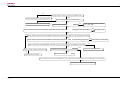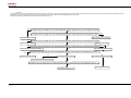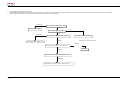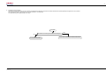
1
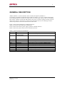
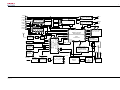
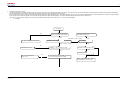
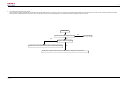
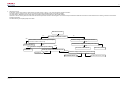
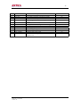
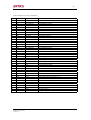
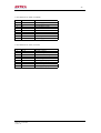
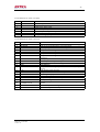
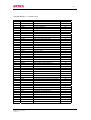
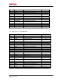
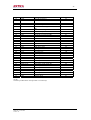
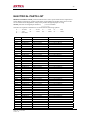
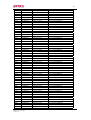
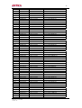
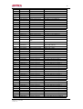
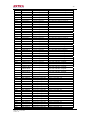
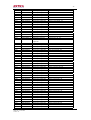
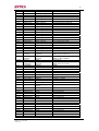
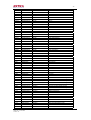
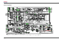
Colour TV
Service Manual
2
Model Group: CT-21FGS1
CHASSIS:
A21T01(TB1238)
MODEL:
CT-21FGS1
Model No: CT-21FGS1
Version 1.0
3
CONTENT
GERAL DESCRIPTION.......................................................................................................................... 4
SAFETY INSTRUCTION ....................................................................................................................... 6
CIRCUIT ADJUSTMENT....................................................................................................................... 7
FAULT FINDING TREES, DIAGRAMS & OVERVIEWS ................................................................. 14
VARIOUS PARAMETERS OF INTEGRATED CIRCUIT .................................................................. 22
ELECTRICAL PART LIST ................................................................................................................... 30
CIRCUIT DIAGRAM ............................................................................................................................ 40
Model No: CT-21FGS1
Version 1.0
4
GENERAL DESCRIPTION
AKIRA AKTP01 is a CTV monolithic chassis currently developed by AKIRA Co.
It introduces a monolithic IC TB1238AN developed by Toshiba Co. To carry out all the small signal
processing TB1238AN is a kind of IC used by color TV in PAL/NTSC system, which is controlled by
Inter IC Bus. Together with the SECAM decoder TA1275Z, it can form a signal processing circuit for
multi-system color TV. This chassis is used in many fashionable TV receiver technologies, which
makes the performance reach the advanced level of the world.
Figure 1 shows the block diagram of AKTP01(A21T01).
Table 1 provides A21T01 mainly ICs and functions.
Figure 2 shows the whole set power supply system for AKTP01(A21T01).
Figure 3 shows the system control circuit of AKTP01(A21T01).
Table 1: A21T01 mainly ICs and functions
Type
Location
Function Description
D901
87CM38N-3GN5/
System control microprocessor
87CK38N-2B46
D902
AT24C08
EEPROM
N101
N252
N203
N201
N402
N701
N202
N701
N711
A903
LA7910
CD4053BE
CD4053BE
TB1238AN
LA7830
TA1275AZ
CD4052BE
AN5270
AN5270
HS0038A
Model No: CT-21FGS1
Version 1.0
Band decoder
TV/AV switching
AV1/AV2 Switch
Small signal processor (IF/VIDEO/CHROMA/DEF)
Vertical output power amplifier
SECAM decoder
Sound system switching
Audio power amplifier (L)
Audio power amplifier(R)
Remote control receiver
5
L OUT
R OUT
V OUT
L IN1
R IN1
V IN1
L IN2
R IN2
V IN2
5
SIF TRAPS
Z235~Z238
TV/AV switching 4
N252 CD4053BE 15
14
2 1 9 1 1
13
1 2
SIF BPS
Z231~Z234
B
L
AUDIO AMPLIFIER
N711 AN5270 8
R
2
13
4
V23
VIDEO
OUT
V251
1 1 4switching
13 N203 CD4053BE
5
2 12 9 10 11
1 AV1/AV2
SAW
F
Z101
34
15
1
KEY
BOARD
REMOTE
RECEIVER
REMOTE
A903
35
VOL
A
VOL
B
6
5
1
SCL1
AC150-260V
50/60Hz
Resistance
disturbance
C501 L502
Bridge
rectification
VD503-VD506
3 3
1
3
22
§
25
VD
26
27
4
FIELD OUTPUT
POWER AMP.
N402(LA78040)
H
D
POWER SUPPLY
CIRCUIT
+300V
V512 V513 V511
Filte
T501 VD515
r
C507
7
19V
13V
24V
146
114
HORIZONTAL
DRIVE
V444
T401
5
HORIZONT
AL
OUTPUT
V411
HEAT
SDA1
1
14
35
47
43
IF VIDEO
EHT
FOCUS
SCREE
MEMORY
5
(D902)
ST24C08
6
15
13
Y
3
1
2
R-Y
SECAM DECODER
IF IN
3
3 N251 TA1275AZ
6
B-Y
IF IN
SMALL SIGNAL
3
5
7
SCP OUT
SDAO
PROCESSOR
3
1
SCLO 26(IF/VIDEO/CK\HROMA/DEF)29 SID OUT 21
27
R
AFC IN
N201
1
4
VIDEO
G
TB1238AN
H.SYN
1
AMPLIFIER
3
20 B V602,V612,V622
13~16 3
24
H OUT
V.OU
R,G,B, Y/BL
T
TV AUDIO
MICROCONTROLLOR
D901
87CM38N-3GN5
87CK38N-2B46
V10
1
V OUT
A
3
TUNER
TUN101
Model No: CT-21FGS1
Version 1.0
1
2
4
12 14 15
SOUND SYSTEM SWITCH
N202 CD4052BE
2 AUDIO AMPLIFIER8
N701 AN5270
4
FBT(T402)
BSC25
6
SAFETY INSTRUCTION
Warning: Before examining and servicing this chassis, read carefully the following safety
instruction.
X-RAY RADIATION PRECAUTION
1. The EHT must be checked every time the receiver is serviced to ensure that the CRT
does not emit X-ray radiation as result of excessive EHT voltage. The nominal EHT for
this receiver is 22KV at zero beam current (minimum brightness) operating at AC 220V.
The maximum EHT voltage permissible in any operating circumstances must not exceed
25KV. When checking the EHT, use the High Voltage Check procedure in this manual
using an accurate EHT voltmeter.
2. The only source of X-RAY radiation in this receiver is the CRT. To prevent X-ray
radiation, you should use the same type of CRT when replacing it.
3. Some components used in this receiver have safety-related characteristics preventing the
CRT from emitting X-ray radiation. For continued safety, replacement component should
only be made after referring the Product Safety notice below.
SAFETY PRECAUTION
1. The high voltage in the TV reaches to 22KV when the TV is in operation. Be more careful
during opening the back cover.
a. The high voltage existing in the TV is very dangerous. Refer servicing to qualified
personnel only.
b. Before removing the high voltage cap. Discharge the anode of the CRT and the
chassis in case of electric shock.
c. Wear a pair of goggles when handling the CRT to avoid broken pieces damaging
your eyes.
d. Do not hold the CRT neck in case of causing damage to the CRT.
2. When the power cord needs replacing, use the same one as that provided by AKIRA
factory.
3. Voltage exists between the hot and cold ground when TV is in operation. Install a
separation transformer during repairing or connecting to any tester for the sake of safety.
The power of the separation transformer should be beyond rated overall power.
4. When replacing a burnout fuse, use the one with the same specifications as the original.
5. When replacing old wire, wind new one round the shaft to weld. When replacing
components with safety in performance, use the same type as that specified by AKIRA
and install it in the former way.
6. Never place wire near high-temperature or high-voltage components.
SAFETY CAUTIONS FOR PRODUCTS
Many electric and mechanical components in AKPH01 /02 chassis have special safety
performances, which are always neglected. Even if replacing them with some components
with the same voltage and power, you can not get effective protection to X-ray. In the circuit
diagram, these special electric components are indicated by the special mark U! and on the
shadow. When replacing any of them, use the one with the same specifications as the
original’s. Otherwise, it may cause X-ray radiation and damage to overall safety.
Model No: CT-21FGS1
Version 1.0
7
CIRCUIT ADJUSTMENTS
GENERAL INFORMATIONS
All adjustment are thoroughly checked and corrected when the receiver leaves the factory.
Therefore the receiver should operate normally and produce proper color and B/W pictures
upon installation. However, several minor adjustments may be required depending on the
particular location in which the receiver is operated.
This receiver is shipped completely in carton. Carefully draw out the receiver from the carton
and remove all packing materials. Power cord into a convenient 220 volts 50 Hz AC two pin
power outlet. Turn the receiver ON. Check and adjust all the customer controls such as
BRIGHTNESS, CONTRAST and COLOUR Controls to obtain natural color or B/W picture.
AUTOMATIC DEGAUSSING
A degaussing coil is mounted around the picture tube so that external degaussing after
moving the receiver is normally unnecessary, providing the receiver is properly degaussed
upon installation. The degaussing coil operates for about 1 second after the power to the
receiver is switched ON. If the set is moved or faced in a different direction, the power switch
must be switched off at least 30 minutes in order that the automatic degaussing circuit
operates properly. Should the chassis or parts of the cabinet become magnetized to cause
poor color purity, use an external-degaussing coil. Slowly move the degaussing coil around
the faceplate of the picture tube, the side and front of the receiver and slowly withdraw the coil
to a distance of about 2m before disconnecting it from AC source. If color shading still
persists, perform the COLOUR PURITY ADJUSTMENT and CONVERGENCE
ADJUSTMENTS procedures.
ADJUSTMENT MODE
Item
B+ adjustment, TV signal receiving
AKPH01 chassis
Measuring
Equipment
No. 5 Service Remote Controller
Preparation
Before Adj.
The set is turned on and work normally.
No signal input
Model No: CT-21FGS1
Version 1.0
8
Adjustment procedure
1.
2.
Press S-PVOC key to set PIF-VOC self-adjusting.
OSD appears as below, after adjustment finished.
AFT
AFT OK
Self-adjusting
Adjusting OK
Note:
When the OSD appears ‘AFT NG’, it means that AFT adjusting is not good. Please check the chassis if
there is circuit short or parts wrong fitting. If not, counter-clockwise or clockwise turn a ferrite core in
T211 at 1/4 to 1/2 turn.
Item
B+ adjustment, TV signal receiving
AKTP01 chassis
Measuring
Equipment
TV SG (Signal Generator)
Digital multi-meter
Preparation
Before Adj.
The set is turned on
Connect the TV SG to RF input terminal of the set.
Adjustment procedure
1.
2.
Turn RP551 potentiometer to adjust B+ to specified voltage.
Check voltages for video out, vertical out, circuit work and audio power out as follow.
Voltage (volt)
Tolerance
14 inch
21 inch
Video Out
145
188
±5V
Vertical Out
26
26
±1V
Circuit Work
13
13
±1V
Audio Power Out
3.
19 for 3W
22 for 5W
19 for 3W
22 for 5W
±1V
TV signal receiving
a. Press MENU key, to select POS.MEMORY item.
b. Press V+ or V- key, to select SEARCH or AUTOMEMORY item, press P+ key to
start searching.
c. Press P+ or P- key to inspect the set if there is channel skipped, if so, searching again
by SEARCH as above described.
Model No: CT-21FGS1
Version 1.0
9
Item
TV system adapting & AV in/output inspection
AKTP01 chassis
Measuring
Equipment
SG (with NTSC3.58). User remote controller
Dual trace oscilloscope
Preparation
before Adj.
Input TV and AV signal
Inspection procedure
1.
2.
3.
4.
Input the TV signal which system is designated in technical specification.
Switch TV system to the set by pressing SYS key on user remote controller according to the TV
system in SG. The picture and sound must be normal.
Press TV/AV key, to select VIDEO1 or VIDEO2 input. The picture and sound must be normal
AV output inspection. Load a 75Ωresistor to VIDEO output terminal, 1Vp-p video output signal
that is from TV signal or from VIDEO1 or VIDEO2 input signal should be observed on the
oscilloscope. Load two 10K resistors separately to AUDIO R and L output terminals, two 0.7Vp-p
audio output signal that is from TV or from AV input signal (stereo) should be observed on the
oscilloscope.
Item
General adjustment
AKTP01 chassis
Measuring
Equipment
SG
No.1 and No.2 service remote controller and user remote controller
Preparation
before Adj.
Brightness, contrast and color should be set in standard
Press PP key repeatedly to set the picture at MEMORY2 (in standard)
Adjustment procedure
1.
2.
3.
4.
5.
6.
7.
Receive the monoscope pattern signal
Turn the focus adjusting VR to make the picture clear.
Press M-ON key on No.2 service remote controller to set the set into manufactory adjustment
mode.
Adjust the picture size roughly by No.2 service remote controller.
Grid 2 voltage adjustment. Press
key on No.1 service remote controller, to set the screen
into a horizontal line. Clockwise turn the screen VR gradually until a horizontal line appears on the
screen.
Press R+ or R- (with the red block), G+ or G- (with the green block) and B+ or B- (with the blue
block) key respectively, to adjust a horizontal line appeared to the white colour.
Press
key again and changing back to normal screen.
Model No: CT-21FGS1
Version 1.0
10
Item
Focus adjustment
AKTP01 chassis
Measuring
Equipment
SG
Preparation
before Adj.
Brightness, contrast and color should be set in standard
Adjustment procedure
1.
2.
Receive the cross-hatch pattern signal
Turn the focus adjusting VR watching the screen and adjust the vertical line of
mark to make
the most thin. Then the focus adj. VR is set as close low voltage side as possible.
Stop the focus adj. VR at the point that focus is a bit worse at once, turn back to the left and then
turn back to the right a little again.
To be fine
H. line
V. line
Magnified drawing of
Item
part
White balance adjustment
AKTP01 chassis
Measuring
Equipment
SG and white balance meter
No.1 service remote controller
Preparation
before Adj.
Warm up the set for more than 30 min.
Brightness, contrast and color should be set in standard
Adjustment procedure
1.
2.
3.
Receive the monoscope pattern signal.
Press G (G.DRIVE) key and B (B.DRIVE) key on No.1 service remote controller to select G-DRV
and B-DRV respectively, then press + or – key to adjust the white balance at the directed value
(which is according to the specification of factory’s adjustment)
Press R+ or R-, G+ or G- and B+ or B- key respectively to adjust the white balance of low light
until the white balance of high and low light is good
Model No: CT-21FGS1
Version 1.0
11
Item
RF. AGC adjustment
AKTP01 chassis
Measuring
Equipment
SG and digital multi meter
No.5 service remote controller
Preparation
before Adj.
Connect a digital multi meter to TP101 point on the chassis
Adjustment procedure
1.
2.
Receive the color bar signal that is 87.5% modulation and 60dBu level
Press RF AGC key on No.5 service remote controller to select RF. AGC adjustment, press + or –
key to adjust the voltage of RF AGC to 3.7±0.1V that is read on the digital multi meter.
Item
Vertical height, linearity and Hor. position adjustment
AKTP01 chassis
Measuring
Equipment
SG
No.2 and No.3 service remote controllers
Preparation
before Adj.
Brightness, contrast and color should be set in standard
Adjustment procedure
1.
2.
3.
4.
Receive the 5-circles pattern signal that is 50HZ vertical frequency.
Press V-LINE, V-SIZE, V-CENT and H-CENT key on NO.2 service remote controller
respectively to select the vertical linearity, height, center (position) and horizontal center (position)
adjustment, and then press + or - key to adjust the value of them respectively according to
factory’s specification.
Receive the 5-circles pattern signal that is 60HZ vertical frequency
Press V-LINE, V-SIZE, V-CENT and H-CENT key on NO.3 service remote controller separately
to adjust the vertical linearity, height, center and horizontal center as above item 3.
Item
OSD position adjustment
AKTP01 chassis
Measuring
Equipment
No.1 and No.5 service remote controller
Preparation
before Adj.
Brightness, contrast and color should be set in standard
Model No: CT-21FGS1
Version 1.0
12
Adjustment procedure
1.
Press D-MODE key on No.1 service remote controller to set the set into design mode adjustment.
2.
Press
or key to select OSD item, press
or
key to adjust the OSD to the center
position on the screen or press RF AGC key on No.5 service remote controller and press + or – key
to adjust the OSD position
Press D-MODE key again to quit design mode adjustment.
3.
Item
The functions of the set inspection
AKTP01 chassis
Measuring
Equipment
SG
User remote controller and No.
Preparation
Before Adj.
The set is turned on
Inspection procedure
1.
2.
3.
4.
5.
6.
7.
Receive the Philips pattern signal
Press PIC key on user remote controller to call the menu as adjusting picture quality. Adjust color,
brightness, contrast, sharpness and tint (in NTSC) respectively and all adjustment should be right
Press V+ key to increase the sound volume, no distortion heard at maximum level, press V- key to
decrease the sound volume, no sound heard at minimum level
Press POWER key to switch the set into standby status, at mean time the manufactory adjustment
mode is cancelled.
Press POWER key again, the set should work in normal receiving mode.
X (mute), DISP (display), PP and SLEEP key respectively, the relevant function should
Press
be normal
Press S-OUT key on No.5 service remote controller to set default value that stored in E2PROM on
the chassis for product shipment.
Model No: CT-21FGS1
Version 1.0
13
FAULT FINDING TREES, DIAGRAMS AND OVERVIEWS
1. Three-None (no raster, no picture, no sound)
This failure is mainly caused by big-power circuit such as power supply, horizontal scanning, vertical scanning.
The detail checking and repairing steps are as follow.
0V
50V
300V
Voltage of C507
NO
Test the voltage of C563
0V
Check if V501 collect-emitter
Was broken down
Check R502,F501,power
YES
Swich, AC cord and plug
Check the voltage
of V501 collector
115V
Cut off W560
NO
TTeesstt ootvariation
Norma
thheerr
vvoollttaaggee ssuucchh aass
118888VV,, 2244VV,, aanndd
LOW
V551,VD551,RP551,V552,
VD517,V572,V511
Check T501
N201 pin8 voltage
9V
Check VD556,C563
Check
R552,V551,VD551
VD515,V511,
V512,R555
N201 pin32 voltage
2V
V444 pin C voltage
0V
Check V501,V512,F501,R502,VD503
115V
Others
Check Z901,C901,
C902,N204
0V
24V
300V
Test voltage of V501 base
0.6V
Check
T501,VD517,
C515,C517,V411,
VD552-VD555
C415,C416,T402
C412
1V
115V Recover W560, unplug
XZ411 for a While,then
test the voltage of C563
0V
Others
No variation
Check if it get right
When cut off V572
Check V501
YES
Test the voltage of
D901 pin7
0V
4.5-5.5V
CPU has sent the
Check if V572
Power-off signal
is broken down
Model No: CT-21FGS1
Version 1.0
Check R320,V444
Check V411,T402,T401,
Deflection coil
Check L414,VD403,C411
Deflection coil
Check V411 pin C voltage
Check
VD553,C559,
]R437,C430,T401,
C415,V411
0V
115V
Check T402,V411,R449
Check T402
14
2. Two-None (no picture, no sound)
The failure shows that the set does not display the picture but it has noise wave or blue background or OSD on the screen. This means that the circuits of power supply, horizontal scanning, vertical scanning and video amplification
are normal and they are not considered in the repairing. The failures are mainly in the small signal processing circuits.
Before checking these circuits, a kind of practical test method is introduced. It is called “Signal-input way ”. The detail is described as follow: We can use the resistance function of an analog multimeter, connect the red pole (negative
in ohm scope) on the circuit board ground, then touch softly the test point with another pole (black pole) in ohm scope meanwhile observe the reactivity on the output device.
Note: In the TV test, we mainly observe the noise wave on the CRT and listen to the noise voice liking as “Ka…..Ka” from the loudspeakers.
a. No picture
No picture
NO
Check if A101 has input signal
YES
Check R553,N904,C973
Out of the “ 0-33V ” range
Check the “ VT ” voltage when auto searching
Check RF signal input and adaptor
In the “ 0-33V ” range
33V
The voltage on the C992
33V
0V
Check the “ +9V ” voltage on A101
CheckN902, TUN101
5V
Check the voltage on the C992
0-33V
Check R102, C102, TUN101
Check N101,R968,R969,
N201,A101
0V
The voltage between VL and BH vary from
0V to 9V or not when auto searching
Check ,V975,D901, R973, R975
,R975,R990,C971,C972,C991
Model No: CT-21FGS1
Version 1.0
15
2V
Check R119, R206, R101,C104,TUN101,N201
Exam the voltage of “ AGC ” on TUN101 without antenna
3.8V
0V
Test the voltage on pin 1, 3, 17,28,36of N201
9V
Check,V922, C203, C282,C263, VD261, C261
Test the voltage on pin 46 of N201
0V
Check N902, N201, C203,C282, R263,
C261,VD261,R261
5V
YES
Observe if there is snow-noise-wave disturbance on the CRT via using “Signal-input way ” by touching pin 6 and pin 8 of N201
Check N902, N201
NO
YES
Observe if there is snow-noise-wave disturbance on the CRT via using “ Signal-input way ” by touching pin 47 of N201
NO
YES
Observe if there is snow-noise-wave disturbance on the CRT via using “Signal-input way ”by touching pin 35 of N201
NO
Observe if snow-noise-wave disturbance on the CRT via using “ signal-input way ”by touching pin 39 of N201
NO
Check if voltage on pin 48 of N201 is 4.6V
2V
Check C212,TUN101,N201
Test if there is the sync signal on the pin 36 of N201
YES
Check V251,V212,V231,N201
YES
Check N251,N201,,R255,L251
NO
Check R321,VD436,T402,R462,C452
Observe if these is snow-noise-wave disturbance on the CRT via using “ Signal-input way ” by touching pin 18,19,20 of N201
NO
Check R273,R271,R272,V602,V612,V622,N201
Model No: CT-21FGS1
Version 1.0
16
b. No sound
In this kind of failure, first of all we should observe if there is the picture on the CRT. It proves the small signal circuit to work correctly with the picture on the CRT and we only check the sound signal processing and sound
amplification circuit. The repairing method (B1) may be referred without picture. The detail checking and repairing steps are as follow.
Note: Before repairing, assure that the volume is on and the state of set is in “TV”.
YES
Hear if there is the voice liking “Ka…Ka ” in the loudspeaker via using “ Signal-input way ” by touching pin 53 of N201
NO
Hear if there is the voice liking “Ka…Ka ” in the loudspeaker via using “ Signal-input way ” by touching pin 1 of N201
NO
Check R231, C214, N201
YES
Check N202,R231,C214,N201
YES Hear if there is the voice liking “Ka…Ka ” in the loudspeaker via using “ Signal-input way ” by touching pin4,15of N252
NO
Check C706,C716,N252
Check 9V-power supply
YES
YES
9V
Hear if there is the voice liking “Ka…Ka ” in the loudspeaker via using “ Signal-input way ” by touching pin 2,5 of N252
NO
Check N203,N201,V922,R210,R202
The voltage on pin 16 of N252
Hear if there is the voice liking “Ka…Ka ” in the loudspeaker via using “ Signal-input way ” by touching pin 2 of N701
YES
Check C706,C705, R203
5V
Check VD552,R910,C700,T501,N701
9V
NO
The voltage on pin 8 of N701
The voltage on pin 9,10,11of N252
24V
Hear if there is the voice liking “Ka…Ka ” in the loudspeaker via using “ Signal-input way ” by touching pin 2 of N711
9V
NO
Check SP301, SP302, N711
Model No: CT-21FGS1
Version 1.0
Check D901, N252,N203
17
3. Only horizontal line in the middle of the screen:
If vertical deflection circuit does not work, this kind of failure will happen. In deflection yoke, there only has horizontal sweeping, the electron beam in the CRT only moves in the horizontal orientation, so form this failure.
(While checking horizontal and vertical deflection circuit’ s failure, we have better to use an oscilloscope.)
Abnormal
Check C272,R279,N201
The waveform on the pin 24 of N201
Normal
The voltage on pin 3 of N402
Abnormal
0V
24V
Measuring the waveform on pin 4 of N402
Check R908, C448, N402, N201
Normal
Measuring the waveform on pin 2 of N402
Normal
Measuring the waveform on the deflection yoke
Abnormal
Check R442,C413,VD433,XZ411, deflection yoke
Model No: CT-21FGS1
Version 1.0
Check VD557, R550,V554,N402
The deflection yoke on the CRT
Abnormal
Check N402
18
4. Only vertical line in the middle of the screen
This is a dangerous failure. It probable causes flashover and smoking inside the set. Don’ t let your TV work for a long time as this failure appears. Because the electron beam can not move in the horizontal orientation, the failure
should be in the horizontal deflection circuit. We mainly check the open-circuit fault in horizontal deflection circuit. The detail checking and repairing steps are as follow:
Vertical line
The horizontal yoke is opened or not
YES
NO
YES
Whether “ XZ411” is opened
Check if there is bad solder between XZ411, and the main board
NO
Check L414, VD403, C412,C415,especial in inductive components and connector
Model No: CT-21FGS1
Version 1.0
Repair CRT
19
5. UOC does not work
In television, remote-control system is similar with the computer system. In theory , it can work if it holds two conditions as follow:
The power supply: In general, it is 5V, the error is not above 10% and the disturbance pulse is as small as possible.
The clock pulse: In TDA93XX circuit, the clock pulse is generated by pin58 / pin59 of N301 and 12M crystal oscillator.
Television’ s remote-control system also needs reset circuit that can preset the values in internal register. The circuit around pin57 of N204 is called auto-reset circuit. If UOC detects errors in resetting, it will come to the state of
programme protected.
The detail checking and repairing steps are as follow:
D901 does not work
5V
The voltage on the pin 42 of D901
5V
NO
Check the voltage on the positive pole of L901
=5V
Observe if there is sine wave on the pin 31 or pin
32 of D901 with an oscilloscope
Check Z900, D901
YES
4.98V
Check the voltage on the pin 33 of D901
Check D901
Check alternant voltage on secondary coil of T501,
Check the voltage on the emitter of V925
Check R937
4.98V
Check R939,VD922
Check T501, VD553,R558
4.98V
Check the voltage on the positive pole of VD921
4.98V
Check VD921, R933
Model No: CT-21FGS1
Version 1.0
NO
YES
4.98V
=3.6V
Check R932,R937,V925
20
6. No OSD (On Screen Display)
This failure is usually cause by the circuit of character generated and located. Most of reasons are that the horizontal and vertical flyback pulse signals do not come to UOC.
We can judge this failure by measuring the wave of the character in an oscilloscope.
The detail checking and repairing steps are as follow:
No OSD
Check the wave on the pin 4 of FBT and N402 pin7
YES
NO
Check FBT T402,N402
Model No: CT-21FGS1
Version 1.0
Check V922, V923,R914, VD436, R449, D901
21
VARIOUS PARAMETERS OF INTEGRATED CIRCUIT
A: Pin functions of N201( TB1238AN )
Pin
1
2
3
4
5
6
7
8
9
10
11
12
13
14
15
16
17
18
19
20
21
22
23
24
25
26
27
28
29
30
31
32
33
34
35
36
37
38
39
40
41
42
43
Symbol
DE-EMP
AUDIO OUT
IF VCC
AFT OUT
IF GND
IF IN
IF IN
RF AGC
IF AGC
APC FILTER
4.43MHZXTA
Y/C GND
YS/YM
EXT R IN
EXT G IN
EXT B IN
RGB VCC
R OUT
G OUT
B OUT
ABCL
V RAMP
V NFB
V OUT
V AGC
SCL
SDA
H VCC
SID/CW OUT
FBP IN
SYNC OUT
H OUT
DEF GND
FBP IN
VIDEO OUT
DIG. VD
S R-Y IN
S B-Y IN
Y IN
H AFC
EXT.VIDEO/Y IN
DIG.GND
TV.VIDEO IN
Model No: CT-21FGS1
Version 1.0
Function
Audio deemphasis capacitor connect pin
Audio signal output
+9V supply input for IF amplify circuit
AFT voltage output
Ground for IF amplifiter circuit
IF signal input
IF signal input
RF amplifier AGC control voltage output
IF amplifier AGC filter
APC filtering
4.43MHZ crystal oscillating
Ground (Y/C signal processor)
Y-switch signal input
Character R signal input
Character G signal input
Character B signal input
Supply input(RGB)
R output
G output
B output
Automatic brightness, contrast control
Vertical Ramp generator capacitor connect pin
V NFB input
Vertical pulse signal output
V AGC filter capacitor connect pin
(IIC)clock line
(IIC)data line
Horizontal deflection supply input (+9V)
SECAM identification/CW signal output
Horizontal flyback pulse input
SYNC pulse output
Horizontal excitation output
Ground (detection circuit)
Sandcastle pulse output
Video signal output
Digital circuit supply
SECAM R-Y signal input
SECAM B-Y signal input
Luminance signal input
Connecting RC network for horizontal AFC filter
External video/luminance signal input
Digital circuit ground
TV. video signal input
Dynamic state (v)
4.9
3.4
9
1.7
0
0
1.4
5.6
4.4
1.8
2.2
0
0
0.9
0.9
0.9
9
2.4
2.4
2.5
5.4
4.4
5
1
0.3
3.8
3.9
9.6
3.8
4.8
4.8
2
0
1.4
3
5.3
2.7
2.6
1.1
6.8
1.6
0
3.2
22
44
45
46
47
48
BLACK DEF
EXT.CIN
Y/C VCC
IF DETOUT
LOOP Filter
49
50
51
52
53
54
55
56
VCO GND
VCO
VCO
VCO VCC
Limiter IN
RIPPLE FILTER
EXT AUDIO
FM DEC NF
Model No: CT-21FGS1
Version 1.0
Black level detecting filter
External chroma signal input
+5V supply input (Y/C processing system)
IF video detected output
Connecting RC filter network for phase loop
circuit
Ground (IF VCO circuit)
Voltage control oscillating coil connecting pin
Voltage control oscillating coil connecting pin
+9V supply input (IF VCO circuit)
Sound IF signal input
Ripple filer circuit
External audio signal input
FM direct current negative feedback filter
capacitor can
2.4
2.9
5.2
3.7
4.8
0
8
8
9
3.8
4.8
3.4
3.8
23
B: Pin functions of N161 ( AN7522N )
Pin.
1
2
3
4
5
6
7
8
9
10
11
12
13
14
15
16
17
18
19
20
21
22
23
24
25
26
27
28
29
30
31
32
33
34
35
36
37
38
39
40
41
42
Pin name
VSS
P40
P41
P42
P43
P44
P45
P46
P47
P50
P51
P52
P53
P54
P55
P56
P60
P61
P62
P63
VSS
P64
P65
P66
P67
P70
P71
P72
P73
TEST
XIN
XOUT
RESET
P20
P30
P31
P34
P35
P57
P32
P33
VDD
Model No: CT-21FGS1
Version 1.0
Signal name
VSS
VT
EXT-MUTE
MUTE
VOLUME-L
VOLUME-R
POWER
Tone
BAND1
BAND2
SCL1
SDA1
AFC
AV2
KEY-IN1
KEY-IN2
AC POWER
SIF3
RF GAIN
50/60
VSS
R
G
B
Y
HD
VD
OSC1
OSC2
TEST
XIN
XOUT
RESET
AV1
REMOTE
H.SYNC
SCL0
SDA0
S-ID
SIF1
SIF2
VDD
Function
GND connection
VT output
External Mute Output
Mute Output
Left Volume PWM control
Right Volume PWM control
Power control &Check,On=Hi-Z(input),Off=L(outpot)
Tone control
BAND data output1
BAND data output2
IIC-BUS SCL1
IIC-BUS SDA1
AFC input
Video mode selection control No.2
Key input1
Key input2
AC POWER ON/OFF
SIF Output3
RF GAIN ON/OFF
50/60Hz Output
GND connection
OSD R signal output
OSD G signal output
OSD B signal output
OSD Y signal output
OSD HD signal output
OSD VD signal output
OSD oscillator connection
OSD oscillator connection
GND connection
8 MHz oscillator connection
8 MHz oscillator connection
Reset signal input
Video mode selection control No.1
Remote controller signal input
Horizontal sync signal input
IIC-BUS SCL0
IIC-BUS SDA0
S-VIDEO Detection
SIF data output1
SIF data output2
5V power supply
24
C: Pin functions of N402 ( LA78040 )
Pin
1
2
3
4
5
6
7
8
9
Symbol
Vcc1
IN
LF
VOL-CTL
TONE-CTL
RF
GND
OUT
Vcc2
Function
Power supply 1
Sound input
Low frequency input
Volume control
Tone control
Ripple filter
Ground
Sound output
Power supply 2
C: Pin functions of N101 ( LA7910)
Pin
1
2
3
4
5
6
7
8
9
Symbol
OUT1
OUT2
BD1
BD2
GND
VC2
OUT3
OUT4
VC1
Model No: CT-21FGS1
Version 1.0
Function
Decoder output 1
Decoder output 2
Band control level input 1
Band control level input 2
Connect to ground
+33V supply input pin
Decoder output 3
Decoder output 4
+12V supply input pin
25
D: Pin functions of N101 ( LA7830)
Pin
1
2
3
4
5
6
7
Symbol
GND
OUT
IN
Vcc
Function
Connect to ground
Field pulse output
Pump power supply input
V sawtooth pulse input
Connet to phase compensate capacitance
Power supply pin
Pump power supply output
D: Pin functions of N251 ( TA1275)
Pin
1
2
3
4
5
6
7
Symbol
YOUT
MODESW
R-Y OUT
R-Y BLACK CONTOL
B-Y OUT
B-Y BLACK CONTROL
S-ID FILTER
8
9
10
11
12
EXT. R-Y IN
5V Vcc
EXT.B-Y IN
GND
FO-ADJ. FILTER
13
14
15
16
17
18
C IN
BELLADJ. FILTER
Y IN
GND
SCP IN
5V Vc-c
19
4.43MHz CW IN
20
21
ID SW
SECAM ID IN/OUT
Model No: CT-21FGS1
Version 1.0
Function
The output pin for Y signal standard output level is 1.0Vp-p.
The pin for controlling the Y processing mode.
The output pin for demodulated R-Y signal
The pin for controlling the black offset level.
The output pin for demodulated B-Y signal.
The pin for controlling the black offset level.
The pin for connecting the SECAM identification filter
capactitor.
The input pin for external R-Y signal.
The Vcc pin for Y/C processing block.
The input pin for external B-Y signal.
The GND pin
The pin for connecting a capacitor for automatic adjusting
circuit
The chroma signal input pin.
The pin for connection the filter capacitor for the bell filter FO.
The Y signal input pin.
The pin for input the sandcastle pulse
Vc-c pin for logic block
The pin for input 4.43MHz of carrier wave for self-adjustment
circuit.
The switch pin for selecting the ID detection mode.
The interface pin to the main processor TB1238AN
26
The BUS DATA for 87CM38N-3GN5
Number
1.
2.
3.
4.
5.
6.
7.
8.
9.
10.
11.
12.
13.
14.
15.
16.
17.
18.
19.
20.
21.
22.
23.
24.
25.
26.
27.
28.
29.
30.
31.
32.
33.
34.
35.
36.
37.
38.
39.
40.
41.
42.
43.
44.
45.
46.
47.
Adjustment Item
RCUT
GCUT
BCUT
GDRV
BDRV
CNTX
BRTC
COLC
TNTC
COLP
COLS
SCNT
CNTC
CNTN
BRTX
BRTN
COLX
COLN
TNTX
TNTN
ST3
SV3
ST4
SV4
SHPX
SHPN
TXCX
RGCN
VM0
VM1
HPOS
Adjustment Function
Red Dard Balance
Green Dark Balance
Blue Dark Balance
Green light Balance
Blue light Balance
Sub Contrast Max
Sub-bright Centre
Sub Color Center(NTSC)
Sub Tint Center
Sub Color Center(PAL Difference)
Sub Color Center(SECAM)
Sub Contrast
Sub Contrast Center
Sub Contrast min
Sub-bright max(difference)
Sub-bright min(difference)
Sub color max(difference)
Sub color min
Sub tint max(difference)
Sub tint min(difference)
Sub sharp center(3.58NTSC TV)
Sub sharp center(3.58NTSC AV)
Sub sharp center(OTHER TV)
Sub sharp center(OTHER AV)
Sub sharpness max(difference)
Sub sharpness min(difference)
Text RGB contrast max
Text RGB contrast min
V/C/D mode data 0
V/C/D mode data 1
Horizontal center of 50 Hz
VP50
HIT
HPS
VP60
HITS
VLIN
VSC
VLIS
HIT0
HIT1
SBY
SRY
RAGC
AFT
HAFC
V25
Vertical centering of 50 Hz
Vertical amplitude of 50 Hz
Horizontal centering difference of 60 Hz
Vertical centering difference of 60 Hz
Vertical amplitude deflection of 60Hz
Vertical line of 50 Hz
Vertical S correction/50 Hz
Vertical line deflection of 60 Hz
50Hz SIZE ZOOM/WIDE V.
60Hz SIZE ZOOM/WIDE V.
SECAM B-Y Black
SECAM R-Y Black
RF AGC
PIF VCO center
AFC gain
Volume 25%
Model No: CT-21FGS1
Version 1.0
Type Data
5E
72
7D
3B
3E
3F
48
40
40
20
40
0B
30
00
30
30
35
00
28
28
25
25
25
25
35
35
35
25
0E
00
0A
06
2C
03
02
02
0B
07
00
19
00
08
08
25
40
00
37
27
48.
49.
50.
51.
52.
53.
54.
55.
56.
57.
58.
59.
60.
61.
62.
V50
BRTS
VM2
MOD0
MOD1
MOD2
SELF
SELF VOC
SELF AGC
SELF BRTC
SELF CNTC
SELF TNTC
SELF COL
OSD
OPT
Volume 50%
Sub bright ( difference )
TB1238AN V/C/D mode data
Factory data
Factory data
Factory data
TB1238AN P40UT select
Self adjust VCD initial data
Self adjust AGC initial data
Self adjust BRTC initial data
Self adjust CNTC initial data
Self adjust TNTCinitial data
Self adjust COL initial data
OSD position
Factory Data
5D
00
34
43
F5
0F
00
80
69
75
23
00
20
07
07
The BUS DATA for 87CK38N-2B46
Number
1.
2.
3.
4.
5.
6.
7.
8.
9.
10.
11.
12.
13.
14.
15.
16.
17.
18.
19.
20.
21.
22.
23.
24.
25.
26.
27.
28.
Adjustment Item
RCUT
GCUT
BCUT
GDRV
BDRV
CNTX
BRTC
COLC
TNTC
COLP
COLS
SCNT
CNTC
CNTN
BRTX
BRTN
COLX
COLN
TNTX
TNTN
ST3
SV3
ST4
SV4
SHPX
SHPN
TXCX
RGCN
Model No: CT-21FGS1
Version 1.0
Adjustment Function
Red Dard Balance
Green Dark Balance
Blue Dark Balance
Green light Balance
Blue light Balance
Sub Contrast Max
Sub-bright Centre
Sub Color Center(NTSC)
Sub Tint Center
Sub Color Center(PAL Difference)
Sub Color Center(SECAM)
Sub Contrast
Sub Contrast Center
Sub Contrast min
Sub-bright max(difference)
Sub-bright min(difference)
Sub color max(difference)
Sub color min
Sub tint max(difference)
Sub tint min(difference)
Sub sharp center(3.58NTSC TV)
Sub sharp center(3.58NTSC AV)
Sub sharp center(OTHER TV)
Sub sharp center(OTHER AV)
Sub sharpness max(difference)
Sub sharpness min(difference)
Text RGB contrast max
Text RGB contrast min
Type Data
5E
72
7D
3B
3E
3F
48
40
40
20
40
0B
30
00
30
30
35
00
28
28
25
25
25
25
35
35
35
25
28
29.
30.
31.
VM0
VM1
HPOS
V/C/D mode data 0
V/C/D mode data 1
Horizontal center of 50 Hz
0E
00
0A
32.
33.
34.
VP50
HIT
HPS
06
2C
03
35.
36.
37.
38.
39.
40.
41.
42.
43.
44.
45.
46.
47.
48.
49.
50.
51.
52.
53.
54.
55.
56.
57.
58.
59.
60.
61.
62.
VP60
HITS
VLIN
VSC
VLIS
HIT0
HIT1
SBY
SRY
RAGC
AFT
HAFC
V25
V50
BRTS
VM2
MOD0
MOD1
MOD2
SELF
SELF VOC
SELF AGC
SELF BRTC
SELF CNTC
SELF TNTC
SELF COL
OSD
OPT
Vertical centering of 50 Hz
Vertical amplitude of 50 Hz
Horizontal centering difference of 60
Hz
Vertical centering difference of 60 Hz
Vertical amplitude deflection of 60Hz
Vertical line of 50 Hz
Vertical S correction/50 Hz
Vertical line deflection of 60 Hz
50Hz SIZE ZOOM/WIDE V.
60Hz SIZE ZOOM/WIDE V.
SECAM B-Y Black
SECAM R-Y Black
RF AGC
PIF VCO center
AFC gain
Volume 25%
Volume 50%
Sub bright ( difference )
TB1238AN V/C/D mode data
Factory data
Factory data
Factory data
TB1238AN P40UT select
Self adjust VCD initial data
Self adjust AGC initial data
Self adjust BRTC initial data
Self adjust CNTC initial data
Self adjust TNTCinitial data
Self adjust COL initial data
OSD position
Factory Data
NOTE:
The data provided in the form provides to consult only!
Model No: CT-21FGS1
Version 1.0
02
02
0B
07
00
19
00
08
08
25
40
00
37
5D
00
34
43
70
05
00
80
69
75
23
00
20
07
07
29
ELECTRICAL PARTS LIST
PRODUCT SAFETY NOTE: products marked with a ! have special characteristics important to
safety. Before replacing any of these components, read carefully the product safety notice in this
service manual. Don’t degrade the safety of the product through improper servicing.
NOTE: parts that not assigned part numbers(
) are not available.
Tolerance of Capacitors and Resistors are noted with the following symbols.
C……….±0.25%
D……….±0.5%
F……….±1%
G………. ±2%
J………. ±5%
K………. ±10%
M…….. ±20%
N………. ±30%
Z………+80/-20%
Ref. No
R444
R632
R701
R711
R279
R602
R612
R622
R248
R219
R221
R266
R111
R201
R207
R210
R216
R218
R220
R222
R225
R226
R232
R238
R264
R265
R971
R972
R236
R404
R604
R614
R624
R106
R107
R217
R234
R241
R244
R247
Part No.
D10B4R7J-T
D10B4R7J-T
D10B4R7J-T
D10B4R7J-T
D10B330J-T
D10B330J-T
D10B330J-T
D10B330J-T
D10B680J-T
D10B750J-T
D10B750J-T
D10B750J-T
D10B101J-T
D10B101J-T
D10B101J-T
D10B101J-T
D10B101J-T
D10B101J-T
D10B101J-T
D10B101J-T
D10B101J-T
D10B101J-T
D10B101J-T
D10B101J-T
D10B101J-T
D10B101J-T
D10B101J-T
D10B101J-T
D10B151J-T
D10B151J-T
D10B151J-T
D10B151J-T
D10B151J-T
D10B221J-T
D10B221J-T
D10B221J-T
D10B221J-T
D10B221J-T
D10B221J-T
D10B221J-T
Model No: CT-21FGS1
Version 1.0
Name
Carbon resistor
Carbon resistor
Carbon resistor
Carbon resistor
Carbon resistor
Carbon resistor
Carbon resistor
Carbon resistor
Carbon resistor
Carbon resistor
Carbon resistor
Carbon resistor
Carbon resistor
Carbon resistor
Carbon resistor
Carbon resistor
Carbon resistor
Carbon resistor
Carbon resistor
Carbon resistor
Carbon resistor
Carbon resistor
Carbon resistor
Carbon resistor
Carbon resistor
Carbon resistor
Carbon resistor
Carbon resistor
Carbon resistor
Carbon resistor
Carbon resistor
Carbon resistor
Carbon resistor
Carbon resistor
Carbon resistor
Carbon resistor
Carbon resistor
Carbon resistor
Carbon resistor
Carbon resistor
Specification
RT13-1/6W-4.7Ω±5%
RT13-1/6W-4.7Ω±5%
RT13-1/6W-4.7Ω±5%
RT13-1/6W-4.7Ω±5%
RT13-1/6W-33Ω±5%
RT13-1/6W-33Ω±5%
RT13-1/6W-33Ω±5%
RT13-1/6W-33Ω±5%
RT13-1/6W-68Ω±5%
RT13-1/6W-75Ω±5%
RT13-1/6W-75Ω±5%
RT13-1/6W-75Ω±5%
RT13-1/6W-100Ω±5%
RT13-1/6W-100Ω±5%
RT13-1/6W-100Ω±5%
RT13-1/6W-100Ω±5%
RT13-1/6W-100Ω±5%
RT13-1/6W-100Ω±5%
RT13-1/6W-100Ω±5%
RT13-1/6W-100Ω±5%
RT13-1/6W-100Ω±5%
RT13-1/6W-100Ω±5%
RT13-1/6W-100Ω±5%
RT13-1/6W-100Ω±5%
RT13-1/6W-100Ω±5%
RT13-1/6W-100Ω±5%
RT13-1/6W-100Ω±5%
RT13-1/6W-100Ω±5%
RT13-1/6W-150Ω±5%
RT13-1/6W-150Ω±5%
RT13-1/6W-150Ω±5%
RT13-1/6W-150Ω±5%
RT13-1/6W-150Ω±5%
RT13-1/6W-220Ω±5%
RT13-1/6W-220Ω±5%
RT13-1/6W-220Ω±5%
RT13-1/6W-220Ω±5%
RT13-1/6W-220Ω±5%
RT13-1/6W-220Ω±5%
RT13-1/6W-220Ω±5%
30
R607
R617
R627
R633
R271
R272
R273
R203
R215
R205
R249
R250
R634
R937
R114
R115
R202
R233
R246
R251
R252
R267
R268
R269
R423
R517
R603
R613
R623
R635
R703
R705
R713
R719
R720
R907
R908
R934
R945
R948
R957
R958
R962
R973
R980
R985
R986
R987
R988
R640
R211
R274
R913
R932
W913
W914
R119
D10B221J-T
D10B221J-T
D10B221J-T
D10B221J-T
D10B271J-T
D10B271J-T
D10B271J-T
D10B471J-T
D10B471J-T
D10B561J-T
D10B561J-T
D10B561J-T
D10B561J-T
D10B561J-T
D10B102J-T
D10B102J-T
D10B102J-T
D10B102J-T
D10B102J-T
D10B102J-T
D10B102J-T
D10B102J-T
D10B102J-T
D10B102J-T
D10B102J-T
D10B102J-T
D10B102J-T
D10B102J-T
D10B102J-T
D10B102J-T
D10B102J-T
D10B102J-T
D10B102J-T
D10B102J-T
D10B102J-T
D10B102J-T
D10B102J-T
D10B102J-T
D10B102J-T
D10B102J-T
D10B102J-T
D10B102J-T
D10B102J-T
D10B102J-T
D10B102J-T
D10B102J-T
D10B102J-T
D10B102J-T
D10B102J-T
D10B122J-T
D10B152J-T
D10B152J-T
D10B152J-T
D10B152J-T
D10B152J-T
D10B152J-T
D10B222J-T
Model No: CT-21FGS1
Version 1.0
Carbon resistor
Carbon resistor
Carbon resistor
Carbon resistor
Carbon resistor
Carbon resistor
Carbon resistor
Carbon resistor
Carbon resistor
Carbon resistor
Carbon resistor
Carbon resistor
Carbon resistor
Carbon resistor
Carbon resistor
Carbon resistor
Carbon resistor
Carbon resistor
Carbon resistor
Carbon resistor
Carbon resistor
Carbon resistor
Carbon resistor
Carbon resistor
Carbon resistor
Carbon resistor
Carbon resistor
Carbon resistor
Carbon resistor
Carbon resistor
Carbon resistor
Carbon resistor
Carbon resistor
Carbon resistor
Carbon resistor
Carbon resistor
Carbon resistor
Carbon resistor
Carbon resistor
Carbon resistor
Carbon resistor
Carbon resistor
Carbon resistor
Carbon resistor
Carbon resistor
Carbon resistor
Carbon resistor
Carbon resistor
Carbon resistor
Carbon resistor
Carbon resistor
Carbon resistor
Carbon resistor
Carbon resistor
Carbon resistor
Carbon resistor
Carbon resistor
RT13-1/6W-220Ω±5%
RT13-1/6W-220Ω±5%
RT13-1/6W-220Ω±5%
RT13-1/6W-220Ω±5%
RT13-1/6W-270Ω±5%
RT13-1/6W-270Ω±5%
RT13-1/6W-270Ω±5%
RT13-1/6W-470Ω±5%
RT13-1/6W-470Ω±5%
RT13-1/6W-560Ω±5%
RT13-1/6W-560Ω±5%
RT13-1/6W-560Ω±5%
RT13-1/6W-560Ω±5%
RT13-1/6W-560Ω±5%
RT13-1/6W-1KΩ±5%
RT13-1/6W-1KΩ±5%
RT13-1/6W-1KΩ±5%
RT13-1/6W-1KΩ±5%
RT13-1/6W-1KΩ±5%
RT13-1/6W-1KΩ±5%
RT13-1/6W-1KΩ±5%
RT13-1/6W-1KΩ±5%
RT13-1/6W-1KΩ±5%
RT13-1/6W-1KΩ±5%
RT13-1/6W-1KΩ±5%
RT13-1/6W-1KΩ±5%
RT13-1/6W-1KΩ±5%
RT13-1/6W-1KΩ±5%
RT13-1/6W-1KΩ±5%
RT13-1/6W-1KΩ±5%
RT13-1/6W-1KΩ±5%
RT13-1/6W-1KΩ±5%
RT13-1/6W-1KΩ±5%
RT13-1/6W-1KΩ±5%
RT13-1/6W-1KΩ±5%
RT13-1/6W-1KΩ±5%
RT13-1/6W-1KΩ±5%
RT13-1/6W-1KΩ±5%
RT13-1/6W-1KΩ±5%
RT13-1/6W-1KΩ±5%
RT13-1/6W-1KΩ±5%
RT13-1/6W-1KΩ±5%
RT13-1/6W-1KΩ±5%
RT13-1/6W-1KΩ±5%
RT13-1/6W-1KΩ±5%
RT13-1/6W-1KΩ±5%
RT13-1/6W-1KΩ±5%
RT13-1/6W-1KΩ±5%
RT13-1/6W-1KΩ±5%
RT13-1/6W-1.2KΩ±5%
RT13-1/6W-1.5KΩ±5%
RT13-1/6W-1.5KΩ±5%
RT13-1/6W-1.5KΩ±5%
RT13-1/6W-1.5KΩ±5%
RT13-1/6W-1.5KΩ±5%
RT13-1/6W-1.5KΩ±5%
RT13-1/6W-2.2KΩ±5%
31
R204
R255
R949
R523
R925
R928
R996
R559
R108
R715
R922
R938
R118
R208
R263
R295
R511
R706
R716
R905
R921
R926
R940
R979
R253
R933
R110
R116
R117
R258
R291
R292
R293
R562
R906
R927
R935
R943
R951
R952
R955
R956
R959
R968
R969
R976
R977
R983
R984
R991
R992
R920
R993
R994
R102
R294
R929
D10B222J-T
D10B222J-T
D10B222J-T
D10B332J-T
D10B332J-T
D10B332J-T
D10B332J-T
D10B392J-T
D10B472J-T
D10B472J-T
D10B472J-T
D10B472J-T
D10B562J-T
D10B562J-T
D10B562J-T
D10B562J-T
D10B562J-T
D10B562J-T
D10B562J-T
D10B562J-T
D10B562J-T
D10B562J-T
D10B562J-T
D10B562J-T
D10B682J-T
D10B822J-T
D10B103J-T
D10B103J-T
D10B103J-T
D10B103J-T
D10B103J-T
D10B103J-T
D10B103J-T
D10B103J-T
D10B103J-T
D10B103J-T
D10B103J-T
D10B103J-T
D10B103J-T
D10B103J-T
D10B103J-T
D10B103J-T
D10B103J-T
D10B103J-T
D10B103J-T
D10B103J-T
D10B103J-T
D10B103J-T
D10B103J-T
D10B103J-T
D10B103J-T
D10B123J-T
D10B123J-T
D10B123J-T
D10B153J-T
D10B153J-T
D10B153J-T
Model No: CT-21FGS1
Version 1.0
Carbon resistor
Carbon resistor
Carbon resistor
Carbon resistor
Carbon resistor
Carbon resistor
Carbon resistor
Carbon resistor
Carbon resistor
Carbon resistor
Carbon resistor
Carbon resistor
Carbon resistor
Carbon resistor
Carbon resistor
Carbon resistor
Carbon resistor
Carbon resistor
Carbon resistor
Carbon resistor
Carbon resistor
Carbon resistor
Carbon resistor
Carbon resistor
Carbon resistor
Carbon resistor
Carbon resistor
Carbon resistor
Carbon resistor
Carbon resistor
Carbon resistor
Carbon resistor
Carbon resistor
Carbon resistor
Carbon resistor
Carbon resistor
Carbon resistor
Carbon resistor
Carbon resistor
Carbon resistor
Carbon resistor
Carbon resistor
Carbon resistor
Carbon resistor
Carbon resistor
Carbon resistor
Carbon resistor
Carbon resistor
Carbon resistor
Carbon resistor
Carbon resistor
Carbon resistor
Carbon resistor
Carbon resistor
Carbon resistor
Carbon resistor
Carbon resistor
RT13-1/6W-2.2KΩ±5%
RT13-1/6W-2.2KΩ±5%
RT13-1/6W-2.2KΩ±5%
RT13-1/6W-3.3KΩ±5%
RT13-1/6W-3.3KΩ±5%
RT13-1/6W-3.3KΩ±5%
RT13-1/6W-3.3KΩ±5%
RT13-1/6W-3.9KΩ±5%
RT13-1/6W-4.7KΩ±5%
RT13-1/6W-4.7KΩ±5%
RT13-1/6W-4.7KΩ±5%
RT13-1/6W-4.7KΩ±5%
RT13-1/6W-5.6KΩ±5%
RT13-1/6W-5.6KΩ±5%
RT13-1/6W-5.6KΩ±5%
RT13-1/6W-5.6KΩ±5%
RT13-1/6W-5.6KΩ±5%
RT13-1/6W-5.6KΩ±5%
RT13-1/6W-5.6KΩ±5%
RT13-1/6W-5.6KΩ±5%
RT13-1/6W-5.6KΩ±5%
RT13-1/6W-5.6KΩ±5%
RT13-1/6W-5.6KΩ±5%
RT13-1/6W-5.6KΩ±5%
RT13-1/6W-6.8KΩ±5%
RT13-1/6W-8.2KΩ±5%
RT13-1/6W-10KΩ±5%
RT13-1/6W-10KΩ±5%
RT13-1/6W-10KΩ±5%
RT13-1/6W-10KΩ±5%
RT13-1/6W-10KΩ±5%
RT13-1/6W-10KΩ±5%
RT13-1/6W-10KΩ±5%
RT13-1/6W-10KΩ±5%
RT13-1/6W-10KΩ±5%
RT13-1/6W-10KΩ±5%
RT13-1/6W-10KΩ±5%
RT13-1/6W-10KΩ±5%
RT13-1/6W-10KΩ±5%
RT13-1/6W-10KΩ±5%
RT13-1/6W-10KΩ±5%
RT13-1/6W-10KΩ±5%
RT13-1/6W-10KΩ±5%
RT13-1/6W-10KΩ±5%
RT13-1/6W-10KΩ±5%
RT13-1/6W-10KΩ±5%
RT13-1/6W-10KΩ±5%
RT13-1/6W-10KΩ±5%
RT13-1/6W-10KΩ±5%
RT13-1/6W-10KΩ±5%
RT13-1/6W-10KΩ±5%
RT13-1/6W-12KΩ±5%
RT13-1/6W-12KΩ±5%
RT13-1/6W-12KΩ±5%
RT13-1/6W-15KΩ±5%
RT13-1/6W-15KΩ±5%
RT13-1/6W-15KΩ±5%
32
R900
R970
R978
R1007
R1010
R515
R551
R571
R572
R904
R990
R278
R447
R914
R960
R965
R974
R975
R113
R206
R256
R448
R446
R923
R1006
R1009
R200
R254
R259
R989
R443
R101
R262
R455
R237
R257
R519
R261
R901
R944
R912
R526
R557
R424
R449
R522
R555
R556
R566
R554
R445
R442
R407
R560
R605
R615
R625
D10B183J-T
D10B183J-T
D10B183J-T
D10B223J-T
D10B223J-T
D10B223J-T
D10B223J-T
D10B223J-T
D10B223J-T
D10B223J-T
D10B223J-T
D10B333J-T
D10B333J-T
D10B333J-T
D10B333J-T
D10B333J-T
D10B333J-T
D10B333J-T
D10B473J-T
D10B473J-T
D10B473J-T
D10B473J-T
D10B563J-T
D10B563J-T
D10B683J-T
D10B683J-T
D10B104J-T
D10B104J-T
D10B104J-T
D10B104J-T
D10B124J-T
D10B224J-T
D10B224J-T
D10B224J-T
D10B824J-T
D10B225J-T
D10C220J-T
D10C221J-T
D10C471J-T
D10C681J-T
D10C102J-T
D10C272J-T
D10C472J-T
D10C153J-T
D10C153J-T
D10C153J-T
D10C473J-T
D10C473J-T
D10C104J-T
D10C154J-T
D10D1R8J-T
D10D331J-T
D10D102J-T
D10D332J-T
D10D332J-T
D10D332J-T
D10D332J-T
Model No: CT-21FGS1
Version 1.0
Carbon resistor
Carbon resistor
Carbon resistor
Carbon resistor
Carbon resistor
Carbon resistor
Carbon resistor
Carbon resistor
Carbon resistor
Carbon resistor
Carbon resistor
Carbon resistor
Carbon resistor
Carbon resistor
Carbon resistor
Carbon resistor
Carbon resistor
Carbon resistor
Carbon resistor
Carbon resistor
Carbon resistor
Carbon resistor
Carbon resistor
Carbon resistor
Carbon resistor
Carbon resistor
Carbon resistor
Carbon resistor
Carbon resistor
Carbon resistor
Carbon resistor
Carbon resistor
Carbon resistor
Carbon resistor
Carbon resistor
Carbon resistor
Carbon resistor
Carbon resistor
Carbon resistor
Carbon resistor
Carbon resistor
Carbon resistor
Carbon resistor
Carbon resistor
Carbon resistor
Carbon resistor
Carbon resistor
Carbon resistor
Carbon resistor
Carbon resistor
Carbon resistor
Carbon resistor
Carbon resistor
Carbon resistor
Carbon resistor
Carbon resistor
Carbon resistor
RT13-1/6W-18KΩ±5%
RT13-1/6W-18KΩ±5%
RT13-1/6W-18KΩ±5%
RT13-1/6W-22KΩ±5%
RT13-1/6W-22KΩ±5%
RT13-1/6W-22KΩ±5%
RT13-1/6W-22KΩ±5%
RT13-1/6W-22KΩ±5%
RT13-1/6W-22KΩ±5%
RT13-1/6W-22KΩ±5%
RT13-1/6W-22KΩ±5%
RT13-1/6W-33KΩ±5%
RT13-1/6W-33KΩ±5%
RT13-1/6W-33KΩ±5%
RT13-1/6W-33KΩ±5%
RT13-1/6W-33KΩ±5%
RT13-1/6W-33KΩ±5%
RT13-1/6W-33KΩ±5%
RT13-1/6W-47KΩ±5%
RT13-1/6W-47KΩ±5%
RT13-1/6W-47KΩ±5%
RT13-1/6W-47KΩ±5%
RT13-1/6W-56KΩ±5%
RT13-1/6W-56KΩ±5%
RT13-1/6W-68KΩ±5%
RT13-1/6W-68KΩ±5%
RT13-1/6W-100KΩ±5%
RT13-1/6W-100KΩ±5%
RT13-1/6W-100KΩ±5%
RT13-1/6W-100KΩ±5%
RT13-1/6W-120KΩ±5%
RT13-1/6W-220KΩ±5%
RT13-1/6W-220KΩ±5%
RT13-1/6W-220KΩ±5%
RT13-1/6W-820KΩ±5%
RT13-1/6W-2.2MΩ±5%
RT14-1/4W-22Ω±5%
RT14-1/4W-220Ω±5%
RT14-1/4W-470Ω±5%
RT14-1/4W-680Ω±5%
RT14-1/4W-1KΩ±5%
RT14-1/4W-2.7KΩ±5%
RT14-1/4W-4.7KΩ±5%
RT14-1/4W-15KΩ±5%
RT14-1/4W-15KΩ±5%
RT14-1/4W-15KΩ±5%
RT14-1/4W-47KΩ±5%
RT14-1/4W-47KΩ±5%
RT14-1/4W-100KΩ±5%
RT14-1/4W-150KΩ±5%
RT15-1/2W-1.8Ω±5%
RT15-1/2W-330Ω±5%
RT15-1/2W-1KΩ±5%
RT15-1/2W-3.3KΩ±5%
RT15-1/2W-3.3KΩ±5%
RT15-1/2W-3.3KΩ±5%
RT15-1/2W-3.3KΩ±5%
33
R462
R552
R520
R521
R501
R561
R413
R630
R564
R606
R616
R626
R525
R936
R939
R437
R553
R563
R524
R531 !
D10D682J-T
D10D473J-T
D10D104J-T
D10D104J-T
D10D224J-T
D10D224J-T
S10E102J-S(A)
S10F3R3J-C
S10E471J-C
S10F123J-C
S10F123J-C
S10F123J-C
S10F680J-C
S10F680J-C
S10F121J-C
S10F271J-C
S10F123J-C
S10F123J-C
S10G390J-C
R558 !
R550 !
F10DR47J-C
R910!
W560
R502 !
PS551
RP501
C270
C925
C926
C115
C283
C116
C214
C232
C233
C234
C236
C257
C290
C213
C602
C612
C622
C927
C928
C971
C972
C974
C601
C611
C621
C448
C446
C919
F10D1R0J-C
F10D1R0J-C
W11H3R9K
W10J3R9K
P10X180J-C
V11D202B
C2CF150J-T
C2CF150J-T
C2CF150J-T
C2CF180J-T
C2CF470J-T
C2CF680J-T
C2BF101K-T
C2BF101K-T
C2BF101K-T
C2BF101K-T
C2BF101K-T
C2BF101K-T
C2BF101K-T
C2BF221K-T
C2BF221K-T
C2BF221K-T
C2BF221K-T
C2BF221K-T
C2BF221K-T
C2BF221K-T
C2BF221K-T
C2BF221K-T
C2BF561K-T
C2BF561K-T
C2BF561K-T
C2BF681K-T
C2BF102K-T
C2BF102K-T
Model No: CT-21FGS1
Version 1.0
Carbon resistor
Carbon resistor
Carbon resistor
Carbon resistor
Carbon resistor
Carbon resistor
Metal oxide resistor
Metal oxide resistor
Metal oxide resistor
Metal oxide resistor
Metal oxide resistor
Metal oxide resistor
Metal oxide resistor
Metal oxide resistor
Metal oxide resistor
Metal oxide resistor
Metal oxide resistor
Metal oxide resistor
Metal oxide resistor
Glass-Glazed Fixed
RES
Fuse resistor
Fuse resistor
Fuse resistor
Wire-wound resistor
Wire-wound resistor
Thermistor
Potentiometer
Ceramic capacitor
Ceramic capacitor
Ceramic capacitor
Ceramic capacitor
Ceramic capacitor
Ceramic capacitor
Ceramic capacitor
Ceramic capacitor
Ceramic capacitor
Ceramic capacitor
Ceramic capacitor
Ceramic capacitor
Ceramic capacitor
Ceramic capacitor
Ceramic capacitor
Ceramic capacitor
Ceramic capacitor
Ceramic capacitor
Ceramic capacitor
Ceramic capacitor
Ceramic capacitor
Ceramic capacitor
Ceramic capacitor
Ceramic capacitor
Ceramic capacitor
Ceramic capacitor
Ceramic capacitor
Ceramic capacitor
RT15-1/2W-6.8KΩ±5%
RT15-1/2W-47KΩ±5%
RT15-1/2W-100KΩ±5%
RT15-1/2W-100KΩ±5%
RT15-1/2W-220KΩ±5%
RT15-1/2W-220KΩ±5%
RY16/RY21-1W-1KΩ±5%
RY17/RY21-2W-3.3Ω±5%
RY16/RY21-1W-470Ω±5%
RY16/RY21-2W-12KΩ±5%
RY16/RY21-2W-12KΩ±5%
RY16/RY21-2W-12KΩ±5%
RY17/RY21-2W-68Ω±5%
RY17/RY21-2W-68Ω±5%
RY17/RY21-2W-120Ω±5%
RY17/RY21-2W-270Ω±5%
RY17/RY21-2W-12KΩ±5%
RY17/RY21-2W-12KΩ±5%
RY18/RY21-3W-39Ω±5%
RI40-1/2W-24MΩ±5%
RF10-1/2W-0.47Ω±5%
RF10-1/2W-1Ω±5%
RF10-1/2W-1Ω±5%
RXG6-5W-3.9Ω-J
RXG6-6W-3.9Ω-J
PTC-180HM
WI06-2AA2KΩ
CC1-06A-CH-50/63V-15pF-J
CC1-06A-CH-50/63V-15pF-J
CC1-06A-CH-50/63V-15pF-J
CC1-06A-CH-50/63V-18pF-J
CC1-06A-CH-50/63V-47pF-J
CC1-06A-CH-50/63V-68pF-J
CC1-06A-RH-50/63V-100pF-J
CC1-06A-RH-50/63V-100pF-J
CC1-06A-RH-50/63V-100pF-J
CC1-06A-RH-50/63V-100pF-J
CC1-06A-RH-50/63V-100pF-J
CC1-06A-RH-50/63V-100pF-J
CC1-06A-RH-50/63V-100pF-J
CC1-06A-RH-50/63V-220pF-J
CC1-06A-RH-50/63V-220pF-J
CC1-06A-RH-50/63V-220pF-J
CC1-06A-RH-50/63V-220pF-J
CC1-06A-RH-50/63V-220pF-J
CC1-06A-RH-50/63V-220pF-J
CC1-06A-RH-50/63V-220pF-J
CC1-06A-RH-50/63V-220pF-J
CC1-06A-RH-50/63V-220pF-J
CC1-06A-RH-50/63V-560pF-J
CC1-06A-RH-50/63V-560pF-J
CC1-06A-RH-50/63V-560pF-J
CC1-06A-RH-50/63V-680pF-J
CT1-06A-2B4-50/63V-1000pF-K
CT1-06A-2B4-50/63V-1000pF-K
34
C934
C269
C447
C112
C113
C217
C221
C225
C226
C258
C266
C250
C251
C281
C299
C704
C714
C924
C929
C933
C921
C402
C450
C403
C452
C503
C504
C505
C506
C553
C554
C555
C560
C418
C516
C630
C535 !
C209
C210
C216
C224
C228
C634
C707
C717
C936
C108
C218
C239
C240
C241
C242
C558
C706
C716
C203
C2BF102K-T
C2BF182K-T
C2BF182K-T
C2FF103Z-T
C2FF103Z-T
C2FF103Z-T
C2FF103Z-T
C2FF103Z-T
C2FF103Z-T
C2FF103Z-T
C2FF103Z-T
C2FF103Z-T
C2FF103Z-T
C2FF103Z-T
C2FF103Z-T
C2FF103Z-T
C2FF103Z-T
C2FF103Z-T
C2FF103Z-T
C2FF103Z-T
C2RF121J-T
C2BP102K-T
C2BP102K-T
C2BP392K-T
C2BP392K-T
C2BW102K-O
C2BW102K-O
C2BW102K-O
C2BW102K-O
C2BW471K-O
C2BW471K-O
C2BW471K-O
C2BW471K-O
C2RX471K-O
C2RX681K-O
C2EX222Z-O
C2EM102M-O
E20C100M-T
E20C100M-T
E20C100M-T
E20C100M-T
E20C100M-T
E20C100M-T
E20C100M-T
E20C100M-T
E20C100M-T
E20C220M-T
E20C220M-T
E20C220M-T
E20C220M-T
E20C220M-T
E20C220M-T
E20C220M-T
E20C220M-T
E20C220M-T
E20C470M-T
Model No: CT-21FGS1
Version 1.0
Ceramic capacitor
Ceramic capacitor
Ceramic capacitor
Ceramic capacitor
Ceramic capacitor
Ceramic capacitor
Ceramic capacitor
Ceramic capacitor
Ceramic capacitor
Ceramic capacitor
Ceramic capacitor
Ceramic capacitor
Ceramic capacitor
Ceramic capacitor
Ceramic capacitor
Ceramic capacitor
Ceramic capacitor
Ceramic capacitor
Ceramic capacitor
Ceramic capacitor
Ceramic capacitor
Ceramic capacitor
Ceramic capacitor
Ceramic capacitor
Ceramic capacitor
Ceramic capacitor
Ceramic capacitor
Ceramic capacitor
Ceramic capacitor
Ceramic capacitor
Ceramic capacitor
Ceramic capacitor
Ceramic capacitor
Ceramic capacitor
Ceramic capacitor
Ceramic capacitor
Ceramic capacitor
Electrolytic Capacitor
Electrolytic Capacitor
Electrolytic Capacitor
Electrolytic Capacitor
Electrolytic Capacitor
Electrolytic Capacitor
Electrolytic Capacitor
Electrolytic Capacitor
Electrolytic Capacitor
Electrolytic Capacitor
Electrolytic Capacitor
Electrolytic Capacitor
Electrolytic Capacitor
Electrolytic Capacitor
Electrolytic Capacitor
Electrolytic Capacitor
Electrolytic Capacitor
Electrolytic Capacitor
Electrolytic Capacitor
CT1-06A-2B4-50/63V-1000pF-K
CT1-06A-2B4-50/63V-1800pF-K
CT1-06A-2B4-50/63V-1800pF-K
CT1-08A-2F4-50/63V-0.01uF-Z
CT1-08A-2F4-50/63V-0.01uF-Z
CT1-08A-2F4-50/63V-0.01uF-Z
CT1-08A-2F4-50/63V-0.01uF-Z
CT1-08A-2F4-50/63V-0.01uF-Z
CT1-08A-2F4-50/63V-0.01uF-Z
CT1-08A-2F4-50/63V-0.01uF-Z
CT1-08A-2F4-50/63V-0.01uF-Z
CT1-08A-2F4-50/63V-0.01uF-Z
CT1-08A-2F4-50/63V-0.01uF-Z
CT1-08A-2F4-50/63V-0.01uF-Z
CT1-08A-2F4-50/63V-0.01uF-Z
CT1-08A-2F4-50/63V-0.01uF-Z
CT1-08A-2F4-50/63V-0.01uF-Z
CT1-08A-2F4-50/63V-0.01uF-Z
CT1-08A-2F4-50/63V-0.01uF-Z
CT1-08A-2F4-50/63V-0.01uF-Z
CC1-06A-RH-50/63V-120pF-Z
CT1-08C-2B4-500V-1000pF-K
CT1-08C-2B4-500V-1000pF-K
CT1-08C-2B4-500V-3900pF-K
CT1-08C-2B4-500V-3900pF-K
CT81-08C-2R-1KV-1000pF-K
CT81-08C-2R-1KV-1000pF-K
CT81-08C-2R-1KV-1000pF-K
CT81-08C-2R-1KV-1000pF-K
CT81-08C-2R-1KV-470pF-K
CT81-08C-2R-1KV-470pF-K
CT81-08C-2R-1KV-470pF-K
CT81-08C-2R-1KV-470pF-K
CT81-08C-2R-2KV-470pF-K
CT81-08C-2R-2KV-680pF-K
CT81-08C-2R-2KV-2200pF-K
CTJ1-AC250V-1000PF-±20%
CD110-16V-10uF –M
CD110-16V-10uF –M
CD110-16V-10uF –M
CD110-16V-10uF –M
CD110-16V-10uF –M
CD110-16V-10uF –M
CD110-16V-10uF –M
CD110-16V-10uF –M
CD110-16V-10uF -M
CD110-16V-22uF -M
CD110-16V-22uF -M
CD110-16V-22uF -M
CD110-16V-22uF -M
CD110-16V-22uF -M
CD110-16V-22uF -M
CD110-16V-22uF -M
CD110-16V-22uF -M
CD110-16V-22uF -M
CD110-16V-47uF –M
35
C259
C292
C632
C904
C996
C103
C235
C261
C236
C282
C993
C230
C703
C932
C935
C272
C279
C421
C557
C702
C712
C433
C430
C435
C449
C559
C552
C565
C700
C212
C277
C117
C231
C271
C223
C249
C256
C265
C291
C109
C973
C975
C977
C978
C101
C104
C105
C107
C208
C220
C227
C229
C443
C976
C411
C563
E20C470M-T
E20C470M-T
E20C470M-T
E20C470M-T
E20C470M-T
E20C101M-T
E20C101M-T
E20C101M-T
E20C101M-T
E20C101M-T
E20C101M-T
E20C101M-T
E20C101M-T
E20C101M-T
E20C101M-T
E20D1R0KT-T
E20D1R0KT-T
E20D4R7MNT
E20D471M
E20D471M
E20D471M
E20D102M
E20E470M-T
E20E470M-T
E20E101M-T
E20E331M
E20E102M
E20E102M
E20E102M
E20FR22M-T
E20FR22M-T
E20FR47M-T
E20FR47M-T
E20FR47M-T
E20F1R0M-T
E20F1R0M-T
E20F1R0M-T
E20F1R0M-T
E20F1R0M-T
E20F2R2M-T
E20F2R2M-T
E20F2R2M-T
E20F2R2M-T
E20F2R2M-T
E20F4R7M-T
E20F4R7M-T
E20F4R7M-T
E20F4R7M-T
E20F4R7M-T
E20F4R7M-T
E20F4R7M-T
E20F4R7M-T
E20F4R7M-T
E20F4R7M-T
E21H1R0M-T
E20H101M
Model No: CT-21FGS1
Version 1.0
Electrolytic Capacitor
Electrolytic Capacitor
Electrolytic Capacitor
Electrolytic Capacitor
Electrolytic Capacitor
Electrolytic Capacitor
Electrolytic Capacitor
Electrolytic Capacitor
Electrolytic Capacitor
Electrolytic Capacitor
Electrolytic Capacitor
Electrolytic Capacitor
Electrolytic Capacitor
Electrolytic Capacitor
Electrolytic Capacitor
Tantalum Capacitor
Tantalum Capacitor
NON-POLAR
Capacitor
Electrolytic Capacitor
Electrolytic Capacitor
Electrolytic Capacitor
Electrolytic Capacitor
Electrolytic Capacitor
Electrolytic Capacitor
Electrolytic Capacitor
Electrolytic Capacitor
Electrolytic Capacitor
Electrolytic Capacitor
Electrolytic Capacitor
Electrolytic Capacitor
Electrolytic Capacitor
Electrolytic Capacitor
Electrolytic Capacitor
Electrolytic Capacitor
Electrolytic Capacitor
Electrolytic Capacitor
Electrolytic Capacitor
Electrolytic Capacitor
Electrolytic Capacitor
Electrolytic Capacitor
Electrolytic Capacitor
Electrolytic Capacitor
Electrolytic Capacitor
Electrolytic Capacitor
Electrolytic Capacitor
Electrolytic Capacitor
Electrolytic Capacitor
Electrolytic Capacitor
Electrolytic Capacitor
Electrolytic Capacitor
Electrolytic Capacitor
Electrolytic Capacitor
Electrolytic Capacitor
Electrolytic Capacitor
Electrolytic Capacitor
Electrolytic Capacitor
CD110-16V-47uF –M
CD110-16V-47uF –M
CD110-16V-47uF –M
CD110-16V-47uF –M
CD110-16V-47uF –M
CD110-16V-100uF –M
CD110-16V-100uF –M
CD110-16V-100uF –M
CD110-16V-100uF –M
CD110-16V-100uF –M
CD110-16V-100uF –M
CD110-16V-470uF –M
CD110-16V-470uF –M
CD110-16V-470uF –M
CD110-16V-470uF –M
CA42-25V-1 uF –M
CA42-25V-1 uF –M
CD71-BP-25V-4.7uF-M
CD110-25V-470uF –M
CD110-25V-470uF –M
CD110-25V-470uF –M
CD110-25V-1000uF -M
CD110-35V-47uF -M
CD110-35V-47uF -M
CD110-35V-100uF -M
CD110-35V-330uF -M
CD110-35V-1000uF -M
CD110-35V-1000uF -M
CD110-35V-1000uF -M
CD110-50V-0.22uF -M
CD110-50V-0.22uF -M
CD110-50V-0.47uF –M
CD110-50V-0.47uF –M
CD110-50V-0.47uF –M
CD110-50V-1uF –M
CD110-50V-1uF –M
CD110-50V-1uF –M
CD110-50V-1uF –M
CD110-50V-1uF –M
CD110-50V-2.2uF –M
CD110-50V-2.2uF –M
CD110-50V-2.2uF –M
CD110-50V-2.2uF -M
CD110-50V-2.2uF -M
CD110-50V-4.7uF –M
CD110-50V-4.7uF –M
CD110-50V-4.7uF –M
CD110-50V-4.7uF -M
CD110-50V-4.7uF –M
CD110-50V-4.7uF –M
CD110-50V-4.7uF –M
CD110-50V-4.7uF -M
CD110-50V-4.7uF –M
CD110-50V-4.7uF -M
CD110-160V-1uF -M
CD110-160V-100uF-M
36
C562
C507
C278
C202
C705
C715
C515
C264
C517
C260
C102
C238
C253
C254
C255
C701
C711
C991
C992
C413
C444
C514
C412
E20K221M
E20M121M
F20F222J-T
F20F472J-T
F20F472J-T
F20F472J-T
F22F123J-T
F20F223K-T
F20F223K-T
F20F333K-T
F20F104K-T
F20F104K-T
F20F104K-T
F20F104K-T
F20F104K-T
F20F104K-T
F20F104K-T
F20F104K-T
F20F104K-T
F20G104K-T
F20G104K-T
F20G104K-T
F20J394J
C415 !
Ref. No
C501 !
F20Z822J
Part No.
L414
T102
T211
L232
L233
L231
L251
L252
L253
L501 !
VD515 !
F20R224M
LXXX0040
TLXX0004
TLXX0017
L3X14R7K-T
L3X14R7K-T
L3X18R2K-T
L3X1150K-T
L3X1150K-T
L3X1150K-T
LMXX0002
RX0001XX
VD1001
VD266
VD514
VD516
VD518
VD558
VD559
VD601
VD611
VD621
VD630
VD631
VD904
VD910
VD911
VD961
DL0008XX
DR0001XX-T
DR0001XX-T
DR0001XX-T
DR0001XX-T
DR0001XX-T
DR0001XX-T
DR0001XX-T
DR0001XX-T
DR0001XX-T
DR0001XX-T
DR0001XX-T
DR0001XX-T
DR0001XX-T
DR0001XX-T
DR0001XX-T
Model No: CT-21FGS1
Version 1.0
Electrolytic Capacitor
Electrolytic Capacitor
Mylar capacitor
Mylar capacitor
Mylar capacitor
Mylar capacitor
Mylar capacitor
Mylar capacitor
Mylar capacitor
Mylar capacitor
Mylar capacitor
Mylar capacitor
Mylar capacitor
Mylar capacitor
Mylar capacitor
Mylar capacitor
Mylar capacitor
Mylar capacitor
Mylar capacitor
Mylar capacitor
Mylar capacitor
Mylar capacitor
Polypropylene
capacitor
Polypropylene
capacitor
Name
Polypropylene
capacitor
H-linear
Coil
Coil
Inductor
Inductor
Inductor
Inductor
Inductor
Inductor
Degaussing coil
Photoelectricity
coupler
LED
Diode
Diode
Diode
Diode
Diode
Diode
Diode
Diode
Diode
Diode
Diode
Diode
Diode
Diode
Diode
CD288-250V-22uF -M
CD293-400V-120uF-±10%
CL11-50V/63V-2200PF-K
CL11-50V/63V-4700PF-K
CL11-50V/63V-4700PF-K
CL11-50V/63V-4700PF-K
CL21X-50V/63V-0.012uF-K
CL11-50V/63V-0.022uF-K
CL11-50V/63V-0.022uF-K
CL11-50V/63V-0.033uF-K
CL11-50V/63V-0.1uF-K
CL11-50V/63V-0.1uF-K
CL11-50V/63V-0.1uF-K
CL11-50V/63V-0.1uF-K
CL11-50V/63V-0.1uF-K
CL11-50V/63V-0.1uF-K
CL11-50V/63V-0.1uF-K
CL11-50V/63V-0.1uF-K
CL11-50V/63V-0.1uF-K
CL11-100V-0.1uF-K
CL11-100V-0.1uF-K
CL11-100V-0.1uF-K
CBB21-200V-0.39uF±5%
CBB81-1.6KV-8200PF-J
Specification
CBB62-250VAC-0.22uF
LX40
04b
IF DETECTOR TANK
LGA0307-4.7uH-K
LGA0307-4.7uH-K
LGA0307-8.2uH-K
LGA0307-15uH-K
LGA0307-15uH-K
LGA0307-15uH-K
PC817B/C
RED 5mm
IS1555/IN4148A
IS1555/IN4148A
IS1555/IN4148A
IS1555/IN4148A
IS1555/IN4148A
IS1555/IN4148A
IS1555/IN4148A
IS1555/IN4148A
IS1555/IN4148A
IS1555/IN4148A
IS1555/IN4148A
IS1555/IN4148A
IS1555/IN4148A
IS1555/IN4148A
IS1555/IN4148A
37
VD968
VD970
VD972
VD973
VD517
VD552
VD553
VD557
VD434
VD503
VD504
VD505
VD506
VD556
VD554
VD555
VD551
VD703
Ref. No
VD713
VD436
VD261
VD922
VD921
VD901
VD519
N101
N251
N202
N904
N201
D901
N203
N701
N711
N252
N902
N402
D901
V213
V231
V251
V511
V631
V925
V994
V921
V552
V101
V602
V612
V622
V444
V512
V513
V102
V201
DR0001XX-T
DR0001XX-T
DR0001XX-T
DR0001XX-T
DR0003XX-T
DR0003XX-T
DR0003XX-T
DR0003XX-T
DR0009XX-T
DR0015XX-T
DR0015XX-T
DR0015XX-T
DR0015XX-T
DR0017XX
DR0018XX
DR0031XX-T
DZ0001XX-T
DZ0001XX-T
Part No.
DZ0001XX-T
DZ0002XX-T
DZ0002XX-T
DZ0002XX-T
DZ0006XX-T
DZ0015XX-T
DZ0010XX-T
IXXX0020
IXXX0024
IXXX0026
IXXX0080
IXXX0023
IXXX0106
IXXX0120
IXXX0033
IXXX0033
IXXX0120
IXXX0118
IXXX0043
IXXX0079
RXA1015X-T
RXA1015X-T
RXA1015X-T
RXA1015X-T
RXA1015X-T
RXA1015X-T
RXA1015X-T
RXB764XX-T
RXB892XX-T
RXC2216X-T
RXC2482X
RXC2482X
RXC2482X
RXC2383X-T
RXC3807X
RXC5287X
RXC945XX-T
RXC945XX-T
Model No: CT-21FGS1
Version 1.0
Diode
Diode
Diode
Diode
Diode
Diode
Diode
Diode
Diode
Diode
Diode
Diode
Diode
Diode
Diode
Diode
Diode
Diode
Name
Diode
Diode
Diode
Diode
Diode
Diode
Diode
IC
IC
IC
IC
IC
IC
IC
IC
IC
IC
IC
IC
IC
Audion
Audion
Audion
Audion
Audion
Audion
Audion
Audion
Audion
Audion
Audion
Audion
Audion
Audion
Audion
Audion
Audion
Audion
IS1555/IN4148A
IS1555/IN4148A
IS1555/IN4148A
IS1555/IN4148A
FR105
FR105
FR105
FR105
GP10D/FR104/IN4004
TVR4N/TRM11C
TVR4N/TRM11C
TVR4N/TRM11C
TVR4N/TRM11C
RGP10J
RGP10D
TJ1010
RD6.2EB3/HZ7A1
RD6.2EB3/HZ7A1
Specification
RD6.2EB3/HZ7A1
RD5.1EB2/HZ5C1
RD5.1EB2/HZ5C1
RD5.1EB2/HZ5C1
RD3.6L/HZ4A2
RD5.6EB2/HZ6B1
RD8.2EB3/HZ9A2
LA7910
TA1275AZ
CD4052BE
upc574J/CW574
TB1238AN
87CM38N-3GN5/2B46
CD4053BE
AN5270 5W
AN5270 5W
LC4053B/CD4053B
TA78M09 9V
LA7830
BR ST24C08-W
2SA1015Y/2SA608/2SA733Q
2SA1015Y/2SA608/2SA733Q
2SA1015Y/2SA608/2SA733Q
2SA1015Y/2SA608/2SA733Q
2SA1015Y/2SA608/2SA733Q
2SA1015Y/2SA608/2SA733Q
2SA1015Y/2SA608/2SA733Q
2SB764
2SB892/2SB985T
2SC2216
2SC2482
2SC2482
2SC2482
2SC2383-O
2SC3807/2SC5070
2SD1710/2SC4584/C5586
2SC945/2SC1815/2SC536E
2SC945/2SC1815/2SC536E
38
V211
V212
V214
V215
V503
V551
V601
V611
V621
V922
V923
V924
V975
V991
V927
V251
V411
V901
Z238
Z235
Z236
Z237
Z232
Z234
Z231
Z233
Z101
F501 !
A1001
A101
SW1001
SW1002
SW1003
SW1004
SW1005
SW1006
Z900
Z280
RXC945XX-T
RXC945XX-T
RXC945XX-T
RXC945XX-T
RXC945XX-T
RXC945XX-T
RXC945XX-T
RXC945XX-T
RXC945XX-T
RXC945XX-T
RXC945XX-T
RXC945XX-T
RXC945XX-T
RXC945XX-T
RXC945XX-T
RXC945XX-T
RXD2499X
RXD400XX-T
FC0004XX
FC0006XX
FC0007XX
FC0008XX
FC0011XX
FC0012XX
FC0013XX
FC0015XX
FXXX0020
RXXX0016
T9XX0330
KXXX0101
KXXX0101
KXXX0101
KXXX0101
KXXX0101
KXXX0101
XC0004XX-A
XC0001XX-A
FXXX0020
Model No: CT-21FGS1
Version 1.0
Audion
Audion
Audion
Audion
Audion
Audion
Audion
Audion
Audion
Audion
Audion
Audion
Audion
Audion
Audion
Audion
Audion
Audion
TRAP FILTER
TRAP FILTER
TRAP FILTER
TRAP FILTER
Ceramic trap filter
Ceramic trap filter
Ceramic trap filter
Ceramic trap filter
SAWF
FUSE
Remote receiver
Tuner
Touch switch
Touch switch
Touch switch
Touch switch
Touch switch
Touch switch
XTLO
XTLO
IRICO
2SC945/2SC1815/2SC536E
2SC945/2SC1815/2SC536E
2SC945/2SC1815/2SC536E
2SC945/2SC1815/2SC536E
2SC945/2SC1815/2SC536E
2SC945/2SC1815/2SC536E
2SC945/2SC1815/2SC536E
2SC945/2SC1815/2SC536E
2SC945/2SC1815/2SC536E
2SC945/2SC1815/2SC536E
2SC945/2SC1815/2SC536E
2SC945/2SC1815/2SC536E
2SC945/2SC1815/2SC536E
2SC945/2SC1815/2SC536E
2SC945/2SC1815/2SC536E
2SC945/2SC1815/2SC536E
2SD2499/2SD1651
2SD400D
X4.5B
X6.5B
X6.0B
X5.5B
L6.5M
L6.0M
L5.5M
L4.5M
IF38B1M/1333L
2.5A 250V
HS0038
TDV-3S7-9 470M
PUSH SW.(L:5mm)
PUSH SW.(L:5mm)
PUSH SW.(L:5mm)
PUSH SW.(L:5mm)
PUSH SW.(L:5mm)
PUSH SW.(L:5mm)
8.0M(20P)
4.43M
54SX380Y22-DC01
39
CIRCUIT DIAGRAM
Model No: CT-21FGS1
Version 1.0