1
techniques
troubleshooting
.implication Note 163-1
INTRODUCTION
The digital integrated circuit has revolutioned the electronics industry. Through
the digital 1C, designers' dreams are becoming realities. Areas such as pocket
calculators, digital computers, and all phases of a heretofore analog world are
exploding with more complex, compact, and powerful products than ever before.
But this advance in electronics has not come without a price. The digital integrated circuit has also brought a major headache in maintaining and repairing
these products. Fundamental differences between analog and digital circuits
and the resulting need for new instrumentation and troubleshooting techniques
are responsible for these problems.
This application note discusses the fundamental differences between discrete
analog circuits and those built from digital integrated circuits. An analysis of
the failure modes of digital IC's suggests an algorithm for digital troubleshooting. The application of this algorithm and HP's 1C TROUBLES HOOTERS
(Ixigic Comparator, Probe, Pulser, and Clip) can significantly increase the efficiency of today's trouble shooter. It is essential that the reader understand
the operation of the 1C TROUBLESHOOTERS before studying this algorithm.
(If not thoroughly familiar, the reader should study Appendices I and II before
proceeding.)
TABLE OF CONTENTS
I.
ANALOG TECHNIQUES AND DIGITAL
TROUBLESHOOTING
II.
FAILURE MODES OF DIGITAL IC'S
III. A DIGITAL TROUBLESHOOTING ALGORITHM .
APPENDIX I. THE 1C TROUBLESHOOTERS—
A DIGITAL SOLUTION
APPENDIX II. WHAT WILL THE 10529A
LOGIC COMPARATOR TEST?
• (AB) * ICDEI + (FGH) +• (IJ)
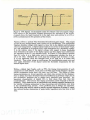
Figure 1. Discrete Vs. Integrated Circuits. Troubleshooting circuits built frorr
discrete components requires verifying relatively simple characteristics such as
resistance, capacitance, or turn-on voltages. Today's circuits built from digital
IC's require the verification of complex digital waveforms defined by the truth
table of the 1C.
I. ANALOG TECHNIQUES AND DIGITAL
TROUBLESHOOTING
When troubleshooting circuits built from analog components, the task is one of
verifying relatively simple characteristics such as resistance, capacitance, or
turn-on voltages of components with two or at most three nodes. While the
function of the total circuit may be quite complex, each component in that circuit
performs a relatively simple task and proper operation is easily verified. In Figure 1, each diode, resistor, capacitor and transistor can be tested using a signal
generator and a voltmeter, ohmmeter, diode checker, or oscilloscope—the traditional troubleshooting tools. But when this circuit is built in integrated circuit
form, these components are no longer accessible. It now becomes necessary
to test the operation of the complete circuit function.
Thus an important difference between discrete circuitry and today's circuits
built from digital IC's is in the complexity of the functions performed by these
new "components". Unlike the resistor, capacitor, diode or transistor, which
must be interconnected to form a circuit function, today's digital 1C performs
complete, complex functions. Instead of observing simple characteristics, it is
now necessary to observe complex digital signals and decide if these signals are
correct according to the function the 1C is meant to perform.
Verifying proper component operation now requires stimulating and observing
many inputs (in Figure 1 there are 10 inputs) while simultaneously observing
several outputs (often 2 or 3 and at times as many as 8). Thus another fundamental difference between circuitry built from discrete components and digital
IC's is the number of inputs and outputs associated with each component and
the need to stimulate and observe these simultaneously.
In addition to the problems of simultaneity of signals and complexity of
functions at the component level, the digital 1C has introduced a new degree
of complexity at the circuit level. Circuits which perplex all but their designer
are commonplace. Given enough time, these circuits can be studied and their
operation understood, but this is not an affordable luxury for those involved in
troubleshooting electronic circuits. Without understanding a circuit's intricate
operation, it becomes necessary to have a technique of quickly testing each
component rather than attempting to isolate a failure to a particular circuit
segment by testing for expected signals.
In order to solve these problems and to make the troubleshooting of digital circuits more efficient, it is necessary to take advantage of the digital nature of
the signals involved. Tools and techniques designed to troubleshoot analog
circuits do not take advantage of this digital nature and thus are less efficient
when used to troubleshoot digital circuits.
MARKETING
2.4V
Figure 2. TTL Signal. In the digital world, the relative value of a signal voltage
with respect to the threshold voltages determines the operation of the circuit.
A signal above the high threshold is in the high state and whether it is 2.8V or
3.0V is unimportant to the operation of the circuit.
Figure 2 shows a typical TTL (Transistor-Transistor-Logic) signal. This might
as well be any analog signal when viewed on an oscilloscope. The oscilloscope
displays absolute voltage with respect to time, but in the digital world absolute
values are unimportant. A digital signal exists in one of two or three states—high,
low, and undefined or in-between level—each determined hy a threshold voltage.
It is the relative value of the signal voltage with respect to these thresholds
that determines the state of the digital signal and this digital state determines
the operation of the 1C, not absolute levels. In Figure 2, if the signal is greater
than 2.4 volts, it is a high state and it is unimportant whether the level is
2.8 or 3.0 volts. Similarly for a low state the voltage must be below .4 volts.
It is not important what the absolute level is as long as it is below this
threshold. Thus when using an oscilloscope, the troubleshooter must over and
over again determine if the signal meets the threshold requirement for the
desired digital state.
Within a digital logic family, such as TTL, the timing characteristics of each
component are well defined. Each gate in the TTL logic family displays a characteristic propagation delay time, rise time, and fall time. The effects of these
timing parameters on circuit operation are taken into account by the designer.
Once a design has been developed beyond breadboard or prototype stage and is
into production, problems due to design have hopefully been corrected. An
important characteristic of digital IC's is that when they fail, they fail
catastrophically. This means that timing parameters rarely degrade or become
marginal. Thus observing on an oscilloscope and making repeated decisions on
the validity of timing parameters is time consuming and contributes very little
to the troubleshooting process. Once problems due to design are corrected,
the fact that pulse activity exists is usually enough indication of proper 1C operation without further observation of pulse width, repetition rate, rise time or fall
Figure 3. When stimulating a node in circuit, such as C above, it is necessary
to override the low impedance totem pole output stage driving that node.
When the output is in the low state, it is a saturated transistor to ground.
Presently used signal sources are not powerful enough to override this low state.
Figure 3 shows a problem created by the TTL logic family. The output stage of
a TTL device is a transistor totem pole. In either the high or low state, it is a
low impedance. In the low state it is a saturated transistor to ground. It thus
appears as 5—10 ohms to ground. This presents a problem to in-circuit stimulation. A signal source used to inject a pulse at a node which is driven by a
TTL output must have sufficient power to override the low impedance output
state. Most sources presently used for troubleshooting do not provide this
capability. It has been necessary for the troubles hooter to either cut printed
circuit traces or pull 1C leads in order to stimulate the circuit being tested.
Both of these practices are time consuming and lead to unreliable repairs.
Thus the use of the traditional oscilloscope and the traditional signal sources is
inefficient. Since the diodes and transistors are packaged in the 1C, use of diode
checkers is also marginal. These tools are general purpose tools that can be
applied to any situation if the trouble shooter has enough time. But with the
quantity and complexity of today's electronic circuits, it makes sense to find the
moat efficient solution to the problem at hand. This suggests using the oscilloscope, diode checkers and voltmeter on analog circuits where they really shine
and using instruments that take advantage of the digital nature of signals on
the digital circuitry to be repaired.
II. FAILURE MODES OF DIGITAL IC'S
In order to trouhleshoot efficiently, it is important to understand the type of
failures found in digital circuits. These can be categorized into two main
classes—those caused by a failure internal to an 1C and those caused by a failure
in the circuit external to the 1C.
There are four types of failures that can occur internally to an 1C. These are
(1) an open bond on either an input or output, (2) a short between an input or
output and Vcc or ground, (3) a short between two pins (neither of which are
Vcc or ground), and (4) a failure in the internal circuitry (often called the
steering circuitry) of the 1C.
In addition to these four failures internal to an 1C, there are four failures that can
occur in the circuit external to the 1C. These are (1) a short between a node and
Vcc or ground, (2) a short between two nodes (neither of which are Vcc or
TOOTHER 1C INPUTS
TO OTHER icINPUTS
SIGNALS AT POINTS A AND B:
1.4V TO 1.6V • "BAD LEVEL" AND
IS INTERPRETED BY TTL AND
DTL INPUTS AS A HIGH STATE
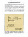
'igurc 4. The Effect of an Open Output Bond Upon Circuit Operation. An ope,
utput bond allows all inputs driven by that output to float to a "bad level.
This level is usually interpreted as a logic high state by the inputs. Thus the
inputs driven by an open output bond will respond as though a static logic high
signal utas applied.
Before discussing how to detect each of these failures we will discuss the effect
each has upon circuit operation. The first failure internal to an 1C mentioned
was an open bond on either an input or output. This failure has a different
effect depending upon whether it is an open output bond or an open input bond.
In the case of an open output bond (Figure 4), the inputs driven by that output
are left to float. In TTL and DTL circuits a floating input rises to approximately
1.4 to 1.5 volts and usually has the same effect on circuit operation as a high
logic level, Thus an open output bond will cause all inputs driven by that output
to float to a bad level since 1.5 volts is less than the high threshold level of
2.0 volts and greater than the low threshold level of .4 volt. In TTL and DTL,
a floating input is interpreted as a high level. Thus the effect will be that these
inputs will respond to this bad level as though it were a static high signal.
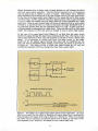
In the case of an open input bond (Figure 5), we find that the open circuit
blocks the signal driving the input from entering the 1C chip. The input on the
chip is thus allowed to float and will respond as though it were a atatic high
signal. It is important to realize that since the open occurs on the input
inside the 1C, the digital signal driving this input will be unaffected by the
open and will be detectable when looking at the input pin (such as at Point A
in Figure 5). The effect will be to block this signal inside the 1C and the
resulting 1C operation will be as though the input were a static high.
TOOTHER 1C INPUTS
TOOTHER 1C INPUTS
SIGNALS AT POINTS A AND B:
1.4V = "BAD LEVEL"
-IS INTERPRETED BY TTLINPUTS
A S A HIGH STATE
Figure 5. The Effect of an Open Input Bond Upon Circuit Operation. An open
bond on an input has the effect of blocking the input signal from reaching the
chip and allows the input of the chip to float to a "bad level." Thus even though
the signal can be viewed at an external point such as Point A, the input of the
chip responds to the "bad level" as though it were a static high level.
A short between an input or output and Vcc or ground has the effect of holding
all signal lines connected to that input or output either high (in the case of a
short to Vcc) or low (if shorted to ground) (Figure 6). In many cases, this will
cause expected signal activity at points beyond the short to disappear and thus
this type of failure is catastrophic in terms of circuit operation.
TOOTHER 1C INPUTS
TO OTHER 1C INPUTS
Figure 6. The Effect of a Short Between an Input or Output and Vcc or Gnd.
All signal lines connected to Point A are held in the high state. All signal
lines connected to Point B are held in the low state.
A short between two pins is not as straightforward to analyze as the short to Vcc
or ground. When two pins are shorted the outputs driving those pins oppose
each other when one attempts to pull the pins high while the other attempts to
pull them low (Figure 7). In this situation the output attempting to go high will
supply current through the upper saturated transistor of its totem pole output
stage while the output attempting to go low will sink this current through the
saturated lower transistor of its totem pole output stage. The net effect is
that the short will be pulled to a low state by the saturated transistor to ground.
Whenever both outputs attempt to go high simultaneously or to go low simultaneously, the shorted pins will respond properly. But whenever one output
attempts to go low the short will be constrained to be low.
IC1
—I—•)_
A
1C 2
TOOTHER 1C INPUTS
£D-
'
—i—v. B
TOO THER 1C INPUTS
Figure 7. The error effect of a short between two pins occurs when the outputs
driving those pins attempt to pull the short to opposite states. In this case,, the
output attempting to pull the node high wil
ill be supplying
hile the
be sinking the current. The saturated transistor to ground will thus pull th
node to a low state.
The fourth failure internal to an 1C is a failure of the internal (steering circuitry
of the 1C (Figure 8). This has the effect of permanently turning on either the
upper transistor of the output totem pole thus locking the output in the high
state or turning on the lower transistor of the totem pole thus locking the
output in the low state. Thus this failure blocks the signal flow and has a
catastrophic effect upon circuit operation.
STEERING CIRCUITRY
Figure 8. The Effect of a Failure of the Internal Circuitry of the 1C Upon
Circuit Operation. A failure of the steering circuitry of an 1C will either cause
the output to be in a static high state or a static low state.
A short between a node and Vcc or ground external to the 1C is indistinguishable
from a short internal to the 1C. Both will cause the signal lines connected
to the node to be either always high (for shorts to Vcc) or always low (for
shorts to ground). When this type of failure is encountered only a very close
physical examination of the circuit will reveal if the failure is external to the
1C.
Figure 9. The Effect of an Open in the Circuit External to an 1C. All inputs
attached to the node at Point A will be driven properly. Ail inputs to the
right of the open (Point B) will be left to float to a "bad level" and will therefore look like a static high state.
An open signal path in the circuit has a similar effect as an open output bond
driving the node (Figure 9). All inputs to the right of the open will be allowed
to float to a bad level and will thus appear as a static high level in circuit
operation. Those inputs to the left of the open will be unaffected by the open
and will thus respond as expected.
III. A DIGITAL TROUBLESHOOTING ALGORITHM
The first step in any troubleshooting process is to narrow the malfunctioning area
as much as possible by examining the observable characteristics of the failure.
This is often called "front panel milking." From the front panel operation (or
rather mis-operation) the failure should be localized to as few circuits as possible. At this point it is necessary to narrow further the failure to one suspected
circuit by looking for improper key signals between circuits. The Logic Probe can
be very effective here.*
In many cases, a signal will completely disappear. By rapidly probing the interconnecting signal paths, a missing signal can be readily detected. Another important failure is the occurrence of a signal on a line that should not have had a
signal. The Pulse Memory option for the Logic Probe allows such signal lines to
be monitored for single shot pulses or pulse activity over extended periods of
time. The occurrence of a signal will be stored and indicated on the Pulse
Memory's LED.
Dependence upon a well-written service manual is the key to this phase of
troubleshooting. Isolating a failure to a single circuit requires knowledge of
the instrument or system and its operating characteristics. A well written
manual will indicate key signals to be observed. The Logic Probe will provide
a rapid means of observing the presence of these signals.
Once a failure has been isolated to a single circuit, the 1C Troubleshooters (Logic
Probe, Pulser, Clip, Comparator) can be used to observe the effect of the failure
on circuit operation and to locate the failure to its cause (either an 1C or a fault
in the circuit external to the 1C). The technique described below for applying the
1C Troubleshooters to this task allows significant (4 to 1) improvements over
existing troubleshooting techniques by providing a digital solution to the digital
troubleshooting problem.
With today's circuits containing as many as several hundred IC's, the problem of
troubleshooting becomes one of physically isolating the trouble to the 2 or 3 IC's
affected by the failure. A majority of today's troubleshooting time is spent looking at signals which are good and determining that they are good. This is time
not spent solving the problem but rather time spent getting to the problem!
The Logic Comparator offers the opportunity to reduce drastically this time and
quickly to isolate the failure to only a few nodes out of the hundreds that exist
on a digital circuit thus allowing more time and talent to be spent analyzing the
trouble.
The first step in the troubleshooting algorithm (Figure 10) is to use the Logic
Comparator to test all testable IC's (see Appendix II for testable IC's) in the circuit or portion of the circuit which is suspected of failing and to note the IC's
and pins that the Comparator indicates as failing.** This will rapidly focus
attention on the physical areas of the circuit which are malfunctioning. Experience shows that this operation will require approximately 30 seconds per 1C.
" It is essential that the reader understand the operation of the Logic Probe,
Clip, Pulser, and Comparator; if not thoroughly familiar, the reader should
study Appendix I before proceeding.
'"Often, the sensitive Logic Comparator indicates a failure because its clip is
not making good contact especially when the IC's have been sprayed with a
sealer. Thus before deciding that a node definitely does not compare, squeeze
the clip's jaws tightly and apply a slight twisting motion.
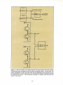
STEP 1. Test all IC's using the Ixigic C
alor or Logic Probe. Pulser and Clip a
the failing nodes.
STEP 3. Test for a short to Vcc or GND using
the Ugic Pulser and Probe. By simultaneously probing and pulsing the had node a short
to Vec or GND can be detected since the
Pulser is unable to inject a pulse into such
a short.
STEP 4. Test for a short between two nodes
using the Logic Probe and Pulser or an
Ixigic Probe. If an
replace the 1C
STEP 5. If the failure is not found in steps 2
thru 4 then the failure is either an open
input bond or a failure of the internal circuitry of the 1C driving the failing node,
fn either rase thp 1C driving the failing node
should be replaced.
Figure 10. Digital Troubleshooting Algorithm. After Step 1, the mapping step,
the LOGIC PROBE, and PULSER are used to eliminate systematically the causes
of 1C failures discussed in Chapter III. In Step 5 the cause is determined by
induction from the results of Steps 2 through 4,
For those IC's that are not testable with the Logic Comparator or for which a
reference card does not exist, the Logic Probe, Pulser, and Clip can be used to
verify proper 1C operation. The Logic Probe can be used to observe the signal
activity on inputs and to view the resulting output signals. Prom this information, a decision can be made as to the proper operation of the 1C. For example,
if a clock signal is occurring on a decade counter and the enabling inputs
(usually reset lines) are in the enabled state then the output should be counting.
The Logic Probe will allow the clock and enabling inputs to be observed, and,
if putse activity is indicated on the outputs, then the 1C can be assumed to be
operating properly. As stated before, usually it is not necessary to see the actual
timing of the output signals since IC's fail catastrophically. The occurrence of
pulse activity is often enough indication of proper operation.
When more detailed study is desired or when input signal activity is missing,
the Logic Pulser can be used to inject input signals and the Logic Clip or Probe
used to monitor the response. This technique is especially good when testing
digital gates and other combinatorial devices. The Logic Pulser can be used to
cause the inputs to go to a state which will cause a change in the output state.
For example, a three-input NAND gate which has high, low, low inputs will have
a high output. By pulsing the two low inputs high using the Logic Pulser (and
the Multi-pin Stimulus Kit, if necessary) the output will pulse low and can be
detected by the Logic Probe. This then indicates that the 1C is operating
properly. The Logic Pulser is also valuable for replacing the clock in digital
circuit thus allowing the circuit to be single-stepped while the Logic Probe and
Clip are used to observe the changes in circuit's state.
This first step might be called the "mapping" step aince the effect is to map
out the problem areas for further investigation. It is important to do a complete
"mapping" of the circuit before proceeding to analyze each of the indicated
failures. Prematurely studying a fault can result in overlooking of faults which
cause multiple failures such as shorts between two nodes. This then often leads
to the needless replacement of a good 1C and much wasted time. With a complete trouble-area "map" we can begin to determine the type and cause of the
failures. We do this by systematically eliminating the possible failures of
digital circuits discussed above.
The first failure to test for is an open bond in the 1C driving the failed node.
The Logic Probe provides a quick and accurate test for this failure. If the output
bond is open, then the node will float to a bad level. By probing the node, the
Logic Probe will quickly indicate a bad level. If a bad level is indicated then the
1C driving the node should be replaced and retested with the Logic Comparator.
If the node is not a bad level then a test for a short to Vcc or ground should
be made next. This can be done easily using the Logic Pulser and Probe.
While the Logic Pulser is powerful enough to override even a low impedance
TTL output it is not powerful enough to effect a change in state on a Vcc or
ground bus. Thus if the Logic Pulser is used to .inject a pulse while the
Logic Probe is used simultaneously on the same node to observe the pulse, a
short to Vcc or ground can be detected. The occurrence of a pulse indicates
that the node is not shorted, and the absence of a pulse indicates the node is
shorted to Vcc (if it is a high) or ground (if it is a low).
If the node is shorted to Vcc or ground there are two possible causes. The first
is a short in the circuit external to the IC's and the other is a short internal
to one of the IC's attached to the node. The external short should be detected by
an examination of the circuit. If no external short is found then the cause is
equally likely to be any one of the IC's attached to the node. The only suggestion
that can be made (based upon experience) is to first replace the 1C driving the
node and if that does not solve the problem try each of the other IC's individually
ponents such as resistors or capacitors attached to the node have shorted.)
If the node is not shorted to Vcc or ground nor is it an open output bond then
we should look for a short between two nodes. This can be done in one of two
ways. First the Logic Pulser can be used to pulse the failing node being
studied and the Logic Probe can be used to observe each of the remaining failing
nodes. If a short exists between the node being studied and one of the other
failing nodes, then the Pulser will cause the node being probed to change state
(i.e., the Probe will detect a pulse). To ensure that a short exists, the Probe and
Pulser should be reversed and the test made again. If a pulse is again detected
then a short is definitely indicated. As a further test or as another way of
testing for a short between two nodes, the circuit can be removed from the instrument or system and an ohmmeter can be used to measure the impedance
between the two failing nodes. A short between them will be easily detected.
If the failure is a short then there are two possible causes. The most likely
is a problem in the circuit external to the IC's. This can be detected by physically
examining the circuit and repairing any solder bridges or loose wire shorts found.
Only if the two nodes which are shorted are common to one 1C can the failure
be internal to that 1C. If after examining the circuit no short can be found
external to the 1C, then the 1C should be replaced.
If the failure is not a short between two nodes then there are only two possibilities left. They are that the failure is an open input bond or a failure of
the internal circuitry of the 1C that the Comparator indicates has failed. In
either case, this 1C should now be replaced. Thus, by systematically eliminating
the 1C failures, the cause can be located.
An important step at any point where an 1C is replaced is the retesting of the
circuit with the Logic Comparator. If the Comparator again indicates a
ore study
suy of
o thee problem
p r o e m must
mus bee made
mae with the knowledg
failure, then more
that the failur is not in the 1C that has just been replaced.
There is e type of failure that was not discussed in the algorithm, and that
is an open signal path in the circuit external to the 1C (Figure 11). This type
of failure will not be indicated by the Logic Comparator and will therefore
not be shown on the trouble-area map. If after using the Logic Comparator to
test all the IC's, no nodes are indicated as failing, or, if after finding the
cause of the failures indicated by the Logic Comparator, the circuit is still
malfunctioning, then an open signal path can be suspected.
Figure 11. The Effect of an Open Signal Path External to the IC's. The open
causes Point B to float to a bad level while Point A is driven by proper TTL or
DTL signal levels. Starting at the input of gate 3 or 4 and proceeding back toward
gate 1, the exact location of the open can be determined using the Logic Probe.
The Ix>gic Probe provides a rapid means of not only detecting but also physically
locating the open. Since an open signal path allows the input to the "right"
of the open to float to a bad level, the Logic Probe can be used to test the
input of each 1C for a bad level. Once an input floating at a bad level is
detected, the Logic Probe can be used to follow the circuit back from the input
looking for the open. This can be done because the circuit to the "left" of the
open will be a good logic level (either high, low, or pulsing) while the circuit
to the right will be a bad level. Thus probing back along the signal path will
indicate a bad level until the open is passed. Thus the Probe can be used to
locate precisely the open. The open can then be repaired and the circuit tested.
This systematic elimination of possible failures in digital circuits coupled with
the digital 1C Troubleshooters will ensure a rapid and accurate repair. Because
the 1C Troubleshooters provide a digital solution to the digital problem, improvements in troubleshooting time of at least 4 to 1 are easily achieved.
APPENDIX I. THE 1C TROUBLESHOOTERS—
A DIGITAL SOLUTION
The LOGIC PROBE is a digital state (highs and lows) indicator which provides
at the user's fingertips an indication of a high level, low level, or bad level
signal. Internal threshoid detectors determine if the signal being probed is above
the high threshold level {see Figure Al), below the low threshold level, or inbetween these two. A lamp indicator then glows brightly for a high level,
goes off for a low level, and glows dimly for a signal that is between the two
thresholds.
levels described above, the LOGIC PROBE also has pulse stretching circuitry
which detects pulses as narrow as 10 ns and stretches them to give a .1 sec blink
of the lamp indicator. Thus if a low signal pulses high, the LOGIC PROBE
will blink "ON" and if a high signal pulses low, it will blink "OFF." When
the PULSE MEMORY OPTION is used with the LOGIC PROBE, monitoring of
a signal line for single shot or low frequency pulses over extended periods of time
is possible. An L.E.D. in the Pulse Memory will light upon the occurrence of a
pulse and will remain on until reset by the user.
In addition to single shot pulses, the LOGIC PROBE will also indicate pulse
trains of frequencies up to 50 MHz. It does this by blinking the lamp indicator
at a constant 10 Hz rate.
SPECIFICATIONS:
Logic Probe
Input Impedance: >2.ri kn in both the high and low state.
Logic One Threshold: 2.0V ± 0.2V.
Input Minimum Pulse Width: 10 ns (S ns typical).
Input Maximum Pulse Repetition Frequency: >50 MHz.
Input Overload Protection: *70 volts continuous, ±200 volts intermittent,
120V ac for 30 seconds.
Power Requirements: 5V ± 10% at 100 mA, internal overload protection fo
voltages from +7 to -IS volts. Includes power lead reversal protection.
Temperature: 0° to 55°C.
Accessories Included: BNC to alligator clips, ground clip.
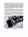
Figure Al. I0525T Logic Probe.
Thus the LOGIC PROBE allows the user to view static signals, single shot pulses,
and pulse trains at his finger tip. Automatic threshold detection eliminates the
need to determine repeatedly if a signal is above or below the threshold.
The response of the lamp indicator is so intuitively related to the actual signal
activity that interpretation is rapid and simple.
The LOGIC CLIP is another digital state indicator (Figure A2). It allows up to
16 signals on a single 1C to be observed simultaneously. The LOGIC CLIP has
a single threshold level. If a signal on a given 1C pin is above this level,
an LED in the CUP is turned on corresponding to that pin. If the signal is
below this level the LED is turned off. Thanks to internal power seeking
circuitry, the LOGIC CLIP cannot be attached improperly. Regardless of how it
is clipped onto the 1C, it will display the desired signal.
The LOGIC CLIP differs from the LOGIC PROBE in two important ways. First,
it has a single threshold as opposed to the two threshold in the LOGIC PROBE
and will therefore not indicate a bad level. It will respond to a bad level
signal in the same way a TTL or DTL gate will, as a logic high state. Secondly
the LOGIC CLIP does not have pulse stretching circuitry. In order to view high
frequency or single shot narrow pulses, the LOGIC PROBE should be used.
1052SA LOGIC CLIP
SPECIFICATIONS:
Logic Clip
Input Threshold: 1.4 ± 0.6V; TTL or DTL compatible (except gates with
expander inputs).
Input Impedance: One TTL load (-1.2 mA typical per input).
Input Protection: Voltages < -IV or >7V must be current limited to 10 mA.
Supply Voltage: 5V ± 10% across any two or more inputs.
Maximum Current Consumption: 120 mA.
Temperature: 0° to 65°C.
Dimensions: 2.15 in. high, 1.5 in. wide, 1 in. deep (55 x 40 x 25 cm), maximu
Weight: Net, 1.5 oz. (45 gm). Shipping, 4 oz. (120 gm).
Figure A2. 10528A Logic Clip. With the Logic Clip, up to 16 signals on a given
1C can be observed simultaneously. Internal power seeking circuitry allows the
clip to be attached in any orientation and makes its operation completely
portable.
-18-
The ability to view signal activity on several pins simultaneously is a tremendous
time saver. Consider the problem of testing a decade counter (e.g., 7490). It
is necessary to view at least one input and four outputs simultaneously to
determine if this device is operating properly. With the LOGIC CLIP this is no
problem.
The LOGIC PROBE and CLIP provide a response mode of operation to the user
that is optimized to digital signals. But the mainstay of all troubleshooting is
stimulus-response testing. It is necessary to apply a signal and observe the
response to determine if the device is operating properly. As was pointed out
previously, this is very difficult to do in TTL circuits.
The LOGIC PULSER provides the solution in an easy to use probe package
(Figure A3). The LOGIC PULSER injects into the circuit a single 300 ns wide
pulse of proper amplitude and polarity each time its button is pushed. If the
node was low, it will be pulsed high and if it was high it will be pulsed low
without the need to readjust the PULSER. The PULSER is capable of sourcing
or sinking .75A for the 300 ns pulse width to ensure that the node is pulsed.
The narrow width (300 ns) will not damage the IC's being pulsed.
Thus it now becomes possible to jump rapidly from point to point in the circuit
applying pulses and observing the responses. Together the LOGIC PULSER,
LOGIC PROBE and LOGIC CLIP provide total in-circuit stimulus response testing for all TTL families, DTL, and other 5 volt logic.
SPECIFICATIONS:
Output
Output
Output
Output
Logic Falser
HIGH Pulse Voltage: >2V at .65A (1A typical at Vps - 5V, 25°C).
LOW Pulse Voltage: <0.8V at .65A (1A typical at Vps = 5V, 25°C).
Impedance, Active State: <2 ohms.
Impedance, Off State: >1 Megohm.
Pulse Width: 0.3 ii-.~ nominal.
Input Overload Protection: ±50 volts continuous.
Power Supply Input Protection: ±1 volts (includes power lead reversal protection).
Power Requirement: 5V - 10% at 25 mA.
Temperature: 0°C to 55°C.
Accessories Included: BNC to alligator clips, ground clip.
Figure A3. 10526T Logic Pulser. The Logic Falser provides a solution to the
indrcuit stimulus problem of TTL and DTL circuits. Nodes are automatically
pulsed from their current digital state to the opposite state for 300 ns with the
press of a finger.
While stimulus-response testing is the mainstay of electronic troubleshooting,
the digital nature of the signals of the circuit being tested allows for an even
parison testing. By stimulating a known good device with the same signals
as used to stimulate the device under test and comparing the response of the
two components, one can verify that the device under test is operating properly.
This is exactly what the 10529A LOGIC COMPARATOR does. For the TTL and
DTL logic families, the COMPARATOR steals the input signals stimulating the
device under test to stimulate simultaneously a known good device. Any difference in their response is indicated by an "ON" LED corresponding to the
output which failed the comparison.
The 10529A LOGIC COMPARATOR has pulse stretching circuitry which allows
dynamic, single shot or intermittent errors to be detected and displayed as
well as static errors. Errors as short as 200 ns are detected and displayed
as a .1 sec blink on the LED display. This means the most difficult type of
error possible, intermittent failures, will be easily detected and displayed.
The COMPARATOR removes the burden of analyzing long, complex digital
signals from the troubleshooter by automatically determining if the signal is a
good "high" or "low" level and if that level is correct according to the expected
truth table of the circuit being tested. Thus, the LOGIC COMPARATOR
vastly reduces troubleshooting time. (See Appendix II for more details on the
LOGIC COMPARATOR.)
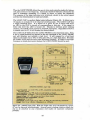
10529A Logic Comparator.
COMPARATOR RESPONSE TO ERRORS
SPECIFICATIONS: Logic Comparator
Input Threshold: 1.4V nominal, TTL or DTL compatible.
Test 1C Loading: Outputs driving Test 1C inputs are loaded by 2 low-power TTL loads
plus input of Reference 1C. Test 1C outputs are loaded by 1 low-power TTL load.
Input Protection: Voltages <-lV or >7V must be current limited to 10 mA.
Supply Voltage: 5V - 10%.
Supply Protection: Supply voltage must be limited to TV.
Maximum Current Consumption: 300 mA.
Sensitivity: Error Sensitivity: 200 ns. Errors' greater than this are detected and
stretched to at least 0.1 second. Delay Variation Immunity: 50 ns. Errors shorter
than this value are considered spurious and ignored.
Frequency Range: With a 50% clock duty cycle, max, frequency is typically 2.5 MHz.
Temperature: 0°C to 55°C.
Dimensions: 1.4 in. deep, 3.375 in. wide, 7.15 in. long (3,56 x 8, 55 x 10,2 cm).
Weight: Net, 2 Ib. 6 on. (1,14 kg); Shipping, 3 Ib. 6 oz. (1,62 kg).
Accessories Included: 1 teat board; 10 blank reference boards; 1 carrying case.
Figure A4.
10529A Logic Comparator.
The Logic Comparator uses the test
card. The resulting output signals are compared and any differences longer
than 200 ns are displayed on the corresponding LED in the Logic Comparator.
COMPARATOR RESPONSE TO ERRORS
SPECIFICATIONS: Logic Comparator
Input Threshold: 1.4V nominal. TTL or DTL compatible.
Test 1C Loading: Outputs driving Test 1C inputs are loaded by 2 low-power TTL loads
plus input, of Reference 1C. Test 1C outputs are loaded by 1 low-power TTL load.
Input Protection: Voltages <-lV or >7V must be current limited to 10 mA.
Supply Voltage: 5V ± 10%.
Supply Protection: Supply voltage must be limited to TV.
Maximum Current Consumption: 300 mA.
Sensitivity: Error Sensitivity: 200 ne. Errors' greater than this are detected and
stretched to at least fl.t second. Delay Variation Immunity: 50 ns. Errors shorter
than this value are considered spurious and ignored.
Frequency Range: With a 50% clock duty cycle, max. frequency is typically 2.5 MHz.
Temperature: 0"C to 55°C.
Dimensions: 1.4 in. deep, 3.375 in. wide, 7.15 in. long (3,56 x 8, 55 x 10,2 cm).
Weight: Net, 2 Ib. 6 OK. (!,14 kg); Shipping, 3 Ib. 6 oz. (1,62 kg).
Accessories Included: 1 test board; 10 blank reference boards; 1 carrying case.
Figure A4. 10529A Logic Comparator. The Logic Comparator uses the test
circuits signals to stimulate a reference 1C which is mounted on a reference
card. The resulting
suiting output signals are compared and any differences lo,
longe,
J
L
J
TT
than 200
'•'--'
— 'the
~- 'LED
'" *"in ""
'e displayed
on
corresponding
the '----Logic •"Compare
APPENDIX II. WHAT WILL THE 10529A LOGIC
COMPARATOR TEST?
Before discussing what the COMPARATOR will test, it is important to understand how it works. Through a reference board, the inputs of a reference 1C
are connected to the inputs of the test 1C (Point A in Figure A4), thus the
reference 1C is exercised by the same signals that stimulate the test 1C. The
outputs of the reference and test 1C are compared (Point B in Figure A4) and any
differences greater than 200 nsec in duration signal a failure. Also the reference 1C and the COMPARATOR are powered by the circuit under test through
the reference board. Thus, the LOGIC COMPARATOR observes simultaneously
all outputs of the test 1C and determines the validity of these signals based
both upon proper voltage levels and proper truth table response to the input
An important consideration in using the LOGIC COMPARATOR is circuit
loading. The loading considerations can be divided into two parts. The first is
the type of load the COMPARATOR presents to the outputs of the 1C to which
the COMPARATOR is attached and the second is the load presented to the
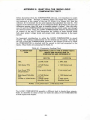
inputs. These loads are summarized in Table Al.
Table Al. Comparator Loading Chart
1C UNDER TEST
TYPE
ADDITIONAL LOAD TO THE 1C UNDER TESTS
INPUTS AND OUTPUTS DUE TO
COMPARATOR AND REFERENCE 1C
INPUTS
OUTPUTS
DTL
1.2 DTL loads
.1 DTL load
7400 Series TTL
1.2 7400 Series
loads
.17400 Series load
Low Power TTL
(74LOO Series)
5 low power loads
1 low power load
High Speed/Schottky
TTL
(74HOO or 74SOO Series)
1.5 7400 Series
loads or
1.2 high speed/
Schottky loads
.1 7400 Series load
.1 high speed/
Schottky loads
NOTE: 1 low power load = .1 7400 Series load.
The LOGIC COMPARATOR presents a different load to inputs than outputs.
Table Al describes in terms of fan out loads the affect of the COMPARATOR
on both inputs and outputs.
Under most conditions, this additional loading will not affect the circuit
operation. One major exception is when analog components, such as R's, C's,
or transistors are used to control circuit timing or to buffer signals (see Figure A6). Since the COMPARATOR loads these circuits as described above, the
timing or drive capability of the circuit may be affected. This loading should
be considered when testing these circuits.
Figure A5. The "Open Collector" Problem, When gates are connected in the
"wired-OR" arrangement, the output of one 1C can constrain the outputs of
the other IC's to be in a state other than that defined by the gates truth table
and input states.
One problem faced by all troubleshooting instrumentation is what is fondly
called the "open-coHector evil." In the family of TTL IC's there is a sub-family
called "open-collector" gates. These are circuits whose outputs can be tied
together (sometimes called "wire-ORed" or "wire-AND") such that one circuit's
output can constrain the other circuits' outputs to be in a given state regardless
of their inputs. For example, gates A, B, and C are "wire-ORed" together.
Under certain conditions gate A's output can cause gates B's and C's outputs to
be a TTL low regardless of their input state. Thus from a truth table point of
view the gates B and C are constrained to operate improperly.
This then is the "open-coHector evil." Because the COMPARATOR tests for
output states according to the truth table of the test 1C, a fault will be indicated
when the output is constrained as described above. Using conventional instrumentation such as voltmeters and oscilloscopes does not solve this problem
either. When a problem is thought to be caused by "open collector" gates, the
usual solution is to replace the gates one at a time until the problem is solved
or to unsolder the outputs and to test the IC's individually. The COMPARATOR
can be used if this last technique is followed.
A33 LflMP DRIVERS ASSEMBLY «
Figure A6. Analog components used to control circuit timing or to buffer signals
may be loaded by the Logic Comparator. Care should be taken in testi g these
The class of integrated circuits known as sequential integrated circuits presents today's troubleshooters with many difficult problems. IC's such as memories, shift registers, and flip-flops whose present outputs depend on previous
inputs are called sequential IC's. Testing these devices with conventional tools
requires the observation and study of the relationship of several waveforms. In
some cases these waveforms are long and complex and verification of proper
1C operation is practically impossible. The 10529A LOGIC COMPARATOR,
when used properly, provides a very efficient and simple solution to troubleshooting these IC's.
Since the operation of a flip-flop or other sequential device depends upon the
previous input to that device, and since the reference device will not in general
have had the same "prior" set of inputs as the device being tested, it is necessary to "reset" the devices before comparing. This can be done by first clipping
the COMPARATOR to the device to be tested and causing a reset signal to be
supplied by either the circuit to be tested or the 10526T LOGIC PULSER. The
PULSER can be uaed to inject a reset pulse into the IC's reset input. This then
ensures that both devices start in the same state and will react the same to the
sequence of input signals they receive. The COMPARATOR will now flip and
not flop when the flip-flop flips. If the test 1C is good, the output states of the
reference and test 1C will always agree and the COMPARATOR will not indicate
a fault. In some cases the reset lines are connected directly to Vcc or ground
and are thus not pulseable. In this case turning power off and back on sometimes brings both the test 1C and the reference 1C up to the same state.
With memories and shift registers, the problem is quite similar as stated above.
But instead of supplying a reset pulse to the circuit to bring them to a known
state, the COMPARATOR must merely be attached to the test 1C long enough for
the reference 1C to be loaded with the same data as the test 1C. This should
require no longer than 1 complete cycle of the memory or shift register.
During the time the reference 1C is being loaded with the data, the COMPARATOR will give fault indications. If after a few cycle times the fault is still
indicated, a fault has indeed occurred at the node indicated.
The 10529A LOGIC COMPARATOR provides rapid, incircuit testing of TTL integrated circuits. While the vast majority of these devices are easily testable
with the COMPARATOR, some devices require special consideration and some
are not testable. Table A2 is meant to be a quick reference to help the digital
troubleshooter decide upon the testability of a given component in the 54/7400
series TTL family. (The 5400 and 7400 numbers are often used to refer to the
set of devices with a 54 or 74 prefix.) This is not meant to be an exhaustive list
of TTL or even 54/7400 devices, but rather a quick reference for the most
widely used devices.
As a general summary of the LOGIC COMPARATOR'S capabilities, Table A3
describes applicability of the COMPARATOR to general digital devices. While
the 10529A LOGIC COMPARATOR is not a total solution, as indeed no single
instrument is, it is the most powerful digital troubleshooting tool available
in a world that is rapidly changing from analog to digital electronics.
Table A3. 54/7400 Testability Chart*
54/7400 TESTABILITY CHART"
T - TESTABLE; OT - OFTEN TESTABLE; NT = NOT TESTABLE
T OT NT NOTE
T OT NT .NOTE
7445
X
7487
7400 X
r-ioi
I
7446
X
2
7488
7447
X
X
7489
1
7448 X
7490
X
7449 X
74(J2
X
1
7450
7433
X
2
1
7451 X
X
7494
X
1
7452
2
7495
X
7453
X
7496
X
X
7454 X
7497
X
7455
2
X
7498
7460
X
X
2
7-1 [DO
X
74fll
7462
x
X
7464 X
74X02
X
1
7465
1
7-110.3
X
X
1
3
7410-1
7470 X
X
3
X
7471 X
T4XOS
X
7472 X
3
74X06
7 11)7
1
7473 X
X
3
7 IDS
X
2
7474 X
4
X
7475 X
4
7 1 1
X
2
7476 X
3
7 12
7477 X
X
4
?.! l i t X
741 :)
7478 X
3
741 4
7.1 >.' X
7480 X
74121
7-437 X
7481 X
7I3S
X
1
7482 X
74122
7.! 10 X
7483 X
74123
7-142 X
7484 X
74141
7443 X
7485 X
74145
7444 X
7486 X
74150
7-102
7-!0>
710-1
. !!J.j
', !or,
7407
7408
T !i> ;
74 0
74 1
7-1 2
74 3
74 5
74 6
74 7
7420
7-1211
7. i?: .
7423
7 t '..7426
7427
OT M NOTE
x
x
x
X
X
X
X
OT VT NOTE
5
6
8
8
8
6
6
6
8
6
74151
74152 ;
74 1 5 5
7415-1
7-1 1 55 t
74156
74 Kill
74161 .
7-1JCS2
741(0 i
741B4
4
74166
3
3
3
3
3
3
3
74170
74180
74LS2
741 S3
7IIS-1
71IS5
,
.
?
^
3
3
3
3
7
7
7 1 1 <)[
7I!')2
7-fl'J.i
7-1 I ' l l
7)]'o
711'jl,
>
.
•>
."
>
>
2
2
74X98
74199 ?
x
1
8
8
8
8
6
6
X
1
7 mi .
8
8
8
8
6
6
8
8
6
6
Testable when not "wjre-or'ed" (i. ., .several outpu s wired together),
2. Device willi iioiicmnp tible input ur output signal!; (i.e.. ex
ilile gates, Nixie drivers).
3. JK flip-flop-if J = K = high or low, thru referent.-*: 1C ant 1C under lest m y be out of phase. Pulse
set ur dear or random y ^e J ^ K'
ei u n tr()ull,(,
4. D vpu or latch flip-flc
5. ROM-no trouble.
6. RAM. shift refiisU'r-i mparafor must 1)0 attached long en
1C and 1C under test <o
IK- luiidi'fl «'Uh SJim- (
7. MuiiiJSlabk-circiiit tir ling may ie affected.
nized. Pulse set or clear
input.
Table A3. Comparator Capabilities Chart
(16 or Less Pin Dual-in-Line DTL, TTL)
(AND, NAND,
XOR, etc.
Excellent. This also includes expandable IC's.
This category includes the vast majority of
IC's in use.
Sequential Logic
(Flip-Flops)
Excellent. Reference and test 1C must be
synchronized by a pulse on the "Reset" input.
Memories, Shift
Registers
Excellent. Clip must be attached long enough
for reference and test 1C to contain the same
information.
law Power TTL
Good. The Comparator is an in load of 5
for the driving device.
One-shots
Usually good. Since reference and test 1C
share the RC timing components, circuit
timing will be affected.
Open collector and
Tri-state Logic
Usually poor. When outputs are bussed
together a good gate is constrained to operate
improperly and this will be indicated by the
Comparator.
Expanders, Analog
and Linear IC's
No. Their outputs are analog and cannot be
tested by the Comparator.
MOS Devices
No. They require different power supplies
exceeding the TV input limit and will
damage the Comparator.
HEWLETT-PACKARD
e, Posl Wli« Bm »S, CH-1217 Mtyrin !. Oi
PRINTED IN U.S.A.