1
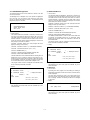
SERVICE MANUAL
CODE: 00ZERA750USME
MODEL ER-A750
(For "U" & "A" version)
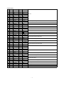
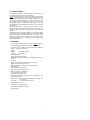
CONTENTS
CHAPTER 1.
SPECIFICATIONS . . . . . . . . . . . . . . . . . . . . . . . . . . . . . . . . . . . . . . . . . . . . . . . . .1-1
CHAPTER 2.
OPTIONS . . . . . . . . . . . . . . . . . . . . . . . . . . . . . . . . . . . . . . . . . . . . . . . . . . . . . . . .2-1
CHAPTER 3.
SERVICE PRECAUTION . . . . . . . . . . . . . . . . . . . . . . . . . . . . . . . . . . . . . . . . . . .3-1
CHAPTER 4.
SRV RESET (Program Loop Reset) and switch to SRV mode . . . . . . . . . . . . . .4-1
CHAPTER 5.
MASTER RESET . . . . . . . . . . . . . . . . . . . . . . . . . . . . . . . . . . . . . . . . . . . . . . . . . .5-1
CHAPTER 6.
DIAGNOSTICS
CHAPTER 7.
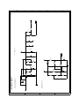
CIRCUIT DESCRIPTION . . . . . . . . . . . . . . . . . . . . . . . . . . . . . . . . . . . . . . . . . . . .7-1
CHAPTER 8.
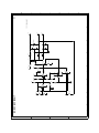
PWB LAYOUT . . . . . . . . . . . . . . . . . . . . . . . . . . . . . . . . . . . . . . . . . . . . . . . . . . . .8-1
CHAPTER 9.
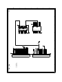
CIRCUIT DIAGRAMS . . . . . . . . . . . . . . . . . . . . . . . . . . . . . . . . . . . . . . . . . . . . . . .9-1
. . . . . . . . . . . . . . . . . . . . . . . . . . . . . . . . . . . . . . . . . . . . . . . . . .6-1
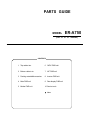
PARTS GUIDE
Parts marked with "!" is important for maintaining the safety of the set. Be sure to replace these parts with specified ones for
maintaining the safety and performance of the set.
SHARP CORPORATION
This document has been published to be
used for after sales service only. The contents are subject to change without notice.
TheRBRCTM Seal
The RBRCTM Seal on the easily removable nickel-cadmium battery pack contained
in our product indicates that SHARP is voluntarily participating in an industry program to
collect and recycle these battery packs at the end of their useful life, when taken out of
service within the United States. The RBRCTM program provides a convenient alternative to
placing spent nickel-cadmium battery packs into the trash or municipal waste stream,
which is illegal in some areas.
SHARP’s payments to RBRCTM makes it easy for you to drop off the spent battery pack at local retailers of
replacement nickel-cadmium batteries, or at authorized SHARP product service centers. You may also contact
your local recycling center for information on where to return the spent battery pack. SHARP’s involvement in this
program is part of its commitment to protecting our environment and conserving natural resources.
(RBRCTM is a trademark of the Rechargeable Battery Recycling Corporation.)
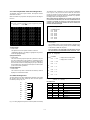
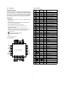
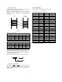
3. Keyboard
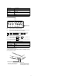
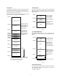
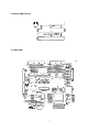
CHAPTER 1. SPECIFICATION
1) Standard keyboard layout
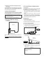
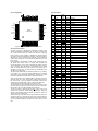
1. Apearance
External view
Front view
Operator display
91
92
93
94
95
96
97
82
83
84
85
86
87
88
AC cord
Power switch in
sure that the power
switch is placed in the
OFF position prior to
connecting AC power
Left side of
the machine
LEVEL LEVEL LEVEL LEVEL
2
3
4
5
89
TEX1
SHIFT
TEX2
SHIFT
AUTO
1
MODE
EMP
#
AUTO
2
DRV
NC
BAL
RFND
DRV
GLU
73
74
75
76
77
78
79
80
81
64
65
66
67
68
69
70
71
72
RCPT
55
56
57
58
59
60
61
62
63
48
47
49
50
51
52
53
MISC
FUNC
90
RP
SEND
46
Keyboard
LEVEL
1
1
%1
RTN
SRVC
54
NDSE
SBTL
CHK
#
CH
#
FINAL
PAST
VOID
SBTL
VOID
PLU/
SUB
TRAY
SBTL
38
39
40
41
42
43
44
45
VOID
30
31
32
33
34
35
36
37
PA GE
UP
SE RV
#
@/
FOR
CL
$5
PA GE
DOWN
7
4
1
0
8
5
2
00
9
6
3
$10
22
23
24
25
26
27
28
29
14
15
16
17
18
19
20
21
7
8
9
10
11
12
1
2
3
4
5
6
CANCEL
ENTER
13
$20
SBTL
CA/AT
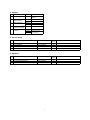
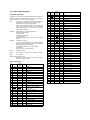
2) Key top name
1 Standard key top
KEY TOP
0 ∼ 9,00
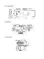
IR receiver cover
Brightness
control
Contrast control
•
Decimal point key
CL
Clear key
@/FOR
RCPT
RP SEND
Rear view
Customer
Display
Percent 1 key
Refund key
VOID
Void key
PASTVOID
Past void key
SBTL VOID
Subtotal void key
LEVEL 1 ∼ 5
Weight
11.2 lbs. (5.1 kg)
PLU level shift 1 ∼ 5 keys
Service key
Final key
Balance key
DRV NC
New check 2 key (For drive-through)
DRV GLU
Gest look up 2 key (For drive-through)
SERV#
Server code entry key
EMP#
Employee code entry key
Power source
120V AC ± 10% 60 Hz
MODE
Power consumption
Stand-by: 22W
Operating: 25W (max.)
AUTO1,2
ENTER
1–1
Price lookup / Subdepartment key
Direct price look up key
FINAL
MISC FUNC
Working temperatures 32 to 104˚F (0 to 40˚C)
Return key
SRVC
BAL
11.4 × 14.4 × 10.3 in. (290 × 365 × 262
mm)
Tax 1 and 2 shift keys
RFND
1 ∼ 99
External dimensions
Remote printer send key
%1
PLU / SUB
2. Rating
Receipt print key
Discount 1 key
RTN
Power switch
Multiplication / Split-pricing key
d1
TAX1SHIFT
TAX2SHIFT
Rear cover
DESCRIPTION
Numeric keys
Miscellaneous function key
Mode key
Enter key
Automatic sequencing 1 and 2 keys
CH#
Charge menu key
CHK#
Check menu key
TRAYSBTL
Tray subtotal key
MDSE SBTL
Merchandise subtotal key
KEY TOP
DESCRIPTION
SBTL
Subtotal key
CA/AT
Cash / Amount tendered key
$5,$10,$20
PAGE UP
KEY TOP
Page up key
Page down key
→
Cursor right key
Scale entry key
3) Text programming key sheet layout
Speed tender key
(Used for AUTO8,9,and 10 key)
PAGEDOWN
DESCRIPTION
SCALE
[
]
~
N
_
,,
+
,
←
Cursor left key
!
@
#
$
%
^
&
*
(
↑
Cursor up key
Q
W
E
R
T
Y
U
I
O
↓
CANCEL
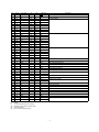
2 Optional key top
Cursor down key
A
Cancel key
(SHIFT)
KEY TOP
000
98 ∼ 135
1 ∼ 50
Transfer out key
Cash tip key
DEPOSIT
DEPOSITRF
TAX
GRT EX
COVER CNT
BILL
CONV#
SHIFT1 ∼ SHIFT5
BACKSPACE
DELETE
NC
GLU
Charge tip key
Tip paid key
Eat in 1 ∼ 3 keys
Tax 3 and 4 shift keys
Deposit key
Deposit refund key
Manual tax key
Gratuity exempt key
Cover count entry key
Bill print key
Currency conversion menu key
Price level shift 1 ∼ 5 keys
Backspace key
Delete key
New check key
Guest look up key
#
Non-add code entry key
NS
No-sale key
MGR#
OPENTARE
REPEAT
PERSON#
IND.PAYMENT
EMPL.SALES
RCP SW
V
B
N
M
,
Manager code entry key
Tare entry Key
Repeat entry key
Person number entry key
Individual payment key
Employee sales key
Receipt ON / OFF key
1–2
}
<
>
(INS)
=
P
1
(MODE)
/
(DEL)
%1
BACK
SPACE
.
(RECALL)
(
NE XT
PECORD
(DC)
(SPACE) (SPACE) (SPACE) (SPACE) (SPACE)
4) Blank key sheet layout
Bill totalize / Bill transfer key (CHECKADD)
CASH TIP
TAX3SHIFT
TAX4SHIFT
C
(
Automatic sequencing 3 ∼ 7 keys
Transfer in key
EAT IN 1 ∼ EAT IN 3
X
PAGE
DOWN
Check 1 ∼ 4 keys
TRANSIN
TIPPAID
Z
(PAUPGE
(
Conversion 1 ∼ 4 keys
Paid out 1 and 2 keys
CHARGETIP
L
Cash 2 key
PO1,PO2
TRANSOUT
K
Charge 1 ∼ 8 keys
Received on account 1 and 2 keys
BT
J
Department keys
RA1,RA2
CHK1 ∼ CHK4
H
(CANCEL)
Discount 2 ∼ 9 keys
AUTO3 ∼ AUTO7
G
Direct price look up keys
d 2 ∼ d 9 keys
CA2
F
000 key
Percent 2 ∼ 9 keys
CONV1 ∼ CONV4
D
DESCRIPTION
%2 ∼ %9
CH1 ∼ CH8
S
?
{
(
(ENTER)
(
(
@/
FOR
CL
7
4
8
5
9
6
1
0
2
00
3
SBTL
CA/AT
3. Display
1) Operator display
• Screen example 1 (REG mode)
Time
Mode name
Merchandise subtotal excluding taxes
Tax amounts
Sales amount including taxes
Server name
Sentinel mark (X):
Appears in the lower comer of the
screen when the cash in drawer exceeds a
programmed sentinel amount. The sentinel
check is performed for the total cash in
drawer.
Receipt ON/OFF status:
Receipt OFF:R
Receipt ON:Blank
Menu level shift indicator (L1):
Shows the menu level currently selected.
Price level shift indicator (P1):
Stock alarm lamp
Shows the PLU price level currently selected.
Numeric entry:Entered figures appear at the cursor position.
Received media type
Window
In the REG mode, it shows sales information you have just entered such as items, tax amounts
and media types.
•
Screen example 2 (PGM mode)
Time
Mode name
Items remain bottom of the window
Casp lock indicator(A/a):
The upeer-case letter "A" appears when
Caps Lock is on, and the lower-case
letter "a" appears when Caps Lock is off
during text programming.
Window
In the PGM mode,
programmable items are listed.
Double-size character mode indicator(W):
Apperars when the double-size character
mode is selected during text programming.
1–3
Device type
LCD display
Dot format
320(W) × 240(H) Full dot
Dot size
0.33 × 0.33 mm
Dot space
0.03 mm
Dot color
White
Back color
Dark blue
Weight
180 g
2) Customer display
Amount
Machine state
indicator lamps
ST
CG
TL
VOID
RFND
ST:
Lights up when a subtotal is displayed.
CG:
Lights up when the change due amount appears in the display or when the total sale amount is negative.
TL:
Lights up when you finalize a transaction by pressing the
CH
CA/AT ,
CA2 ,
CHK
1
throuth
CHK
4
or
CH
1
through
8
without any amount tendered entry.
VOID: Lights up when the VOID key or
when an item void entry is made.
PAST
V O ID
key is pressed or
RFND: Lights up when the RFND key is pressed or when a refund
item entry is made.
Device type
7 segment display tube
Number of lines
1 line
Number of positions
7 positions numeric display
Color of display
Green
Character size
13(H) × 6(W) mm
3) Display adjustment
You can adjust the brightness and contrast of the display by using
the corresponding controls.
Brightness control
Turning the control backwards
darkens the display and turning it
forwards brightens the display.
Contrast control
Turning the control backwards
darkens the display and turning
it forwards lightens the display.
1–4
2–1
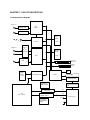
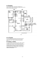
1. System configuration
CHAPTER2. OPTIONS
2. Options
No.
NAME
MODEL
DESCRIPTION
1
ON-LINESYSTEM
ER-A7RS
2 port RS232 I/F
MCR I/F
2
EXPANSION
MEMORYBOARD
ER-03MB
1MBPS-RAM
ER-04MB
2MBPS-RAM
3
REMOTEPRINTER
ER-03RP
4
MCR
(Magnet Card Reader)
ER-A8MR
5
DATA BACK UP
SYSTEM
ER-02FD
ER-04RP
CE-IR2
CE-IR4
FD unit
Wireless I/F for IR
comunication
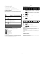
3. Service tools
No.
NAME
PARTSCODE
PRICE
RANK
DESCRIPTION
1
TERMINATOR (50 Ω)
QCNCM7145RCZZ
AZ
2
EXPANSIONPWB
CKOG-6724BHZZ
BX
3
MCR test card
UKOG-6718RCZZ
BE
ForER-A8MR
4
RS232 LOOP BACK CONNECTOR
UKOG-6705RCZZ
BC
For RS232 connector
For SRN in-line system
4. Supplies
No.
NAME
PARTSCODE
PRICE
RANK
1
STANDARDKEYSHEET
PSHEK6849BHZZ
AS
2
PROGRAMMINGKEYSHEET
PSHEK6850BHZZ
AH
3
BLANK KEY SHEET
PSHEK6818BHZZ
AQ
2–2
DESCRIPTION
•
5. How to use service tools
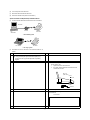
5-1. Expansion PWB : CKOG-6724BHZZ
• Extrenal view
•
Connection diagram
ER-A7RS
ER-A750 bus connector
Plain view
5-2. MCR test card: UKOG-6718RCZZ
Test pins : Used to check the bus signals.
•
•
Bus connector : Used to check the bus signals.
Connected to the ER-A750 Mother PWB.
2–3
Used when executing the diagnostics of the ER-A8MR.
External view
CHAPTER 3. SERVICE PRECAUTION
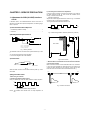
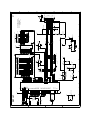
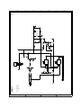
b) Connecting the oscillator and its adjustment
Connect a dummy network or branch-trunk network to the output of
the SRN connector (CON 15), and connect the oscillator to the
dummy or branch-trunk network.
1. Adjustment for SRN (IN-LINE) interface
circuit
* Waveform adjustment
Adjust VR4 until the signal waveform as shown in Fig. 5 is obtained
across IC34 (pin 1 of the 75115) and GND pin.
Turning VR4 clockwise extends the interval of T1.
If transistor Q10 in the transmitter/receiver section has been replaced or if the SRN level requires readjustment, the following alignment is required:
VOH
VOL
T1
1) Tools and Instruments Required
T2
T1 = 580 to 620ms
T2 = 380 to 420ms
1 Oscilloscope (50MHz or better) . . . . . . . . . . . . . . . . . . . . . . . . . . . 1
2 ER-A750 . . . . . . . . . . . . . . . . . . . . . . . . . . . . . . . . . . . . . . . . . . . . 1
Fig. 5 Receiver regeneration waveform (with dummy network)
R2
CON15
VR4
IC34 Q10
2) Dummy Network Specifications
Pin No.1
R1
C1
Main PWB
A
R1 100 Ω J (1/4W carbon)
R2 150 Ω J (1/4W carbon)
C1 0.01µ F (mylar firm)
Fig. 1 Dummy network
⊕
and
R4
The oscillator should be connected to the points indicated by
$.
⊕ : Connect the positive side of the oscillator.
$: Connect the negative side of the oscillator.
3) Connections
Fig. 6 Board location
2 When the Branch Trunk Network and Two POS’S are Available.
Main PWB
a) Connecting terminals
Both ends of the network must be terminated with a 50Ω terminator.
If only two active terminals are tested and left on the network, disconnect all other terminals from the network. (In this case as well,
both ends of the trunk network must be terminated with 50Ω).
BNC connector
Fig. 2
Attach the BNC connector to the SRN connector (CON 15) on the
main PWB.
R50 Ω
R50 Ω
4) Alignment Procedure
1 When Using an Oscillator
a) Checking the 1MHz oscillator output
Using an oscilloscope check the 1MHz oscillator’s output waveform.
5V
ER-A750
ER-A750
0V
0.5µ S
Fig. 7 Terminal connection
0.5µ S
Fig. 3 1MHz oscillator output waveform
NOTE: The oscillator used should have an output impedance of
50Ω.
3–1
b) Receive level adjustment
i) Turn on both the receiver terminal and the transmitter terminal.
2. Battery label
ii) Run the diagnostic program "Flag send check" on the transmitter
terminal to send a flag.
The battery label is attached to the main chassis on the back surface
of the set.
The battery label has the column to show the battery replacement
date. Put down the date in the following cases:
(The battery life is about 3 years after replacement.)
iii) Checking transmitter terminals’ output waveform
Using an oscilloscope, check the transmitter terminal’s output
signal waveform.
1µ S
•
•
When the set is installed.
When the battery is replaced after installation.
CAUTION:
1µ S
When the time written below comes, ask your dealer for a
replacement of the battery.
Fig. 8 Transmitter terminal’s output waveform
(at transmitter output)
VORSICHT:
At the receiver terminal, the transmitter terminal’s output waveform is subject to attenuation and distortion due to the length of
the trunk cable (this depends on the characteristics of the cable
itself).
Wenn die untenbenannte Zeit erreicht wird, ersuchen Sie bitte
Ihren Fachhändler um den Austausch der Batterie.
PRECAUTION:
Lorsque le temps écrit ci-après arrive, demander à votre
revendeur local de remplacer la batterie par une nouvelle.
3.8V
ADVERTENCIA:
0.8V
Cuando se alcance el tiempo indicado abajo, solicite a su
distribuidor que reemplace la batería.
Fig. 9 Example of distorted signal waveform at the receiver terminal
(RG58/U 400m)
Time to replace : ______________________
Austauschzeit : ______________________
Le temps de la remplacer :
______________________
Tiempo de reemplazo :
Adjust the receiver terminal adjust VR4 (20kΩ) on the main PWB
until the waveform as shown in Fig. 10 is obtained at IC34 (pin 1
of the 75115). (For the location of VR4, see Fig. 6 Board location
of this subsection).
Clockwise rotation of VR4 extends the High level pulse width of
the signal at IC34 (pin 1 of the 75115).
3. Precautions in installing optional RAM
PWBs
1µ S
1µ S
1) Background
Fig. 10 Waveform at IC34 (pin 1 of the 75115 IC in the receiver
terminal)
The ER-A750 can use the ER-03MB or the ER-04MB as an optional
RAM PWB. The ER-03MB and the ER-04MB are available in two
versions according to the difference in access time of the pseudoSRAM.
5) Other Checks (These Checks should be done
After the Receive Level Adjustment is
Completed).
1 Line driver bias control circuit
Make sure that the voltage at the A-side lead of the R4 resistor
(150Ω, 3W) shown in Fig. 6 is properly switched.
Procedure:
i) Connect a terminating resistor or read network to the BNC connector, QCNW-6856RCZZ (Fig. 2).
ii) Run the diagnostic program "Data send check", and make sure
that the voltage at point A (in Fig. 6) is switched as shown in Fig.
11.
12V
0V
4.3ms
17ms
Fig. 11 bias circuit switching waveform
iii) If the waveform as shown in Fig. 11 is not obtained, it is most
probable that transistor Q10 (2SC4699) is defective.
2 For the other check items, refer to DIAGNOSTICS
SPECIFICATIONS
3–2
(1)
150 ns access time version (Not marked with "| "; manufactured
before June, 1996; shipped only to North America and Europe)
(2)
120 ns access time version (Marked with "| "); manufactured
after July, 1996 These two versions can be identified, one from
the other, by whether or not the "| " mark is stamped on the
white background as shown in Fig. 1 and by the marking on the
case. (See Fig. 1.)
PWB marking
2) Cautions to be exercised when using the RAM
PWBs with the ER-A750
(ER-03MB/04MB PWB Face side)
When using the above-mentioned RAM PWB version (1) with the
ER-A750, it is necessary to correct the RAM access timing. Use of
the above-mentioned RAM PWB version (2) does not require the
correction of the RAM access timing. For this purpose, a hardware
jumper (JP1), designed to judge to determine whether or not to
correct the RAM access timing, is located on the main PWB of the
ER-A750 (Fig. 2). Before installing an optional RAM PWB, check its
version by referring to the description given in the above-mentioned
(1) and (2) and set the jumper as shown below. (The ER-A750 has
been factory-set for 150ns access time and TP cycle inserted.)
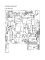
MAIN PWB
Imprint " " on this white area.
Packing case
ZD4
3 2 1
Indivi dual case
IC27
3
1
JP1
E C B
IN case of (2)
Imprint " " on the right side of the
model rabel.
+C17
CE
Q6
1
IC16
IN case of (1)
Short position
Colleclive case
Fig. 3 Setting of the JP1 on the main PWB of the ER-A750
(1)
Setting when the ER-03MB or the ER-04MB is not marked with
"| "
(Position to which the ER-A750 has been factory-set)
1
CE
(2)
Setting when the ER-03MB or the ER-04MB is marked with "| "
1
Imprint " " under the model label.
3–3
3
3
3) Difference in operation according to the setting
of the jumper
5. IPL (Initial Program Loading) function
Only when the ER-03MB or the ER-04MB is used in the above setting
state (1) will one cycle (i.e., cycle for generating pre-charge time of
the quasi-SRAM: TP cycle) of access be additionally inserted into the
CPU, thereby delaying the CPU speed slightly.
1) Introduction
The application software of the ER-A750 is written in the flash ROM
(IC6: VHILH80S01-1). In the following cases, writing procedure of
the application software into the flash ROM is required:
4) Factory-setting of the ER-A750
The ER-A750 has been factory-set so that the JP1 is in the setting
state (1) (TP cycle inserted). However, if it has neither the ER-03MB
or the ER-04MB installed to it, this is automatically detected by software, so the additional insertion of the TP cycle is not performed.
•
When the flash ROM (IC6: VHILH80S01-1) is replaced with new
one. The service part flash ROM does not include the application
software in it.
•
When IPL writing is required because of change in the application
software.
* The service part of the main PWB unit (CPWBX7510BH01) includes the flash ROM (IC6: VHILH80S01-1) with the application
software written in it, and there is no need for writing the application software when replacing the main PWB unit.
Note:
When installing the ER-03MB or the ER-04MB, check the position
of the jumper by referring to Fig. 3.
Improper setting of the jumper may result in malfunction.
2) IPL procedure
There are two ways of IPL procedures.
4. IR module (PRM-850) soldering
conditions
•
•
IPL from P-ROM via ER-A7RS
IPL from PC via IR (infrared) communication
The detailed descriptions on the above procedures are given below.
3) IPL from P-ROM via ER-A7RS
(1)
Main PWB
Install the master ROM to the IC socket (IC12) on the ER-A7RS.
Master ROM: Part code: VHI27801RAA1A
(2)
IPL switch on the ER-A7RS: Set the IPL SW to ON position.
P-ROM
IPL SW
IC12
OFF
ON
Location No.IC1
Part code: VHIRPM850CB-1
When replacing the IR module (IC1), observe the following conditions.
(3)
Install the ER-A7RS to the ER-A750. (The ER-A750 power should
be turned OFF.)
Solder the IR module with the solder tip temperature at 280 degrees
C within 3 sec.
ER-A750
(SIDE VIEW)
ER-A7RS
(4)
Turn on the power of the ER-A750.
(5)
The following display is shown and the IPL procedure is started.
When the procedure is completed, the message of "Completed." is shown.
LCDDISPLAY
IPL from PROM
C0 C1 C2 C3 C4 C5 C6 C7
C8 C9 CA CB CC CD CE CF
Completed.
3–4
(6)
Turn off the power of the ER-A750.
(7)
Remove the ER-A7RS from the ER-A750.
(8)
Perform the master reset. (Refer to CHAPTER 4.)
4) IPL from PC via IR (infrared) communication
(1)
IR communication between the ER-A750 and PC is as follows:
RS-232C
CE-IR4
PC
without IR
ER-A750
1. PC+CE-IR4 system
PC with IR
ER-A750
2. PC only system
(2)
Procedures on the PC side and on the ER-A750 side are as
follows:
No
1
Procedure on P.C. side
No
Procedure on ER-A750 side
Copy “A7IPL.EXE” and S-type ROM object file
(ex. “A750_0A.ROM) into your Personal Computer (P.C.).
* “A7IPL.EXE” and S-type ROM object file is separately
supplied.
2
Turn OFF the power.
3
Select IPL Receiving Mode.
Set IPL switch “ON”.
1
Open the IR cover of the ER-A750.
2
IPL switch: Set the IPLIR SW to the left side when
viewed from the front.
ER-A750
(SIDE VIEW)
IR unit
IPLIR SW
IPLIR SW
4
Turn ON the power.
5
Starting of IPL Receiving Mode.
ER-A750shows
“IPL from IR”
IPL from IR
6
Connect P.C. and ER-A750 via IR.
3–5
7
Execute “A7IPL.EXE” on P.C.
Operation:
> A7IPL
A750_0A.ROM
(“A750_0A.ROM” is file name of S-type ROM object.)
8
Program data is sent to ER-A750 automatically.
8
Program data is received from P.C. automatically.
IPL from IR
Connected IRDA 115200
C1 C2 C3 C4 C5 C6 C7 C8
C9 CA CB CC CD CE CF
9
“A7IPL.EXE” is completed.
9
P.C. shows
ER-A750shows
“Completed.”
“Completed.”
IPL from IR
Connected IRDA 115200
C1 C2 C3 C4 C5 C6 C7 C8
C9 CA CB CC CD CE CF
Completed.
10
Turn OFF the power.
11
Select Normal Mode.
Set IPL switch “OFF”.
12
Execute “Master reset” on ER-A750.
End
3–6
SRV. reset
CHAPTER 4. SRV RESET (Program
Loop Reset) and
switch to SRV mode
Used to return the machine back to its operation state after a lock up
has occurred.
PROCEDURE
In the ER-A750, the following reset switch (location No.: S2) is used
to switch to the service (SRV) mode and to reset.
1) Turn off the AC switch.
2) Set the reset switch to “OFF” position
3) Turn on the AC switch.
4) Turn to “ON” the reset switch.
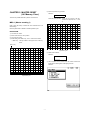
5) The SRV mode is displayed as shown below.
DISPLAY:
Reset
switch
1Side(Rear side):"ON" position(Reset state)
3Side(Front side):"OFF" position(Reset cancel)
4–1
5) Enter the password key operation
CHAPTER 5. MASTER RESET
(All Memory Clear)
DISPLAY:
ENTERPASSWORD
There are two possible methods to perform a master reset.
Password input procedure: Press the four corners of the keyboard in the sequence of a, b, c, and
d.
MRS-1 (Master resetting 1)
c
a
b
d
Used to clear all memory contents and return machine back to its
initial settings.
Return keyboard back to default for default kyeboard layout.
PROCEDURE
1) Turn off the AC switch.
2) Set the reset switch to “OFF” position
3) Turn on the AC switch.
4) While holding down MRS-1 key , turn to “ON” the reset switch.
* MRS-1 key : The key located on Left upper corner of the keyboard.
MRS-1 Key
Keyboard layout
6) Master reset is started.
DISPLAY:
MASTER RESET
7) After completion of the master reset, the buzzer sounds three
times and the following SRV mode display is shown.
DISPLAY:
Keyboard layout
5–1
6) Set the fixed keys in the table below. (Start from the zero “0” key,
The keys are displayed sequentially.)
MRS-2 (Master resetting 2)
Used to clear all memory and keyboard contents. This reset returns
all programming back to defaults.
DISPLAY:
ENTER 0
KEY
The keyboard must be entered by hand. This reset is used if an
application needs different keyboard layout other than that supplied
by a normal MRS-1.
[Key setup procedure]
PROCEDURE
MRS-2
executed
Key
position set
0
Free key
Setup
complete
0
1) Turn off the AC switch.
Disable
2) Set the reset switch to “OFF” position
3) Turn on the AC switch.
NOTES:
4) While holding down MRS-2 key , turn to “ON” the reset switch.
*1: When the 0 key is pressed, the key of the key number on
display is disabled.
* MRS-2 key : The key located on Right upper corner of the
keyboard.
*2: Push the key on the position to be assigned. With this, the
key of the key number on display is assigned to that key
position.
MRS-2 Key
*3: When relocating the keyboard, the PGM 1/2 mode use standard key layout.
Key
Key
Key name
No.
No.
001
Keyboard layout
5) Enter the password key operation
DISPLAY:
“0” key
Key name
Key
No.
Key name
011
“00” key
Decimal point “•”
key
023
“ENTER” key
024
“CA/AT” key
002
“1” key
013
003
“2” key
014
“CL” key
004
“3” key
015
“@/FOR” key
005
“4” key
016
“SBTL” key
006
“5” key
017
“MODE” key
007
“6” key
018
UP “↑ ” key
008
“7” key
019
DOWN “↓ ” key
009
“8” key
020
LEFT “←” key
010
“9” key
021
RIGHT “→” key
022 “CANCEL” key
7) Master reset is started.
ENTERPASSWORD
DISPLAY:
Password input procedure: Press the four corners of the keyboard in the sequence of a, b, c, and
d.
c
MASTER RESET
8) After completion of the master reset, the buzzer sounds three
times and the following SRV mode display is shown.
a
DISPLAY:
b
d
Keyboard layout
5–2
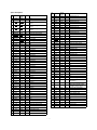
CHAPTER 6. DIAGNOSTICS
SPECIFICATIONS
1. General
CONTENTS
The diagnostics program is built in the standard ROM.
This diagnostics program is used for simplified check of the ER-A750
series operations in servicing.
1. General ..........................................................................................1
2. System configuration .....................................................................1
2-1. Test system.........................................................................1
3. Diagnostics ....................................................................................1
1) Master reset procedure..................................................1
2) Program reset (service reset) procedure .......................1
3-1. Execution of diagnostics .....................................................1
3-2. RAM Diagnostics.................................................................2
1) Standard RAM Check ...................................................2
2) VRAM Check ................................................................2
3) ER-03MB Check ...........................................................3
4) ER-04MB Check ............................................................3
3-3. ROM & SSP Diagnostics.....................................................4
1) Standard ROM Check....................................................4
2) SERVICE ROM Check ..................................................4
3) SSP Check ...................................................................4
3-4. Timer & Keyboard & Clerk Switch Diagnostics ...................5
1) Timer Check .................................................................5
2) Keyboard Check ...........................................................5
3) Clerk SW Check ...........................................................5
3-5. RS232 I/F Diagnostics ........................................................5
1) CHANNEL Check ..........................................................5
2) CH1 Check ....................................................................6
3) CH2 Check ....................................................................6
4) CH3 Check ....................................................................6
5) CH4 Check ....................................................................6
6) CH5 Check ....................................................................6
7) CH6 Check ....................................................................6
8) CH7 Check ....................................................................6
3-6. Liquid Crystal Display Diagnostics ......................................7
1) Liquid Crystal Display Check ........................................7
3-7. Rear Display Diagnostics ....................................................7
1) Rear Display Check ......................................................7
3-8. SHARP Retail Network Diagnostics ....................................8
1) SRN Self Check.............................................................8
2) SRN Flag Send Check...................................................9
3) SRN Data Send Check ..................................................9
4) Data Transmission Check .............................................9
3-9. IrDA & ASK Diagnostics ....................................................10
1) IrDA & ASK Check.......................................................10
2) IrDA & ASK Check (checker mode) .............................10
3) Data Transmission Check (Receive mode) .................10
4) Data Transmission Check (Send mode) ......................11
3-10. Magnetic Card Reader Diagnostics ..................................11
1) Magnetic Card Reader Check ....................................11
3-11. Drawer Diagnostics ...........................................................11
1) Drawer 1 Check ...........................................................11
2) Drawer 2 Check ...........................................................11
2. System configuration
2-1. Test system
ER-A750 only
ER-A750
3. Diagnostics
Starting the diagnostics
This diagnostics program is written in the external ROM and executed
by the CPU (H8/510). To operate this program, the following conditions must be satisfied.
1 The power for the logic system is proper.
(+5V, VRAM, VCKDC, POFF, +24V)
2 The input/output pins and the internal logic of the CPU are normal.
In addition, CKDC7, MPCA7, the system bus, and the standard
ROM/RAM are normal.
To start the machine for the first time, perform the master reset.
In order to add an option unit when the machine is normally operating, perform the program reset.
1) Master reset procedure
1 Turn off the power.
2 Set the CKDC reset switch to RESET position.
3 Turn on the power.
4 While pressing the specified key, set the CKDC reset switch to the
normal position.
2) Program reset (service reset) procedure
1 Turn off the power.
2 Set the CKDC reset switch to RESET position.
3 Turn on the power.
4 Set the CKDC reset switch to the normal position. (Do not press
any key.)
3-1. Execution of diagnostics
To start the diagnostics, select "DIAGNOSTICS" with the cursor in the
menu selection in SRV mode, and press the enter key.
The DIAG MAIN MENU is started and the following menu screen is
display. The cursor position is highlighted. Use ↑ key and ↓ key to
move the cursor. Move the cursor to the process you desire and
press the enter key. The selected individual diagnostics program is
executed. When the individual diagnostics program is completed, the
display returns to the menu screen. To terminate the diagnostics,
press the CANCEL key. Then the display returns to the SRV mode
menu screen.
6–1
ER-A750
Diagnostics
V
2 Display
1.0A
Product§&§Test§Diagnostics
RAM Diagnostics
ROM & SSP Diagnostics
Clock & Keyboard & Clerk
Serial I/O Diagnostics
LCD Diagnostics
Rear Display Diagnostics
SRN Diagnostics
IrDA Diagnostics
MCR Diagnostics
Drawer Diagnostics
Diagnostics End
Standard
RAM Check
Standard
Diagnostics
Error
memory
size
:
512KB
PASS!!(or ERROR!!)
Address
xxxxxxH
Write Data
xxxxH
Read Data
xxxxH
The error address and the bit are displayed only when the error
occurs. (If the error does not occur, they are not displayed.)
3 Terminating procedure
After completion of check, press the CANCEL key.
2) VRAM Check
"Product & Test Diagnostics" is used only in the production
process, and must be not used in servicing.
1 Check content
3-2. RAM Diagnostics
The following check on VRAM is executed. The memory contents
will not be changed by the check.
This diagnostics is used to test the standard RAM and the expansion
RAM.
The following processes are performed for the check address
(100000H ∼ 107FFFH).
The following menu is displayed. The cursor position is highlighted.
Use ↑ key and ↓ key to move the cursor. Move the cursor to the
process you desire and press the enter key. The selected individual
diagnostics program is executed.
PASS1: Memory data save
PASS2: Data "0000H" write
PASS3: Data "0000H" read/compare, data "5555H" write
PASS4: Data "5555H" read/compare, data "AAAAH" write
RAM
Diagnostics
PASS5: Data "AAAAH" read/compare
Standard§RAM§Check
VRAM Check
ER-03MB Check
ER-04MB Check
PASS6: Memory data writed the saved data
In case of a compare error in the check sequences of PASS1 ∼
PASS6, an error display is made. If there is no error at all, the
check is normally terminated.
In addition, the following address check is performed in the above
check sequence.
1) Standard RAM Check
1 Check content
In case of an error, an error display is made and read/write of the
address where the error occurred is repeated.
For the pseudo SRAM of the standard RAM 512KB, the following
check is performed. The memory contents will not be changed by
this check.
Check point address = 100000H, 100001H
100002H, 100004H
100008H, 100010H
100020H, 100040H
100080H, 100100H
100200H, 100400H
100800H, 101000H
102000H
The following processes are performed for the memory address
(180000H ∼ 1FFFFFH) to be checked.
PASS1: Memory data save
PASS2: Data "0000H" write
PASS3: Data "0000H" read/compare, data "5555H" write
PASS4: Data "5555H" read/compare, data "AAAAH" write
2 Display
PASS5: Data "AAAAH" read/compare
VRAM
PASS6: Memory data writed the saved data
In case of a compare error in the check sequences of PASS1 ∼
PASS6, an error display is made. If there is no error at all, the
check is normally terminated.
Check
VRAM memory
RROR!!)
Error
In addition, the following address check is performed.
In case of an error, an error display is made and read/write of the
address where the error occurred is repeated.
size
:
32KB
PASS!!(or
E
Address
xxxxxxH
Write Data
xxxxH
Read Data
xxxxH
The error address and the bit are displayed only when the error
occurs. (If the error does not occur, they are not displayed.)
Check point address = 180000H, 180001H
180002H, 180004H
180008H, 180010H
180020H, 180040H
180080H, 180100H
180200H, 180400H
180800H, 181000H
188000H, 190000H
1A0000H, 1C0000H
3 Terminating procedure
After completion of check, press the CANCEL key.
6–2
3) ER-03MB Check
4) ER-04MB Check
1 Check content
1 Check content
The ER-03MB presence check is performed in the following procedure. The memory contents will not be changed by this check.
The ER-04MB presence check is performed in the following procedure. The memory contents must not be changed by this check.
•
•
55AAH is written into 2FFFFEH.
•
•
55AAH is written into 3FFFFEH.
55AAH is written into 3FFFFEH.
•
•
55AAH is written into 2FFFFEH.
•
•
2FFFFEH is read and compared with 55AAH. If the both data
are correct, the following procedure is performed. If not, "Extended RAM size: 0KB" is displayed and the check is terminated.
3FFFFEH is read and compared with 55AAH. If the both data
are not correct, the following procedure is performed. If correct,
"Extend RAM is : ER-04MB" is displayed and the check is
terminated.
3FFFFEH is read and compared with 55AAH. If the both data
are correct, the following procedure is performed. If not, go to
????????.
2FFFFEH is read and compared with 55AAH. If the both data
are correct, "Extend RAM is : ER-03MB" is displayed and the
check is terminated. If not, "Extended RAM size : 0KB" is displayed and the check is terminated.
For the ER-04MB, the following check is performed.
For the ER-03MB, the following check is performed.
The following processes are performed for the check address
(200000H ∼ 3FFFFFH).
The following processes are performed for the check address
(200000H ∼ 2FFFFFH).
PASS1: Memory data save
PASS1: Memory data save
PASS2: Data "0000H" write
PASS2: Data "0000H" write
PASS3: Data "0000H" read/compare, data "5555H" write
PASS3: Data "0000H" read/compare, data "5555H" write
PASS4: Data "5555H" read/compare, data "AAAAH" write
PASS4: Data "5555H" read/compare, data "AAAAH" write
PASS5: Data "AAAAH" read/compare
PASS5: Data "AAAAH" read/compare
PASS6: Memory data writed the saved data
PASS6: Memory data writed the saved data
In case of a compare error in the check sequences of PASS1 ∼
PASS6, an error display is made. If there is no error at all, the
check is normally terminated.
In case of a compare error in the check sequences of PASS1 ∼
PASS6, an error display is made. If there is no error at all, the
check is normally terminated.
In addition, the following address check is performed in the above
check sequence.
In addition, the following address check is performed in the above
check sequence.
In case of an error, an error display is made and read/write of the
address where the error occurred is repeated.
In case of an error, an error display is made and read/write of the
address where the error occurred is repeated without performing
the check.
Check point address = 200000H, 200001H
200002H, 200004H
200008H, 200010H
200020H, 200040H
200080H, 200100H
200200H, 200400H
200800H, 201000H
202000H, 204000H
208000H, 210000H
220000H, 240000H
280000H
Check point address = 200000H, 200001H
200002H, 200004H
200008H, 200010H
200020H, 200040H
200080H, 200100H
200200H, 200400H
200800H, 201000H
202000H, 204000H
208000H, 210000H
220000H, 240000H
280000H, 300000H
2 Display
ER-03MB
2 Display
Check
Extended
ER-04MB
RAM
size
:
1024KB
PASS!!(or
ERR
Check
Extended
OR!!)
RAM
size
:
2048KB
PASS!!(or
ERR
OR!!)
Error
Address
xxxxxxH
Write Data
xxxxH
Read Data
xxxxH
Error
The error address and the bit are displayed only when the error
occurs. (If the error does not occur, they are not displayed.)
Address
xxxxxxH
Write Data
xxxxH
Read Data
xxxxH
The error address and the bit are displayed only when the error
occurs. (If the error does not occur, they are not displayed.)
3 Terminating procedure
3 Terminating procedure
After completion of check, press the CANCEL key.
After completion of check, press the CANCEL key.
6–3
3-3. ROM & SSP Diagnostics
2) SERVICE ROM Check
The standard ROM and the service ROM are checked. The SSP
circuit is also checked.
1 Check content
The standard ROM area (D00000H ∼ DFFFFFH) is added in the
unit of byte. If the lower two digits of the result is 10H, it is normal.
The ROM version and the model name code which are stored in
address DFFFE0H ∼ DFFFEFH where the ROM version and the
check sum correction data are stored are displayed. The format of
data (ASCII) to be stored is as follows:
The following menu is displayed. The cursor position is highlighted.
Use ↑ key and ↓ key to move the cursor. Move the cursor to the
process you desire and press the enter key. The selected individual
diagnostics program is executed.
ROM
& SSP
DFFFE0H ∼ DFFFEFH: Model name code (example: ER-A750.
Display is made up to 00H of data.)
Check
Standard§ROM§Check
Service ROM Check
SSP Check
DFFFF0H ∼ DFFFF9H: 27801R****(****=PROGRAM VERSION)
DFFFFAH ∼ DFFFFBH: BLOCK NO. ("CO" ∼ "CF")
DFFFFCH: TERMINATOR ("=")
1) Standard ROM Check
DFFFFDH ∼ DFFFFEH: BLOCK VERSION (example "00")
1 Check contents
DFFFFFH: CHECK SUM CORRECTION DATA
The standard ROM area (C00000H ∼ CFFFFFH) is added in the
unit of byte. If the lower two digits of the result is 10H, it is normal.
The ROM version and the model name code which are stored in
address CFFFE0H ∼ CFFFEFH where the ROM version and the
check sum correction data are stored are displayed. The format of
data (ASCII) to be stored is as follows:
This SERVICE ROM allows to write into the FLASH ROM when
re-execution is impossible because of an abnormality during
rewriting into the FLASH ROM. The composition is the same as
the standard ROM.
The program version of the IPL is displayed so that 0PAGE where
the IPL is stored is individually controlled.
CFFFE0H ∼ CFFFEFH: Model name code (example: ER-A750.
Display is made up to 00H of data.)
2 Display
CFFFF0H ∼ CFFFF9H: 27801R****(****=PROGRAM VERSION)
Service ROM Sum Check
IPL PROGRAM Version
CFFFFAH ∼ CFFFFBH: BLOCK NO. ("CO" ∼ "CF")
CFFFFCH: TERMINATOR ("=")
:
**
CFFFFDH ∼ CFFFFEH: BLOCK VERSION (example "00")
APL
CFFFFFH: CHECK SUM CORRECTION DATA
A750
BLOCK Version
The flash ROM used as the standard ROM has rewriting block of
64KB as the unit. To control the version in each block, the composition is the same as the above CFFFF0H or later and arranged
in each 64KByte. At that time, correction is made so that the sum
of each block becomes 01H, and the total of 1MByte is 10H.
PROGRAM
Version
27801R****
PASS!!(or
ERROR!!)
← Displays the version.
ER
C0=**,C1=**,C2=**,C3=**
C4=**,C5=**,C6=**,C7=**
:
3 Terminating procedure
The program version of the IPL is displayed so that 0PAGE where
the IPL is stored is individually controlled.
After displaying the check result, press the CANCEL key to terminate the check.
2 Display
3) SSP Check
Standard ROM Sum Check
IPL PROGRAM Version
:
PASS!!(or
**
APL
PROGRAM
Version
27801R****
1 Check content
ERROR!!)
By starting this check program, the SSP setting for checking is
automatically performed and the SSP check is executed and the
result is displayed.
← Displays the version.
ER
The SSP check sets data for check in the vacant space in the
SSP entry register, and deletes the data for check after completion of checking. Therefore, the already set data are not changed
by this check.
A750
BLOCK Version
C0=**,C1=**,C2=**,C3=**
C4=**,C5=**,C6=**,C7=**
:
2 Display
3 Terminating procedure
SSP
After displaying the check result, press the CANCEL key to terminate the check.
Check
SSP (NMI)
Check
:
PASS!!(ERROR!
!)
3 Terminating procedure
After displaying the check result, press the CANCEL key to terminate the check.
6–4
The following menu is displayed. The cursor position is highlighted.
Use ↑ key and ↓ key to move the cursor. Move the cursor to the
process you desire and press the enter key. The selected individual
diagnostics program is executed. When the CANCEL key is pressed,
the display returns to the diagnostics menu.
3-4. Timer & Keyboard & Clerk Switch Diagnostics
The operation of the clock crystal of CKDC, the keyboard, and the
clerk switch are tested.
When the CANCEL key is pressed, the display returns to the diagnostics menu.
When setting channels of RS232, do not set two or more ports to
one channel. In the ER-A750, max. two units of ER-A7RS can be
installed. In each PWB, do not set two or more ports to the same
channel. If two or more ports should be set to one channel, the
hardware would be destroyed.
Timer & Keyboard & Clerk SW Diagnostics
DATA & TIME = YY/MM/DD & HH:MM
KEY CODE = ***
in the display is highlighted every 500ms.
CLERK CODE = ***
RS232
I/F
Diagnostics
CHANNEL§Check
CH1 Check
CH2 Check
CH3 Check
CH4 Check
CH5 Check
CH6 Check
CH7 Check
1) CHANNEL Check
1 Check content
The CHANNEL setting of the connected RS232 is displayed. The
display content and the setting of DIP SW for CHANNEL setting
on the RS232 I/F PWB are compared.
1) Timer Check
1 Check content
Since the RS232 on the main PWB of the ER-A750 is fixed to
CH1 and CH2, that in the ER-A7RS must be set to CH3 ∼ CH7.
The operation of the clock crystal of CKDC7 is checked.
"YY/MM/DD & MM:HH" in the display is highlighted every 500ms.
Check the highlighted display.
RS232
2) Keyboard Check
I/F
Diagnostics
CHANNEL
1 Check content
← Display when channel present
Check
The A750 main body keyboard input test is performed. The position code corresponding to the inputted key is displayed in three
digits. The key layout corresponding to the input is displayed on
the LCD screen. Press the corresponding key to input. The display
of the inputted key is changed from white square k to black square
Ç and a catch sound is generated.
CH1
=
exis
CH2
=
exis
CH3
=
no
CH4
=
no
CH5
=
no
CH6
=
no
CH7
=
no
← Display when no channel
t!
t!
ne!
3) Clerk SW Check
ne!
1 Check content
ne!
The code of the key which is inserted into the clerk key switch is
displayed in a hexadecimal number.
ne!
3-5. RS232 I/F Diagnostics
ne!
The main PWB and the option PWB (RS232 interface of ER-A7RS)
are checked. Attach the 9-pin D-Sub loop back connector (UKOG6717RCZZ) of wiring in Fig. 3-11.
(Reference) ER-A7RS CHANNEL setting (In the table below, "1" =
SW OFF, "0" = SW ON.)
ER-A7RS CON2
CD
1pin
RD
2pin
SD
ER
S1-1
S1-2
S1-3
0
0
0
Invalid
3pin
0
0
1
CHANNEL 1: Impossible to set
4pin
0
1
0
CHANNEL 2: Impossible to set
GND
5pin
0
1
1
CHANNEL 3
DR
6pin
1
0
0
CHANNEL 4
1
0
1
CHANNEL 5
1
1
0
CHANNEL 6
1
1
1
CHANNEL 7
RS
7pin
CS
8pin
CI
9pin
Fig. 3-11. Wiring diagram of loop back connector (UKOG-6717RCZZ)
6–5
CHANNEL
2 Display
ER-A7RS CON3
S1-4
S1-5
S1-6
0
0
0
Invalid
CHANNEL
0
0
1
CHANNEL 1: Impossible to set
0
1
0
CHANNEL 2: Impossible to set
0
1
1
CHANNEL 3
1
0
0
CHANNEL 4
1
0
1
CHANNEL 5
ERROR
No.
1
1
0
CHANNEL 6
1
ER-DR:ERROR
ER-DR LOOP ERROR
1
1
1
CHANNEL 7
2
ER-CI:ERROR
ER-CI LOOP ERROR
3
RS-CD:ERROR
RS-CD LOOP ERROR
4
RS-CS:ERROR
RS-CS LOOP ERROR
5
CI INT:ERROR
CI interruption is not made.
6
CD INT:ERROR
CD interruption is not made.
7
CS INT:ERROR
CS interruption is not made.
8
TXEMP:ERROR
TXEMP is not set.
RS232
2) CH1 Check
1 Check content
When the channel is not set, an error display is made
(ERROR:CH1). When the channel is set, the following check is
performed.
Control signal check
ERROR!!
ERROR display
ERROR content
9
TXEMP INT:ERROR
TXEMP interruption is not made.
10
TXRDY:ERROR
TXRDY interruption is not made.
11
TXRDY INT:ERROR
TXRDY interruption is not made.
12
RCVRDY:ERROR
RCVRDY is not set.
(Reception enabled. TR-Q is
generated during check)
ERn
RSn
DRn
CIn
CDn
CSn
OFF
OFF
OFF
OFF
OFF
OFF
OFF
ON
OFF
OFF
ON
ON
ON
OFF
ON
ON
OFF
OFF
13
RCVRDY INT:ERROR RCVRDY interruption is not made.
ON
ON
ON
ON
ON
ON
14
SD-RD:ERROR
SD-RD LOOP ERROR
(DATA ERROR)
15
SD-RD:ERROR
SD-RD LOOP ERROR (DATA
ERROR, FRAMING ERROR, etc.)
16
TIMER:ERROR
TIMER ERROR (TMRQ is not set
after completion of check.)
17
TIMER INT:ERROR
TRQ-1 interruption is not made.
The read check of the above inputs and the interruption check
of CS, CI, and CD are performed.
In the read check, ER and RS are changed over in the above
sequence and the logic states of DR, CI, CD, and CS are
checked.
If the logic differs from that in the table, an error display is
made.
3 Terminating procedure
"ON" in the table means Active LOW, and "OFF" means Active
HIGH.
3) CH2 Check
Press the CANCEL key to terminate the check.
In the interruption check, an interruption of CS, CI, or CD is
allowed one by one. (MASK is canceled.)
1 Check content
The check procedure, the display, and the terminating procedure
are the same as CH1 Check.
If an interruption is not made when each signal is active, or if
an interruption is made when each signal is not active, an error
display is made.
4) CH3 Check
1 Check content
The above check is repeated four cycles.
The check procedure, the display, and the terminating procedure
are the same as CH1 Check.
Data transfer check
The loop back data (256 bytes) of 00H ∼ 0FFH are used for
data transfer check. The baud rate is set to 38400BPS.
•
:
All the contents of an error must be displayed.
Press the CANCEL key to terminate the check.
•
Check
ER-DR
2 Terminating procedure
•
CH1
5) CH4 Check
1 Check content
Timer check (RS232 on board timer)
The check procedure, the display, and the terminating procedure
are the same as CH1 Check.
Before performing the check, set the timer to TCVDT start and
5ms. Then perform the following procedure.
* During execution of the
generated.
6) CH5 Check
check, TRQ- must not be
1 Check content
The check procedure, the display, and the terminating procedure
are the same as CH1 Check.
* After 5ms from completion of the check, TRQ- must be
generated.
7) CH6 Check
1 Check content
The check procedure, the display, and the terminating procedure
are the same as CH1 Check.
8) CH7 Check
1 Check content
The check procedure, the display, and the terminating procedure
are the same as CH1 Check.
6–6
3-6. Liquid Crystal Display Diagnostics
•
Reversed pattern of the above
•
The outermost peripheral of the LCD’s active area is displayed
in one-dot line.
•
"H" pattern. "H" is displayed in 40 digits and 15 lines. The 15th
line only has 39 digits of "H."
The ER-A750 LCD display is checked.
The test program displays the patterns in the following sequence.
Every time when the ENTER key is pressed, the next pattern is
displayed. When the ENTER key is pressed at the final pattern, or
when the CANCEL key is pressed at the midst of the check, the
display returns to the menu screen.
1) Liquid Crystal Display Check
1 Check content
The test patterns are displayed in the following sequence. When
the ENTER key is pressed, the next pattern is displayed.
•
Black and white pattern at 1 dot pitch
•
Reversed pattern of the above
•
Vertical stripe pattern at 1 dot pitch
3 Terminating procedure
Press the ENTER key at the final pattern, or press the CANCEL
key to terminate the check.
3-7. Rear Display Diagnostics
The rear display is checked.
•
Reversed pattern of the above
The test program displays the following patterns. When the CANCEL
key is pressed, the display returns to the diagnostics menu.
1) Rear Display Check
1 Check content
The test patterns are displayed in the following sequence. When
the ENTER key is pressed, the next pattern is displayed.
•
•
The test pattern below is displayed.
•
The test pattern with all the elements ON is displayed.
Horizontal stripe pattern at 1 dot pitch
6–7
•
2 Display
Rear
Display
Check
Execute diagnostics command 5. The error status is displayed.
The names and the directions of the signals which are subject
to diagnostics 5 command are as shown in the table below.
Signal name
Power interruption notice
Host → Controller
Power interruption ON initialization
Host → Controller
3 Terminating procedure
Press the CANCEL key to turn off all the elements of the rear
display.
Direction
Power interruption ON continuation
Host → Controller
Power interruption process complete
Host ← Controller
3-8. SHARP Retail Network Diagnostics
CH1 reception data present.
Host ← Controller
The SRN test is performed.
CH2 reception data present.
Host ← Controller
To perform this test, the following composition is required.
•
•
•
Check that the target bit of two statuses obtained by diagnostics 5 command is "0" for ST1 and "1" for ST2. (The other bits
must be masked.) In the other cases, the error status is displayed with the error occurrence bit as "1." The normal bit
shows "0."
ER-A750
Terminal resistor
Branch (trunk) cable (only for data transfer test)
The error status from the host to the controller is as shown in
the table below.
The following menu is displayed. The cursor position is highlighted.
Use ↑ key and ↓ key to move the cursor. Move the cursor to the
process you desire and press the enter key. The selected individual
diagnostics program is executed. When the individual diagnostics
program is completed, the display returns to this menu screen. When
the CANCEL key is pressed, the display returns to the diagnostics
menu.
SRN
b7 Not used. ("0" is always displayed.)
b6 Power interruption notice
b5 Not used. ("0" is always displayed.)
b4 Not used. ("0" is always displayed.)
b3 Not used. ("0" is always displayed.)
Diagnostics
b2 Not used. ("0" is always displayed.)
b1 Power ON continuation
Self§Check
Flag Send Check
Data Send Check
Data Check (Satellite Machine)
Data Check (Master Machine)
b0 Power ON initializing
The error status from the controller to the host is as shown in
the table below.
b7 Not used. ("0" is always displayed.)
1) SRN Self Check
b6 Power interruption notice
1 Check content
b5 Not used. ("0" is always displayed.)
The ROM and RAM for SRN are checked, and CTC interruption
and carrier sense are checked. Also ADLC function and transmission/reception DMA check is made by using the self loop function
of ADLC (MC6854). In addition, the other signals are checked.
The check procedure is as follows:
•
Execute diagnostics command 2. The number of resending is
displayed.
•
Execute diagnostics command 0. The error status is displayed.
The error status is as shown in the table below. When an error
occurs in this test, the following tests are not performed.
b7
b6
b5
b4
b3
b2
b1
b0
•
b4 CH2 reception data exits.
b3 CH1 reception data exits.
b2 Power interruption process complete
b1 Not used. ("0" is always displayed.)
b0 Not used. ("0" is always displayed.)
2 Display
SRN
An error occurs. (The error print is always 1.)
An unexpected interruption is made.
A collision is generated.
An interruption of send complete cannot be made.
(DMAC TC UP interruption)
An interruption of carrier OFF cannot be made. The
mirror image of carrier OFF shows carrier ON.
An interruption of CTC CH2 or CH3 cannot be made.
(Timer interruption)
ROM sum check error
TAM error
CNT.=xxx The number of resending is displayed
in xxx with a decimal number.
ACK
RETRY
CNT.=x In the sequence of b7, b6, ..., b0 from
the left. "1" is displayed in case of an
xx
→:xxxx error, and "0" when normal.
DIAG 0
xxxx—
DIAG 1
xxxx—
_DIAG 5
H→C
xx—
Execute diagnostics command 1. The error status is displayed.
The error status is as shown in the table below.
b7
b6
b5
b4
b3
b2
b1
b0
Self Check
DATA RETRY
An error is generated. (The error print is always 1.)
An unexpected interruption is generated.
DMA sent data and received data are different.
The number of data received in DMA is abnormal.
The number of data transmitted in DMA is abnormal.
An overrun error is generated.
An underrun error is generated.
An interruption of send complete cannot be made.
(DMAC TC UP interruption)
DIAG 5
H←C
In the sequence of b7, b6, ..., b0 from
the left. "1" is displayed in case of an
error, and "0" when normal.
→:xxxx In the sequence of b7, b6, ..., b0 from
the left. "1" is displayed in case of an
error, and "0" when normal.
In the sequence of b7, b6, ..., b0 from
:xxxxxx the left. "1" is displayed in case of an
error, and "0" when normal.
:xxxxx
xxx—
3 Terminating procedure
Press the CANCEL key to terminate the check. After terminating,
perform the service reset.
6–8
•
2) SRN Flag Send Check
1 Check content
In the menu screen, select "Data Transmission Check (Master
Machine)." The display is as shown below.
Execute diagnostics 3 command to send Flag (7EH) continuously.
2 Display
SRN
Flag
Data
Send
Check
Perform the service reset.
3) SRN Data Send Check
Data
1 Check content
Execute diagnostics 4 command to send data of 00H ∼ FFH
(256Byte) as one packet at 12.8msec packet interval at 1Mbps
continuously.
Send
Check
Input
Terminal
Master
(Master)
Number
:
Transmission
Check
(Master)
Input
Master
Terminal
Input
Satellite
: – The entered
Number
terminal No. is
displayed.
xxx
2 Display
Data
Transmission
Enter the terminal No. (000 ∼ 254, 3 digits) of the machine to
be checked and press the ENTER key. The display is as shown
below.
3 Terminating procedure
SRN
Master machine setting
Terminal
Number:
Enter the terminal No. (000 ∼ 254, 3 digits) of the machine to
be connected to the machine to be checked and press the
ENTER key. The display is as shown below.
Check
3 Terminating procedure
Data
Transmission
Check
(Master)
Perform the service reset.
Input
Input
4) Data Transmission Check
Data transmission is checked in an actually composed system. The
system is composed of one master machine and max. 15 satellite
machines.
terminal No. of
satellite machine
is displayed.
Note for starting the check
•
When checking the set in which the SRN setting has been made,
cancel the SRN setting before starting this check.
•
When checking the actually composed system, disconnect the
SRM cables of the sets which are not checked, or cancel the SRN
setting. If it is set to "SRN exits," data may be destroyed.
•
The transmission check setting must be performed after canceling
the SRN setting of all the sets in the system. First, set the satellite
machines, then set the master machine.
When checking with two or more satellite machines connected,
enter the terminal No. (000 ∼ 254, 3 digits) and press the
ENTER key similarly. To execute, press the ENTER key
without entering the terminal No. The display is as shown
below. Do not use the same terminal No. for different machines
(master/satellite).
Data
Transmission
Check
(Master)
Input Master Terminal Number
Input Satellite Terminal Number : xxx
xxx xxx xxx xxx xxx
1 Setting procedure
•
Master Terminal Number
:xxx
– The entered
Satellite Terminal Number:xxx
Satellite machine setting
In the menu screen, select "Data Transmission Check (Satellite)."
Data
Sequence
:
xxx
Number
:
0000
The display is as follows:
Data
Transmission
Check
With the above setting, data transmission between the master
machine and the satellite machine is started.
(Satellite)
2 Check content
Input
Terminal
Number
:
•
Enter the terminal No. (000 ∼ 254, 3 digits) of the machine to
be checked and press the ENTER key. The display is as shown
below.
Data
Transmission
Check
(Satellite)
Input Terminal Number :
Data Sequence Number
xxx
:
– The entered terminal
Data in the following format composed of 2byte sequence No.
and 254byte AAH data are transmitted from the master
machine to the satellite machine. The master machine displays
the sequence No.
1
2
3
4
5
XX
XX
AA
AA
AA
254 255 256 Byte
AA
AA
AA
XXXX : Sequence No. (2byte: 4digits of binary decimal numbers)
AA
: Transmission data (AAH) x 254 bytes
No. is displayed.
0000
6–9
•
The satellite machine sends back the received data to the
master machine. The satellite machine displays the received
sequence No.
•
The master machine receives the data, and checks the sequence No. and 256byte AAH data. In case of an error, the
master machine displays an error code and terminates the
check. If two or more satellite machines are used, the above
operation is repeated. If data transmission with all the satellite
machines are normally completed, the master machine increments the sequence No.
The above operation is repeated.
1) IrDA & ASK Check
IR communication is checked between the ER-A750 sending unit and
the receiving unit.
3 Error display
Data
Transmission
Input
Check
(Master)
Master Terminal
Number
1 Check content
:
•
Data transmission is made from the machine to be checked in
ASK format. The transmission rate is 9600bps. Data of 00H,
11H, 22H, 33H, 44H, 55H, 66H, 77H, 88H, 99H, AAH, BBH,
CCH, EEH, and FFH are transmitted.
•
•
The checker machine sends back the received data.
•
Data transmission is made from the machine to be checked in
IrDA format. The transmission rate is 9600bps. Data of 00H,
11H, 22H, 33H, 44H, 55H, 66H, 77H, 88H, 99H, AAH, BBH,
CCH, EEH, and FFH are transmitted.
•
•
The checker machine sends back the received data.
xxx
Input Satellite Terminal
xxx xxx xxx xxx xxx
Number :
xxx
Data Sequence Number
: xxxx
IRC Error
: xx —
The error
code is
displayed.
The error codes are as shown below.
01 Command abnormality (except for during transmission)
02 No data received.
03 Received data present.
Received data remained.
04 Remote station not ready (in sending)
"NTDY" is sent back because the remote station is not ready
for reception.
The machine to be checked compares the data sent back and
the data transmitted first. If both data are the same, it displays
"PASS !!," and if not the same, "ERROR !!."
2 Display
05 Reception buffer full (in sending)
The controller reception buffer of the remote machine is full.
IrDA & ASK Check
DATA (or TIMEOUT)
:
PASS!!(or
06 Resend error (in sending)
Retry over (5 times) when no response
3 Terminating procedure
07 Collision error (in sending)
When an collision occurred in data transmission, retry over
(16 times) at re-collision after a random time (0 ∼ 255ms).
2) IrDA & ASK Check (checker mode)
ERROR!!)
Press the CANCEL key to terminate the check.
Set the checker machine (ER-A750) corresponding to the above
check content (1).
08 Line busy time out
Transmission cannot be made by multi-station communication
to cause time out in data send wait time.
2 Display
09 Reception size over (in receiving)
The reception buffer size is insufficient.
IrDA & ASK Check (CHECKER MODE)
DATA (or TIMEOUT) :
PASS!!(or ERROR!!)
0A Hardware error
Interface abnormality (No SRN interface or abnormality in
SRN controller)
3 Terminating procedure
Press the CANCEL key to terminate the check.
3 Terminating procedure
3) Data Transmission Check (Receive mode)
Press the CANCEL key to terminate the check. After terminating,
perform the service reset.
1 Check content
Continuous IR communication between the ER-A750 and the ERA750. This mode is on the reception side. When data of 256byte
(00H ∼ 0FFH) are received, data packet counter is incremented by
one. Check that the counter increments.
3-9. IrDA & ASK Diagnostics
This is used to check the IR communication.
To execute this check, the following composition is required.
•
•
The machine to be checked compares the data sent back and
the data transmitted first. If both data are the same, it displays
"PASS !!," and if not the same, "ERROR !!."
2 Display
ER-A750
Data Transmission Check (Receive MODE)
COUNTER : **** (The RING COUNTER (0-9999) is displayed.)
ER-A750 as checker
The following menu is displayed. The cursor position is highlighted.
Use ↑ key and ↓ key to move the cursor. Move the cursor to the
process you desire and press the enter key. The selected individual
diagnostics program is executed. When the CANCEL key is pressed,
the display returns to the diagnostics menu.
IR (IrDA &
ASK)
3 Terminating procedure
Press the CANCEL key to terminate the check.
Diagnostics
IrDA§&§ASK§Check
IrDA & ASK Check (CHECKER MODE)
Data Transmission Check (Receive MODE)
Data Transmission Check (Send MODE)
6 – 10
4) Data Transmission Check (Send mode)
3-11. Drawer Diagnostics
1 Check content
This diagnostics is used to check the drawer open and sensors.
Continuous IR communication between the ER-A750 and the ERA750. This mode is on the transmission side. When data of 256byte
(00H ∼ 0FFH) are transmitted, data packet counter is incremented by
one. Check that the counter increments.
The following menu is displayed. The cursor position is highlighted.
Use ↑ key and ↓ key to move the cursor. Move the cursor to the
process you desire and press the enter key. The selected individual
diagnostics program is executed. When the CANCEL key is pressed,
the display returns to the diagnostics menu.
2 Display
Drawer Diagnostics
Drawer1 Check
Drawer 2 Check
Data Transmission Check (Send MODE)
COUNTER : **** (The RING COUNTER (0-9999) is displayed.)
3 Terminating procedure
1) Drawer 1 Check
Press the CANCEL key to terminate the check.
1 Check content
The solenoid of drawer 1 is turned on, and the drawer open
sensor value is sensed at every 100ms, and the state is displayed.
3-10. Magnetic Card Reader Diagnostics
Read check of the optional ER-A8MR + ER-A7RS is performed.
2 Display
The test program reads the magnetic card of ISO 7811/1-5 standard
and displays the data. When the CANCEL key is pressed, the display
returns to the diagnostics menu.
Drawer 1 Check
Drawer Open
Sensor
:
OPEN
(or CLOSE)
1) Magnetic Card Reader Check
3 Terminating procedure
1 Check content
Press the CANCEL key to terminate the check.
The test program reads tracks 1 and 2 of the magnetic card of
ISO 7811/1-5, and displays the data in ASCII code.
2) Drawer 2 Check
2 Display
MCR
1 Check content
(Magnetic
Card
Reader)
The solenoid of drawer 2 is turned on, and the drawer open
sensor value is sensed at every 100ms, and the state is displayed.
Check
The display and the terminating procedure are the same as
Drawer 1 Check.
TRACK1:
xxxxxxxxxxxxxxxxxxxxxxxxxxxxxxxxxxxxxxxxxxxxxxxxxxxxxxxxxxxx
TRACK2:
xxxxxxxxxxxxxxxxxxxxxxxxxxxxxxxxxxxxxxxxxxxxxxxxxxxxxxxxxxxx
XXXXX shows the data read by the MCR. Incase of an error, the
error code is displayed as shown below.
Magnetic Card
TRACK1:
TRACK1:
TRACK2:
TRACK2:
Reader Check
BUFFER EMPTY
MCR ERROR
BUFFER EMPTY
MCR ERROR
– Displayed when TRACK1 empty code is sent back.
– Displayed when TRACK1 error code is sent back.
– Displayed when TRACK2 empty code is sent back
– Displayed when TRACK2 error code is sent back.
3 Terminating procedure
Press the CANCEL key to terminate the check.
6 – 11
CHAPTER 7. CIRCUIT DESCRIPTION
1. Hardware block diagram
Drawer x 2
DRIVER +24V
CPU
H8/510
DRIVER +24V
FLASH
(ROM)
IR
RS232 x 2
1MB
MPCA7
USART
&
DRIVER/
RECEIVER
PSEUDO
SRAM
512KB
OPC1
EXT.SLOT
(80pin x 2)
SRN
RAMCN
(50pin)
SW
VRAM
(SRAM
32K)
LCD CONTROLLER
CKDC7
KEY
CUSTOMER DISP.
POWER SUPPLY FOR
VACUUM FLUORESCENT
TUBE
BRIGHTNESS
CONTROL KNOB
+24V
INVERTOR
LCD
320 x 240 dots
LIQUID-CRYSTAL BIAS
POWER SUPPLY
+5V
-24V
VCC
CONTRAST
ADJUSTMENT
/KNOB
7–1
POWER SUPPLY
2. Description of main LSI’s
2-1. CPU (HD6415108FX)
7-2
2) Block diagram
P27/A23
P26/A22
Data bus
Port 1
Port 2
P25/A21
P24/A20
P23/A19
P22/A18
P21/A17
X
Clock
oscillator
Watch
dog timer
Address bus
E
Address bus
XTAL
Data bus (Lower)
EXTAL
Data bus (Upper)
P20/A16
MD2
MD1
H8/500 CPU
DTC
MD0
RES
STBY
NMI
Interruption controller
AS
P37
RD
P36
HWR
LWR
A15
A14
A13
A12
A11
A10
A9
A8
A7
A6
A5
A4
A3
A2
A1
A0
P35
Refresh controller
RFSH
16bit free running
timer x 2ch
P34
P33
BREQ
VCC
Wait state
controller
8bit timer
A/D convertor
Serial
communication
interface x 2ch
BACK
WAIT
VCC
P47
VCC
VSS
VSS
P46
P45
VSS
P44
VSS
P43
VSS
P42
VSS
P41/TMCI
VSS
P40
VSS
AVCC
AVSS
Port 8
Port 7
Port 6
Fig. 2-2
7–3
Port 5
3) Pin description
Pin
Symbol
No.
1 RES
Signal
name
RESET
In/
Function
Out
I/O Reset input
Non-maskable interrupt input for
In
SSP interrupt input.
2
NMi
NMi
3
VSS
NU
4
P10
IPLON0
5
P11
6
P12
7
P13
PNLSNS In IPLON signal for servicing
LCD sensing signal at main
IPLON2 In
PWB side
NORDY In Flash memory RY/BY # signal
8
P14
FVPON
In GND
IPLON signal for factory setting
In
(from expansion I/O port)
9 P15
10 P16
BKLT
Nu
Flash memory write protect
signal output
Out Backlight control signal
In GND
11 P17
12 D8
13 D9
MVDT
D0
D1
In Memory version detect
I/O Data bus
I/O Data bus
14 D10
15 D11
16 D12
D2
D3
D4
I/O Data bus
I/O Data bus
I/O Data bus
17 D13
18 D14
19 D15
D5
D6
D7
I/O Data bus
I/O Data bus
I/O Data bus
20 VSS
21 A0
22 A1
NU
A0
A1
In GND
Out Address bus
Out Address bus
23 A2
24 A3
25 A4
A2
A3
A4
Out Address bus
Out Address bus
Out Address bus
26 A5
27 A6
28 A7
A5
A6
A7
Out Address bus
Out Address bus
Out Address bus
29 A8
30 A9
31 A10
A8
A9
A10
Out Address bus
Out Address bus
Out Address bus
32 A11
33 A12
34 A13
A11
A12
A13
Out Address bus
Out Address bus
Out Address bus
35 A14
36 A15
A14
A15
Out Address bus
Out Address bus
37 VSS
38 A16
39 A17
NU
A16
A17
In GND
Out Address bus
Out Address bus
40 A18
41 A19
42 A20
A18
A19
A20
Out Address bus
Out Address bus
Out Address bus
43 A21
44 A22
45 A23
A21
A22
A23
Out Address bus
Out Address bus
Out Address bus
46 VSS
47 P30
48 P31
NU
WAIT
BACK
In GND
In Wait signal
Out Bus control request acknowledge
49 P32
50 P33
51 P34
BREQ
DOPS
DR0
In Bus control request
In Drawer open signal
Out Option drawer open signal
52 P35
53 P36
54 P37
DR1
NU
NU
Out Remote drawer No.1 open signal
Out NU
Out NU
Out
Pin
Symbol
No.
55 VCC
56 P40
Signal
name
VCC
VCC
57 P41
58 P42
NU
NU
In GND
In GND
59 P43
60 FTi1/P44
61 P45
NU
INTMCR
NU
In GND
In MCR interrupt signal
In GND
62 FTi2/P46
SHEN
In
63 P47
64 VSS
65 P50
NU
VSS
NU
In GND
In GND
Out GND
66 P51
67 P52
68 P53
NU
NU
NU
Out GND
Out GND
In GND
69 P54
70 P55
71 P56
NU
NU
NU
Out GND
In GND
Out GND
72 P57
73 P60
74 P61
STOP
NU
NU
Out System reset output. Normally
Out GND
In GND
75 P62
76 P63
77 P64
NU
NU
NU
In GND
In GND
Out GND
78 P65
79 P66
80 P67
NU
NU
NU
Out GND
In GND
In GND
81 VSS
82 AVSS
NU
NU
In GND
In GND
83 P70
84 P71
85 P72
NU
NU
NU
In GND
In GND
In GND
86 P73
87 AVCC
88 VCC
NU
AVCC
VCC
In GND
In +5V
In +5V
89 IRQ0
90 IRQ1
IRQ0
IRQ1
Function
CKDC Interface shift enable
signal
92 SCK2
SCKi
In Interrupt signal 0
In Interrupt signal 1
Synchronizing shift lock signal
In
for IR
In CKDC Interface sync shift clock
93 RXD1
94 TXD1
95 RXD2
UARX
UATX
RXDi
In RXD signal for IR
Out TXD signal for IR
In CKDC Interface shift input data
96 TXD2
97 VSS
89 EXTAL
TXDi
NU
EXTAL
Out CKDC Interface shift output data
In GND
In Crystal oscillator connection
99 XTAL
100 VSS
101 X
XTAL
NU
#
In Crystal oscillator connection
In GND
Out System clock
102 E
103 AS
104 RD
NU
AS
RD
Out Nu
Out Address strobe
Out Read
105 HWR
106 LWR
WR
LWR
Out Write
Out Nu
107 RFSH
108 VCC
109 MD0
RFSH
VCC
MD0
Out Refresh cycle
In +5V
In +5V (MODE 3)
110 MD1
MD1
91 SCK1/IRQ2 UASCK
7–4
In/
Out
In +5V
In +5V
In +5V (MODE 3)
Pin
Symbol
No.
111 MD2
Signal
name
MD2
112 STBY
STBY
RF
JF
PCUT
FCUT
VF
STAMP
SLF
SLRS
SLPMTD
RES
TRG
TRG
INT0
INT1
HTS1
SCK1
STH1
RASV
NU
VCC
VSS
INTMCR
VRESC
SLTMG
SLRST
AS
RD
WR
PHAI
SDT7
SDT6
SDT5
VSS
SDT4
SDT3
SDT2
SDT1
D0
D1
D2
In/
Out
In GND
2-2. G.A (MPCA7)
Function
1) Pin configuration
In +5V (Nu)
1
2
3
4
5
6
7
8
9
10
11
12
13
14
15
16
17
18
19
20
21
22
23
24
25
26
27
28
29
30
31
32
33
34
35
36
37
38
39
40
120
119
118
117
116
115
114
113
112
111
110
109
108
107
106
105
104
103
102
101
100
99
98
97
96
95
94
93
92
91
90
89
88
87
86
85
84
83
82
81
GATEARRAY(LZ9AH30)
MPCA7
Fig. 2-3
7–5
EXINT0
EXINT1
EXINT2
EXINT3
WRO
RDO
RA15
RA16
VSS
RA17
RA18
EXWAIT
WAIT
MCR2
MCR1
DAX2
PHAI
RCI
IRRX
GND
VCC
UATX
UARX
UASCK
IRTX
RCO
RCVRDY2
RCVRDY1
MA19
MA18
MA15
TEST
MD0
MD1
IPLON
INT4
PRST
PTMG
TRGI
A23
2) Block diagram
A23~A0
IRLON
ROS1
ROS2
RAS1
RAS2
Address decode
External CS
Internal CS
RASEL
Image
control
SSP comparison register
BAR.
SSPRQ
RAS3
OPTCS
IRTX
IRRX
I/R Control
RCI
D0~D7
ASKRX
Buffer
AS
CHS
serial select
RD
TXDI
SCKI
RXDI
HTS1
SCK1
STH1
HTS2
SCK2
STH2
Multiplexer
WR
RDO
WRO
Φ
Read/write
control
Φ
RESET
INT4
RES
Divider
VRESC
INT1
INT2
POFF
MD0
MD1
WAIT
EXWAIT
INT3
INTO
control
EXINT0
EXINT1
WAIT
control
EXINT2
EXINT3
CAPS
select
IRQ0
Print mode PMD
TEST
MTD
MTD
RJRST
SLRST
*PRST
RJTMG
RJMTR
Motor
drive
Print gate
SLTMG
PTMG
SLMTD
SLMTS
Print pulse control
Printer control port
SLMTR
SLMTD
* Output selection with CAPS.
PRST/PTMG.
Fig. 2-4
7–6
3) Pin description
Pin
No.
Signal
name
Symbol
In/
Out
Pin
No.
Function
Symbol
Signal
name
In/
Out
Function
1
RF
Nu
—
Nu
2
JF
Nu
—
Nu
3
PCUT
Nu
—
Nu
54
IRQ0
IRQ0
4
FCUT
Nu
—
Nu
55
A0
A0
In
Address bus
Nu
56
A1
A1
In
Address bus
Nu
57
A2
A2
In
Address bus
Nu
58
A3
A3
In
Address bus
Nu
59
A4
A4
In
Address bus
Nu
60
A5
A5
In
Address bus
GND
5
6
7
8
VF
STAMP
SLF
SLRS
Nu
Nu
Nu
Nu
—
—
—
—
—
53
SCK1
SCK1
In
Serial port shift clock input
from CPU
Out Interrput request to CPU
9
SLPMTD
Nu
10
RES
RES
61
VSS
GND
—
11
TRG
Nu
—
Nu
62
VCC
VCC
—
+5V
12
TRG
Nu
—
Nu
63
A6
A6
In
Address bus
13
INT0
POFF
In
Power off signal input
64
A7
A7
In
Address bus
Interrupt signal (Key
interrupt request)
65
A8
A8
In
Address bus
66
A9
A9
In
Address bus
Out Peripheral output reset
14
INT1
KRQ
15
HTS1
HTS
Out 8 bit serial port output
67
A10
A10
In
Address bus
16
SCK1
SCK
Out Serial port shift clock output
68
A11
A11
In
Address bus
17
STH1
STH
69
A12
A12
In
Address bus
18
RASV
RASV
70
A13
A13
In
Address bus
19
Nu
Nu
—
Nu
71
A14
A14
In
Address bus
20
VCC
VCC
—
+5V
72
A15
A15
In
Address bus
21
VSS
GND
—
GND
73
A16
A16
In
Address bus
22
INTMCR
INTMCR
74
A17
A17
In
Address bus
Turns active when reset and
power down is met
75
A18
A18
In
Address bus
76
A19
A19
In
Address bus
23
VRESC
VRESC
In
In
8 bit serial port input
Out Chip select
Out Interrupt signal (MCR)
In
24
SLTMG
GND
—
GND
77
A20
A20
In
Address bus
25
SLRST
GND
—
GND
78
A21
A21
In
Address bus
26
AS
AS
In
Address strobe
79
A22
A22
In
Address bus
27
RD
RD
In
Read strobe
80
LCDC
LCDC
28
WR
WR
In
Write strobe
81
A23
A23
In
Address bus
29
PHAI
#
In
(φ ) System clock (9.83MHz)
82
TRGI
GND
In
GND
30
SDT7
Nu
—
Nu
83
PTMG
Nu
—
Nu
31
SDT6
Nu
—
Nu
84
PRST
Nu
—
Nu
32
SDT5
Nu
—
Nu
85
INT4
VCC
—
+5V
33
VSS
GND
—
GND
86
IPLON
IPLON0
In
To option connector
34
SDT4
Nu
—
Nu
87
MD1
GND
—
GND
35
SDT3
Nu
—
Nu
88
MD0
GND
—
GND
36
SDT2
Nu
—
Nu
89
TEST
VCC
—
+5V
37
SDT1
Nu
—
Nu
90
MA15
MA15
38
D0
D0
I/O
Data bus
91
MA18
Nu
—
Nu
39
D1
D1
I/O
Data bus
92
MA19
Nu
—
Nu
40
D2
D2
I/O
Data bus
93
RCVRDY1 MCRRDY1
In
41
D3
D3
I/O
Data bus
94
RCVRDY2 MCRRDY2
In
42
VSS
GND
—
GND
95
RCO
Nu
43
D4
D4
I/O
Data bus
96
IRTX
IRTX
44
D5
D5
I/O
Data bus
97
UASCK
UASCK
Out I/R serial data shift clock
45
D6
D6
I/O
Data bus
98
UARX
UARX
Out I/R serial data for CPU
46
D7
D7
I/O
Data bus
99
UATX
47
SSPRQ
NMI
Out SSP interrupt request to CPU
48
RESET
RESET
In
49
INT2
VCC
50
INT3
VCC
51
52
RXDI
TXDI
RXDI
TXDI
Out LCDC chip select signal
Out Image address 15
—
Nu
Out I/R output for LED
UATX
In
I/R serial data from CPU
100 VCC
VCC
—
+5V
MPCA reset
101 VSS
GND
—
GND
—
+5V
102 IRRX
IRDA
In
I/R input from IR unit
—
+5V
103 RCI
GND
—
GND
104 PHAI
PHAI
In
System clock (7.3728MHz)
105 DAX2
PHAI
In
System clock (7.3728MHz)
106 MCR1
MCR1
Out
107 MCR2
MCR2
Out
8 bit serial port output to
Out
CPU
In
8 bit serial port input from
CPU
7–7
Pin
No.
Symbol
108 WAIT
Signal
name
WAIT
In/
Out
Pin
No.
Function
Out Wait request signal
109 EXWAIT
EXWAIT
In
External wait control input
signal
110 RA18
Nu
—
Nu
111 RA17
Nu
—
Nu
112 VSS
GND
—
GND
113 RA16
Nu
—
Nu
114 RA15
Nu
—
Nu
115 RDO
RDO
Expansion RD signal
Out
(Option)
116 WRO
WRO
Out
117 EXINT3
TRQ2
In
Expansion interrupt signal
(Option)
118 EXINT2
TRQ1
In
Expansion interrupt signal
(OPC1)
119 EXINT1
EXINT1
In
Expansion interrupt signal
(Option)
120 EXINT0
EXINT0
In
Expansion interrupt signal
(Option)
121 OPTCS
OPTCS
Out
122 ROS1
ROS1
Out ROM 1 chip select signal
123 ROS2
ROS2
Out ROM 2 chip select signal
124 RAS2
Nu
—
125 RAS1
Nu
—
Nu
126 RJRST
GND
—
GND
127 RJTMG
GND
—
GND
128 DOT4
Nu
—
Nu
129 DOT3
Nu
—
Nu
130 DOT2
Nu
—
Nu
131 DOT1
Nu
—
Nu
132 VSS
GND
—
GND
133 DOT7
Nu
—
Nu
134 DOT6
Nu
—
Nu
135 DOT5
Nu
—
Nu
136 RJMTS
Nu
—
Nu
137 RJMTD
Nu
—
Nu
138 DOT9
Nu
—
Nu
139 DOT8
Nu
—
Nu
140 SYNC
SYNC
In
141 ASKRX
ASK
In
I/R input from IR unit
142 VCC
VCC
—
+5V
143 VSS
VSS
—
GND
144 NU
Nu
—
Nu
145 RAS3
RAS3
146 RJMTR
GND
—
GND
147 SLMTD
Nu
—
Nu
148 SLMTS
Nu
—
Nu
149 SLMTR
GND
—
GND
150 HTS2
Nu
—
Nu
151 SCK2
Nu
—
Nu
152 STH2
VCC
—
+5V
153 NU
Nu
—
Nu
154 NU
Nu
—
Nu
155 NU
Nu
—
Nu
156 NU
Nu
—
Nu
157 NU
Nu
—
Nu
158 LCDWT
LCDWT
In
LCDC wait signal
Expansion WR signal
(Option)
Chip select base siganal for
expansion option
Nu
Out RAM3 chip select signal
7–8
Symbol
Signal
name
159 DOTEN
NU
160 RASP
RASP
In/
Out
—
Out
Function
NU
Standard RAM chip select
signal
2-3. OPC1 (F256004PJ)
1) General description
The OPC1 is a gate array of integrated peripheral circuits of RS232/Simple IRC interface.
One chip of the OPC1 is equipped with four communication circuits.
(Three of them are for RS-232 only: UNIT 0 ~ 2, one is for selection
of simple IRC/RS-232: UNIT 3)
The ER-A750 uses UNIT0 (RS-232 interface) and UNIT7 (RS-232 interface).
UNIT NO.
Purpose
ER-A750
UNIT0
RS-232
Used.
UNIT1
RS-232
Used.
UNIT2
RS-232
Not used.
UNIT3
RS-232/IRC
Not used.
Each UNIT of the OPC1 has the following functions:
1 Timer function
Used for the timer between characters in data reception.
2 Address decode
USART chip select output and own select.
3 Interruption control
RSRQ, TRRQ output using outputs from USART (TRNRDY,
TRNEMP, RCVRDY, BRK) and RS-232 control signals (CI, CTS,
CD) as interruption factors.
(For the simple IRC, TRNEMP is excluded.)
* RSRQ: For RS-232
TRRQ: For IRC
4 Simple IRC send/receive control (UNIT3 only) : Not used
2) Pin configuration
CS3
1
75
SL12
CS2
2
74
RCVRDY2
TRNEMP3
3
73
RCVDT1
BRK3
4
72
RCVRDY1
TRANDY3
5
71
TRNRDY1
RCVRDY3
6
70
BRK1
RXDATA0
7
69
DB7
TRCK
8
68
DB6
RES
9
67
DB5
OPTCS
10
66
DB4
D0
11
65
GND
D1
12
64
DB3
D2
13
63
DB2
D3
14
62
DB1
GND
15
61
DB0
D4
16
60
TRNEMP1
D5
17
59
TRNRDY0
D6
18
58
RCVDT0
D7
19
57
RCVRDY0
RSRQ
20
56
TRNEMP0
A0
21
55
BRK0
A1
22
54
SL30
A2
23
53
XOUT
A3
24
52
SL22
A4
25
51
RES
OPC1
F256004PJ
7–9
D7
D6
D5
D4
D3
D2
D1
D0
WRO
RDO
RES
W
R
RES
AB1
AB0
A5
A4
A3
A2
A1
XOUT
TBCK
DB5
DB4
DB3
DB2
DB1
DB0
DB7
DB6
TO/FROM USART
X1
X2
RXDATA0
TXE
3) Block diagram
TCR0
Inline
cont
OCS
Data bus buffer
Timer0 control
RCVDT0
Timer0
TCR1
Read/write
control
Timer1 control
RCVDT1
Timer1
TCR2
Decorder
control
Timer2 control
RCVDT2
A0
Timer2
SL00
SL01
SL02
SL10
TCR3
Timer3 control
Chanel select control
SL11
SL12
SL20
SL21
SL22
SL30
SL31
SL32
TRV
RCVDT3
CHSL
Timer3
RTS1
RTS CNT
USICH
CS3
RTS0
CS2
CS1
CS0
RCVRDY3
RCVRDY2
Interrupt control
RCVRDY1
RCVRDY0
Power
supply
cont.
TRNEMP3
TRNEMP2
TRNEMP1
7 – 10
TRNRDY3
TRNRDY2
TRNRDY1
BRK3
TRNRDY0
BRK0
BRK1
CTS2
CTS3/P1
CTS1
CD3/P0
CTS0
CD2
CD0
CD1
CI2
CI3/P2I
CI0
CI1
TRQ2
TRRQ
TRQ1
RSRQ
POFF
PX
TRNEMP0
4) Pin description
OPC1 pin table
The signals marked with "-" at the end are LOW active signals. Example: "CS1-" = "CS1"
No.
Pin No.
1
80
SL00
Pin name
I/O
I
ICU
Pin
+5V
ER-A750
2
79
SL01
I
ICU
GND
3
78
SL02
I
ICU
GND
4
77
SL10
I
ICU
GND
5
76
SL11
I
ICU
+5V
6
75
SL12
I
ICU
GND
7
95
SL20
I
ICU
GND
8
96
SL21
I
ICU
GND
Description
RS-232/UNIT0 channel select
RS-232/UNIT1 channel select
RS-232/UNIT2 channel select
9
52
SL22
I
ICU
GND
10
54
SL30
I
ICU
GND
11
93
SL31
I
ICU
GND
12
94
SL32
I
ICU
GND
13
36
CS0-
O
O
CS1-
14
32
CS1-
O
O
CS2-
15
2
CS2-
O
O
NC
16
1
CS3-
O
O
SRCS
RS-232/INLINE USART chip select
17
81
CD0-
I
IS
DCD1-
RS-232 control signal CD- input
18
46
CD1-
I
IS
DCD2-
19
88
CD2-
I
IS
+5V
20
38
CD3-/P0-
I
IS
SINT
RS-232 CD-/INLINE P0-
21
82
CTS0-
I
IS
CTS1-
RS-232 control signal CTS- input
22
47
CTS1-
I
IS
CTS2-
23
86
CTS2-
I
IS
+5V
24
43
CTS3-/P1-
I
IS
GND
RS-232CTS-/INLINEP1-
25
48
CI0-
I
IS
CI1-
RS-232 control signal CI- input
26
45
CI1-
I
IS
CI2-
27
87
CI2-
I
IS
+5V
28
99
CI3-/P2I
I
IS
GND
RS-232 CI-/INLINE P2I
29
55
BRK0
I
ISC
BRK1
RS-232 USART BREAK signal
30
70
BRK1
I
ISC
BRK2
31
27
POFF-
I
IS
POFF-
POFF signal (LOW: P-OFF, HIGH: P-ON)
32
4
BRK3
I
IS
GND
RS-232/INLINE USART BREAK signal
33
57
RCVRDY0
I
ISC
RCVRDY1
RS-232 USART RCVRDY signal
34
72
RCVRDY1
I
ISC
RCVRDY2
35
74
RCVRDY2
I
ISC
GND
36
6
RCVRDY3
I
IS
GND
RS-232/INLINEUSARTRCVRDYsignal
37
59
TRNRDY0
I
ISC
TRNRDY1
RS-232 USART TRNRDY signal
38
71
TRNRDY1
I
ISC
TRNRDY2
39
98
TRNRDY2
I
ISC
GND
40
5
TRNRDY3
I
IS
GND
RS-232/INLINE USART TRNRDY signal
41
56
TRNEMP0
I
ISC
TRNEMP1
RS-232 USART TRNEMP signal
42
60
TRNEMP1
I
ISC
TRNEMP2
43
100
TRNEMP2
I
ISC
GND
44
3
TRNEMP3
I
IS
+5V
RS-232/INLINE USART TRNEMP signal
45
58
RCVDT0
I
ISC
RCVDT1
RS-232 RCVDT signal (LOW: TIMER START)
46
73
RCVDT1
I
ISC
RCVDT2
47
97
RCVDT2
I
ISC
+5V
48
41
RCVDT3
I
IS
GND
RS-232/INLINE RCVDT signal
49
20
RSRQ-
O
3S
RSRQ-
RS-232 IRQ- signal
50
83
TRV-
I
ISC
GND
INLINE YES/NO
51
7
RXDATA0
O
O
NC
INLINERXDATAOUT
52
42
TXE
O
O
SRESET
INLINE TRNS ENABLE
53
84
TRRQ-
O
3S
TRQ2
INLINE IRQ- signal
RS-232/UNIT3 channel select
RS-232 USART chip select
7 – 11
No.
Pin No.
54
28
TRQ1-
55
29
TRQ2-
O
3S
NC
TIMER IRQ signal (INLINE)
56
11
D0
I/O
IOU
D0
DATA BUS (MAIN)
57
12
D1
I/O
IOU
D1
58
13
D2
I/O
IOU
D2
59
14
D3
I/O
IOU
D3
60
16
D4
I/O
IOU
D4
61
17
D5
I/O
IOU
D5
62
18
D6
I/O
IOU
D6
63
19
D7
I/O
IOU
D7
64
61
DB0
I/O
IOU
DB0
65
62
DB1
I/O
IOU
DB1
66
63
DB2
I/O
IOU
DB2
67
64
DB3
I/O
IOU
DB3
68
66
DB4
I/O
IOU
DB4
69
67
DB5
I/O
IOU
DB5
70
68
DB6
I/O
IOU
DB6
71
69
DB7
I/O
IOU
DB7
72
21
A0
I
I
A0
73
22
A1
I
I
A1
74
23
A2
I
I
A2
75
24
A3
I
I
A3
76
25
A4
I
I
A4
77
26
A5
I
I
A5
78
10
OPTCS-
I
I
OPTCS-
OPTION CHIP SELECT (from MPCA7)
79
31
RDO-
I
I
RDO-
READ signal (from MPCA7)
80
30
WRO-
I
I
WRO-
WRITE signal (from MPCA7)
81
9
RES-
I
IS
RES-
RESET signal (from MAIN)
82
34
R-
O
O
RDH
READ signal (To USART)
83
37
W-
O
O
WRH
WRITE signal (To USART)
84
51
RES
O
O
RESUSART
RESET signal (To USART)
85
92
X1
O
NC
cillation circuit
86
91
X2
I
87
53
XOUT
O
O
CLKUSART
Clock for USART
88
8
TRCK
O
O
NC
T/R clock for 1CH USART
89
35
AB0
O
O
AH0
Address bus for USART
90
33
AB1
O
O
AH1
91
85
USICH
I
ISC
GND
UNIT3 USART 1CH/2CH select
92
50
PX
O
NC
Power source clock
93
39
VCC
+5V
94
89
VCC
+5V
95
15
GND
GND
96
40
GND
GND
97
65
GND
GND
98
90
GND
99
49
RTS0-
O
O
RTS1-
100
44
RTS1-
O
O
RTS2-
ICU
O
IS
ISC
3S
IOU
Pin name
I/O
O
Pin
3S
ER-A750
TRQ1
Description
TIMER IRQ signal (RS-232)
DATABUS(USART)
ADDRESSBUS(MAIN)
#
GND
RS-232 control signal RTS- output
: CMOS level input (internal pullup resistor)
: Output
: TTL level input (internal schmit circuit)
: CMOS level input (internal schmit circuit)
: Three state output
: I/O port (internal pullup resistor)
7 – 12
● Operations in the advancement synchronization mode
2-4. USART (MB89371A)
•
•
•
1) General
The MB89371A (Serial data transmitter/receiver, 2 units) is a versatile-use interface LSI for communication lines, which is equipped
with two sets of equivalent units of the MB89251A (serial data transmitter/receiver), the baud rate generating section, and the interruption adjustment section.
It is positioned between the line Modem and the computer, and
used for serial/parallel conversion of data, data send/receive operation check, and the synchronization mode selection according to the
program assignment.
The transmitter section converts parallel data into serial data, and
adds the parity bit, the start bit, and the stop bit to them, and
transmits them. In the synchronization mode, it transmits synchronization characters during no transmission data period. In the advancement synchronization mode, it allows selection of transmission
clocks and transmission baud rates.
The receiving section converts serial data into parallel data, and
checks parities to judge that data are properly transmitted.
In the synchronization mode, it detects synchronization characters
and makes synchronization of transmission/reception operations
with the transmitter side. In the advancement synchronization mode,
it allows selection of transmission clocks and reception baud rates.
The baud rate generating section generates clock pulse signals
which are used in transmission and reception and delivered through
the baud rate selecting section to the SDTR section.
It provides the loop back diagnostic function which crosses interface
lines of the Modem and loops transmission and reception signals,
facilitating the operation check.
Detection of framing error, overrun error, parity error
Transmission/reception buffer state acknowledgment
Break characters detection
● Error start bit detection
● IBM Bi-sync system operation allowed.
● Duplex buffer system in the transmission and the reception sections.
● Loop back diagnostic functions
● I/O signal level TTL compatible
● Compatible with standard microprocessor in connecting pins and
signal timing.
● Standard 42 pin plastic DIP, 48 pin plastic QFP
● +5V single power source
48
47
46
45
44
43
42
41
40
39
38
37
NC
GND
RCVDT1
DB3
DB2
OPEN
DB1
DB0
VCC
RCVCLK1
NC
DTR1
2) Pin configuration
DB4
DB5
DB6
DB7
TRNCLK1
W
CS1
RSLCT0
R
RCVRDY1
RSLCT1
CS2
Features
● Two independent channels of SDTR.
● External clock available
● Maskable interruption generating circuit
● Two channels are assigned to different address spaces.
● Baud rate DC ~ 240K baud (with external clocks)
● Full duplex communication
3) Block diagram
● Program assignment in synchronization mode
DB0~DB7
Data bit length: 5 - 8 bits
CS1,CS2
RSLCT0,RSLCT1
W,R
Character synchronization system: Internal synchronization,
external synchronization
•
Number of synchronized characters: Single character, double
characters
•
Parity occurrence and check: parity valid/invalid
even parity, odd parity
TRNRDY1
RCVRDY1
SYNC,BRK1
TRNEMP1
Address
decoder
Mode setting
register 1
SDTR1
Loop
back
control
1
Interruption
mask 1
Baud rate
setting
register 1
● Operations in the synchronization mode
•
•
•
•
RTS1
DSR1
RST
CLOCK
TRNDT1
TRNEMP1/ST1-1
CTS1
SYNC/BRK1
TRNRDY1
RCVCLK2
DTR2
RTS2
RCVDT2
NC
TRNCLK2
RCVRDY2
TRNRDY2
SYNC/BRK2
OPEN
CTS2
TRNEMP2/ST1-2
TRNDT2
DSR2
NC
● Internal clock output available.
•
•
36
35
34
33
32
31
30
29
28
27
26
25
13
14
15
16
17
18
19
20
21
22
23
24
● Built-in baud rate generator which allows setting for each channel
1
2
3
4
5
6
7
8
9
10
11
12
Clock
control
1
TRNDT1
RTS1
DTR1
RCVDT1
CTS1
DSR1
TRNCLK1
RCVCLK1
Overrun error and parity error detection
Transmit/receive buffer state acknowledgment
Baud rate
generator
Synchronization character detection
Automatic insertion of synchronization character
RST
● Program assignment function in the advancement synchronization mode
•
•
•
Data bit length: 5 ~ 8 bits
•
Parity occurrence and check: Parity valid, invalid
Even parity, odd parity
TRNRDY2
RCVRDY2
SYNC/BRK2
TRNEMP2
Stop bit length: 1, 11⁄2, 2 bits
SDTR2
Mode setting
register 2
Interruption
mask 2
Loop
back
control
2
TRNDT2
RTS2
DTR2
RCVDT2
CTS2
DSR2
CLOCK
Baud rate: Transmission clock, reception clock x 1, x 1/16, x
1/64
Baud rate
setting
register 2
Clock
control
2
VCC
GND
7 – 13
TRNCLK2
RCVCLK2
4) Pin description
No.
Pin No.
1
1
DB4
Pin name
I/O
I/O
DB4
ER-A750
2
2
DB5
I/O
DB5
3
3
DB6
I/O
DB6
4
4
DB7
I/O
DB7
5
41
DB0
I/O
DB0
6
42
DB1
I/O
DB1
7
44
DB2
I/O
DB2
8
45
DB3
I/O
DB3
9
46
RCVDT1
I
RCVDT1
10
13
RCVDT2
I
RCVDT2
11
47
GND
–
GND
12
5
TRNCLK1-
I
GND
13
15
TRNCLK2-
I
GND
14
6
W-
I
WRH
15
7
CS1-
I
CS1-
16
12
CS2-
I
CS2-
17
8
RSLCT0
I
AH0
18
11
RSLCT1
I
AH1
19
9
R-
I
RDH
20
10
RCVRDY1
O
RCVRDY1
21
16
RCVRDY2
O
RCVRDY2
22
28
TRNRDY1
O
TRNRDY1
23
17
TRNRDY2
O
TRNRDY2
24
29
BRK1
O
BRK1
25
18
BRK2
O
BRK2
26
30
CTS1-
I
(CTS1-)GND
27
20
CTS2-
I
(CTS2-)GND
28
31
TRNEMP1
O
TRNEMP1
29
21
TRNEMP2
O
TRNEMP2
30
14
NC
–
NC
31
24
NC
–
NC
32
38
NC
–
NC
33
48
NC
–
NC
34
19
OPEN
35
43
OPEN
36
32
TRNDT1
O
TXD1
37
22
TRNDT2
O
TXD2
38
35
DSR1-
I
DSR1-
39
23
DSR2-
I
DSR2-
40
36
RTS1-
O
NC
41
25
RTS2-
O
NC
42
37
DTR1-
O
DTR1-
43
26
DTR2-
O
DTR2-
44
39
RCVCLK1-
I
GND
45
27
RCVCLK2-
I
GND
46
33
CLOCK
I
CLKUSART
Clock signal
47
34
RST
I
RESUSART
RESET signal
48
40
VCC
–
+5V
+5V
Data bus
RS-232 reception data signal
Data transmission clock
Write signal
RS-232 chip select
Address bus
Read signal
RS-232 data reception enable signal
RS-232 data transmission enable signal
Break code detection signal
RS-232 clear to send signal
RS-232 transmission buffer empty signal
NC
NC
RS-232 transmission data signal
RS-232 data set ready signal
Request to send signal
RS-232 data terminal ready signal
Data reception clock
7 – 14
2) Pin configuration
2-5. Z80 CPU
1) Features
The extensive instruction set contains 158 instructions, including the
8080A instruction set as a subset.
•
NMOS version for low cost high performance solutions, CMOS
version for high performance low power designs.
•
•
Z0840006 - 6.17 MHz
•
•
6 MHz version can be operated at 6.144 MHz clock.
•
•
•
Duplicate set of both general-purpose and flag registers.
•
On-chip dynamic memory refresh counter.
44
1
The Z80 microprocessors and associated family of peripherals
can be linked by a vectored interrupt system. This system can be
daisy-chained to allow implementation of a priority interrupt
scheme.
Two sixteen-bit index registers.
23
22
44 pin Quad Flat Pack (QFP), Pin Assignments
(Only available for 84C00)
A1
3) General description
MREQ
IORQ
RD
A2
WR
A5
The CPUs are fourth-generation enhanced microprocessors with exceptional computational power. They offer higher system throughput
and more efficient memory utilization than comparable second- and
third-generation microprocessors. The internal registers contain 208
bits of read/write memory that are accessible to the programmer.
These registers include two sets of six general-purpose registers
which may be used individually as either 8-bit registers or as 16-bit
register pairs. In addition, there are two sets of accumulator and flag
registers. A group of "Exchange" instructions makes either set of
main or alternate registers accessible to the programmer. The alternate set allows operation in foreground-background mode or it may
be reserved for very fast interrupt response.
The CPU also contains a Stack Pointer, Program Counter, two index
registers, a Refresh register (counter), and an Interrupt register. The
CPU is easy to incorporate into a system since it requires only a
single +5V power source. All output signals are fully decoded and
timed to control standard memory or peripheral circuits; the CPU is
supported by an extensive family of peripheral controllers.
The internal block diagram (Figure 3) shows the primary functions of
the processors. Subsequent text provides more detail on the I/O
controller family, registers, instruction set, interrupts and daisy
chaining, and CPU timing.
A3
A4
A6
A7
ADDRESS
BUS
A8
HALT
A9
A10
WAIT
INT
NMI
Z8400
Z80 CPU
A11
A12
A13
A14
A15
RESET
D0
CPU
BUS
CONTROL
Z80 CPU
12
A0
RFSH
CPU
CONTROL
NC
A5
A4
A3
A2
A1
A0
GND
RFSH
M1
RESET
11
Three modes of maskable interrupts:
Mode 0 — 8080A similar;
Mode 1 — Non-Z80 environment, location 38H;
Mode 2 — Z80 family peripherals, vectored interrupts.
SYSTEM
CONTROL
33
CLK
D4
D3
D5
D6
+5V
D2
D7
D0
D1
NC
CMOS Z84C0006 - DC to 6.17 MHz, Z84C008 - DC to 8 MHz,
Z84C0010 - DC to 10 MHz, Z84C0020 - DC - 20 MHz
M1
34
BUSREQ
D1
BUSACK
D2
D3
CLK
+5V
GND
D4
DATA
BUS
D5
D6
D7
8-BIT
DATA BUS
Figure 1. Pin functions
DATA BUS
INTERFACE
INSTRUCTION
DECODER
INSTRUCTION
REGISTER
INTERNAL DATA BUS
ALU
+5V
GND
CLOCK
REGISTER
ARRAY
CPU
TIMING
CONTROL
8 SYSTEMS
5 CPU
AND CPU CONTROL
CONTROL INPUTS
OUTPUTS
CPU
TIMING
ADDRESS
LOGIC AND
BUFFERS
Figure 3. Z80C CPU Block Diagram
7 – 15
16-BIT
ADDRESS BUS
4) Pin description
Pin
Symbol
No.
2-6. Z80 CTC
Signal
name
In/Out
In
1
CLK
CLK
2
D4
S D4
In/Out Data bus
3
D3
S D3
In/Out Data bus
4
D5
S D5
In/Out Data bus
5
D6
S D6
In/Out Data bus
6
+5V
VCC
7
D2
S D2
In/Out Data bus
8
D7
S D7
In/Out Data bus
9
D0
S D0
In/Out Data bus
10
D1
S D1
In/Out Data bus
—
1) Features
Function
•
Four independently programmable counter/timer channels, each
with a readable downcounter and a selectable 16 or 256 prescaler. Downcounters are reloaded automatically at zero count.
•
•
Selectable positive or negative trigger initiates timer operation.
•
•
•
•
NMOS version for cost sensitive performance solutions.
•
Interfaces directly to the Z80 CPU or—for baud rate generation—
to the Z80 SIO.
•
Standard Z80 Family daisy-chain interrupt structure provides fully
vectored, prioritaized interrupts without external logic. The CTC
may also be used as an interrupt controller.
6 MHz version supports 6.144 MHz CPU clock operation.
Clock
+5V
11
NC
NC
—
NC
12
INT
S INT
In
Interrupt request signal
Three channels have Zero Count/Timeout outputs capable of driving Darlington transistors. (1.5mV @ 1.5V)
CMOS version for the designs requiring low power consumption
NMOS Z0843004 - 4 MHz, Z0843006 - 6.17 MHz.
CMOS Z84C3006 - DC to 6.17 MHz, Z84C3008 - DC to 8 MHz,
Z84C3010 - DC to 10 MHz
13
NMI
VCC
—
Non-maskable interrupt signal
14
HALT
VCC
—
+5V
15
MREQ
S MRQ
Out
Memory request signal
16
IORQ
S IORQ
Out
Input / Output request signal
•
17
NC
NC
—
NC
2) General description
18
RD
S RDS
Out
Rread signal
Write signal
The Z80 CTC, hereinafter referred to as Z80 CTC or CTC, four-channel counter/timer can be programmed by system software for a
broad range of counting and timing applications. The four independently programmable channels of the Z80 CTC satisfy common microcomputer system requirements for event counting, interrupt and
interval timing, and general clock rate generation.
System design is simplified because the CTC connects directly to
both the Z80 CPU and the Z80 SIO with no additional logic. In larger
systems, address decoders and buffers may be required.
19
WR
S WRS
Out
20
BUSAK
BUSAK
Out
21
WAIT
S WAIT
In
Wait signal
22
BUSRQ BUSRQ
In
Bus request signal
23
RESET
S RES
In
24
M1
S M1
Out
25
RFSH
NC
—
NC
26
GND
GND
—
GND
27
A0
S A0
Out
Address bus
28
A1
S A1
Out
Address bus
29
A2
S A2
Out
Address bus
30
A3
S A3
Out
Address bus
31
Bus acknowledge signal
Reset signal
Machine cycle one signal
A4
S A4
Out
Address bus
32
A5
S A5
Out
33
NC
NC
—
34
A6
S A6
Out
Address bus
35
A7
S A7
Out
Address bus
36
A8
S A8
Out
Address bus
37
A9
S A9
Out
Address bus
38
A10
S A10
Out
39
NC
NC
—
40
A11
S A11
Out
Address bus
41
A12
S A12
Out
Address bus
42
A13
S A13
Out
Address bus
43
A14
S A14
Out
Address bus
44
A15
S A15
Out
Address bus
D0
CLK/TRG0
D1
ZC/TO0
D2
CPU
DATA
BUS
D3
CLK/TRG1
D4
ZC/TO1
D5
D6
CLK/TRG2
Address bus
D7
ZC/TO2
NC
CE
CTC
CONTROL
FROM
CPU
Address bus
NC
CLK/TRG3
CS0
CS1
M1
RESET
IORQ
RD
DAISY
CHAIN
INTERRUPT
CONTROL
CHANNEL
SIGNALS
Z80 CTC
IEI
IEO
INT
CLK
+5V
GND
Figure 1. Pin Functions
Programming the CTC is straightforward: each channel is programmed with two bytes: a third is necessary when interrupts are
enabled. Once started, the CTC counts down, automatically reloads
its time constant, and resumes counting. Software timing loops are
completely eliminated. Interrupt processing is simplified because
only one vector need be specified: the CTC internally generates a
unique vector for each channel.
The Z80 CTC requires a single +5% V power supply and the standard Z80 single-phase system clock. It is packaged in 28-pin DIPs, a
44-pin plastic chip carrier, and a 44-pin Quad Flat Pack. (Figures 2a,
2b, and 2c). Note that the QFP package is only available for CMOS
versions.
7 – 16
5) Pin description
3) Pin configuration
33
23
34
22
NC
IEO
CSI
IORQ
Pin
No.
Symbol
Signal
name
1
D0
S D0
In/Out Data bus
2
D1
S D1
In/Out Data bus
3
D2
S D2
In/Out Data bus
4
D3
S D3
In/Out Data bus
NC
NC
In/Out
Function
CLK/TRG3
NC
5
—
NC
CLK/TRG2
ZC/TO2
6
NC
NC
—
NC
NC
ZC/TO1
7
NC
NC
—
NC
NC
8
D4
S D4
In/Out Data bus
9
D5
S D5
In/Out Data bus
In/Out Data bus
CMOS
Z80 CTC
NC
CLK/TRG1
ZC/TO0
CLK/TRG0
NC
NC
RD
10
D6
S D6
GND
11
NC
NC
D7
12
D7
S D7
13
GND
GND
—
14
RD
S RDS
In
Read cycle status signal
15
NC
NC
—
NC
16
ZC/TO0
S TM0
Out
17
NC
NC
—
NC
18
ZC/TO1
NC
—
NC
19
ZC/TO2
NC
—
NC
20
NC
NC
—
NC
21
IORQ
S IORQ
In
Input / Output request signal
22
IEO
NC
—
NC
23
INT
S INT
Out
24
NC
NC
—
NC
25
IEI
VCC
—
+5V
26
NC
NC
—
NC
27
M1
S M1
In
Machine cycle one signal
+5V
NC
44
12
1
11
Figure 2c. 44-pin Quad Flat Pack Pin Assignments
4) Functional description
The Z80 CTC has four independent counter/timer channels. Each
channel is individually programmed with two words: a control word
and a time-constant word. The control word selects the operating
mode (counter or timer), enables or disables the channel interrupt,
and selects certain other operating parameters. If the timing mode is
selected, the control word also sets a prescaler, which divides the
system clock by either 16 or 256. The time-constant word is a value
from 1 to 256.
During operation, the individual counter channel counts down from
the preset time constant value. In counter mode operation the
counter decrements on each of the CLK/TRG input pulses until zero
count is reached. Each decrement is synchronized by the system
clock. For counts greater than 256, more than one counter can be
cascaded. At zero count, the down-counter is automatically reset
with the time constant value.
The timer mode determines time intervals as small as 2 µs (8 MHz),
3 µs (6 MHz), or 4 µs (4 MHz) without additional logic or software
timing loops. Time intervals are generated by dividing the system
clock with a prescaler that decrements a preset down-counter.
Thus, the time interval is an integral multiple of the clock period, the
prescaler value (16 or 256), and the time constant that is preset in
the down-counter. A timer is triggered automatically when its time
constant value is programmed, or by an external CLK/TRG input.
Three channels have two outputs that occur at zero count.
The first output is a zero-count/timeout pulse at the ZC/TO output.
The fourth channel (Channel 3) does not have a ZC/TO output; interrupt request is the only output available from Channel 3.
The second output is Interrupt Request (INT), which occurs if the
channel has its interrupt enabled during programming. When the
Z80 CPU acknowledges Interrupt Request, the Z80 CTC places an
interrupt vector on the data bus.
The four channels of the Z80 CTC are fully prioritized and fit into four
configuous slots in a standard Z80 daisy-chain interrupt structure.
Channel 0 is the highest priority and Channel 3 the lowest. Interrupts
can be individually enabled (or disabled) for each of the four channels.
7 – 17
—
NC
In/Out Data bus
GND
Zero count / Timeout signal
Interrupt request signal
28
NC
NC
—
NC
29
CLK
CLK
In
System clock
30
NC
NC
—
NC
Chip enable signal
31
CE
S A6
In
32
RESET
S RES
In
Reset signal
33
CS0
S A0
In
Channelselect signal
34
NC
NC
—
NC
35
CS1
S A1
In
Channelselect signal
36
CLK/TRG3
S TM1
In
External clock / timer signal
37
CLK/TRG2
S TM0
In
External clock / timer signal
38
NC
NC
—
NC
39
NC
NC
—
NC
40
CLK/TRG1 S INTS
In
External clock / timer signal
41
CLK/TRG0
VCC
In
+5V
42
NC
NC
—
NC
43
+5V
VCC
—
+5V
44
NC
NC
—
NC
2-7. µPD71037
3) Pin configuration
DMA CONTROLLER
The µPD71037 is a direct memory access controller (DMAC) for the
micro processor system. It provides higher processing speed and
lower power consumption in comparison with those in conventional
use. Each of the four built-in DMA channels has 64-KB addresses
and the function of counting the number of bytes of transferred data,
and can transfer data from I/O to memory and from memory to
memory as well.
1) FEATURES
•
•
•
•
•
•
•
•
•
•
•
The clock speed is 10 MHz, twice that of the µPD8237A-5 (clock
speed of 5 MHz).
Each of the four DMA channels can be operated independently.
Each channel can be self-initialized.
Pin
No.
Symbol
Signal
name
In/Out
1
READY
READY
In
Ready signal
2
HLDAK
HLDAK
In
Hold acknowledge signal
3
ASTB
S ASTB
Out
4
AEN
S AEN
Out
Address enable signal
5
HLDRQ
HLDRQ
Out
Hold request signal
6
NC
NC
—
NC
7
CS
CS
In
Chip select signal
Clock
8
CLK
CLK
In
9
RESET
SRNRESET
In
10
DMAAK2
S DACK2
Out
11
Function
Address strobe signal
Reset signal
DMA acknowlidge signal
DMAAK3
S DACK3
Out
Data is transferrable from memory to memory.
12 DMARQ3
S DRQ3
In
DMA request signal
DMA acknowlidge signal
Data in memory can independently initialized by block.
13 DMARQ2
S DRQ2
In
DMA request signal
High speed data transfer:
3.2 MB/sec. (clock seed of 10 MHz, normal transfer mode)
5.0 MB/sec. (clock speed of 10 MHz, compression transfer mode)
14 DMARQ1
S DRQ1
In
DMA request signal
15 DMARQ0
S DRQ0
In
DMA request signal
16
GND
GND
—
GND
17
NC
NC
—
NC
18
A15/D7
S D7
In/Out Data bus
19
A14/D6
S D6
In/Out Data bus
20
A13/D5
S D5
In/Out Data bus
CMOS
21
DMAAK1
S DACK1
Out
DMA acknowlidge signal
Low power consumption
22
DMAAK0
S DACK0
Out
DMA acknowlidge signal
23
A12/D4
S D4
In/Out Data bus
24
A11/D3
S D3
In/Out Data bus
25
A10/D2
S D2
In/Out Data bus
26
A9/D1
S D1
In/Out Data bus
27
A8/D0
S D0
In/Out Data bus
28
NC
NC
—
The number of DMA channels can directly be expanded
(Expansion mode).
END input when data transfer is finished.
Software DMA request available.
2) Pin configuration
NC
READY
1
33
A3
29
VDD
VCC
—
+5V
HLDAK
2
32
A2
30
A0
S A0
In
Address bus
ASTB
3
31
A1
AEN
4
30
A0
31
A1
S A1
In
Address bus
HLDRQ
5
29
VDD
32
A2
S A2
In
Address bus
NC
6
28
NC
33
A3
S A3
In
Address bus
CS
7
27
A8/D0
34
NC
NC
—
NC
CLK
8
26
A9/D1
RESET
µPD71037GB-3B4
35 END / TC
TC
In/Out End / Terminal cut signal
9
25
A10/D2
DMAAK2
10
24
A11/D3
36
A4
S A4
In
Address bus
DMAAK3
11
23
A12/D4
37
A5
S A5
In
Address bus
38
A6
S A6
In
Address bus
39
A7
S A7
In
Address bus
40
IORD
S IOR
In/Out I/O read signal
41
IOWR
S IOW
In/Out I/O write signal
42
MRD
S MRD
43
MWR
NC
—
NC
44
NC
NC
—
NC
7 – 18
Out
Memory read signal
2-8. MB62H149
(2) Peripheral circuit
1) Outline
The peripheral circuit consists of an I/O address generation unit on
the SUB CPU, block dividing circuit, and the wait signal control unit.
The MB62H149 is a semi-custom LSI chip for the peripheral circuits
in the SRN (SHARP Retail Network), its main function is to
communicate data with the host CPU and control the peripheral
circuits and transmission control circuits of the Sub CPU (Z-80). Fig.
2. shows the general configuration of the functions:
SUB CPU address
& RD, WR
DMAC
TIMER
COUNTER
PERIPHERAL
CIRCUIT
Fig. 5
TRANSMISSION
CONTROL
CIRCUIT
(b)
CPU and DMAC wait signal control unit
Clocks into the CPU (Z-80), SUB CPU and its peripheral LSI,
DMAC and CTC are operated respectively on 4 MHz.
While, the ADLC (MC68B54) (Advanced Data Link Control) is
operated by the E (Enable clock) of 2 MHz according to restrictions in terms of the hardware of the LSI.
It is necessary to synchronize the timing of the write and read in
the ADLC.
To control synchronization, timing, and input, the wait signal
goes into the CPU for CPU access and into the DMAC for DMA
access. This block is a circuit to generate such wait signal.
(c)
Clock dividing circuit
This block divides the blocks according to the CLK supplied
from outside to generate the clock for CPU, DMAC and CTC
and the E and transmission clock rate (480 KBPS or 1 MBPS
selectable) for the ADLC.
2) Internal functions
(1) Data handshaking circuit
Is used because data processing speeds vary and the timing of the
HOST CPU and SUB CPU do not synchronize, the MB62H149 is
used for data handshaking. When the data handshaking portion is
broken down, the system consists of a Write Signal from the HOST
CPU to the MB62H149, Read Signal from the MB62H149 of the SUB
CPU, Write Signal from the SUB CPU to the MB62H149 and Read
Signal from the MB62H149 of the HOST CPU, all of which from two
blocks as shown.
MB62H149
Read
SUB CPU
(HOST CPU TO SUB CPU)
SUB CPU
(FROM SUB CPU TO HOST CPU)
(3) Transmission control circuit
The transmission control circuit is divided into the modem unit,
carrier detect unit, collision detect unit.
ADLC TDY
HOST CPU
Read
MB62H149
Write
ADLC RDX
Collision detect
Fig. 3
Carrier detect 1
(for data)
HOST CPU
DATA BUS
(8bit)
HOST CPU
write register
(SUB CPU
read register)
SUB CPU
write register
(HOST CPU
read register)
HOST CPU address
and RD, WR
HOST CPU
address
decode
System clock
(4 MHz)
I/O address generation circuit
A total of 11 I/O addresses are generated by A0, A1, A4, A5 and
RD and WR signals.
Fig. 2
Write
Wait signal
(a)
MB62H149
HOST CPU
CPU & DMAC wait
signal control unit
ADLC
HOST CPU
DATA HAND
SHAKING
CIRCUIT
I/O address
Clock dividing
circuit
CLK (16 MHz)
Line
SUB-CPU
(Z-80)
SUB CPU address
decoding unit
Carrier detect 2
(for resronse)
From transmission receiver
Collision
detect unit
Carrier
detect unit
SUB CPU
DATA BUS
(8bit)
HOST CPU
write & SUB
CPU read
control unit
(DMA & CPU
access)
To transmission driver
MODEM unit
Fig. 6
HOST CPU · SUB CPU
& DMAC control
SUB CPU
write & HOST
CPU read control
unit (DMA &
CPU access)
Fig. 4
(a)
Modem circuit
The transmission data input from the ADLC are PE modulated
(phase encoding modulation), the circuit to be output to the
transmission driver and the reception data input from the transmission receiver are demodulated and produced at the ADLC.
(b)
Collision detect circuit
The data transmitted from the home station is received and
detects a collision on the transmission line by means of an
exclusive OR gate.
(c)
Carrier detect circuit
This circuit detects whether data is flowing on the transmission
line. It consists of a circuit which immediately senses a no data
status on the line. When data is not on the line the circuit
functions to sense an elapse of the fixed time rate. The
immediate sensing circuit is used for response testing and the
delayed sensing circuit is used for data testing.
The fixed time rate is selectable according to the transmission
speed as shown below via SRV-mode programming. Job #922.
Transmission speed
7 – 19
Delay time
1 MBPS
1.6m sec, 3.2m sec, 4.8m sec, 6.4m sec.
480 KBPS
3.2m sec, 6.4m sec, 9.6m sec, 12.8m sec.
3) Terminal Name and Description (MB62H149)
Pin
No.
Description
RES
Host
In
Reset
36
IO/WR
Sub
I/O
I/O write
20
37
IO/RD
Sub
I/O
I/O read
38
AEN
Sub
In
Address enable from DMAC
39
AST
Sub
In
Address strobe from DMAC
40
TCS
Sub
In
Terminal count
41
DAK23
Sub
In
DMA acknowledge 2+3
42
DRQRS
Sub
Out
DMA request read to sub
43
DRQWS
Sub
Out
44
RDH
Host
In
Read from Host
45
WRH
Host
In
write from Host
46
INTH
Host
Out
Interrupt to host
47
DAK
Host
In
DMA acknowledge from host
48
TCH
Host
In
Terminal count from host
49
DRQWH
Host
Out
DMA request read to host
50
DRQWH
Host
Out
DMA request write to host
51
CS
Host
In
Chip select from host
52
VSS
—
—
GND
53
—
—
—
N.U.
54
DB0
Host
I/O
Data bus
55
DB1
Host
I/O
Data bus
56
DB2
Host
I/O
Data bus
41
14
17.9 ± 0.4
40
INDEX
80
25
0.8 ± 0.15
0.35 ±
24
0.1
Fig. 7
Terminal
name
In/
Out
35
65
Pin
No.
Host/
Sub
23.9 ± 0. 6
64
LEAD
1
NO
Terminal
name
DMA request write to sub
Host/
Sub
In/
Out
Sub
In
Clock in (16 MHz)
57
DB3
Host
I/O
Data bus
—
—
N.U.
58
DB4
Host
I/O
Data bus
Description
1
CLK
2
—
3
IORQ
Sub
In
I/O request
59
DB5
Host
I/O
Data bus
4
MREQ
Sub
In
Memory request
60
DB6
Host
I/O
Data bus
5
RDS
Sub
In
Read from sub
61
DB7
Host
I/O
Data bus
6
WRS
Sub
In
Write from sub
62
AB0
Host
In
Address bus from host
7
INTS
Sub
Out
Interrupt to sub
63
—
—
—
N.U.
8
φ
Sub
Out
Clock out
64
AB1
Host
In
Address bus from host
Collision detect signal
9
TM0
Sub
In
Timer 0
65
COL
Sub
In
10
TM1
Sub
Out
Timer 1
66
RDI
Sub
In
11
MRD
Sub
Out
Memory read
67
TDI
Sub
Out
12
VSS
—
—
GND
68
RTS
Sub
In
13
WAIT
Sub
Out
Wait signal
69
RXC
Sub
Out
Receive clock to ADLC
14
A15
Sub
Out
Address bus for DMA
70
RXD
Sub
Out
Receive data to ADLC
16
A9
Sub
Out
71
TXC
Sub
Out
Transmmit clock
17
A8
Sub
Out
72
TXD
Sub
In
Transmmit data
18
A5
Sub
In
73
VDD
—
—
+5V
19
A4
Sub
In
74
E
Sub
In
Enable clock to ADLC
20
A1
Sub
In
75
IRQ
Sub
In
Interrupt request from ADLC
21
A0
Sub
In
76
LCS
Sub
Out
22
DAK01
Sub
In
DMA acknowledge 0+1
77
—
—
—
23
—
—
—
N.U.
78
RS1
Sub
Out
Register select 1
24
MWR0
Sub
Out
Memory write
79
RS0
Sub
Out
Register select 0
25
D7
Sub
I/O
Data bus
80
MSK
Sub
Out
Mask signal
26
D6
Sub
I/O
27
D5
Sub
I/O
28
D4
Sub
I/O
29
D3
Sub
I/O
30
D2
Sub
I/O
31
D1
Sub
I/O
32
D0
Sub
I/O
33
VDD
—
—
+5V
34
—
—
—
N.U.
7 – 20
Receive data from receiver
Transmmit data to driver
Request to send
Link controller chip select
N.U.
2-9. SED1351FOA/LB
The SED1351FOA/LB is a display controller that is used for the
high-duty dot matrix type LCD for graphic display.
This unit can interface with an 8-bit or 16-bit MPU with the READY
(WAIT) input terminal. Access to the VRAM is performed by the cycle
steal method so that distortion of the screen is minimal. Also, the
unit incorporates all the addresses and the data control circuits
necessary for cycle steal, requiring no external circuit. The chip
select output terminal for VRAM allows direct connection of eight
64K SRAMs or two 256K SRAMs without having to use any external
decoder circuit.
The VRAM is mapped on the MPU’s memory space to make it
possible to address all the display data directly from the MPU, thus
providing efficient processing of display data including those of
pictures.
The SED1351FOA has two display modes: the conventional ON/OFF
binary display mode and the gradation display mode including
ON/OFF and pseudo intermediate double tone. In the binary display
mode, the maximum number of display dots is 524288 dpi and in
the gradation display mode, it is 262144 dpi, when all the 64KB of
memory of the VRAM.
1) FEATURES:
• The unit can be controlled with an 8-bit or 16-bit MPU (Intel MPU).
• Can be interfaced with the MPU by the READY (WAIT) signal.
• Access from MPU to VRAM is performed through the cycle steal
method → No effect on the screen.
•
VRAM
Mapping .............MPU memory space
Capacity..............64 Kbytes (216)
•
LCD display mode
Binary display mode (ON/OFF)
Graduation display mode (ON/OFF and pseudo intermediate double tone)
•
LCD panel
Single screen drive panel (Transfer by 4 bits or 8 bits* )
Double screen drive panel (4 bits × 2)
•
Maximum number of characters in horizonal direction
(256 characters)
2048 dots (binary display mode)
1024 dots (graduation display mode)
•
Maximum number of vertical lines
1024 lines (single screen drive)
2048 lines (double screen drive)
•
Divided screen/OR function (Either function is available when single screen drive is set)
Divided screen.... The screen can be divided into two upper and
lower sections.
OR function ........Two different data can ORed.
•
•
•
•
Virtual display can be set.
Smooth scroll in vertical direction.
Built-in chip select output for VRAM.
CMOS operation
7 – 21
2) Block diagram
READY
RESET
MPUSEL,MPUCLK
IOCS,IOWR,IORD
MEMCS,MEMWR,MEMRD
I/O
CONTROL CIRCUIT
AB0~AB15
BHE
ADDRESS BUFFER
DB0~DB15
DATA BUFFER
REFRESH
ADDRESS
COUNTER
OSC2
VA0~VA15
VCS0~VCS4
51
81
50
VD 11
VD12
VD 13
VD14
VD 15
LCDENB
XSCL
LP
WF
VA 3
VA2
VA 1
VA0
VWE
DB15
DB14
DB13
DB12
DB11
DB10
DB9
DB8
DB7
DB6
DB5
DB4
SED1351F0A
DB 3
DB 2
DB 1
31
100
1
VRAM
CONTROL
CIRCUIT
MPX
3) Pin configuration
YD
UD0
UD1
UD2
UD3
LD0
LD1
LD2
LD3
O S C1
O S C2
LCDENB
XSCL
LP
YD
WF
16bit
OSCILLATION
CIRCUIT
80
R15
DISPLAY
TIMING
CONTROL
CIRCUIT
BASIC TIMING
GENERATING CIRCUIT
OSC1
R1
CONTROL REGISTER
30
7 – 22
DISPLAY DATA
CONTROL
CIRCUIT
MPX
VWE
VD0~VD15
UD0~UD3
LD0~LD3
4) Pin description
Pin
No.
1
2
Symbol
VSS
VDD
Signal
name
GND
VCC
Pin
No.
Symbol
Signal
name
In/Out
52
VA5
VA5
Out
VRAM address bus
GND
53
VA6
VA6
Out
VRAM address bus
+5V
54
VA7
VA7
Out
VRAM address bus
VA8
VA8
Out
VRAM address bus
In/Out
—
—
Function
Function
3
IOCS
LCDC
In
Chip select signal for control
register
55
56
VA9
VA9
Out
VRAM address bus
4
IOWR
WR
In
Write strobe signal for control
register
57
VA10
VA10
Out
VRAM address bus
58
VA11
VA11
Out
VRAM address bus
In
Read strobe signal for control
register
59
VA12
VA12
Out
VRAM address bus
60
VA13
VA13
Out
VRAM address bus
61
VA14
VA14
Out
VRAM address bus
62
VA15
NC
—
NC
63
VCS4
NC
—
NC
64
VCS3
NC
—
NC
65
VCS2
NC
—
NC
66
VCS1
VCS1
Out
VRAM chip select signal
67
VCS0
VCS0
Out
VRAM chip select signal
68
VD0
VD0
In/Out VRAM data bus
69
VD1
VD1
In/Out VRAM data bus
70
VD2
VD2
In/Out VRAM data bus
71
VD3
VD3
In/Out VRAM data bus
72
VD4
VD4
In/Out VRAM data bus
73
VD5
VD5
In/Out VRAM data bus
74
VD6
VD6
In/Out VRAM data bus
75
VD7
VD7
In/Out VRAM data bus
76
VD8
VCC
—
+5V
77
VD9
VCC
—
+5V
78
VD10
VCC
—
+5V
79
VDD
VCC
—
+5V
80
VSS
VCC
—
+5V
81
VD11
VCC
—
+5V
82
VD12
VCC
—
+5V
83
VD13
VCC
—
+5V
84
VD14
VCC
—
+5V
85
VD15
VCC
—
+5V
5
IORD
RD
6
MEMCS
RASV
In
VRAM chip select signal
7
MEMWR
WR
In
VRAM write strobe signal
8
MEMRD
RD
In
VRAM read strobe signal
9
READY
LCDWT
Out
Ready signal
#
In
Clock signal
10 MPUCLK
11
RESET
RESET
In
Reset signal
12
MPUSEL
GND
In
GND
13
BHE
VCC
In
+5V
14
AB0
A0
In
Address bus
15
AB1
A1
In
Address bus
16
AB2
A2
In
Address bus
17
AB3
A3
In
Address bus
18
AB4
A4
In
Address bus
19
AB5
A5
In
Address bus
20
AB6
A6
In
Address bus
21
AB7
A7
In
Address bus
22
AB8
A8
In
Address bus
23
AB9
A9
In
Address bus
24
AB10
A10
In
Address bus
25
AB11
A11
In
Address bus
26
AB12
A12
In
Address bus
27
AB13
A13
In
Address bus
28
AB14
A14
In
Address bus
29
AB15
A15
In
Address bus
30
DB0
D0
In/Out Data bus
31
DB1
D1
In/Out Data bus
32
DB2
D2
In/Out Data bus
33
DB3
D3
In/Out Data bus
87
XSCL
34
DB4
D4
In/Out Data bus
88
35
DB5
D5
In/Out Data bus
36
DB6
D6
In/Out Data bus
89
37
DB7
D7
In/Out Data bus
86
LCDENB LCDENB
Out
LCD control signal
XSCL
Out
Clock for display data
transmission
LP
LP
Out
Display data latch pulse signal
WF
WF
Out
Frame signal (Liquid crystal
alternating current signal)
90
YD
YD
Out
Scanning line start signal
UD0
UD0
Out
Screen display data
38
DB8
GND
—
GND
91
39
DB9
GND
—
GND
92
UD1
UD1
Out
Screen display data
40
DB10
GND
—
GND
93
UD2
UD2
Out
Screen display data
41
DB11
GND
—
GND
94
UD3
UD3
Out
Screen display data
42
DB12
GND
—
GND
95
LD0
NC
—
NC
43
DB13
GND
—
GND
96
LD1
NC
—
NC
GND
97
LD2
NC
—
NC
44
DB14
GND
—
45
DB15
GND
—
GND
98
LD3
NC
—
NC
46
VWE
VWE
Out
VRAM write strobe signal
99
OSC1
OSC1
In
System clock
47
VA0
VA0
Out
VRAM address bus
100
OSC2
OSC2
Out
System clock
48
VA1
VA1
Out
VRAM address bus
49
VA2
VA2
Out
VRAM address bus
50
VA3
VA3
Out
VRAM address bus
51
VA4
VA4
Out
VRAM address bus
7 – 23
2-10. CKDC7 (HD404728A91FS)
Pin
Symbol
No.
1) General description
24
The CKDC7 is a 4-bit microcomputer developed for the ER-A750 and
provides functions to control the real-time clock, keys, and displays.
The basic functions of the CKDC7 are shown below.
25
Keys:
Switches:
Displays:
Signal
name
In/Out
DDIG
VCC
—
+5V
DCS
NC
—
NC
26
VCC
VCC
—
+5V
27
SCK
SCK
In
Clock signal
The CKDC7 is capable of controlling a maximum of
256 momentary keys. (Sharp 2-key rollover control)
Simultaneous scanning of key and switch
(When a key is scanned, the state of a mode and clerk
switch is also buffered. The host can scan the state of
switch together with the key entry data at the same
time the key is scanned.)
28
HTS
HTS
In
Key data from host
Mode switch with 14 positions maximum
8-bit clerk (cashier) switch
2-bit feed switch
1-bit receipt on/off switch
1-bit option switch
4-bit general-purpose switch (1-bit is used for keyboard
select)
16-column dot display
12-column 7-segment display (column digit selectable)
All column blink controlled for the dot and 7-segment
display decimal point and indicators
Programmable patterns for 7-segment display:
Four patterns
Internal driver for 7-segment display
Buzzer:
Single tone control
Clock:
Year, month, day of month, day of week, hour, minute
Alarm:
Hour, minute
1
2
SB
SC
SB
SC
Out
STH
Out
SDISP
GND
—
Key data to host
31
BUZZ
BUZZ
Out
32
DSCK
NC
—
33
SRES
RESET
Out
34
DS0
NC
—
35
SHEN
SHEN
Out
Shift enable signal
36
IRQ
IRQ
Out
Key request signal
37
KR0
KR0
In
Key return signal
38
KR1
KR1
In
Key return signal
39
KR2
KR2
In
Key return signal
Key return signal
GND
Buzzer
NC
Reset signal
NC
40
KR3
KR3
In
41
RESET
CKDCR
In
CKDC reset signal
42
OSC2
OSC2
—
Clock
43
OSC1
OSC1
—
Clock
44
GND
GND
—
GND
45
CL1
CL1
—
Time clock
Time clock
CL2
CL2
—
TEST
VCC
—
48
G0
G0
Out
Display digit signal
49
G1
G1
Out
Display digit signal
50
G2
G2
Out
Display digit signal
51
G3
G3
Out
Display digit signal
52
G4
G4
Out
Display digit signal
53
G5
G5
Out
Display digit signal
54
G6
G6
Out
Display digit signal
Segment B
55
G7
G7
Out
Display digit signal
Segment C
56
G8
G8
Out
Display digit signal
G9
G9
Out
Display digit signal
In/Out
Out
STH
30
47
2) Pin description
Signal
name
29
46
Interrupt request (event control):
Detection of key input, switch position change, alarm
issue, and counter overflow
Pin
Symbol
No.
Function
Function
+5V
3
SD
SD
Out
Segment D
57
4
SE
SE
Out
Segment E
58
G10
G10
Out
Display digit signal
Segment F
59
G11
G11
Out
Display digit signal
Segment G
60
PO0
NC
Out
61
PO1
NC
—
NC
62
PO2
NC
—
NC
NC
63
PO3
NC
—
NC
64
SA
SA
—
Segment A
5
6
7
8
SF
SG
P4
P0
SF
SG
COM/AP
NC
Out
Out
9
P1
NC
—
10
P2
DP
Out
Decimal point
Indicator
11
P3
ID
Out
12
MODR
VCC
—
+5V
Clerk key, Feed key, Switch
return signal
13
CFSR
CFSR
In
14
KEX0
KEX0
Out
15
KEX1
KEX1
Out
16
RQ
GND
—
GND
17
SKR0
VCC
—
+5V
18
ST0
ST0
Out
Key strobe signal
19
ST1
ST1
Out
Key strobe signal
20
ST2
ST2
Out
Key strobe signal
21
ST3
ST3
Out
Key strobe signal
22
POFF
POFF
In
Power off signal
23
STOP
STOP
In
STOP signal
Key exchange signal
Key exchange signal
7 – 24
NC
NC
3. Address map
3-2. 0page area
3-1. Total memory space
The 0page area consists of four spaces: the ROM mapped area,
RAM mapped area, internal and external I/O areas.
The address map of the total memory space is shown below. As you
can see, the memory space is divided into the following 5 blocks:
The ROM and RAM mapped spaces have been devised for the following purposes:
•
•
•
•
•
0page area (including the I/O area)
1 Simplifying the procedure for booting the IPL program
VRAM
2 Separating the static RAM access from file space.
RAM
3 Achieving high-speed accessing, and accessing by abbreviated
instructions.
ROM
* In the ER-A750, the low-order 32 KB of the RASP space (180000h
∼ 1FFFFFh) is mapped (With the MPCA7’s internal registers
RASPE=1 and RASEL=0, the address line MA15 should be
used.)
Extended I/O area
000000h
*The low-order 32 KB of the ROM area and the low
-order approximately 32 KB of the RAM area are
mapped over the 0page area. By mapping the ROM
area,it is possible to accommodate vector addressing
processes including reset start.
000000h
0 page area
00FFFFh
*The addresses from C00000h to C07FFFh (the loworder 32 KB of the ROS1) are mappd over the ROM
mapped are.
(64KB)
100000h
VRAM
180000h
ROM mapping area
(512KB)
080000h
RAM
RAM mapping area
C00000h
00FE80h
(9.5MB)
Internal I/O area
I/O area
00FF80h
External I/O area
ROM
F00000h
00FFFFh
*If the MPCA7's address line MA15 is used with the
MPCA7's internal register RASPE=1, the addresses
from 180000h to 187E7Fh (about less than 32 KB)
of the RASP space are mapped over the 0page area.
(3MB)
Extended I/O area
FFFFFFh
(1MB)
Fig. 3
*The extended I/O area is a space for I/O devices
which are to be addressed in spaces other than the
0page area.In the MPCA7,the addresses from
FFFF00h to FFFFFFh are used for the SSP's adddressing register.
Fig. 2
7 – 25
3-3. I/O areas
3-4. ROM space
The addresses from 00FE80h to 00FF7Fh are called the internal I/O
area, while those from 00FF80h to 00FFFFh the external I/O area.
Fig.5 shows the ROM space. The ER-A750 uses 1MB of NOR-type
flash memory instead of conventional ROM, so that the ROS1 and
ROS2 from the MPCA7 are ORed and input into the chip enable of
the flash memory.
The internal I/O area is a space where the control registers and
built-in ports inside the CPU are addressed.
The external I/O area is a space where the peripheral devices outside
the CPU or devices on an optional card are addressed.
C00000h
ROS1
00FE80h
C80000h
(MAX512KB)
*ROS1 and ROS2 are
decoded by the MPCA7.
ROS2
Internal I/O area
D00000h
*The MPCCS signal is
the base signal for decoding the MPCA7's
internal register, and
does not exit as the
external signal.
00FF80h
MPCCS
(MAX512KB)
*ROS3 is not supported
by the MPCA7.
*Reserved for 1PL writing
ROM on the ER-A7RS.
ROS3
DFFFFFh
00FFA0h
Fig. 5
LCDCZ
00FFB0h
00FFB4h
00FFB8h
00FFB9h
00FFBAh
00FFBBh
*The low-order 32 KB
of ROS1 is mapped
over the 0page area.
MCR1Z
MCR2Z
Reserved
Reserved
Reserved
*LCDCZ is the chip
select signal for the
LCD controller, and
MCR1Z and MCR2Z
are those for the ERA7RS MCR I/F.
3-5. VRAM & RAM space
The VRAM is the display memory of the LCD. Correspondence of the
memory address and the display content is described Section 5
Display.
100000h
*The VRAM which is mo
-unted on the ER-A750
has 32 KB of memory.
VRAM
Not used
00FFC0h
180000h
(512KB)
*The addresses form
180000h to 187E7FH
(approximately less
than 32 KB) are mapped over the 0page area.
OPCCS1
00FFD0h
RASP
OPCCS2
00FFE0h
Reserved
OPTCSZ
200000h
(512KB)
*The RAS3 signal from
the MPCA7 corresponds
to 2 MB of memory from
200000h to 3FFFFFh.
Not used
RAS3
00FFF0h
Reserved
400000h
*ER-03/04MB interfaces
RAS3 as the base
signal.
(2MB)
00FFFFh
NOT USE
*OPCCS1 and OPCCS2 signals are decoded inside the
OPC(Option Peripheral Controller)by the OPTCS signal
for an optional decoder signal OPTCS.
They do not exist as external signals.
BFFFFFh
*All the decode signals in the figure are supported
by the MPCA7.
Fig. 4
Fig. 6
3-6. Extended I/O area
The addresses from F00000h to FFFFFFh are called an extended I/O
area. The ER-A750 uses the following addresses as the break address register (BAR) for SSP.
•
7 – 26
FFFF00h ∼ FFFFFFh
4. LCD display
The main display is a 320 × 240 dot liquid crystal display. The
display controller is capable of performing cycle steal actions (dis-cussed
later), thus achieving high-speed display.
4-2. LCD panel
The LCD panel is the model LM320153 dot-matrix liquid crystal unit,
which is a blue-mode transmission type with a CCFT back light.
The resolution is 320 × 240 dots, with each dot size being 0.33 ×
0.33.
4-3. Display controller
The display controller is the Epson SED1351F0A. VRAM is located on
the address space of the CPU and it is possible to write and read
data freely to and from the CPU. Access to VRAM is performed in the
cycle steal method, so that data can be written and read without
disturbing the display screen while the screen is scanned. (While the
screen is scanned, access to VRAM is inhibited; Instead, VRAM is
generally accessed at the fly-back time.)
VRAM uses 32 KB of SRAM.
7-27
4-4. LCD ON controller
7. NOR-type flash memory
The LCD display is turned ON and OFF by controlling the LCD
power supply VEE through the LCDENB terminal of the SED1351.
Here is the explanation for the interface of NOR-type flash memory.
The device is Sharp’s LH28F800SU flash memory which consists of
512 K words × 16 or 1 MB × 8, with 16 blocks of 64 KB.
The LCDENB is in the "L" state after resetting. Electric power is
supplied from the VEE to the LCD by setting the LCDE bit inside the
R1 register of the SED1351 to "H". This makes it possible to turn ON
the LCD display.
In addition, the LH28F800SU is the second-generation device, which
has a number of functional blocks including page buffer, command
queue, and block status register. Taking advantage of these functions will improve the performance, especially in writing data.
4-5. Back light control
The back light is turned on and off through the port P15 of the CPU.
The initial value is "L" in which the back light is OFF. Writing "H" in
the P15 turns the back light on.
7-1. CPU interface
The figure below shows a typical interface for the LH28F800SU of
the ER-A750 system.
4-6. Luminance and contrast adjustment
• Luminance: Luminance is adjusted with an inverter
•
5V
which has
dimming function.
Contrast is adjusted by controlling the contrast adjustment voltage (V0) of the LM320153.
Contrast:
DATA
DQ0 ~ DQ7
ADDRESS
H8/510
A0 ~ A19
WE#
HWRRDPORT5-6
PORT5-5
5. Customer display
OE#
FYPON
NORDY
RESET-
The customer display uses the same vacuum fluorescent tube
(FIP7B13) as the ER-A8DP has. The display is turned on and off by
the CKDC7.
MPCA7
VCC
VPP
WP#
RY/BY#
LH28F
800SUT
RP#
ROS1-
CE0#
BYTE#
ROS2-
CE1#
GND
6. Pseudo SRAM
3/5#
Fig. 9
Here is an explanation for pseudo SRAM interfaces.
7-2. Device control
6-1. CPU interface
After resetting, the device automatically enters the array read mode
and perform the same action as the usual ROM, thus requiring no
special consideration when reading data.
The figure below shows a typical pseudo SRAM interface in the
ER-31X system.
Data can be written at high speed by using the page buffer.
VRAM
DATA
DATA
ADDRESS
(other than A15)
HWR-
ADDRESS
A15
R/W
H8/510
74LVX00
8. SSP control
VDD
VRAM
RD-
RESET
74F32
VRAM
TC51V
8512AFT
The ER-A750 uses flash memory in the place of EPROM, so it is
possible to rewrite the contents of the flash memory in changing the
program. However, since the existing gate array MPCA7 is used, it is
also possible to use the conventional SSP.
74F08
etc
RFSH-
Φ
D S
VCC Q
R
GND Q
OE-RFSH-
RESET
etc
8-1. Operation
MA15
MPCA7
Like the MPCA6, the MPCA7 adopts the break address register comparison method for detecting addresses. The operation of this
method is briefly explained below.
VRAM
AS-
CE-
RASP
74LVX32
The gate array always compares the break address register (ABR)
built in the gate array, with the address bus to monitor the address
bus.
Fig. 8
If both agree, the gate array outputs the NMI signal to the CPU,
which in turn shifts from normal handling to exception handling.
6-2. Pseudo SRAM address
To use the decoding signal RASP for the pseudo SRAM, RASPE, or
the RASP enabling bit for the MPCA7, must be first enabled. When
RASPE is enabled, the pseudo SRAM is decoded by the RASP signal
as follows:
In both the MPCA6 and the MPCA7, SSP is achieved by the above
operation.
The setting of the break address register (BAR) is directly written in
the addresses from FFFF00h to FFFFFFh.
1 180000h ∼ 1FFFFFh
2 008000h ∼ 00FE7Fh (same as 180000h ∼ 187E7Fh)
In 2, the 0page mapping function of the MPCA7 is used. Approximately 30 KB from the beginning of the addresses in the pseudo
SRAM can be also accessed from the 0page space.
7 – 28
Table 9
9. Interrupt control
<IRQ0 component bits – 1>
There are roughly two types of interrupts:
•
•
Internal interrupts:
Controlled inside the CPU
External interrupts:
Input into the CPU from outside
Address BIT7
9-1. Internal interrupts
Device interrupts built in the CPU are used for the following applications:
Event factor
FRT1
FRT2
INTMCR ∼ MCR interrupt (to FT11 terminal)
(ICI)
Standard SHEN event (for CKDC)
WDT
BIT1
BIT0
SI2
SI1
EXINT1
(S10)
BIT5:
EXINT2(SI5)
Optional external interrupt signal and software interrupt 5
OR input
BIT4 ∼ 1: SI4 ∼ SI1
Software interrupt
BIT0:
EXINT0(S10)
Table 10
<IRQ0 component bits – 2>
Simple IRC timer event
RS232 timer event
Address BIT7
(OVF)
System timer (53 ms)
00FF81h
(CMA)
(CMB)
(OVF)
—
BIT6
BIT5
BIT4
BIT3
EXINT0 KRQ1 SHEN1* SHEN1
BIT2
—
BIT1
—
BIT0
—
*: Edge interrupt
Drawer open timer
A/D
Not used
NMI
SSP request
BIT7:
Not used
BIT6:
EXINT0
Optional external interrupt signal
BIT5-3:
KRQ1, SHEN1
Event request signal for CKDC interface channel 1
9-2-2. IRQ1 layout
9-2. External interrupts
The IRQ1 is an external interrupt terminal for an external optional
RS232, and input into the CPU through an optional slot bus.
The following types of external interrupts are available:
•
•
•
•
•
BIT2
SI3
EXINT3(SI6)
Optional external interrupt signal and software interrupt 6
OR input
(OCRB)
(OVF)
BIT3
SI4
BIT6:
Not used (SC1 is used for CKDC interface.)
(ICI)
(OCRA)
(OCRB)
(OVF)
(OCRA)
TMR
Application
BIT4
POFF (SI7)
Power failure detection signal input and software interrupt 7 OR input
Interrupt source as IR channel
SC12
BIT5
BIT7:
Table 8
SC11
BIT6
00FF80h POFF EXINT3 EXINT2
(S17) (S16) (S15)
NMI (SSP)
9-2-3. IRQ2 layout
IRQ0 (Standard I/O interrupt)
The IRQ2 terminal is used as the shift lock terminal (SCK1) for IR
interface.
IRQ1 (RS232 interrupt)
IRQ2 (Used as SCk terminal)
IRQ3 (Used as SCK terminal)
10. WAIT control
9-2-1. IRQ0 layout
The weight control function built in the MPCA7 is used to provide an
interface with low-speed devices.
The interrupt factors for a total of 16 standard I/Os are ORed inside
the MPCA7 and input into the CPU as IRQ0. Each interrupt factor
can be read by the internal register of the MPCA7.
7 – 29
10-1. Block diagram
The block diagram of the weight control function is shown in Figure
10.
RAS
DECODER
ADDRESS
S
E
L
E
C
T
E
R
ROS
IO
X3
EXWAITZ
WAITZ
LCDWT
WAIT
ENABLE
REGS.
DATA
ADDRESS
<00FF8Fh>
WAIT
CONTROL
REGS.
ENABLE
DATA
1WAIT
<00FF8Dh>
WAIT PULSE
GENERATOR
2WAIT
3WAIT
Fig. 10
In the figure, the decoder, wait enabling register, AND-OR sections
are the same as those in the MPCA5 or 6, but other components are
newly incorporated in the MPCA7.
12. Keyboard
The ER-A750 uses the 13x12 keyboard. The keyboard is controlled
through the CKDC7.
EXWAITZ and LCDWT are external weight signals which are to be
ORed inside the CPU and output to the WAITZ. The EXWAITZ is a
general-purpose wait request terminal, and LCDWT is the wait request signal from the LCD controller.
12-1. Interface
ST0 ~ ST3
11. CKDC7
/S0~ /S12
LS138
x2
CKDC7
The ER-A750 performs the following controls, using CKDC7.
•
•
•
•
•
x13
Keyboard
KEX0
KEX1
Customer display
/KR0 ~ /KR3
Clock
HC153
x2
Buzzer
13 x 12
x12
Keyborad
System reset
/KR0A ~ /KR3A,
/KR0B ~ /KR3B,
/KR0C ~ /KR3C
11-1 Interface
CKDC7 is connected through the MPCA7.
TXD2(P87)
SCK2(P83)
RXD2(P84)
HTS
SCK
STH
TXD1
SCL1
RXD1
H8/510
IRQ0
RES
HTS1
SCK1
STH1
HTS
SCK
STH
INT1
KRQ
SHEN
RESET
SRES
IRQ0
MPCA7
13. RAM expansion bus
Standard
CKDC7
RESET
As expansion RAM boards, the conventional ER-03MB and 04MB are
used.
SW
13-1. Interface
STOP
STOP
(P57) FT12
The ER-03/04 have been originally designed for use in the ER-A850.
Therefore, when using the RAM expansion bus of the same construction for the ER-A750, the two following points on the interface need
to be considered.
RESET
1 Output address change
Fig. 11
2 Decode base signal change
Here is the explanation for the above two points:
7 – 30
1 Output address change
13-2. Terminal table
The ER-A750 uses the expansion RAM board at the RAS3 area and
its high-order IMB space (200000h ∼ 3FFFFFh).
The terminal table of the RAM connector is shown below.
Table 17
Basically, the ER-03MB is supposed to be used in the area from
300000h ∼ 7FFFFFh; the ER-04MB in the area from 700000h ∼
8FFFFFh. Therefore, it is necessary to convert the addresses as
shown below.
<Expansion RAM connector terminal table>
ER-03MB
ER-04MB
ER-A750
200000H
700000H
300000H
800000H
400000H
900000H
Fig. 12
Table 16
<Address conversion table>
ER-A750
Signal name
Pin No.
Pin No.
Signal name
GND
1
2
GND
GND
3
4
GND
RA21
5
6
RA20
PSX (Open)
7
8
PRAS30
+5V
9
10
+5V
VCKDC
11
12
VCKDC
VRAM
13
14
VRAM
A16
15
16
A15
A14
17
18
WR
A12
19
20
A13
A7
21
22
A8
A6
23
24
A9
A5
25
26
A11
A4
27
28
PSREF
A3
29
30
A10
A2
31
32
A17
A1
33
34
A19
A0
35
36
PRAS3E
Address
A23
A22
A21
A20
A18
37
38
D7
2XXXXXh
0
0
1
0
D0
39
40
D6
3XXXXXh
0
0
1
1
D1
41
42
D5
0
D2
43
44
D4
1
RESET
45
46
D3
GND
47
48
GND
GND
49
50
GND
4XXXXXh
5XXXXXh
0
1
0
1
0
0
↓
ER-03/04MB
Address
RA23
RA22
RA21
RA20
7XXXXXh
0
1
1
1
8XXXXXh
1
0
0
0
9XXXXXh
1
0
0
1
AXXXXXh
1
0
1
0
* The signals in ( ) are not used.
In the tables, the address 400000h and after at the side of the ERA750 are not used by the ER-03MB or ER-04MB, but is kept considering the commercialization of 4 Mb of expansion RAM in future.
The ER-03MB and ER-04MB use RA21 and RA20, respectively, because they do not have RA23 or RA22.
The address conversion circuit of RA21 and RA20 is shown below.
A21
RA21
A20
RA20
Fig. 13
2 Decode base signal change
As decode signals, RAS3E and RAS30 signals are generated for even
and odd addresses, respectively, based on the RAS3 signal
(200000h ∼ 3FFFFFh). To allocate even and odd addresses, the address line A0 is used.
7 – 31
14. I/O expansion bus specifications
15. Reset sequence
The table below shows the standard bus for expanding optional
devices
The reset sequence block diagram is shown below. Note that RESET
signal (system reset) and CKDCR signal (CKDC reset) are different
from each other.
Table 18
Signal name
Pin No.
Pin No.
Signal name
GND
1
41
GND
GND
2
42
GND
RDO
3
43
RD
WRO
4
44
EXWAIT
+5V
5
45
BREQ
+5V
6
46
BACK
A23
7
47
TRQ2
VCC
SLIDE
SW
CKDCR
(CKDC reset)
STOP
CKDC7
POFF
PG
GOOD
A22
8
48
TRQ1
A21
9
49
EXINT1
A20
10
50
EXINT0
A19
11
51
N.C.
A18
12
52
IRQ1
A17
13
53
RFSH
A16
14
54
IPLON0
A15
15
55
D7
A14
16
56
D6
A13
17
57
D5
A12
18
58
D4
A11
19
59
D3
15-1. Power ON/OFF
A10
20
60
D2
A9
21
61
D1
The flow of signal processing at the time of the power supply turning
On/Off is as follows:
A8
22
62
D0
Table 19
RESET
(System reset)
MPCA7
Fig. 14
A7
23
63
POFF
24
64
VCKDC
A5
25
65
+12V
1
<Power OFF>
Power supply
A4
26
66
A3
← +24V
2
27
67
+24V
← +24V
3
28
68
+24V
4
A1
29
69
A2
A0
30
70
RES
31
71
AS
OPTCS
32
72
WR
SYNC
33
73
INT0
IRQ0
A6
RESET
POWER
SUPPLY
CPU
MPCA6
CPU
CKDC7
POFF → L
IRQ0 → L
STOP → L
RESET → L
(System reset)
Table 20
<Power
ON>
Power supply
MCRRDY1
34
74
1
MCRRDY2
35
75
2
MCR1
36
76
MCR2
37
77
38
78
GND
39
79
GND
GND
40
80
GND
MPCA6
CPU
CKDC7
POFF → H
RESET → H
(System reset)
The table below shows the timing chart.
–12V
+5V,+12V
20ms is assured when as power is off. 10ms MIN
PG GOOD
(POFF)
RESET
(System)
200ms
MIN
STOP
SHEN
SCK
8 PULSE
Fig. 15
7 – 32
15-2. MRS, SRV reset
16. Drawer
The ER-A750 does not have the mode switch. The procedure for
resetting MRS, SRV is different from that of conventional cash registers.
The ER-A750 can use up to 2 optional external drawers.
16-1. Drawer solenoid drive
in the ER-A750, MRS, SRV resetting is selected and executed by the
key which has bee depressed when the CKDC reset is released to
start the system.
P34 ∼ P37 inside the CPU are allocated for the port output of the
drawer solenoid drive.
(In the case of MRS, security is added by a key operation equivalent
to a pass word.)
Table 22
Built-in port
Signal name
P34
DR0
Drawer 1 (optional drawer)
1 POWEROFF
P35
DR1
Drawer 2 (optional drawer)
2 Slide CKDC reset switch to reset position (slide switch)
P36
DR2
Reserved
3 POWER ON
P37
DR3
Reserved
Procedure
4 Slide CKDC reset switch to normal position.
One port corresponds to one drawer. Theoretically, it is possible to
drive multiple drawers at the same time, but this processing must be
inhibited softwarewisely because of power supply capacity and
driver hardware factors. If a power failure is detected, the drawer
solenoid drive must be stopped as soon as possible.
At this time,
•
•
if no key is pressed, go to step 5
if a specified key is pressed, go to step 6.
5 Perform program reset (SRV reset).
* The drawer solenoid drive time must controlled in the range of 40
ms to 50 ms by the timer.
6 The machine waits for secret key input. Enter 4 kinds of secret
keys before master resetting (secret key positions are fixed).
Which type of master reset should be performed at this time
(MRS1 or MRS2) is determined by the key which was pressed in
step 4.
If the secret key input is wrong, reset the program. (The secret
key input is like a pass word, to prevent the user from master
resetting inadvertently.)
16-2. Drawer open/close sense
The drawer open/close sense signal is input into the built-in port of
the CPU. the sense signal of an optional drawer sensor is also wired
ORed before inputting.
•
Flow chart
Start
CKDC start
condition read
No
Hard reset
start?
Normal
start?
Yes
*Slide Switch
operation
Yes
No
SRV reset
Recovery
MRS1 key
ON?
MRS2 key
ON?
Yes
Secret key
judgement
OK?
Secret key
judgement
OK?
Yes
MRV reset
No
Yes
No
SRV reset
No
Yes
10-key position
input sequence
Remarks
SRV reset
MRV reset
Fig. 16
7 – 33
P33=1: Any of the drawers is open.
3. During IPL
17. Rewriting flash memory
Typical procedure for rewriting flash memory
Below are the memory maps at the time of normal operation, shipping from the factory and IPL.
When IPLON1 = "L" is detected at starting, the IPL routine is written
into the PSRAM as shown in the figure below, and the IPL routine is
used for rewriting the flash memory. (The IPLON1 signal is controlled by the DIP switch and connected to the CPU P11.
1. During normal operation (Fig. 17)
2. When leaving the factory (Fig. 18)
When a service PWB or AMRS PWB is inserted into an expansion I/O
port, the PROM addresses on the service PWB are D00000H ∼
DFFFFFh and 000000h ∼ 007FFFFh (the map of D00000h ∼
D07FFFh).
0 page PROM
At this time, IPLON0 signal input into the input port P10 of the CPU
becomes "L" level.
Typical procedure for rewriting flash memory
If PLON0 is found to be at "L" level by the program inside the 0page
PROM, the contents in the PROM is written into the flash memory.
PSRAM
During normal operation
IP RUITINE COPY
000000h
0 page ROM
FLASH ROM
007FFFh
180000h
PSRAM
1FFFFFh
0 page PROM
C00000h
FLASH ROM
CFFFFFh
PSRAM
Fig. 17
PROGRAM DAT
(SERIAL)
When leaving the factory
000000h
FLASH ROM
WRITE
0 page PROM
007FFFh
Fig. 19
PSRAM
C00000h
FLASH ROM
COPY
D00000h
PROM
DFFFFFh
Fig. 18
7 – 34
18. IR communication
The ER-A750 has IR communication function which is softwarewisely
compatible with the ER-A460. Data is exchanged with the MPCA7
using the channel 1 (SCI1) of the serial communication interface of
the CPU.
18-1 CPU interface and modulator/demodulator
Here is its block diagram.
RPM850CB
TXD1
RXD1
UATX
UARX
IRDA modulation/
demodulation
IRTX
IRRX
CPU
SCK1
UASCK
ASK modulation/
demodulation
Baud rate
491KHz
X
Baud rate X16
Divider
ASKRX
IR unit
MPCA7
7.3728MHz
Fig. 20
19. SRN
The SRN of the ER-A750 is compatible with the ER-A6IN.
20. Standard RS232
Two standard RS232 channels are compatible with the ER-A5RS.
However, while the ER-A5RS uses the IRQ2 terminal of the CPU for
interruption of the RS232, the ER-A750 cannot use the IRQ1 terminal
instead of it. (The IRQ2 terminal is used for IR as the SCK1 terminal.)
7 – 35
CHAPTER 8. PWB LAYOUT
1. Main PWB (Side-A)
8–1
2. Main PWB (Side-B)
8–2
3. Mother PWB (Side-A)
4. CKDC PWB
8–3
5. Rear display PWB
6. Invator PWB
7. Noise filter PWB
8–4
A
B
C
D
R212
R202
R206
R213
R208
R214
R210
R215
R207
R192
R203
R193
R195
R209
R200
R176
R194
R174
R180
R169
R211
R196
R201
R178
VC C
A[0..23]
3-8A,7-7D
:SRN2.SCH
:SRN1.SCH
:RS232.SCH
8
VC C
10 Kx24
:DR AWER.SCH
:LCDDI SP.SCH
:MP CA6. SCH
:OPC.SCH
:POWER1 2V.SCH
:POWER2 4V.SCH
:POWER 5V.SCH
:PSRAM. SCH
:31X_CON.SCH
:LI NK
10 0pX8
5
25
26
27
28
24
21
22
23
20
13
14
15
16
17
18
19
12
11
10
6
7
8
9
5
4
3
2
1
D2
R1 43
R144
R1 45
R146
D1
R1 63
R1 47
7
10 0pX8
C146
C147
C148
C1 49
C152
C151
C1 45
C1 50
D3
D4
D5
D6
D7
D0
R148
A1 9
A2 0
A2 1
A2 2
A2 3
A18
A1 6
A1 7
C174
3-8B
7-7B
7-7B
6
D[0..7]
/WAIT
/BA CK
/BREQ
C209
1-6C,2-8C,3-8C
4-3C,5-7D,7-6B
C2 00
100pF
C199
C213
C212
C198
C211
C214
100pF
10K
R216
VC C
A2 3
A1 4
C197
A22
A13
100pX8
A2 1
A1 2
A15
A20
A11
0.1uF
C242
51
52
53
54
55
56
50
44
45
46
47
48
49
42
43
39
40
41
37
38
A1 6
A1 7
A1 8
A1 9
31
30
29
A7
A8
A9
A1 0
10Kx8
100pX8
6-2A DOPS
/DR0
6-4C
/DR1
6-4C
R175
R177
R179
R181
100X8
VC C
36
R1 65
R1 66
R1 67
R1 70
/IPLON1
R1 71
10K
VC C
A15
C196
C210
D7
D2
D3
D4
D5
D6
D1
D0
/PNLSNS
N OR D Y
F VP ON
BKLT
R168
10K
VC C
32
33
34
35
C192
C206
C193
C207
C194
C208
C195
D[0..7]
/IPLON0
2-1C
4-4A
4-2A
2-3A
NMI
/R ESET
7-7B
7-2A
3-8B
5
A7
A8
A9
A1 0
A1 1
A1 2
A1 3
A1 4
C1 64
C1 66
C1 68
C1 69
C1 70
C1 72
C1 73
4-3C,5-7D,7-6B
1-6A,2-8C,3-8C
1
SW S PS T
S1
6
A6
A4
A5
A3
A2
A1
A0
A6
A0
A1
A2
A3
A4
A5
/IRQ1
1996/10/31 PORT STY LE CHANGED
7
R1 64
H8CPU
8
IRQ1
IRQ0
VC C
AVCC
P7 3
P7 2
P7 1
P7 0
AVSS
VSS
P6 7
P66
A13
4
C7
10uF/10V
OS
VC C
HD6415108
P4 0
VCC
P3 7
P36
P32 BREQ
P3 3
P3 4
P3 5
P31 BACK
P30 WA IT
VSS
A2 0
A2 1
A2 2
A2 3
A19
A1 4
A1 5
VSS
A1 6
A1 7
A1 8
SCK2 IRQ3
A0
A1
A2
A3
A4
A5
A6
A7
A8
A9
A1 0
A1 1
A1 2
0.1uF
C251
P4 5
FTI1 P44
P4 3
P4 2
P4 1
FTI2 P46
P5 3
P5 2
P5 1
P5 0
VSS
P4 7
P54
P5 5
P56
P6 0
P5 7
P61
P6 2
P63
P6 5
P6 4
SCK1 IRQ2
RXD1
XTA L
EXT AL
VSS
T XD 2
R XD 2
T XD 1
VSS
MD 1
MD 0
VC C
R FSH
LW R
HW R
RD
AS
E
X
MD2
STBY
VSS
D11
D12
D13
D14
D15
D10
P1 3
P1 4
P1 5
P1 6
P1 7
D8
D9
P12
P1 1
P10
RES
NMI
VSS
IC17
4
58
57
59
60
61
65
64
63
62
66
67
68
72
71
70
69
73
85
84
83
82
81
80
79
78
77
76
75
74
86
93
92
91
90
89
88
87
94
99
98
97
96
95
100
112
111
110
109
108
107
106
105
104
103
102
101
3
VC C
3
X1
47
R1 50
1
3
R1 83
19.6MHz
47
47
47
R1 49
R182
47
R1 73
C161
2
VC C
C144
330pF
R172 VCC
10K
C175
330pF
10K
3-8B
5-6C
3-8B
3-8B
3-8B
/SH EN
C171
330pF
10K
R1 88
VC C
/IRQ1
/IRQ0
SCKI
TXDI
RXDI
#
1
4-8D
I NT MC R
/SH EN
/STOP
3-8C
7-5B
7-5A
3-3B
U ASC K
3-3B
/UARX
3-3B
7-7A
3-8C,4-5C
5-3C
3-8C,4-7D
2-8D,3-8C
2-8D,3-8C
4-2A,7-7A
/UATX
/AS
/RD
/ WR
/ RF SH
1/7
1
10 0pF X5
R184
10K
VC C
C1 62
R198
10K
VC C
C163
R204
C165
NOT USE
C167
R186
10K
VC C
R187
10K
VC C
R185
4.7K
VC C
R1 97
10K
VC C
2
A
B
C
D
A
B
C
D
X3
30
31
32
33
34
D0
D4
D5
8
1
C121
0.1 uF
10MHz
VCC
C11
10uF/10V OS
1
80
2
79
7
SED1351F
VSS
VSS
VD D
VD D
L CD EN B
U D1
U D2
U D3
LD0
LD1
LD2
LD3
YD
WF
XSCL
LP
VCS 0
VCS2
VCS1
VWE
VCS 4
VCS 3
UD0
OSC2
D B1 3
D B1 4
D B1 5
O SC 1
DB12
D B1 0
D B1 1
DB9
DB 6
DB 7
DB 8
DB5
VD0
VD3
VD2
VD1
VD4
VD6
VD5
VD7
VD1 0
VD9
VD8
VD11
VD1 4
VD1 3
VD1 2
VD15
VA 9
VA 8
VA 7
VA 6
VA 5
VA 4
VA 3
VA 2
VA 1
VA 0
VA11
VA10
VA13
VA12
VA14
VA15
1M
100
99
44
45
39
40
41
42
43
38
DB 2
DB 3
DB 4
DB1
DB 0
AB15
AB12
AB13
AB14
AB11
AB 5
AB 6
AB 7
AB 8
AB 9
AB10
AB4
AB 1
AB 2
AB 3
AB0
BHE
MPUSEL
MEMCS
MEMWR
ME MR D
RE ADY
MPUCLK
RESET
IORD
IOCS
IOWR
IC11
7
R139
D6
D7
35
36
37
26
27
28
29
A1 2
A1 3
A1 4
A1 5
D2
D3
22
23
24
21
A7
25
20
A6
A11
19
A5
A8
A9
A1 0
17
18
A3
A4
4-3C,5-7D,7-6B
9
8
15
16
D1
3
IC9D
74F04
14
12
13
11
3
4
5
6
7
8
9
10
A1
A2
VCC
A0
1-6A,1-6C,3-8C
D[0..7]
7-2A
/RESET
A[0..15]
2-3D
LCD W T
#
1-1D /RD
3-8C / RA SV
3-8A / LCD C
1-1D /WR
DISPLAY
8
86
98
96
97
94
95
91
92
93
87
88
89
90
67
D
E
N
B
C
L
2
Q4
3
D TA14 4EK
1
3
6
1
Q5
1.2K 1/2W
R1
Q4 NOT INSTALLED
2
VC C
10Kx3
47K
R1119
R1 21
3
2
1
100pF X 10
3
5
2
15K
R104
47K
R103
1
C136
-24V
C135
C1 38
C110
10 0pX 15
C1 39
C140
3
IC12A
C134
C133
7
74HC32
C132
2
1
Q1
2SC2021
R ES ET
Q3
2SB822
+12V
C119
C117
C137
R138 R122
VC C
1
4
VCKD C
C109
C127
C128
C129
C114
C112
C111
C108
C1 30
C1 31
C1 26
C1 15
C1 16
C113
VA11
VA12
VA13
VA14
DTC114Y K
UD3
U D0
U D1
U D2
WF
VD 4
VD 3
VD 2
VD 1
VD 0
72
71
70
69
68
46
63
64
65
66
VD7
VD6
VD5
VC C
VA 0
VA1
VA 2
VA3
VA 7
VA 6
VA 5
VA 4
VA8
75
74
73
77
76
78
85
84
83
82
81
53
52
51
50
49
48
47
VA10
4
VA12
VA13
VA14
VA11
VA 5
VA 6
VA 7
VA 8
VA 9
VA10
VA 4
VA 5
VA 6
VA 7
VA 8
VA 9
VA13
VA12
VA11
61
60
59
58
57
56
55
54
VA4
VA3
VA14
62
VA10
VA 9
9
8
7
U D3
UD2
U D0
U D1
LP
XSCL
WF
YD
3
BKLT
5K VOL.
VR2
1-6C
1
6
10K
R1 01
1
2
3
4
CON1
100pX8
VR 1
R107
30K
3
1
BLM31
FB104
R120
2.7K
5K VOL.
VC C
C101
VD 2
VD 3
VD 4
VD 5
VD 6
VD 7
VD1
VD 0
10Kx8
R109
R110
R111
R112
VC C
INVERTER CON
FB1 07
FB1 06
FB102
FB109
VEE
3
BLM31X 8
VC C
FB105
FB108
FB103
7
74HC32
1
4
R1 29
R1 28 R1 13
3
C123 C125
C103
C102
C124
C104
C105
R127
IC1 2B
14
17
18
19
16
12
13
15
11
VC K DC
FB1 01
5
4
D6
D7
D5
D2
D3
D4
D1
D0
G ND
IC10
GM76C256
CS
OE
WE
V
C
C
2
8
VCKD C
A9
A1 0
A1 1
A1 2
A1 3
A1 4
A7
A8
A5
A6
A4
A0
A1
A2
A3
RESET
20
22
27
2
26
1
23
5
4
3
25
24
21
6
10
VA 1
VA 2
VA 3
10 Kx15
R130
VCC
4
VA0
R136
R134
R141
R132
R116 R117 R114
R137
R135
R142
R133
R115
R118
R131
5
VA 0
VA 1
VA 2
6
2
2
C5
3.3uF/50V
C3
3.3uF/16V
1996/11/6 PARTS CHANGED
R120 (3.6K -> 2.7K)
Q4 (DTA144EK)
C ON2
11
10
9
8
7
6
5
4
3
2
1
12
15
14
13
VC C
VEE
V0
VSS
VEE
D0
D1
D2
D3
VDD
VSS
PN LSN S
WF
S
CP1
CP2
/PNLSN S
10K
R106
1
LCD CON(15P)
VCK DC,+12V.-24V
1996/11/6 PARTS NOT INSTALLED
1996/10/31 SYMBOL CHANGED
2/7
1
1-6D
A
B
C
D
A
B
C
D
D[0..7]
1-6D
/IRQ0
1-1C
1-8C
2-8D
SCKI
1-1C
8
A[0..23]
/LCDC
C252
0.1 uF
TXDI
RXDI
/RESET
1-1C
1-1C
7-2A
NMI
/AS
/RD
/WR
#
VRESC
/ RA SV
I NT MC R
SCK
ST H
HTS
/KRQ
/POFF
/RES
1-6A,1-6C,2-8C
4-3C,5-7D,7-6B
1-1D
1-1D
1-1D
1-1D
2-8D
1-1B
7-5B
7-5B
7-5B
7-5B
5-7C,7-7A
VC C
C12
10uF/16V
RP M-850C B
1996/11/1 CONNECTION CHANGED
C1 47uF/25V
1996/11/1 SYMBOL CHANGED
C176
A[0..23]
0.1uF
C261
D[0..7]
1996/10/31 I C18 RENA MED
MPCA6 -> MPCA7
19 96/10/3 1 PO RT STYL E C HANG ED
/TRQ1,/TRQ2,/EXINT0,/EXINT1
MPCA7
8
7
C179
C177
C180
C1 78
7
33 0px5
65
66
67
68
69
70
71
72
73
74
75
76
77
78
79
80
A8
A9
A1 0
A1 1
A12
A1 3
A14
A1 5
A1 6
A1 7
A1 8
A1 9
A2 0
A21
A2 2
A2 3
62
63
64
61
60
59
58
A7
6
55
56
57
A6
A2
A3
A4
A5
A1
A0
54
50
51
52
53
49
48
47
46
45
D5
D6
D7
42
35
36
37
38
39
40
41
34
33
32
30
31
29
26
27
28
25
24
23
17
18
19
20
21
22
16
15
13
14
11
12
10
9
8
7
5
6
4
3
1
2
43
44
VC C
D4
D0
D1
D2
D3
6
5
MCR2
MCR1
D AX 2
PHAI
RCI
IRRX
VSS
VC C
U AT X
SCK 1
IRQ0
A0
A1
A2
A3
A5
VSS
TEST
A1 5
A1 6
A1 7
A1 8
A1 9
A2 0
A2 1
A2 2
G.A(MPCA7)
LCDC
MA15
A14
A2 3
TRGI
PTM G
PRST
IN T4
IPLON
MD 0
MD 1
MA18
RC VR DY1
MA19
RCVRDY2
RCO
IRTX
U ASC K
A1 2
A1 3
A11
VC C
A6
A7
A8
A9
A1 0
UARX
WAIT
TXDI
A4
RA 18
EXWAIT
RXDI
RA17
RDO
INT3
WRO
RA 16
VSS
RA15
SSPRQ
R ES ET
IN T2
D7
EXIN T2
EXIN T3
EXINT1
EXIN T0
OPTCS
ROS 1
ROS2
D OT3
D OT4
RJTM G
R JR S T
R AS 1
R AS 2
DOT2
D OT1
VSS
SYN C
D OT8
D OT9
R JM TD
RJMT S
D OT5
D OT6
D0T7
VCC
ASKRX
NU
VSS
RAS3
R JM TR
SLMTD
SLMT R
SLMT S
HTS2
SCK 2
STH2
N.U
N.U
N.U
N.U
N.U
LCD W T
DOTEN
R ASP
D6
D0
D1
D2
D3
VSS
D4
D5
SDT1
SDT 3
SDT 2
SDT4
VSS
SDT5
AS
RD
WR
PHAI
SDT 7
SDT 6
SLRST
VRES C
SLTM G
INTMCR
SCK 1
STH 1
R ASV
N.U
VC C
VSS
HTS1
IN T1
INT0
SLR S
SLPMT D
R ES
T RG
T RG
SLF
STA MP
VF
RF
JF
PCU T
F CU T
IC18
5
81
83
82
84
89
88
87
86
85
90
91
92
96
95
94
93
97
99
98
100
101
102
103
105
104
107
106
108
109
110
116
115
114
113
112
111
117
118
119
126
125
124
123
122
121
120
127
128
129
131
130
132
133
134
138
137
136
135
139
140
141
142
144
143
145
146
148
147
149
158
157
156
155
154
153
152
151
150
159
160
4
VC C
4
IRDA
ASK
/UATX
PHAI
1-1C
1-1C
1-1C
/EXWAIT
1-6B
7-7C
7-7C
10K
R218
7-7C
7-7C
3
C215
7-7B
VC C
C1
47uF/25V
7-7B
4-3D
/IPLON0
MA15
MC RRDY 1
MCRRDY2 7-7C
UA SCK
/UARX
ASK/IRDA
IR TX
SYNC
2-8D
/WAIT
/MCR2
/MCR1
100pF
C223
LCD W T
3
5
3
7
8
6
330
R1 02
10
VC C
1M
R205
R199
9
2
2
4
1
10 0pF x6
C219
C217
C2 16
C220
C2 18
8.2
R105
10Kx6
R220
VC C
R219
R2 32
R231
R217
R227
C221
100pF
R233
10K
VCC
C226
100pF
10K
R246
VC C
2
C2 22
10 0pF x3
C224
RPM-850CB
IC1
1
/RDO
/WRO
/TRQ1
/TRQ2
/EXINT1
/EXINT0
/ROS2
/ROS1
/OPTCS
10Kx3
R228
VC C
X2
7.3728MHz
RC RSP501 9BCZ Z
C225
4-8B
4-8C
R230
R229
R AS 3
RASP
7-7B
7-7B
4-4B
4-4B
5-7C
5-7B,7-7D
5-3C,7-7B
5-7B,7-7D
5-7B,7-7B
3/7
1
A
B
C
D
A
B
C
D
3-1C
3-1D
A0
R AS 3
R ASP
8
5
1-1D
74F04
IC9C
/RFSH
6
/AS
12
11
R AS 3
A0
1-1D
19 96/10/ 31 SYM BOL&N AME CHANGED
VRAM -> VREG
ROM/RAM
8
2
1
5
4
7
74F08
IC5A
3
6
/ RE SE T
74F02
IC 4A
74F08
IC 5B
3
2
C?
100pF
IC3B
/ RE SE T
7
3
1
4
VREG
6
74F02
IC4B
IC 3A
10
9
7
74LVX00
6
1
4 IC3C
VREG
7
6
IC3D
13 74 LVX00
12
74LVX00
1
4
6
5
7
74LVX00
1
4
VREG
VREG
/ RE SE T
5
4
1
2
/ RE SE T
13
1
/AS
/RD
74F02
IC4D
7
8
11
4
/AS
/AS
/AS
9
8
10
9
5
4
2
1
74F02
IC4C
7
74LVX32
1
4 IC8C
VREG
7
74LVX32
1
4 IC8B
VREG
7
74 LVX32
8
6
3
5
/ RE SE T
#
1
4 IC 8A
VREG
7-2A
1-1D
10
5
CLK
D
4
/PRAS3E
1
L
C
P
R
/PRAS3O
/R AS PS
3
2
CLK
D
IC7A
7-4C
1
0
1
3
C
L
R
P
74LVX74
6
5
7-4C
7
Q
Q
1
4
VREG
11
12
IC 7B
3-1C
3-1C
/ROS2
/ROS1
1-6A,1-6C,2-8C
3-8C ,5-7D,7-6B
3-3A
/PSREF1
/ PS RE F
74LVX74
8
9
1-6D
NO RDY
4
7
Q
Q
1
4
VREG
4
7-4C
9
10
3
74F08
IC5C
D[0..7]
MA15
3
8
I/O5
I/O4
I/O3
I/O1
I/O2
VSS
FVPON
/RESET
100pF
C107
R126
1K
VC C
/ WR
R140
10K
1-5D
7-2A
C?
100pF
I/O6
25
24
23
22
20
19
18
17
13
12
11
10
8
7
6
5
4
A4
A5
A6
A7
A8
A9
A1 0
A1 1
A1 2
A1 3
A1 4
A1 5
A1 6
A20
A1 9
2
21
42
48
1
31
53
56
16
2
54
55
14
26
A3
A17
A18
32
28
27
D3
D4
D5
DQ12
DQ13
LH28F800SUT
G ND
G ND
G ND
RY/ BY
BYTE
3/5
WP
RP
VC C
VC C
VC C
VPP
NC
WE
NC
NC
OE
DQ15
DQ14
CE 0
CE 1
A19
NC(A20)
A1 8
A17
A1 1
A1 2
A1 3
A1 4
A1 5
A1 6
DQ11
DQ8
DQ9
DQ10
A10
A8
DQ7
A9
DQ6
A7
DQ3
DQ4
DQ5
DQ2
DQ1
DQ0
A5
A6
A0
A1
A2
A3
A4
IC6
/ WR
A1 3
A8
A9
A1 1
/ PS RE F
A1 0
/RASPS
D7
D6
MA15
A17
A0
A1
A2
17
18
19
29
28
27
26
25
24
23
22
21
20
31
30
32
VREG
/ RE SE T
/WR
/RD
TC51V8512AFT
CE
I/O7
A1
A0
WE
A1 3
A8
A9
A1 1
OE/RFSH
A1 0
A17
VC C
A1 5
0.1uF
C160
C10
I/O0
A1 2
A7
A6
A5
A4
A3
A2
A14
A1 8
A1 6
VCC
16
15
14
4
5
6
7
8
9
10
11
12
13
2
3
1
1-1D
A[0..20]
A1
A0
D0
D1
D2
A2
A4
A3
A5
A1 8
A1 6
A1 4
A1 2
A7
A6
IC16
10uF/10V OS
2
1
43
9
37
15
3
29
30
D5
D6
D7
D4
51
34
36
39
41
45
47
50
52
49
D3
44
46
D1
D2
D0
40
33
35
38
4/7
1
VC C
A
B
C
D
A
B
C
D
/RDO
33 0pX6
AH1
/RDH
AH0
/CS1
/WRH
/SINT
/CS2
/WRO
3-1B
/TRQ1
/POFF
3-1B
3-1B
C229
C230
C233
C235
C231
R234
10Kx6
8
/TRQ1,/TRQ2
7
/CI2,/CTS2 ,/DCD2,T RNRDY2,RCVDT 2,RC VRDY 2,TRNEMP2,BR K2
/CI1,/CTS1,/DCD1,TRNRDY1,RCVDT1,RCVRDY1,TRNEMP1,BRK1
1996/10/31 PORT STYLE CHANGED
C2 34
1-1C
100pF
C159
/IRQ1
/RTS2
6
/RT S1
/CI1
/CT S2
/DCD2
/CI2
18
19
D6
D7
5
14
15
16
17
D3
A5
A0
A1
A2
A3
A4
48
49
50
47
46
45
42
43
44
41
40
39
36
37
38
35
31
32
33
34
30
24
25
26
27
28
29
23
22
20
21
13
D0
D1
D2
D4
D5
10
11
12
9
5
6
7
8
4
11
SL10
A3
DB 4
GND
DB 3
DB2
AB 0
CS0
W
CD3/PO
TRNRDY0
R CVDT0
RC VR DY0
TR NEMP 0
BRK 0
SL30
XOU T
SL22
R ES
RCVDT3
TXE
CTS3/P1
CI0
RTS0
PX
CTS1
RTS1
CI1
C D1
DB 1
DB 0
TR NEMP 1
VCC
GND
DB5
R
SL11
SL12
RC VR DY2
R CVDT1
RC VR DY1
T RN R DY1
BRK 1
DB 7
DB 6
SL00
SL01
SL02
A0
A1
A2
A4
A5
POFF
TRQ1
TRQ2
WRO
R D0
CS1
AB 1
CD0
U S1 C H
T RRQ
T RV
CTS 0
CTS2
C D2
CI2
VCC
G ND
X2
R CVDT2
SL21
SL20
SL32
SL31
X1
TRNRDY2
TR NEMP 2
C13/ P21
74F08
IC5D
RSRQ
D5
D6
D7
D4
GND
D3
OPTCS
D0
D1
D2
RES
TRCK
RXDATA0
CS3
CS2
T RNE MP 3
BRK 3
T RNRDY 3
RCVRDY 3
F256004
2
3
10K
1
13
/R ES
VCC
12
/SRESET
5
IC19
/CS
6
R189
VC C
R239
R237
R2 35
R236
R238
/OPTCS
3-1C
VCC
/R ES
/SR CS
A[0..5]
D[0..7]
3-8D
1-6A,1-6C,2-8C
3-8C,4-3C,7-6B
7
1996/10/31 PORT TYPE CHANGED (BUS -> MODULE PORT)
OPC1
8
SL11
SL12
3-1B
4
51
52
53
56
55
54
57
RES_USART
C186
C203
1
2
RC VR DY1
TR NEMP 1
BRK 1
RCVDT1
CLK_USAR T
3
FL1
EMT 10 2B C
7-7C
C182
C187
2
C188
C232
33 0pX8
DB3
DB2
DB1
DB0
T RN R DY1
DB4
64
63
62
61
60
59
58
DB5
65
66
DB6
C183
10Kx8
R2 25
DB7
C181
C256
0.1uF
VCC
R221
R1 90
R226
R191
R222
R2 23
R224
C13
10uF/16V
VC C
2
67
TRNEMP2
VCC
/SRN RE SE T
SRNRESET
1-1D
3
/CTS1
/ DCD 1
#
RCVDT 2
RCVRDY 2
T RN R DY2
BRK 2
2
3
68
69
73
72
71
70
74
SL10
SL02
SL01
SL00
/TRQ2
74F04
IC 9A
76
75
VC C
1
77
78
79
80
81
84
83
82
85
88
87
86
89
93
92
91
90
94
95
96
98
97
99
100
4
1
DB[0..7]
5/7
1
A
B
C
D
A
B
C
D
8
R125(2.7K -> 10K)
R124(1K -> 2.2K)
1996/11/6 PARTS CHANGED
1996/10/31 SYMBOL CHAN GED
+24V
1996/11/5 PARTS ADDED
C? 0.1uF
DRAWER
8
7
7
6
6
/ DRAW 1
/ DRAW 0
+24V
TD 62308F
IC15
5
5
Z1003
FB1
Z1003
FB2
/DR1
/DR0
4
BLM2 1
FB110
DRSNS
1-5B
1-5B
4
3
1000pF
C122
47K
R124
2.2K
R123
10K
DRAWER0
1
2
3
C ON4
D RAWER1
1
2
3
C ON5
Z1003
FB3
VRES
R125
C?
0.1 uF
+24V
0.1uF
C141
3
DOPS
2
1-5B
2
1
6/7
1
A
B
C
D
A
B
C
D
7
A15
A1 4
A13
A1 2
A1 1
A1 0
A9
A8
A7
A6
A5
A4
15
16
17
18
19
20
21
22
23
24
25
26
38
40
39
78
79
80
77
76
75
73
74
72
70
71
69
68
66
67
57
58
59
60
61
62
63
64
65
56
55
53
54
51
52
50
49
48
46
47
45
41
42
43
44
8
IO CN1(80P)
38
39
40
37
34
35
36
33
25
26
27
28
29
30
31
32
24
23
22
17
18
19
20
21
16
12
13
14
15
11
06
07
08
09
10
05
04
03
01
02
CON12B
A2
+24V
3-3B
3-3B
5-3A
/MCR1
/MCR2
CLK_USAR T
A3
3-8D
1-1D
1-1D
/AS
/ WR
7
-12V
+12V
/RFSH
/IPLON0
/ BA CK
/TRQ2
/TRQ1
/EXINT1
/EXINT0
/BREQ
/R ES
VCK DC
D2
D1
D0
/POFF
D3
D7
D6
D5
D4
3-3B
MC RRDY 2
/EXWAIT
3-3B
MCRRDY1
/RD
3-3A
1-6D
1-6B
3-1B
3-1B
3-1C
3-1C
1-6A
3-3B
1K
A2 1
A20
1-1C
/IRQ1
3-8C,4-3C,5-7D
1-6A,1-6C,2-8C,
D[0..7]
R290
VCC
3-1B
1-8C
3
5
VCC
6
CKDC CN(18P)
11
12
13
14
15
16
17
18
10
1
2
3
4
5
6
7
8
9
CON3
7S86F
2
1
IC28
4
VC C
/TRQ1,/TRQ2,/EXINT0,/EXINT1,/IRQ1
1996/10/31 PORT STYLE CHANGED
/WRO
A[0..23]
3-3C
VRAM -> VREG
1996/10/31 SYMBOL CHANGED
+24V,+12V,-12V
3-1B
A3
A2
6
19 96/10/ 31 SYM BOL&N AME CHANGED
/RDO
/OPTCS
SYNC
A0
30
31
32
33
34
35
36
37
A1
28
29
/ RE SE T
A1 7
A1 6
13
14
27
A18
A21
A2 2
A2 0
A1 9
A23
12
IO CN1(80P)
40
38
39
37
33
34
35
36
32
29
30
31
28
27
26
22
23
24
25
21
20
19
17
18
16
09
10
11
12
13
14
15
08
06
07
05
03
04
02
01
+24V
1
2
3
4
5
6
7
8
9
10
11
C25
47uF/25V
CON12A
VCC
MAIN CONNECTOR
8
3-8C
220
R162
CKDCR
50
46
48
49
44
45
47
36
38
40
42
34
28
30
32
26
24
22
2
4
6
8
10
12
14
16
18
20
43
35
37
39
41
33
27
29
31
25
23
21
1
3
5
7
9
11
13
15
17
19
CON14
4
/POFF
+24V
VC K DC
VCC
0.1uF
C1 57
/R ESETS
RA M CON(50 P)
5
1-1B
1-1B
/STOP
3-8D
/SHEN
3-8C
3-8C
/KRQ
H TS
SC K
STH
GND
GND
VC C
74F04
IC9B
D2
/ RE SE T
D0
D1
A0
A1 8
A2
A1
A3
A4
A6
A5
A7
A1 2
A14
VRAM
A1 6
VCK DC
R A2 1
GND
GND
3
5
GND
GND
VC C
/PRAS3E
/PSRE F1
/PRAS3O
10K
R108
4-4A
4-3D
4-4A
4
HARDWARE RESET
SW (SLIDE SW)
S2
C106
1000PF
G ND
GND
D4
D3
D5
D7
D6
A1 7
A1 9
A10
A1 1
A9
A8
A13
A1 5
/WR
VRAM
VC K DC
RA20
4
10
9
7
D104
8
SFPB54
IC2C
74HC00
1
4
VC K DC
VC C
3
C118
1000PF
47 1/2W
1
2
CON11
5
IC 2B
7
74HC00
1
4
VC K DC
6
C17
10uF/16V
BAT CN(2P)
4
R ES ET
VCKD C
R2 61
3
VIN
2
1000PF
C120
1
G
N
D
/RESET
RX5RE
IC27
C243
0.1 uF
2
2
3
C2 44
1uF/ 50V
1
1-6D,2-8C,3-8B,4-2A,4-5C
VOUT
VREG
7/7
1
A
B
C
D
A
B
C
D
1
8
X4
1
R280
IC2 6A
/TC
1
3
2
14
74 HC 00
12
IC42
C16
3
CS TCS16M X0 40
1M
74HCU04
2
C?
100pF
DB[0..7]
R289
10K
VCC
/SINT
AH 0
AH 1
3
60
59
56
57
58
55
4
7
S
_
D
1
S
_
D
2
S
_
D
3
S
_
D
4
S
_
D
5
S
_
D
6
S
_
D
7
S
_
M
R
D
S
_
I
O
R
-
S
_
I
O
W
-
S
_
W
A
I
T
-
D
R
D DT Q
B ACR
7 KHH
VC C
100pF
C?
FB?
BLM2 1
S_16 MH z
S S S
_ _ _
T T R
MM T
0 1 S
-
6
6 4 4 4 5 4 6 6 6 6 6
1 6 6
1 7 8 9 0 6 4 2 5 6 7 1 9 0 8 9
D
R XD
R I
QN A A C R T C T T R R
WT B B O D D L M M T X
HH 1 0 L I I K 0 1 S C
TXC
DB 6
DB5
LCS
MSK
RS 0
RS 1
MWR
IR Q
E
T XD
MB62H1 49
63 PIN
77 PIN
23 PIN
DB 2
DB 3
DB 4
DB1
VS S
CS
DB 0
VSS
A9
A1 0
A1 5
IOREQ
MREQ
R DS
WR S
IN TS
A1
A4
A5
70
74
72
71
75
76
79
78
14
3
4
5
6
7
24
80
15
18
17
16
19
20
6
3K
3K
BLM21
S_ DACK01
S_IOW-
S_MRD-
S_R XD
S_TXC
S_IRQS_ E
S_TX D
S_LCS-
S_MSK
S_RS 0
S_RS 1
S_MWR-
S_RDSS_WRSS_INTS-
S_MRQ-
13
12
10K
10K
10K
10K
10K
10K
FB127
S_A1 0
S_A1 5
S_IORQ-
S_A5
S_A8
S_A9
S_A4
S_A1
74 HC 04
IC25
A8
R
/ I
WT
I WA
OA 0
5
IC31C
74HC04
3
330pF
C245
IC31B
2
74HC04
4
IC31A
S_A0
1
DRQWS
DAK2 3
R DH
WR H
VD D
VD D
NC
NC
NC: 2 PIN
D D D D D D D D MP RI D
0 1 2 3 4 5 6 7 R HE OA
DAS / K
I
R 0
D 1
3 3 3 2 2 2 2 2 1
3 3 2 3 1 2
2 1 0 9 8 7 6 5 1 8 5 7 2 6 3 1
S
_
D
0
5
R272
R269
R267
R277
R279
R259
R275
R274
VCC
R278
10K
C270
C269
C268
C267
C266
C265
C264
C263
X8
DRQRS
TC S
AE N
ASTB
74 HCU04
IC2 6B
C?
10uF/16V
DB7
DB 5
DB 6
DB4
0.1 uF
52
51
54
12
C153
33
41
44
45
73
34
53
/ WRH
/RDH
40
38
39
42
43
S_ASTB
S_DRQ2
S_DRQ3
DB 0
DB 1
DB 2
DB 3
S_D AC K2 3
S_ AE N
3
S_RES-
S_D AC K0 1
UPD71037GB
/SRNRESET
6
10uF/10V OS
/SRCS
VC C
74HC00
IC37A
IC37B
VC C
2
S_DACK 3
IC3 1F
1
S_DACK 2
1
2
4
S_DACK 1
13
14
S_DRQ3
15
S_DRQ0
S_DRQ1
S_DRQ2
4
3
35
S_A EN
S_ASTB
/TC
S_MRD-
42
43
SRN RESET
11
10
21
7
1
8
9
2
41
S_D 7
S_D 6
S_D5
S_D5
S_D3
S_D 2
S_D1
S_D 0
S_D 4
S_D 6
S_D 7
6
100pF
S_D 2
S_D 3
S_D 4
S_D0
S_D1
S_DACK 0
S_DACK 1
S_DACK 2
S_DACK 3
20
19
37
38
18
24
23
33
36
26
25
1
6
27
2
9
31
32
10uF/16V
30
C143
0.1uF
C24
22
5
74HC04
VC C
IC41A
74HC74
4
VCC
40
5
Q
PR
S_WAI T-
39
6
C
L
K
2
D
S_IO RS_IOW-
Q
CL
3
7
S_A7
S_A6
S_A3
S_A4
S_A5
S_A0
S_A1
S_A2
1
S_DACK 0
S_RE S-
SRN1/2
8
9
10
5
74HC08
IC38C
74HC08
IC38D
5
C21
11
24
8
S_RES-
S_I NT
1
22
20
23
12
13
S_WAIT- 21
14
25
S_MRQ- 15
S_IORQ- 16
S_WRS- 19
S_RDS- 18
S_M1
10uF/16V
VC C
E
C259
S_RES-
S_LCS-
S_TX C
S_RXC
S_RXD
S_RS 0
S_RS 1
S_ E
8
12
9
5
28
4
3
27
10
11
13
IC24
Z80-CPU
74 HC 04
IC31D
4
COL
RDI
/ SR N_RTS
TDI
9
MC68B54
IC39
RESET
CS
R/W
T XC
C TS
RXD
R XC
DCD
V
S
RSO S
RS1
1
D2
D3
D4
D5
D6
D7
CLK
D1
BUSA K
D0
A9
A1 0
A1 1
A1 2
A1 3
A1 4
A1 5
A8
BUSRQ
RESET
INT
NMI
WAIT
HALT
R EF SH
A5
A6
A7
A1
A2
A3
A0
A4
+
5
V
6
RD
G
N
D
2
6
WR
MREQ
IORQ
M1
C142
0.1 uF
4
S_D 2
S_D 3
S_D 4
S_D 5
S_D 6
8
VC C
6
2
15
18
17
16
20
19
22
21
7
24
23
26
25
RDI
COL
TDI
2-7A
2-7A
2-7B
2-7C
S_ D7
S_D6
S_ D3
S_ D4
S_ D5
S_D2
S_ D0
S_ D1
S_IRQ-
S_TX D
S_RTS-
S_D7
S_D 2
S_D 3
S_D 4
S_D 5
S_D 6
S_D1
S_D 0
S_A9
S_A1 0
S_A1 1
S_A1 2
S_A1 3
S_A1 4
S_A1 5
S_A8
S_A5
S_A6
S_A7
2-7C
/ SR N_RTS
SR N_R TS
D6
D7
D4
D5
D1
D2
D3
D0
R DSR
IRQ
TDSR
V T XD
C RTS
C
LO /DTR
FLAG/D
1
4
0.1uF
S_D7
S_D1
7
3
2
4
5
8
S_D 0
9
S_A9
S_A1 0
S_A1 1
S_A1 2
S_A1 3
S_A1 4
S_A1 5
S_A8
S_A5
S_A6
S_A7
S_A3
S_A4
S_A1
S_A2
S_A1
S_A2
S_A3
S_A4
S_A0
S_A0
10
42
43
44
41
31
32
34
35
36
37
38
40
29
30
27
28
10K
X8
3
10K
S_A1 5
S_MRD-
20
22
1
27
2
26
23
10
9
8
7
6
5
4
3
25
24
21
1
4
IC32
LH5359
VPP
CE
OE
A1 2
A1 3
A1 4
A11
2
8
O7
O5
O6
O3
O4
2
8
6264
IC33
D6
D7
D5
D3
D4
D0 V
D1 C
D2 C
S_D 6
S_D 7
S_D5
S_D 2
S_D 3
S_D 4
S_D1
S_D 0
2
1996/11/5 PARTS REMOVED & SHORTED
R283
4
3
10
9
CS 2
WE
OE
CS1
A11
A12
A3
A4
A5
A6
A7
A8
A9
A1 0
N A1
D A2
1
4
74HC00
1
S_RES-
S_TM1
S_TM0
S_INTS-
C253
100pF
8
/ RE SE T
S_MWRS_MRD-
S_A4
S_A5
S_A6
S_A7
S_A8
S_A9
S_A1 0
S_A3
S_A0
S_A1
S_A2
32
36
37
19
40
18
VCC
1/2
1
41
16
IC37C
VC C
27
22
26
20
21
23
2
24
25
3
5
4
6
10
9
8
7
C1 58
0.1 uF
VCK DC
R ES ET
CLK/TR G3
ZC /TO2
CLK/TRG2
CLK/TR G1
ZC /TO1
ZC/TO0
V
C
C
CLK/TR G0
G A0
SRN2.SCH PORT=SRN_RES,/SRN_RES,TDI,RDI,COL
19
17
18
16
11
12
13
15
1000pF
C255
S_RES-
V O0
C O1
C O2
1
3
G
N
D
IC23
Z80-CTC
IEO
INT
CLK
IEI
CS 1
M1
IORQ
RD
CS0
CE
D6
D7
D4
D5
D3
D0
D1
D2
S_A15
16
17
18
19
A0 G
A1 N
A2 D
A3
A4
A5
A6
A7
A8
A9
A1 0
S_DRQ1
S_DRQ0
13
15
11
12
S_D 4
S_D 5
S_D 6
S_D 7
23
29
22
14
25
21
31
33
35
27
8
9
10
12
4
1
2
3
C2 40
0.1 uF
VCC
S_D3
S_D 0
S_D 1
S_D 2
VCC
2
1996/10/31 T ITLE CHANGED
SRN1 -> SRN1/2
19 96/10/31 SHEET REMO VED & MOD.PORT ADDED
VC C
S_A6
S_A7
S_A8
S_A9
S_A1 0
S_A1 1
S_A1 2
S_A1 3
S_A5
S_A2
S_A3
S_A4
S_A1
S_A0
C154
0.1 uF
6
3
220pF
C241
S_I NT
S_M1
S_IORQS_RDS-
VC C
74HC08
IC38B
74HC08
IC38A
S_A0
S_A1
S_A6
S_D 6
S_D 7
S_D4
S_D5
S_D 2
S_D 3
S_D1
S_D 0
C23
10uF/16V
4
5
1
2
220pF
C260
R270
R268
R253
R256
R254
R250
R266
R265
VCC
VC C
R299
10K
R2 44
R248
R251
R245
R242
R252
R249
R257
R258
R247
R271
R260
R255
R243
R273
R264
X 16 VC C
3
A
B
C
D
A
B
C
D
8
TDI
1-3A
1-3A SRN_ RT S
1-4A
SRN2 -> SRN2/2
1996/10/31 SYMBOL CHANGED
+12V
1996/10/31 TITLE CHANGED
SRN2/2
8
RDI
1-4A
7
C OL
1-4A
/ SR N_RTS
7
2
1
560
R2 91
VCC
74 HC 00
IC36A
15K
R293
6
5
4
1SS353
D108
C191
0.1 uF
3
IC3 6B
+12V
6
7
74 HC 00
1
4
VCC
C28
0.22uF/50V
6
13
12
10
9
11
3
4
7
5
6
1
7806
IC35
8
8
SN75115
IC3 4B
STRB
RTC
G
A
N
B
RT D
YP
C YS
V
C
1
6
VC C
SN75115
IC34A
V
C YP
C YS
1
6
VC C
R297
1. 6K
1. 6K
2
C29
0.1uF/50V
R298
3
A
G
N
B
RT D
RTC
STRB
2
5
15
14
1
2
1
3
5
2SC4699 K
Q9
G
R4
15 0 3W
D
2S J187
Q8
S
D107
VR4
1SS353
D1 09
SFP B5 4
4
20K VOL.
+12V
4
12K
R294
1.5KG
R296
3300pF
C257
R300
3.9KG
1k
R292
1
3
VC C
2SC4699
2 Q10
R295
1.2K
1S S353
D112
D111
1S S353
3
3
DR3 5C
FB4
(NOT INSTALL)
51 1/2W
R5
FL3
RC -KZ 500 6SCZZ
2
SRN CN(2P)
2
1
CON15
2
1
2/2
1
A
B
C
D
A
B
C
D
8
C1
10u/10V OS
10u/16V
C2
CON1 8
18
17
16
14
15
13
12
11
1
2
3
4
5
6
7
8
9
10
CON4
|KEYIF.SCH
|VFD_PS.SCH
0.1u
C3
VC C
+24V
VC K DC
1996/11/1 SYMBOL CHANGED
-29V,B UZ
1996/11/1 TITLE CHANGED
CK DC PWB1 -> CKDC PWB1 /3
1996/11/6 PARTS NAME CHANGED
CKD C4 -> CK DC7
|LINK
7
7
FB3
FB6
FB8
POPUP.SCH,KEYIF.SCH,VFD_PS.SCH
1996/11/1 SHEET REMOVED
CKDC PWB1/3
8
FB1
FB2
C7
470p
C6
470p
C5
470p
C4
6
470p
CKDCR
/RESETS
/STOP
/POFF
FB4
FB5
FB7
ST H
H TS
/SCK
/IRQ
/SHEN
POPUP CON1
FB9
6
2-8D
2-8D
2-8D
2-8D
2-4A
VF2
3-3C
5
VF1
3-3C
ST3
ST2
ST0
ST1
/ CF SR
KEX0
KEX1
5
VF2
VF1
ID
DP
0
R34
0
R27
-29V
VC C
PJ
PJ1
4
G5
G4
G6
SE
SD
SG
SF
COM/AP
VF2 R
VF1R
ID
DP
SC
SB
SA
G0
G1
G2
G3
POPUP CON2
COM/AP
SG
SE
SF
SD
SB
SC
R65
R64
R62
R63
R61
R59
R60
R58
R57
-29V
4
1
2
3
4
5
6
7
8
9
CON5
11
10
1
2
3
4
5
6
7
8
9
C ON3
0. 1u
C16
VC C
X9
10 0K
-29V
19
17
18
16
15
14
12
13
11
2
3
4
5
6
7
8
9
10
1
100K
R48
P S
VCC
ST1
B D
US
Z C
Z K
/ /
P S
3
F O
F P
OT
/
S H S
C T T
K S H
-29V
33
34
43
42
41
40
39
38
37
36
35
44
45
2
2
1
3
X4
-29V
VC C
VCC
X2
BU Z
BZ1
D26
1SS353
1
2-4B,2-4C
1/3
1
4.19MHz
15 p
C9
15p
C8
/KR[0..3]
R33
1M
10u/16V
C12
X1
32.768KHz
10 0K
Q1
DTC114Y K
/R ESETS
G0
46
G1
49
G3
G2
R29
R30
R31
R32
C KD C R
/KR3
/KR2
/KR1
/KR0
/IRQ
/SH EN
X8
2
48
47
51
50
100K
C11
1000p
SRES
2 2 2 2 2 2 2 2 2 2 3 3 3
0 1 2 3 4 5 6 7 8 9 0 1 2
S S OT
T T F O
2 3 F P
IRQ
S
D
D
DDV S HS I
I CC C T T S
GS C K S H P
KR0
ST0
KR1
KEX1
RQ
SKR 0
SHEN
DS0
P3
MODR
C FSR
KEX0
P2
CK DC7
CL2
IC8
CL1
GND
OSC1
OSC2
RESET
KR3
KR2
P0
P1
P4
G3
G2
G1
G0
TEST
SG
SF
SD
SE
SC
SB
S P P P P GG GGGGG G
A OOOO1 1 9 8 7 6 5 4
3 2 1 0 1 0
R40
R41
R42
R44
R43
R45
R46
R47
GG GGGGGG
1 1 9 8 7 6 5 4
1 0
6 6 6 6 6 5 5 5 5 5 5 5 5
4 3 2 1 0 9 8 7 6 5 4 3 2
S
A
3
A
B
C
D
A
B
C
D
ST3
VC C
/KR3C
R12
8
/KR2C
/KR3B
/KR0C
/KR1C
/KR0A
/KR1A
/KR2A
/KR3A
/KR0B
/KR1B
/KR2B
R11
x12
R6
R7
R8
R9
R10
R5
R3
R4
R2
R1
47K
11
12
10
1
2
3
4
5
6
7
8
9
C ON2
7
G2B
74 LS138
G1
G2A
G2B
A
B
C
IC2
/KR3C
/KR2C
/KR0C
/KR1C
/KR3B
Y2
Y3
Y4
Y5
Y6
Y7
Y1
Y0
Y7
G2A
74 LS138
Y6
G1
Y3
Y0
Y1
Y2
Y4
Y5
A
B
C
IC1
/KR0A
/KR1A
/KR2A
/KR3A
/KR0B
/KR1B
/KR2B
6
4
5
2
3
1
4
5
6
3
ST2
ST3
1
2
VC C
7
ST0
ST1
1996/11/1 TITLE CHANGED
CKDC PWB2(KEY I/F) -> CKDC PWB2/3
1-5B
1-5C ST0
1-5C ST1
1-5B ST2
CKDC PWB2/3
8
KEX0
KEX1
11
10
9
7
12
14
13
15
7
10
9
R17
R21
R25
x3
VC C
6
IC5
KEX 0
KEX 1
6
/KR1A
/KR1B
/KR1C
R13
4. 7K
R20
R24
R16
R19
R23
/KR0B
/KR0C
R15
R18
R22
R26
/KR0A
/KR3B
/KR3C
/KR3A
/KR2C
47K
47K
4.7K
R14
x3
x3
47K x3
VC C
1
15
2
14
13
10
11
12
3
6
5
4
15
14
2
1
10
11
12
13
3
4
5
1Y
2Y
2Y
1Y
5
74HC153
A
B
1G
2G
2C2
2C3
2C0
2C1
1C2
1C3
1C1
1C0
IC4
74 HC153
2G
1G
A
B
2C0
2C1
2C2
2C3
1C2
1C3
1C1
1C0
9
7
9
7
/S3
/S4
/S5
/S6
/S7
/S8
/S2
/S3
/S4
/S5
/S6
/S7
/S8
/S9
/S10
/S11
/S12
/S3
/S4
/S5
/S6
/S7
11
/S8
/S9
/S10
/S11
/S12
/S2
/S2
/S0
/S1
13
12
14
/S0
/S1
47K
5
15
/KR2A
/KR2B
6
D23
D21
D19
D14
D13
D11
D9
D7
D5
D3
D1
/KR1
/KR0
/KR3
/KR2
1S S353
D22
D20
D15
D12
D10
D8
D6
D4
D2
4
1-1B
1-1B
1-1B
1-1B
X 20
4
/C1
/C2
/C3
/C4
/C5
/C6
/C0
1-5C
/CFSR
/KS3
/KS4
/KS5
/KS6
/KS7
/KS8
/KS9
/KS10
/KS11
/KS12
/KS2
/KS0
/KS1
/CFSR
1
2
3
4
5
6
7
8
CON7
1
2
3
4
5
6
7
8
9
10
11
12
13
CON1
/ CF SR
3
4.7K
R28
VCC
3
1S S353
D24
/S2
/S3
/S4
/S5
/S6
/S7
/S8
/S9
11
8
6
3
11
8
6
3
74LS125
IC6D
1
3
74LS125
IC6C
1
0
74LS125
IC6B
4
IC6A
74LS125
1
74LS125
IC3D
1
3
IC3C
74LS125
1
0
IC3B
74LS125
4
IC3A
74LS125
1
2
12
9
5
2
12
9
5
2
2
BLM31
F B1 7
BLM31
F B1 6
BLM31
F B1 5
BLM31
F B1 3
BLM31
F B1 4
BLM31
FB12
BLM31
FB11
BLM3 1
F B1 0
/X0
/X1
/X2
/X3
/X4
/X5
/X6
/X7
VCC
1
12
1
2
3
4
5
6
7
8
9
10
11
C ON6
2/3
1
A
B
C
D
A
B
C
D
7
8
R38 (4.7k->2K)
7
VFD POWER SUPPLY -> CK DC PWB3/3
19 96/11/1 PARTS CHNAGED
1996/11/1 TITLE CHANGED
CKDC PWB3/3
8
30 KF
R39
R38
2KF
VCC
10K
R55
R54
10K
VCC
51K
R56
6
7
R51
IR2339N
1
IC7A
6
10 0K
C14
330pF
1
2
3
VC C
6
1.5K
R50
VC C
C10
0.01 5uF
2
1. 1K
R53
R52
6.2K
10
11
R37
4. 3K
VC C
1
2
3
VCC
1
2
3
VC C
5
8
9
1
2
3
VC C
IR2339N
4
5
IC7B
F1
IR2339N
14
1.5K
R36
VC C
150mA
IC7C
IR2339N
13
C13
0.1 uF
+24V
IC27D
5
T1
1W/0.39
R49
C31 44
Q9
2
1
5
6
7
8
9
4
4
Z D2
RD 6.8EB2
1SS82
D25
5.6K
R35
C15
22uF/63V
Z D1
RD36EB3
3
VF2
VF1
3
1-5A
1-5A
-29V
2
2
1
3/3
1
A
B
C
D
A
B
C
D
AH1
AH 0
/RDH
/C S1
/C S2
/ WRH
10uF/16V
C15
42
44
45
1
2
3
4
DB 1
DB 2
DB3
DB 4
DB5
DB 6
DB 7
47
43
19
38
48
24
14
34
33
6
9
8
11
12
7
41
DB0
7
TRNCLK1
RCVCLK 1
DB6
DB7
MB89371A
GND
OPEN
OPEN
NC
NC
NC
NC
CLOCK
RST
R SL CT0
R SL CT1
R
8
7
/CI2,/CTS2,/DCD2,TRNRDY2,RCVDT2,RCVRDY2,TRNEMP2,BRK2
VCC
SYNC/BRK2
RCVRDY 2
T RNE MP 2
TRNRDY2
TRNCLK2
RCVCLK 2
DSR2
CTS2
RCVDT2
TRNDT2
DTR2
RTS2
SYNC/BRK1
TRNEMP1
T RNRDY 1
RCVRDY 1
DSR1
DB5
CS1
CS2
W
RTS1
DTR1
RCVDT 1
CTS1
DB2
DB1
DB3
DB4
TRNDT1
JP6
JP5
DB0
IC20
1996/10/31 P ORT TYPE CHANGED
/CI1,/CTS1,/DCD1,TRNRDY 1,R CVDT1,R CVRDY1,TRNEMP 1,BRK1
VC C
RES_ USAR T
CLK_USAR T
C246
0.1uF
DB[0..7]
RS232
8
1
3
1
2
3
2
40
18
21
17
16
27
15
23
20
25
13
26
22
10
31
29
28
5
39
35
30
46
37
36
32
6
VC C
6
C228
100pF
T RN R DY2
RCVRDY 2
T RNE MP 2
BRK 2
C185
100pF
T RNE MP 1
BRK 1
RCVRDY1
T RN R DY1
5
C189
100pF
C184
100pF
5
C227
100pF
C190
100pF
/DCD2
/CI2
/RTS2
/CT S2
RCVDT 2
/RT S1
/CTS1
RCVDT1
/ DCD 1
/CI1
4
4
C2 02
100pF
C2 05
100pF
/DSR2
/RT S2
/CT S2
/DTR2
R CVDT2
TXD2
/DSR1
/RT S1
/CT S1
/DTR1
R CVDT1
T XD 1
+12V
-12V
C2 37
100pF
100pF
C2 39
1
8
11
10
13
12
15
14
1
8
11
10
13
12
15
14
11
8
IC14
IC22
3
6
1
4
9
6
7
4
5
2
3
16
75189
IC21D
1
2
3
75189
IC21C
9
13
10
MC145406
9
6
7
4
5
2
3
16
MC145406
75189
IC21A
2
IC21B
75189
5
3
VCC
C201
330pF
330pF
C204
330pF
C236
C238
330pF
FB119
BLM31
FB118
BLM31
FB113
BLM3 1
BLM31
FB115
BLM3 1
FB1 11
FB114
BLM3 1
FB120
BLM31
BLM31
FB123
FB121
BLM31
FB124
BLM3 1
2
BLM31
BLM31
FB117
BLM31
FB112
FB116
BLM3 1
BLM3 1
FB1 25
BLM31
FB122
FB126
2
8
3
7
2
6
1
CON6
1
DSUB CON(9P)
4
CS2
SD2
RS2
R D2
D R2
C D2
5
9
ER2
GND
CI2
CON7
DSUB CON(9P)
2
6
1
8
3
7
R D1
D R1
C D1
RS1
4
9
5
CS1
SD1
ER1
CI1
GND
1/1
1
A
B
C
D
A
B
C
D
7
+24V
8
[ POFF CIRCUIT ]
C155
0.1uF
1
7
8
7
C22
1uF/ 50V
MC34063
[ +5V POWER CIRCUIT ]
+5V,/POFF CIRCUIT
8
4
6
Z D3
MTZ5.1A
R287
9.1K G
15KG
R288
2. 7K
6
8
2
4 GL393
1
IC30A
56K
R282
1SS353
D106
5
VCC
R263
1.2K F
C250
100 0P
5
C18
1000uF/16V
R2 62
3.6K F
2.7K
3
D105
SFP B5 4
180uH
L2
Q7
2SC4153
R2 81
R286
+24V
3
2
6.2K G
220pF
C249
R276
10
1
R285
3
2
5 IC29
6
/POFF
VCC
C19
Z D4
RD5.6FB3
4
100uF/16V OS
1996/10/31 SYMBOL CHANGED
+24V,VCC
4
C2
47uF/16V OS
3
3
Q6
3
2
2SA1270
1
5.6K
R241
1K
R240
2
2
VRES
VRES C
1
1/1
1
A
B
C
D
VINB
7
6
C26
4700uF/
63V
5
C30
2.2uF/
16V
R304
4.3K
C272
2200pF
4
C271
33000pF
R303
15K
L1
D110
SFPL-52
220uH
3
100uF/50V
C20
3
R301
4.7K
R302
18K
ZD5
RD30FB
2
+24V
2
1
1/1
1
C
D
A
8
CP301
IC40
L4960H
4
A
C26
0.01uF/100V
T2.5AL/250V
BD201
5
B
MLX 5273-02A
2
VINA
CON 13
1
F1
1996/10/31 SYMBOL CHANGED
+24V
6
B
C
D
7
+24V POWER CIRCUIT
8
A
B
C
D
7
8
7
DC-DC CNV CIRCUIT
8
30KF
R151
10K
R159
R160
10K
VCC
R153
51K
6
7
1
IC13A
6
2
R158
1. 1K
6.2K
R1 57
10
11
R1 61
4. 3K
VC C
C14
0.015uF
1.5K
R155
VCC
VCC
R154
5.1KF
100K
R156
IR2339N
330pF
C156
1
2
3
+24V
6
1
2
3
5
8
9
5
1
2
3
+24V
IR2339N
4
14
IR2339N
F2
500mA
R152
1. 5K
VC C
+24V
C248
0.1uF
IC13C
IR2339N
13
IC13D
IC13B
+24V
1
2
3
+24V
5
R2
1W/0.39
Q2
C3144
1
4
T201
4
10
8
7
6
4
SFP B5 4
D101
SFP B5 4
D102
SFP B5 4
D103
C8
100uF/35V
50V
3
330uF
C6
35V
C9
100uF/
3
RD33EB1
Z D2
Z D1
RD33EB1
-24V
-12V
+12V
2
2
1
1996/10/31 SYMBOL CHANGED
+12V,-12V,-24V
1/1
1
A
B
C
D
A
B
C
D
7
/CS1
/CS2
/WRH
/RDH
AH0
AH 1
2-7B
2-7B
2-7B
2-7B
2-7B
2-7B
8
VC C
CLK_USART
C6
10uF/16V
RES_USART
C115
0.1 uF
2-2B
2-2A
DB[0..7]
2-1B
45
1
2
3
4
DB3
DB4
DB5
DB6
DB7
47
19
43
48
14
24
38
11
34
33
8
7
12
6
9
41
42
44
DB0
DB1
DB2
TRNEMP1
7
MB89371A
GND
O PE N
OPEN
NC
NC
NC
NC
CLOCK
RST
VC C
SYNC /BRK 2
RCVRDY2
TRNEMP2
T RN R DY2
RTS 2
RCVDT 2
CTS 2
D SR 2
TR NC LK2
RC VC LK2
DTR2
T RND T2
SYNC /BRK 1
R
R SL CT0
R SL CT1
T RN R DY1
RC VR DY1
TR NC LK1
RC VC LK1
DSR1
T RND T1
D TR1
RTS 1
RCVDT 1
CTS 1
CS 1
CS 2
W
DB 4
DB 5
DB 6
DB 7
DB3
DB 0
DB 1
DB 2
IC5
JP1
JP2
1996/11/1 PORT T YPE CHANGED
/CI1,/CTS1 ,/DCD1,T RNRDY1,RCVDT 1,RC VRDY 1,TRNEMP1,BR K1
/CI2,/CTS2 ,/DCD2,T RNRDY2,RCVDT 2,RC VRDY 2,TRNEMP2,BR K2
7RS_RS232
8
1
2
3
1
3
2
40
18
21
17
16
20
23
15
27
13
26
25
22
29
31
28
10
5
39
35
46
30
37
36
32
VCC
/CT S1
/CTS2
6
6
BRK 2
RCVRDY2
TRNEMP2
T RN R DY2
C111
100pF
BRK 1
TRNEMP1
T RN R DY1
RC VR DY1
C113
100pF
2-3B
2-3B
2-3B
2-3B
C110
100pF
2-3B
2-3B C1 14
2-3B 100pF
2-3B
2-6B
/CT S1
/ DCD 2
/RTS2
/CT S2
/DCD1
/CI1
/DCD2
/CI2
R CVDT2
/RT S1
/CI2
2-6B
2-6B
2-3B
2-6B
2-3C
RCVDT 1
/ DCD 1
2-3C
2-3B
/CI1
2-6B
2-6B
5
C112
100pF
C1 16
100pF
5
C1 03
100pF
C1 01
100pF
/DSR2
/RTS2
/DTR2
RCVDT 2
4
-12V
C107
100pF
C105
100pF
+12V
TXD2
/DSR1
/RT S1
/DTR1
T XD 1
4
11
8
1
2
75189
IC9D
IC9C
751 89
9
10
13
9
MC145406
6
8
7
4
5
2
3
16
MC145406
9
6
7
4
5
2
11
10
13
12
15
14
1
8
11
10
13
12
15
3
14
1
16
IC9A
75189
2
IC9B
75189
4
1
IC11
IC8
3
6
5
C108
330pF
C106
330pF
3
330pF
C104
330pF
C102
VCC
3
FB1 16
FB1 12
FB1 15
FB106
FB101
FB105
BLM31 X 16
FB1 07
FB1 08
FB1 13
FB1 11
FB114
FB1 04
FB1 02
FB1 03
FB1 09
FB1 10
2
2
CI2
CI1
7
2
6
1
3
4
8
9
5
JP3
C ON3
D R2
C D2
RD2
6
1
2
3
7
8
CS2
SD 2
RS 2
ER 2
5
JP4
9
4
GND
3
2
1
VC C
IC P2
ICP1
1
CO NN ECTOR DB9
C ON4
CONNECT OR DB 9
RS 1
R D1
D R1
C D1
SD1
ER 1
CS 1
G ND
3
2
1
VC C
1/5
1
A
B
C
D
A
B
C
D
7
8
:LINK
:7RS_C ON .SCH
:7RS_MCR. SCH
:7RS_PS.SCH
:7RS_RS.SCH
/WRO
/R DO
/C S2
AH 1
/RDH
AH0
/C S1
/ WRH
1-8B
1-8C
1-8B
10Kx6
7
330p X 6
C1 27
C1 26
C1 25
C128
C1 30
C1 29
/TRQ1
/POFF
5-6D
5-6D
1-8C
1-8B
1-8B
5-6B
5-6A
5-6C
A[0..5]
D[0..7]
VC C
/RES
/OPTCS
4-7D
/CI2,/CTS2,/DCD2,TRNRDY2,RCVDT2,RCVRDY2,TRNEMP2,BRK2
1996/11/1 PORT T YPE CHANGED
/CI1,/CTS1 ,/DCD1,T RNRDY1,RCVDT 1,RC VRDY 1,TRNEMP1,BR K1
7RS_OPC
8
/IRQ1
R1 23
R1 22
R1 21
R1 20
R1 19
R1 18
6
6
/ DCD 2
/CT S2
/CI1
/RT S1
PX
/RT S2
/CI2
1-5A
1-5B
1-5D
1-5C
3-2C
1-5B
1-5A
16
D4
D5
A4
A5
A3
A1
A2
A0
D7
45
46
47
48
49
50
44
35
36
37
38
39
40
41
42
43
34
28
29
30
31
32
33
26
27
24
25
23
21
22
20
17
18
19
14
15
D3
D6
13
D0
D1
D2
9
7
8
6
2
3
4
5
1
10
11
12
5
VCC
5
CTS2
SL10
SL11
SL12
A3
A4
A5
DB5
DB 4
G ND
DB3
R
AB 0
CS0
W
CI0
RTS0
PX
SL22
R ES
XOUT
DB 2
DB 1
DB 0
TR NEMP 1
T RN R DY0
R CVDT0
RC VR DY0
TR NEMP 0
BRK 0
SL30
DB 7
DB 6
CD3/PO
VC C
GND
RCVDT 3
TXE
CTS3/P1
RTS1
CI1
C D1
CTS1
BRK1
RD0
CS1
AB 1
RC VR DY2
R CVDT1
RC VR DY1
T RN R DY1
SL02
A2
POF F
T RQ1
T RQ2
WRO
CD0
SL00
SL01
A0
A1
CTS 0
TRV
U S1 C H
T RRQ
RSRQ
D6
D7
D5
G ND
D4
D3
VC C
C D2
CI2
GND
SL31
X1
X2
SL32
RXDATA0
T RCK
RES
OPTCS
D0
D1
D2
SL21
SL20
RCVDT2
TR NEMP 2
C1 3/P21
T RN R DY2
T RN R DY3
RCVRDY 3
BRK3
CS3
CS2
T RNE MP 3
F256004
IC6
4
56
55
54
53
52
51
57
63
62
61
60
59
58
64
70
69
68
67
66
65
72
71
78
77
76
75
74
73
79
84
83
82
81
80
85
87
86
88
90
89
91
93
92
94
97
96
95
98
10 0
99
4
VCC
SL12
SL10
SL11
SL02
SL00
SL01
2
X1
9.83MHz
1
3
1-6B
1-6B
1-5C
1-6B
1-6B
1-6B
3
FL1
EMT102BC
TR NEMP 2
T RN R DY1
R CVDT1
RC VR DY1
TR NEMP 1
BRK 1
2
1-5B
RC VR DY2 1-6B
T RN R DY2 1-6B
BRK 2
1-6B
RCVDT2
/CT S1 1-5C
/DC D1 1-5C
1
3
3
C122
CLK_USART
RES_USART
C123
C124
10Kx8
SL12
SL11
SL00
SL01
SL02
SL10
C1 19
1-8B,4-7C
2
33 0pX8
DB 5
DB 4
DB 3
DB 2
DB 1
DB 0
DB6
DB 7
R1 06
R1 05
R1 04
R1 03
R1 02
R1 01
R107
R1 08
VCC
0.1uF
C131
C1 17
C118
10Kx6
1-8B,4-7C
C1 21
C120
VC C
R110
R109
R111
R114
R113
R112
C7
10uF/16V
VCC
2
6
5
1
2
3
4
SW DIP-6
S1
9
8
7
10
12
11
1
DB[0..7]
1-8C
2/5
1
A
B
C
D
A
B
C
D
8
D1 (E352)
19 96/11/1 SYMBOL CHANGED
D1 (E352)
1996/11/5 PARTS NOT INSTALLED
+24V,+12V,-12V
19 96/11/1 SYMBOL CHANGED
7RS_PS
8
7
+24V
7
C4
10uF\16V
T 800mA
F1
R147
4.3K
RD27EB4
Z D10 2
6
2
1
6
2SC4352
Q1
Z D10 1
RD 5.1E L1
D1 NOT INSTALLED
E352
D1
100uF/50V
C2
5
5
3
8
H6752RC
9
7
6
1
T1
2
4
SFPB54
D1 01
SFP B5 4
D102
4
2.2K
R1 17
VC C
7
IC1 0B
1
4
8
+24V
4
8
+24V
GL393
6
5
2.2KG
R126
2.7KG
R1 25
R127
10KG
GL393
2
3
Z D10 3
RD 33EB1
IC1 0A
100uF/50V
C3
C1
100uF/50V
4
R124
10K
3
R116
100KG
10K
330P
C109
-12V
+12V
R115
3
2
2
PX
2-6B
1
3/5
1
A
B
C
D
A
B
C
D
8
2-7D
7RS_MCR I/F
8
7
2-2B
A[0..1]
D[0..7]
7
0.1 uF
6
VC C
R ES ET
CLK_USART
C133
/RD
5-6B
RES_USART
2-2A
CLK_USART
/WR
5-6A
/MCR2S
/ MC R1S
6
10uF/16V
C5
A1
A0
/ WR
/RD
D7
D6
D5
D4
D0
D1
D2
D3
41
47
43
19
48
38
24
14
8
11
34
33
9
6
12
7
1
2
3
4
45
44
42
RTS1
DB 2
DB 3
DB 4
DB 5
DB 6
DB 7
DSR1
MB89371A
G ND
5
5-6C
5-6C
VC C
SYNC /BRK 2
TRNEMP2
T RN R DY2
RC VR DY2
RCVCLK2
OPEN
O PE N
RTS2
R CVDT2
CTS 2
D SR 2
TR NC LK2
NC
NC
NC
D TR2
TRNDT2
NC
CLOCK
TRNEMP1
R
R SL CT0
R SL CT1
R ST
SYNC /BRK 1
TRNRDY1
RC VR DY1
W
RCVCLK1
TR NC LK1
CS 2
CS1
D TR1
DB1
R CVDT1
CTS 1
TRNDT1
DB 0
IC4
5
S201
VC C
/MCR1
/MCR2
40
18
21
16
17
27
13
20
23
15
25
26
22
29
28
10
31
39
5
35
30
32
37
36
46
10K
R133
SW S PS T
VC C
RDY2
RDY1
CLS
RDY2
RCP2
CLS2
R DD2
RDY1
RCP1
C LS 1
R DD1
3
2
4
19
1
6
8
11
13
15
17
4
74 HC244
VCC
G ND
2G
2Y4
1Y 1
1Y 2
1Y 3
1Y 4
2Y 1
2Y 2
2Y 3
40 69
IC2E
40 69
IC 2C
40 69
1G
2A4
1A 1
1A 2
1A 3
1A 4
2A 1
2A 2
2A 3
IC3
10
6
2
IC 2A
3
2
8
4
10
20
14
12
9
7
5
3
16
18
12
11
5
1
74HC02
IC1A
VCC
9
3
13
3
10K
R1 37
10K
R1 43
10K
VC C
R128
10K
VCC
X5
MCRRDY2
SYN C
MC RRDY 1
/ MC R1S
/ MC R2S
10K
R138
10K
R135
10K
2
2
BLM31 X 6
FB1 21
FB1 20
FB1 17
FB1 19
FB1 18
FB1 22
R139
R136
R134
R144
R141
R146
CLS
R142
4.7Kx6
R1 45
R129
R130
R131
R132
40 69
IC2F
40 69
IC2D
40 69
IC 2B
1
*NOT USED PIN MUST BE CONNECTED TO THE GND.(74HC02)
4
VCC
/RCP2
/RDD2
/CLS2
/RCP1
/CLS1
/ RDD 1
1
MC RCN
1
2
3
4
5
6
7
8
C ON1
4/5
1
A
B
C
D
A
B
C
D
8
MANY PINS
1996/11/1 MD L.PORT ADDED
/IPLON (TO PAL)
1996/11/1 NET ADDED
7RS _ CON
8
7
7
O PT CN 1
40
39
38
35
36
37
34
33
32
31
30
21
22
23
24
25
26
27
28
29
20
19
18
17
16
04
05
06
07
08
09
10
11
12
13
14
15
03
01
02
CON2B
O PT CN 1
40
39
38
37
36
35
22
23
24
25
26
27
28
29
30
31
32
33
34
21
18
19
20
17
16
15
03
04
05
06
07
08
09
10
11
12
13
14
02
01
CON2A
A1 1
A10
A9
A8
A7
A6
A5
A4
19
20
21
+24V
S202
4
A1 5
A1 6
A1 7
A1 8
A1 9
A2 0
A2 1
/TR Q1
D3
D2
D1
D0
/POFF
59
60
61
62
63
69
70
71
72
73
74
75
76
77
78
79
80
68
67
66
65
6
A2
/R ES
/AS
/ WR
A3
D4
58
64
/IPLON
D7
D6
D5
/IRQ1
50
51
52
53
54
55
56
57
49
/WR
/AS
/RES
A2
A3
/POFF
D6
D5
D4
D3
D2
D1
D0
D7
/IRQ1
2-7B
4-6C
2-7C
5
SW S PS T
D0
D1
D2
A2
A1
A0
A3
A4
A5
47
48
A6
46
/TRQ1
A7
A1 2
A15
45
44
43
A1 6
4-6C
4-5D
4-5B
2-7C
A2 3
A2 2
A19
/RD
/OPTCS
SYNC
MC RRDY 1
MC RRDY 2
/MCR1
/MCR2
A1
A0
4
42
/RD
/MCR2
/MCR1
MC RRDY 2
MCRRDY1
/OPTCS
SYNC
A1
A0
A4
A7
A6
A5
A8
A1 6
A1 5
A1 4
A1 3
A1 2
A1 1
A1 0
A9
A17
A1 8
A19
A2 0
A21
A2 2
+24V
2-7B
/WRO
A23
2-7B
/RDO
5
41
33
34
35
36
37
38
39
40
32
31
30
29
28
27
26
25
24
23
22
A12
18
A23
/WRO
A2 2
A2 1
A2 0
A1 9
A1 8
A1 7
A1 6
A1 5
A1 4
A1 3
/RDO
1
2
3
4
5
6
7
8
9
10
11
12
13
14
15
16
17
VCC
6
16
13
14
15
10
11
12
9
8
7
6
5
4
3
2
1
ROM
G ND
D0
D1
D2
3
D3
D4
D7
D6
D5
OE
A1 0
CE
A1 7
A1 4
A1 3
A8
A9
A1 1
VC C
A18/PGM
A16
A1 5
A1 2
A7
A6
A5
A4
A3
A2
A1
A0
VP P
IC12
PAL16 V8
IC7
3
17
21
20
19
18
24
23
22
25
26
27
28
29
30
31
32
D3
D7
D6
D5
D4
/RD
A1 0
A1 1
A9
A8
A13
A1 4
A17
A1 8
EPROM 1
/IPLON
VC C
VC C
2
2
1
5/5
1
A
B
C
D
A
B
C
D
7
+12V
40
35
36
37
38
39
34
32
33
31
29
30
28
25
26
27
8
IOCN2
39
40
38
20
21
22
23
24
25
26
27
28
29
30
31
32
33
34
35
36
37
19
16
17
18
15
10
11
12
13
14
09
07
08
06
04
05
03
01
02
51
/AS
/ WR
/NACE1
/N AC E2
N AR DY
RAS3
72
73
74
75
76
80
79
77
78
A2
/R ES
A3
71
D1
D0
/POFF
VCKD C
D2
D4
D3
D5
63
64
65
66
67
68
69
70
62
60
61
59
57
58
56
55
54
52
53
/EXI NT1
/EXI NT0
/IRQ1
/IRQ2
/RFSH
/IPLON
D7
D6
/TRQ1
/TR Q2
/BACK
/EXWA IT
/BREQ
7
-12V
+24V
OPTCN1
39
40
38
20
21
22
23
24
25
26
27
28
29
30
31
32
33
34
35
36
37
19
16
17
18
15
10
11
12
13
14
09
07
08
06
04
05
03
01
02
CON9B
/RD
+24V
23
24
12
13
14
15
16
17
18
19
20
21
22
11
09
10
08
06
07
05
03
04
02
01
C ON 10B
41
42
43
44
45
46
47
48
49
50
CLK_USART
/MCR1
/MCR2
MCRRDY2
SYNC
MC RRDY 1
/OPTCS
A0
/ RE SE T
A1
A4
A6
A5
A7
A1 6
A1 5
A1 4
A1 3
A1 2
A1 1
A1 0
A9
A8
A17
A1 9
A1 8
A20
A2 2
A2 1
A23
/RDO
/WRO
OPTCN1
31
32
33
34
35
36
37
38
39
40
30
28
29
27
25
26
24
22
23
21
19
20
18
16
17
15
1
2
3
4
5
6
7
8
9
10
11
12
13
14
CON9A
IOCN2
40
39
22
23
24
25
26
27
28
29
30
31
32
33
34
35
36
37
38
21
20
19
17
18
16
14
15
13
11
12
10
08
09
07
05
06
04
02
03
01
C ON 10A
C4
47uF
/25V
VC C
31X MOTHER PWB
8
N AR DY
R AS 3
78
79
80
77
/NACE2
75
76
A2
/R ES
/AS
/ WR
/ NA CE 1
A3
D1
D0
/POFF
VCKD C
D2
D4
D3
D5
/EXI NT1
/EXI NT0
/IRQ1
/IRQ2
/ RF SH
/IPLON
D7
D6
/TRQ1
/TR Q2
/BACK
/EXWA IT
/BREQ
/RD
CLK_USART
/MCR1
/MCR2
MCRRDY2
SYN C
MC RRDY 1
/OPTCS
A0
/ RE SE T
A1
A4
A6
A5
A7
A1 6
A1 5
A1 4
A1 3
A1 2
A1 1
A1 0
A9
A8
A17
A1 9
A1 8
A20
A2 2
A2 1
A23
/RDO
/WRO
74
69
70
71
72
73
68
66
67
65
63
64
62
60
61
59
57
58
56
55
54
52
53
51
41
42
43
44
45
46
47
48
49
50
31
32
33
34
35
36
37
38
39
40
30
28
29
27
25
26
24
21
22
23
20
18
19
17
13
14
15
16
12
1
2
3
4
5
6
7
8
9
10
11
VC C
6
6
-12V
+24V
+12V
+24V
OPTCN1
39
40
38
11
12
13
14
15
16
17
18
19
20
21
22
23
24
25
26
27
28
29
30
31
32
33
34
35
36
37
10
08
09
07
05
06
04
02
03
01
CON8B
OPTCN1
40
39
22
23
24
25
26
27
28
29
30
31
32
33
34
35
36
37
38
21
20
19
17
18
16
14
15
13
11
12
10
08
09
07
05
06
04
02
03
01
CON8A
78
79
80
77
75
76
74
69
70
71
72
73
68
66
67
65
63
64
62
60
61
59
57
58
56
55
54
52
53
51
41
42
43
44
45
46
47
48
49
50
31
32
33
34
35
36
37
38
39
40
30
28
29
27
25
26
24
22
23
21
19
20
18
16
17
15
1
2
3
4
5
6
7
8
9
10
11
12
13
14
VC C
5
N AR D Y
R AS 3
/NACE2
A2
/R ES
/AS
/ WR
/ NA CE 1
A3
D1
D0
/POFF
VC K DC
D2
D4
D3
D5
/EXINT1
/EXINT0
/IRQ1
/IRQ2
/ RF SH
/IPLON
D7
D6
/TRQ1
/TR Q2
/BACK
/EXWAIT
/BREQ
/RD
CLK_USART
/MCR1
/MCR2
MCRRDY2
SYNC
MC RRDY 1
/OPTCS
A0
/ RE SE T
A1
A4
A6
A5
A7
A1 6
A1 5
A1 4
A1 3
A1 2
A1 1
A1 0
A9
A8
A17
A1 9
A1 8
A20
A2 2
A2 1
A23
/RDO
/WRO
5
-12V
+24V
+12V
+24V
4
+24V
1996/10/31 SYMBOL CHANGED
4
3
3
2
2
1
1/1
1
A
B
C
D
PARTS GUIDE
MODEL
ER-A750
(For “U” & “A” version)
CONTENTS
1 Top cabinet etc.
6 CKDC PWB unit
2 Bottom cabinet etc.
7 N/F PWB unit
3 Packing material&Accessories
8 Inverter PWB unit
4 Main PWB unit
9 Rear display PWB unit
5 Mother PWB unit
10 Service tools
■
Index
ER-A750
1 Top cabinet etc.
NO.
1
2
3
4
5
6
7
8
9
10
11
12
13
14
15
17
19
20
21
22
23
24
25
26
27
28
29
30
31
32
35
36
37
38
39
44
45
48
49
50
51
54
501
502
PARTS CODE
GCOVA7080BHSA
GCOVB7081BHZZ
GCABB7202BHSA
MHNG-6638BHZZ
XBBSD40P12000
MHNG-6637BHZZ
PSHEK6818BHZZ
GCOVB7082BHZZ
LFRM-6691BHZZ
PGUMM6712BHZZ
CSHEP6817BH01
LPLTM6693BHZZ
XEBSD30P08000
XEBSD30P10000
LANGT7559BHZZ
GCOVA7131BHZZ
LANGQ7565BHZZ
LX-BZ6782BHZZ
CPWBN7512BH01
CPWBN7511BH01
GCOVH7133BHZZ
QCNW-7830BHZZ
PSHEK6849BHZZ
PSHEK6850BHZZ
LHLDW0006SCZZ
XBBSD30P06000
RCORF6698BHZZ
LHLDW6820BHZZ
LBNDJ2003SCZZ
QCNW-7829BHZZ
XEBSF30P08000
GCABR7256BHZZ
LPLTM6714BHZZ
XHBSD30P04000
QCNW-7828BHZZ
XEBSD30P06000
GCABF7255BHZZ
RCORF6705BHZZ
LHLDW6821BHZZ
QCNW-7831BHZZ
LX-BZ6787BHZZ
LX-WZ7056AFZZ
DUNTK4783BHZZ
VVLLM320153-1
PRICE NEW
RANK MARK
AR
N
BE
BE
N
AU
AA
AU
AQ
AZ
AZ
BG
BB
AX
AA
AA
AW
AL
N
AE
AA
BQ
N
BT
N
AH
N
AQ
N
AS
N
AH
N
AB
AA
AR
AE
AA
AP
N
AA
BA
N
AV
N
AA
BC
N
AA
BB
N
AM
N
AD
AF
N
AB
AB
N
BN
BW
N
PART
RANK
D
D
D
C
C
C
D
D
D
C
C
C
C
C
C
D
C
C
E
E
D
C
D
D
C
C
C
C
C
C
C
D
C
C
C
C
D
C
C
C
C
C
E
E
DESCRIPTION
LCD cover A
Key cover A
Top cabinet
Tilt hinge R
Screw (M4 ✕ 12)
Tilt hinge L
Blank key sheet
Key cover B
Key frame
Key rubber
Key sheet unit
Key plate
Screw (M3 ✕ 8)
Screw (3 ✕ 10)
PWB angle A
Cleark cover
Earth spring
Screw (3 ✕ 8KS)
Inverter PWB unit
CKDC PWB unit
Invertor cover
Flat cable (18pin)
Key sheet(Standard)
Key sheet(Programing)
Wire holder (NK-3N)
Screw (3 ✕ 6)
Core (EF-SC18B)
Quick clamp (Large)
Cable band
Inverter cable
Screw (3 ✕ 8)
LCD rear cabinet
LCD plate
Screw (3 ✕ 4)
LCD cable
Screw (M3 ✕ 6)
LCD front cabinet
Core
Clamp (small)
Earth wire (Green-Yellow)
Screw (M3 ✕ 5)
Fiber washer
Keyboard(flat)
LCD (LM320153)
–1–
(include No.9∼13)
ER-A750
1 Top cabinet etc.
35
1
2
36
35
3
28
28
21
23
39
4
38
5
32
50
44
14
25
6
7
26
37
44
8
51
9
5
502
10
11
12
17
14
13
13
19
13
54
14
14
13
30
15
14
14
27
45
49
20
E
14
14
48
C
31
24
22
A
B
29
D
49
–2–
20
31
RCPS0150
ER-A750
2 Bottom cabinet etc.
!
!
NO.
PARTS CODE
1
2
3
4
5
6
7
8
9
11
13
15
16
17
18
19
20
21
22
24
25
26
27
28
29
30
32
33
34
35
36
37
38
39
41
42
43
44
45
46
LANGK7564BHZZ
XHBSD30P04000
LX-BZ1085CCZZ
LX-BZ6782BHZZ
LANGK7571BHZZ
LANGT7607BHZZ
CPWBX7517BH01
LANGK7606BHZZ
XBPSD30P06K00
XEBSD30P08000
XBPBZ40P06K00
LHLDW6820BHZZ
XHBSD30P12000
CPWBF7508BH01
XBPSD30P08KS0
RTRNP6892BHZZ
LBNDJ2003SCZZ
QCNW-7708BHZZ
CPWBX7510BH01
GFTAS6790BHSA
GCOVA7085BHSA
PFILW6939BHSA
GFTAS6789BHSA
XJSSF30P12000
QCNW-7714BHZZ
LANGK7562BHZZ
GCABA7205BHSA
QACCD8411BHZZ
XUPSD40P12000
LHLDK6830BHZZ
XUBSD30P12000
GLEGG6656BHZZ
DUNTK4810BHZB
GFTAB6788BHSA
LCHSM6703BHZZ
GFTAS6787BHSA
GLEGP6658BHZZ
GLEGP6657BHZZ
GLEGG6659BHZZ
TLABG6967BHZZ
TCAUZ6687BHZA
TCAUZ6685BHZA
LANGT7563BHZZ
QCNW-7834BHZZ
PSHEZ6824BHZZ
RCORF6695BHZZ
LHLDW6821BHZZ
QCNW-7833BHZZ
TLABG6978BHZA
QTANP0004BHZA
LANGQ7610BHZZ
PFILW6964BHZZ
LANGT7569BHZZ
CPWBF7513BH01
PSPAG6728BHZZ
TLABS7021BHZZ
TLABG7026BHZZ
47
48
51
52
53
54
55
56
57
58
59
60
61
62
63
64
PRICE NEW
RANK MARK
AV
AA
AA
AA
AL
AS
N
BW
N
AS
N
AA
AA
AA
AE
AA
BH
N
AA
BK
N
AA
AM
CW
N
AH
N
BC
N
AR
N
AH
N
AB
BK
AG
BG
N
AV
N
AA
AT
AA
AF
BA
AL
N
AV
AM
N
AK
AK
AE
AC
AF
N
AA
AL
AE
N
AD
AK
N
AD
AF
N
AC
N
AE
AL
N
AP
N
AP
BN
N
AG
AD
N
AD
N
PART
RANK
C
C
C
C
C
C
E
C
C
C
C
C
C
E
C
B
C
C
E
D
D
D
D
C
C
C
D
B
C
C
C
D
E
D
C
D
D
D
D
D
D
D
C
C
C
C
C
C
D
C
C
D
C
E
C
D
D
DESCRIPTION
Option angle 1
Screw (3 ✕ 4)
Screw (3 ✕ 8)
Screw (3 ✕ 8KS)
Option angle 2
M/B angle
Mother PWB unit
AC sw angle
Screw (M3 ✕ 6K)
Screw (M3 ✕ 8)
Screw (4 ✕ 6K)
Quick clamp (Large)
Screw (3 ✕ 12)
N/F PWB unit
Screw (M3 ✕ 8KS)
Power transformer
Cable band
Battery cable (2P)
Main PWB unit
Side cover R
Rear cover
Display filter
Side cover L
Screw (M3 ✕ 12)
BNC cable
IN line angle
Bottom cabinet
AC cord (SP-035)
Screw (4 ✕ 12)
AC cord holder
Screw (3 ✕ 12)
Gum leg
Battery unit
Battery cover
Main chassis
AT cover
Tilt leg B
Tilt leg A
Tilt gum leg
Battery label
Caution label
Caution label
RS232C angle
Earth wire
Insulate sheet
Core
Clamp (small)
Earth wire (Green-Yellow)
Battery label
Earth terminal (GP20076-U)
Earth angle
I/R sheet
Display angle
Rear display PWB unit
Display spacer
Battery label
Battery label
–3–
[U.S.A]
[Canada]
[U.S.A]
[Canada]
[Canada]
ER-A750
2 Bottom cabinet etc.
A
2
4
5
2
9
55
13
57
4
62
E
3
52
61
16
2
1
11
9
7
8
17
4
3
60
25
4
18
3
24
26
18
4
6
15
2
4
2
29
19
48
20
28
3
2
33
22
20
53
30
15
27
3
28
35
34
3
D
36
51
C
58
B
2
32
54
59
34
43
43
21
44
44
37
56
64
38
42
45
37
47
39
46
41
63
–4–
RCPS0151
ER-A750
3 Packing material&Accessories
NO.
PARTS CODE
1 SPAKA8377BHZL
2 SSAKH0003DHZZ
3 SPAKA8377BHZR
SPAKC8378BHZZ
4
SPAKC8379BHZZ
5 SPAKA8384BHZZ
6 SSAKH4231CCZZ
7 SSAKH3015CCZZ
TINSE7382BHZZ
8 TINSE7384BHZZ
TINSF7385BHZZ
12 T C A D H 6 8 0 5 B H Z Z
13 T C A D H 6 7 8 8 B H Z A
101 U B N D A 6 6 2 9 B H Z Z
PRICE NEW
RANK MARK
AS
N
AE
AS
N
AY
N
AY
N
AF
N
AA
AA
BH
N
BH
N
BH
N
AB
AC
AA
PART
RANK
D
D
D
D
D
D
D
D
D
D
D
D
D
C
DESCRIPTION
Packing add L
Vinyl bag (640 ✕ 560mm)
Packing add R
Packing case
Packing case
Packing pad
Vinyl bag (140 ✕ 500mm)
Vinyl bag (200 ✕ 300mm)
Instruction book
Instruction book(E)
Instruction book(F)
L.A card
Caution card
AC cord band (4mm ✕ 200mm)(Green)
[U.S.A]
[Canada]
[U.S.A]
[Canada]
[Canada]
3 Packing material&Accessories
3
7
8
13
2
12
6
1
5
4
RCPS0152
–5–
ER-A750
4 Main PWB unit
NO.
PARTS CODE
1
2
3
4
5
6
7
8
9
10
11
12
13
14
15
16
17
18
19
20
21
22
23
24
25
26
27
28
29
30
31
32
33
34
35
36
37
38
39
40
41
42
43
44
45
46
RCRMZ1016LCZZ
VCEAPS1CC106M
VCEAPS1CC476M
VHERD30PB//-1
VHERD5.6PB/-1
VHI51V8512T12
VHI74F02SJ/-1
VHI74F04SJ/-1
VHI74F08SJ/-1
VHI74LVX00/SJ
VHI74LVX32/SJ
VHI74LVX74/SJ
VHI76C88LFW15
VHIF256004PJ1
VHIG76C256F70
VHIGD75189D-1
VHIGL339AD/-1
VHIH641510810
VHIIR9393N/-1
VHILHF80S01-1
VHILZ9AH39/-1
VHIMB62H149-1
VHIMB89371APF
VHIMC145406F1
VHIMC34063AM1
VHIRH5RE33A-1
VHISED135FLOA
VHISN74HC00NS
VHISN74HC04NS
VHISN74HC08NS
VHISN74HC32NS
VHIGD74HC74D1
VHIGD74HCU04D
VHISN75115NS1
VHITC7S86F/-1
VHITD62308F-1
VHIUPD71037GB
VHIZ84C0006FE
VHIZ84C3006FE
VRS-TS1HD122J
VS2SC4699KP-1
VS2SJ187-//-1
VSDTA144EK/-1
VSDTC114YK/-1
RCILZ5017SCZZ
RCORF1008ACZZ
VCCCTV1HH101J
VCCCTV1HH101J
VCCCTV1HH101J
VCCCTV1HH221J
VCCCTV1HH331J
VCCCTV1HH331J
VCKYTV1CF105Z
VCKYTV1HB102K
VCKYTV1HB222K
VCKYTV1HB332K
VCKYTV1HF104Z
VCKYTV1HF104Z
VCKYTV1HB333K
VHEUDZ33B//-1
VHD1SS353//-1
VHDSFPB54//-1
VHDSFPL52V/-1
VRS-TS2AD100J
VRS-TS2AD101J
VRS-TS2AD102J
47
48
49
50
51
52
53
54
55
56
57
58
59
60
61
62
63
64
65
66
67
68
69
70
71
72
73
PRICE NEW
RANK MARK
AF
AC
AC
AD
AD
BG
AF
AE
AE
AL
N
AL
N
AL
N
AX
AG
BC
AG
AH
BA
AD
BK
BA
BC
AW
AL
AG
AF
BC
AC
AC
AD
AK
AK
N
AK
N
AN
AD
AH
AY
AT
AT
AD
N
AC
AF
AC
AC
AB
AB
AA
AA
AA
AA
AA
AA
AB
AA
AA
AA
AA
AA
AA
AC
AB
AC
AC
AA
AA
AA
PART
RANK
C
C
C
B
B
B
B
B
B
B
B
B
B
B
B
B
B
B
B
B
B
B
B
B
B
B
B
B
B
B
B
B
B
B
B
B
B
B
B
C
B
B
B
B
C
C
C
C
C
C
C
C
C
C
C
C
C
C
C
B
B
B
B
C
C
C
VRS-TS2AD103J
AA
C
VRS-TS2AD103J
VRS-TS2AD103J
VRS-TS2AD104J
VRS-TS2AD105J
VRS-TS2AD112J
VRS-TS2AD122F
VRS-TS2AD122J
VRS-TS2AD123J
VRS-TS2AD152G
VRS-TS2AD152J
VRS-TS2AD153G
VRS-TS2AD153J
AA
AA
AA
AA
AA
AA
AA
AA
AA
AA
AA
AA
C
C
C
C
C
C
C
C
C
C
C
C
DESCRIPTION
Crystal (16MHz)
[X4]
Capacitor (16WV 10µF)
[C11,12,14,16,17,21,23,26]
Capacitor (16WV 47µF)
[C1,27]
Zener diode (RD30P)
[ZD5]
Zener diode (RD5.6PB)
[ZD4]
PSRAM (TC51V8512AFT-15)
[IC16]
IC (74F02SJ)
[IC4]
IC (74F04SJ)
[IC9]
IC (74F08)
[IC5]
IC (74LVX00)
[IC3]
IC (74LVX32)
[IC8]
IC (74LVX74)
[IC7]
64K S-RAM (GM76C88ALFW-15)
[IC33]
IC (F256004PJ1)
[IC19]
IC (G76D256F70)
[IC10]
IC (GD75189pD)
[IC21]
IC (GL339)
[IC13]
IC (H641510810)
[IC17]
IC (IR9393N)
[IC30]
FLASH ROM (LH28F800SUT)
[IC6]
IC (LZ9AH39)
[IC18]
IC (MB62H149)
[IC25]
IC (MB89371APF-G-BND)
[IC20]
IC (MC145406F)
[IC14,22]
IC (MC34063AM1)
[IC29]
IC (RX5RE)
[IC27]
IC (SED135F)
[IC11]
IC (SN74HC00NS)
[IC2,36,37]
IC (SN74HC04NS)
[IC31]
IC (SN74HC08)
[IC38]
IC (SN74HC32NS)
[IC12]
IC (GD74HC74)
[IC41]
IC (GD74HCU04)
[IC26]
IC (SN75115NS1)
[IC34]
IC (TC7S86F)
[IC28]
IC (TD62308F)
[IC15]
IC (UPD71037GB)
[IC42]
IC (Z84C0006FE)
[IC24]
IC (Z84C3006FE)
[IC23]
Resistor (1/2W 1.2KΩ ±5%)
[R1]
Transistor (2SC4699YK)
[Q9,10]
Transistor (2SJ187)
[Q8]
Digital transistor (DTA144EK)
[Q4]
Transistor (DTC114YK)
[Q5]
Chip coil (BLM3)
[FB101∼109,111∼126]
Chip bead (BUM21A05)
[FB110,127]
Capacitor (50WV 100PF) [C101∼107,109∼121,126∼143,148∼155,159,164∼169,170∼174,176∼183]
Capacitor (50WV 100PF)
[C185∼187,189∼192,195,202,203,207∼209,211,214∼227,236]
Capacitor (50WV 100PF)
[C238∼242,258,267∼274]
Capacitor (50WV 220PF)
[C252,253,264]
Capacitor (50WV 330PF)
[C147,161,175,188,193,194,196∼201,204∼206,212,228∼234,210]
Capacitor (50WV 330PF)
[C213,235,237,254]
Capacitor (16WV 1µF)
[C249]
Capacitor (50WV 1000PF)
[C108,122,123,125,255,260]
Capacitor (50WV 2200pF)
[C276]
Capacitor (50WV 3300PF)
[C262]
Capacitor (50WV 0.10µF) [C124,144∼146,156∼158,160,162,163,184,243∼245,248,250,251,256]
Capacitor (50WV 0.10µF)
[C257,261,263,265,308∼317]
Capacitor (50WV 0.033µF)
[C275]
Zener diode (UDZ33B)
[ZD101,102]
Diode (1SS353)
[D106,108,109,111,112]
Diode (SFPB54)
[D101∼105,107]
Diode (SFPL52V)
[D110]
Resistor (1/10W 10Ω ±5%)
[R102,277]
Resistor (1/10W 100Ω ±5%)
[R159∼161,163,165,166,168,192]
Resistor (1/10W 1.0KΩ ±5%)
[R109,241,289,291]
Resistor (1/10W 10KΩ ±5%)
[R101,106,108,110∼119,122,123,126∼140,142∼148,157,158,162,164]
Resistor (1/10W 10KΩ ±5%)
[R167,172,174∼177,179,181,183,184,186∼191,193∼197,199∼206]
Resistor (1/10W 10KΩ ±5%)
[R208∼240,243∼261,265∼270,272,274∼276,278,279,288,298,304]
Resistor (1/10W 100KΩ ±5%)
[R155]
Resistor (1/10W 1MΩ ±5%)
[R141,207,280]
Resistor (1/10W 1.1KΩ ±5%)
[R182]
Resistor (1/10W 1.2KΩ ±1%)
[R264]
Resistor (1/10W 1.2KΩ ±5%)
[R294,121]
Resistor (1/10W 12KΩ ±5%)
[R293]
Resistor (1/10W 1.5KΩ ±2%)
[R295]
Resistor (1/10W 1.5KΩ ±5%)
[R152,154]
Resistor (1/10W 15KΩ ±2%)
[R287]
Resistor (1/10W 15KΩ ±5%)
[R104,292,302,107]
–6–
ER-A750
4 Main PWB unit
NO.
!
!
!
74
75
76
77
78
79
80
81
82
83
84
85
86
87
88
89
90
91
92
93
94
95
96
97
98
99
100
101
102
103
104
105
106
107
108
109
110
111
112
113
114
115
116
117
118
119
120
121
122
123
124
125
126
127
128
129
130
131
132
133
134
135
136
137
138
139
140
141
142
143
144
145
146
147
148
149
150
151
152
153
PARTS CODE
VRS-TS2AD162J
VRS-TS2AD183J
VRS-TS2AD222J
VRS-TS2AD272J
VRS-TS2AD302J
VRS-TS2AD303F
VRS-TS2AD331J
VRS-TS2AD362F
VRS-TS2AD392G
VRS-TS2AD432J
VRS-TS2AD470J
VRS-TS2AD472J
VRS-TS2AD473J
VRS-TS2AD512F
VRS-TS2AD513J
VRS-TS2AD561J
VRS-TS2AD562J
VRS-TS2AD563J
VRS-TS2AD622J
VRS-TS2AD682F
VRS-TS2AD752F
VRS-TS2AD8R2J
VRS-TS2HD470J
QFSHD2109AFZZ
RCILZ1003BHZZ
RCORF6685BHZZ
RCORF6691BHZZ
RCORF6702BHZZ
VCEAGU1CW225M
VCEAGA1HW104M
VCEAGA1HW105M
VCEAGA1HW107M
VCEAGA1HW224M
VCEAGA1HW335M
VCQYNA2AM103K
VCQYNU1HM153K
VS2SA1270-/-1
RCRSP5019BCZZ
PRDAF6667BHZZ
QCNCM1060AC03
QCNCM5278NCZZ
QCNCM7125BH0I
QCNCM7128BH1E
QCNCM7129BH0D
QCNCM7133BHZZ
QCNCM7205RC0B
QCNCW1057ACZZ
QCNCW7081BHZZ
QCNCW7086RC5J
QCNCW7204RC8J
QCNCW7206RC1H
QFS-B1039CCZZ
QFS-C5012CCZZ
QSOCZ6428ACZZ
QSW-S0744AFZZ
QSW-S6894BHZZ
RCILC6652RCZZ
RCILC6653BHZZ
RCRSP6664RCZZ
RCRSZ6662RCZZ
RTRNH6894RCZZ
RVR-B2410QCZZ
RVR-M2415QCN3
VCEAGA1HW337M
VCEAGU1CW108M
VCEAGU1JW228M
VHDCP301///-1
VHEMTZ5.1A/-1
VHIKIA7806P-1
VHIL4960///-1
VHIMC68B54/-1
VHI27512RDM1A
VHIRPM850CB-1
VRD-RC2EY221J
VRS-RE3AAR39J
VRS-RE3LA151J
VS2SB822-//-1
VS2SC2021-/-1
VS2SC4352//-1
VSKTD14151/-1
PRICE NEW
RANK MARK
AA
AA
AA
AA
AA
AA
AA
AA
AA
AA
AA
AA
AA
AA
AA
AA
AA
AA
AA
AA
AA
AA
AC
AC
AF
AC
AD
AF
AC
N
AB
AB
AA
AA
AB
AA
AA
AF
AD
AH
AB
AC
AN
AH
AB
AC
AE
N
AB
AB
AK
AM
AG
N
AD
AF
AE
AG
AK
AK
AS
AF
AE
AU
N
AG
AE
AE
AD
AV
N
AL
AC
AK
AM
BB
BD
N
AW
AA
AB
AC
AD
AB
AF
AN
PART
RANK
C
C
C
C
C
C
C
C
C
C
C
C
C
C
C
C
C
C
C
C
C
C
C
C
C
C
C
C
C
C
C
C
C
C
C
C
B
B
C
C
C
C
C
C
C
C
C
C
C
C
C
A
A
C
B
B
C
C
B
B
B
B
B
C
C
C
B
B
B
B
B
B
B
C
C
C
B
B
B
B
DESCRIPTION
Resistor (1/10W 1.6KΩ ±5%)
Resister (1/10W 18KΩ ±5%)
Resister (1/10W 2.2KΩ ±5%)
Resistor (1/10W 2.7KΩ ±5%)
Resistor (1/10W 3.0KΩ ±5%)
Resistor (1/10W 30KΩ ±1%)
Resistor (1/10W 330Ω ±5%)
Resistor (1/10W 3.6KΩ ±1%)
Resistor (1/10W 3.9KΩ ±2%)
Resistor (1/10W 4.3KΩ ±5%)
Resistor (1/10W 47Ω ±5%)
Resistor (1/10W 4.7KΩ ±5%)
Resistor (1/10W 47KΩ ±5%)
Resistor (1/10W 5.1KΩ ±1%)
Resistor (1/10W 51KΩ ±5%)
Resistor (1/10W 560Ω ±5%)
Resistor (1/10W 5.6KΩ ±5%)
Resistor (1/10W 56KΩ ±5%)
Resistor (1/10W 6.2KΩ ±5%)
Resistor (1/10W 6.8KΩ ±1%)
Resistor (1/10W 7.5KΩ ±1%)
Resistor (1/10W 8.2Ω ±5%)
Resistor (1/2W 47Ω ±5%)
Fuse holder
Dip coil (BFW7550R2)
Bead core (BF2070R)
Core (BFS3550R2F)
EMI filter (100pF)
Capacitor (16WV 2.2µF)
Capacitor (50WV 0.1µF)
Capacitor (50WV 1µF)
Capacitor (50WV 100µF)
Capacitor (50WV 0.22µF)
Capacitor (50WV 3.3µF)
Capacitor (100WV 0.010µF)
Capacitor (50WV 0.015µF)
Transistor (KTA1270)
Crystal (7.37MHz)
Heat sink
Connector (Short Pin 3P)
Connector (MLX 5046-03A)
Connector ((9P) MLX 87023-6066)
Connector (MLX 53047-1510)
Inverter connector (4pin)
Connector (MLX 5046-02A)
PS connector (MLX 5274-02A)
Connector (Short socket)
Connector (2P)(5267-02A)(Blue)
Connector (50pin)
Connector (80pin;ST 10-5061-080)
CKDC connector (18pin)(MLX52045-1845)
Fuse (UL1.5A/125V)
Fuse (S-0.5/250T)
IC socket (28P)
Reset switch (SSS312)
Slide switch (RA)
Coil (MC182-201M)
Choke coil (180µH)
Crystal (19.66MHz)
Crystal (9.83MHz)
Converter transformer (SEE-16)
Variable resistor (5K)
Variable resistor (20K)
Capacitor (50WV 330µF)
Capacitor (16WV 1000µF)
Capacitor (63WV 2200µF)
Diode (CP301)
Zener diode (MTZ5.1A)
IC (KIA7806P)
IC (L4960)
IC (MC6BB54P)
IC (27512RDM1A)
IC (RPM-850CB)
Resistor (1/4W 220Ω ±5%)
Resistor (1W 0.39Ω ±5%)
Resistor (3.0W 150Ω ±5%)
Transistor (2SB822)
Transistor (2SC2021)
Transistor (2SC4352)
Transistor (KTD1415)
–7–
[R296,297]
[R301]
[R125]
[R281,284]
[R271,273]
[R151]
[R198]
[R263]
[R299]
[R185,303]
[R149,150,169,170]
[R173,300]
[R103,120,124]
[R153]
[R178]
[R290]
[R242]
[R282]
[R180]
[R285]
[R286]
[R105]
[R262]
[F1,2]
[FB1,2,3]
[FB5]
[FB4]
[FL1,2,3]
[C30]
[C31]
[C22]
[C6,7,20]
[C29]
[C3,4]
[C24]
[C13]
[Q6]
[X2]
[IC40]
[JP1,5,6]
[CON4,5]
[CON6,7]
[CON2]
[CON1]
[CON15]
[CON13]
[JP1,5,6]
[CON11]
[CON14]
[CON12]
[CON3]
[F1]
[F2]
[IC32]
[S2]
[S1]
[L1]
[L2]
[X1]
[X3]
[T201]
[VR1,2]
[VR4]
[C5]
[C18]
[C25]
[BD201]
[ZD3]
[IC35]
[IC40]
[IC39]
[IC32]
[IC1]
[R6]
[R2]
[R4]
[Q3]
[Q1]
[Q2]
[Q7]
ER-A750
4 Main PWB unit
NO.
PARTS CODE
154 L X - B Z 6 7 8 2 B H Z Z
(Unit)
901 C P W B X 7 5 1 0 B H 0 1
PRICE NEW
RANK MARK
AA
CW
N
PART
RANK
C
Screw (3 ✕ 8KS)
E
DESCRIPTION
[IC40]
Main PWB unit
5 Mother PWB unit
NO.
PARTS CODE
1 QCNCM7203RC8J
2 QCNCW7204RC8J
3 VCEAPS1CC476M
(Unit)
901 C P W B X 7 5 1 7 B H 0 1
PRICE NEW
RANK MARK
AN
AM
AC
BW
N
PART
RANK
C
Option connector (20-5061-080)
C
I/O connector (80pin;ST 10-5061-080)
C
Capacitor (16WV 47µF)
E
DESCRIPTION
[CON10]
[CON8,9]
[C8]
Mother PWB unit
6 CKDC PWB unit
NO.
1
2
3
4
5
6
7
!
!
8
9
10
11
12
13
14
15
16
17
18
19
20
21
22
23
24
25
26
27
28
29
30
31
32
33
34
35
36
37
38
39
40
41
42
43
44
45
46
901
PARTS CODE
RCILZ5017SCZZ
VCCCTV1HH150J
VCCCTV1HH331J
VCCCTV1HH471J
VCEAPS1CC106M
VCKYTV1HB102K
VCKYTV1HF104Z
VCKYTV1HF104Z
VHD1SS353//-1
VHIGD74HC138D
VHIGL339AD/-1
VHIH4728A96FS
VHISN74HC153D
VRS-TS2AD000J
VRS-TS2AD103J
VRS-TS2AD104J
VRS-TS2AD105J
VRS-TS2AD112J
VRS-TS2AD152G
VRS-TS2AD202F
VRS-TS2AD303F
VRS-TS2AD432J
VRS-TS2AD472J
VRS-TS2AD473J
VRS-TS2AD513J
VRS-TS2AD562J
VRS-TS2AD622J
VSDTC114YK/-1
QFSHD2109AFZZ
RCORF6691BHZZ
VCEAGU1JW226M
VCQYNU1HM153K
QCNCM5091BC1B
QCNCM7136BHZZ
QCNCW7207RC1H
QCNW-7826BHZZ
QCNW-7827BHZZ
QFS-B0101QCZZ
RALMB6640RCZZ
RCRSP6676RCZZ
RCRSZ6644RCZZ
RTRNH6895RCZZ
VHDPS102R//-1
VHERD36EB4/-1
VHERD6.8E//-1
VRS-RE3AAR39J
VS2SC4352//-1
(Unit)
CPWBN7511BH01
PRICE NEW
RANK MARK
AB
AA
AA
AA
AC
AA
AA
AA
AB
AK
AH
AX
AK
N
AA
AA
AA
AA
AA
AA
AA
AA
AA
AA
AA
AA
AA
AA
AC
AC
AD
AD
N
AA
AD
AB
AL
N
AS
N
AT
N
AL
AF
AG
AD
AR
N
AD
AB
AB
AB
AF
BT
N
PART
RANK
C
C
C
C
C
C
C
C
B
B
B
B
B
C
C
C
C
C
C
C
C
C
C
C
C
C
C
B
C
C
C
C
C
C
C
C
C
A
B
B
B
B
B
B
B
C
B
E
DESCRIPTION
Chip coil (BLM3)
Capacitor (50WV 15PF)
Capacitor (50WV 330PF)
Capacitor (50WV 470PF)
Capacitor (16WV 10µF)
Capacitor (50WV 1000PF)
Capacitor (50WV 0.1µF)
Capacitor (50WV 0.1µF)
Diode (1SS353)
IC (74HC138)
IC (GL339A SOP)
IC (H4728A96FS)
IC (74HC153)
Resistor (1/10W 0Ω ±5%)
Resistor (1/10W 10KΩ ±5%)
Resistor (1/10W 100KΩ ±5%)
Resistor (1/10W 1MΩ ±5%)
Resistor (1/10W 1.1KΩ ±5%)
Resistor (1/10W 1.5KΩ ±2%)
Resistor (1/10W 2KΩ ±1%)
Resistor (1/10W 30KΩ ±1%)
Resistor (1/10W 4.3KΩ ±5%)
Resistor (1/10W 4.7KΩ ±5%)
Resistor (1/10W 47KΩ ±5%)
Resistor (1/10W 51KΩ ±5%)
Resistor (1/10W 5.6KΩ ±5%)
Resistor (1/10W 6.2KΩ ±5%)
Transistor (DTC114YK)
Fuse holder
Core (BFS3550R2F)
Capacitor (63WV 22µF)
Capacitor (50WV 0.015µF)
Connector (MLX 5597-12CPB)
KEY connector (5229-13APB)
Connector (MLX5597-18CPB)
Pop up cable (9pin)
Pop up cable (11pin)
Fuse (125V 150mA)
Buzzer (SMX06)
Crystal (32.768KHz)
Crystal (4.19MHz)
Converter transformer
Diode (PS102R)
Zener diode (RD36BB4)
Zener diode (RD6.8E)
Resistor (1W 0.39Ω ±5%)
Transistor (2SC4352)
CKDC PWB unit
–8–
[FB10∼17]
[C8,9]
[C14]
[C4,5,6,7]
[C2,12]
[C11]
[C3,13,16]
[BC1,2,4,5,8]
[D1∼13,24,26]
[IC1,2]
[IC7]
[IC8]
[IC4,5]
[R27,34]
[R54,55]
[R29∼32,40∼48,51,57∼65]
[R33]
[R53]
[R50,36]
[R38]
[R39]
[R37]
[R13,14,28]
[R1∼12,15∼26]
[R56]
[R35]
[R52]
[Q1]
[F1]
[FB1∼9]
[C15]
[C10]
[CON2]
[CON1]
[CON4]
[CON5]
[CON3]
[F1]
[BZ1]
[X1]
[X2]
[T1]
[D25]
[ZD1]
[ZD9]
[R49]
[Q9]
ER-A750
7 N/F PWB unit
NO.
!
PARTS CODE
1
2
3
4
5
6
7
8
VRD-RB2HY394J
QCNCW7199BH0E
QFS-B1039CCZZ
QFSHD2109AFZZ
QSW-C1262QCZZ
QTANN6658RCZZ
RC-FZ1041RC2E
RCILC6654BHZZ
(Unit)
901 C P W B F 7 5 0 8 B H 0 1
PRICE NEW
RANK MARK
AA
AE
AD
AC
AR
N
AH
N
AE
AR
BH
N
PART
RANK
C
C
A
C
B
C
C
C
E
DESCRIPTION
Resistor (1/2W 390KΩ ±5%)
Connector (35328-0510)
Fuse (UL1.5A/125V)
Fuse holder
Power switch (AJ7241B)
Block terminal (GSK801/2DS)
Capacitor (250WV 0.1µF)
Coil (5021C)
[R1]
[CON2]
[F1]
[F1]
[S1]
[CON1]
[C1,2]
[SL1]
N/F PWB unit
8 Inverter PWB unit
NO.
!
PARTS CODE
1
2
3
4
5
6
7
8
9
10
11
12
13
14
15
16
17
18
19
20
21
RCILC6659RCZZ
RTRNH6896RCZZ
VCEAPS1CC225M
RC-AZ1801RC0F
RC-FZ2241RC2A
VCKYTV1CF105Z
VCKYTV1HB102K
VHDSFPB54//-1
VHILT1184CS-1
VHVICPS0.5/-1
VRS-TS2AD822G
VRS-TS2AD104J
VRS-TS2AD224J
VRS-TS2AD332J
VRS-TS2AD472J
VRS-TS2AD751J
VS2SC5001R/-1
QCNCM7209RC1E
QCNCM7212RC0B
QCNCM7179BH0D
QCNCW7208RC1B
(Unit)
901 C P W B N 7 5 1 2 B H 0 1
PRICE NEW
RANK MARK
AR
N
BA
N
AF
N
AE
N
AG
N
AB
AA
AC
BE
N
AF
AA
AA
AA
AA
AA
AA
AF
N
AL
N
AC
N
AD
N
AG
N
BQ
N
PART
RANK
C
B
C
C
C
C
C
B
B
B
C
C
C
C
C
C
B
C
C
C
C
E
DESCRIPTION
Chock coil (D10F,A814AY-101K)
Transformer (BLC216HP 841TN-1024)
Capacitor (16WV 2.2µF)
Capacitor (3KV 18pF)
Capacitor (100WV 0.22µF)
Capacitor (16WV 1µF)
Capacitor (50WV 1000pF)
Diode (SFPB54)
IC (LT1184CS)
Varistor (ICPS0.5)
Resistor (1/10W 8.2KΩ ±2%)
Resistor (1/10W 100KΩ ±5%)
Resistor (1/10W 220KΩ ±5%)
Resistor (1/10W 3.3KΩ ±5%)
Resistor (1/10W 4.7KΩ ±5%)
Resistor (1/10W 750Ω ±5%)
Transistor (C5001)
LCD I/F connector (MLX53048-1510)
CCFT connector (EH S2B)
INV connector (MLX53015-0410)
LCD connector (MLX 52044-1245)
[L1]
[T1]
[C2,4]
[C1]
[C5]
[C6]
[C3]
[D1,2]
[IC1]
[F1]
[R5]
[R3]
[R2]
[R6]
[R1]
[R4]
[Q1,2]
[CON1]
[CON4,6]
[CON3]
[CON2]
Inverter PWB unit
9 Rear display PWB unit
NO.
PARTS CODE
1
2
3
4
PSPAG6728BHZZ
QCNCM7179BH0I
QCNCM7179BH1A
VVKFIP7B13/-1
(Unit)
901 C P W B F 7 5 1 3 B H 0 1
PRICE NEW
RANK MARK
AG
AE
N
AE
N
AX
BN
N
PART
RANK
C
C
C
B
E
DESCRIPTION
Display spacer
Connector (ML53015-0910)
Connector (ML53015-1110)
Display tube (FIP7B13)
[DP1]
[CON2]
[CON1]
[DP1]
Rear display PWB unit
10 Service tools
NO.
1
2
3
4
PARTS CODE
QCNCM7145RCZZ
CKOG-6724BHZZ
UKOG-6718RCZZ
UKOG-6705RCZZ
PRICE NEW
RANK MARK
AZ
BX
N
BE
BC
PART
RANK
S
S
S
S
DESCRIPTION
Temainator (50Ω)
Expansion PWB
MCR test card
RS232 loop back connector
–9–
[for SRN in-line system]
[for ER-A8MR]
[for RS232 connector]
ER-A750
■
Index
PARTS CODE
[C]
CKOG-6724BHZZ
CPWBF7508BH01
"
CPWBF7513BH01
"
CPWBN7511BH01
"
CPWBN7512BH01
"
CPWBX7510BH01
"
CPWBX7517BH01
"
CSHEP6817BH01
[D]
DUNTK4783BHZZ
DUNTK4810BHZB
[G]
GCABA7205BHSA
GCABB7202BHSA
GCABF7255BHZZ
GCABR7256BHZZ
GCOVA7080BHSA
GCOVA7085BHSA
GCOVA7131BHZZ
GCOVB7081BHZZ
GCOVB7082BHZZ
GCOVH7133BHZZ
GFTAB6788BHSA
GFTAS6787BHSA
GFTAS6789BHSA
GFTAS6790BHSA
GLEGG6656BHZZ
GLEGG6659BHZZ
GLEGP6657BHZZ
GLEGP6658BHZZ
[L]
LANGK7562BHZZ
LANGK7564BHZZ
LANGK7571BHZZ
LANGK7606BHZZ
LANGQ7565BHZZ
LANGQ7610BHZZ
LANGT7559BHZZ
LANGT7563BHZZ
LANGT7569BHZZ
LANGT7607BHZZ
LBNDJ2003SCZZ
"
LCHSM6703BHZZ
LFRM-6691BHZZ
LHLDK6830BHZZ
LHLDW0006SCZZ
LHLDW6820BHZZ
"
LHLDW6821BHZZ
"
LPLTM6693BHZZ
LPLTM6714BHZZ
LX-BZ1085CCZZ
LX-BZ6782BHZZ
"
"
LX-BZ6787BHZZ
LX-WZ7056AFZZ
[M]
MHNG-6637BHZZ
MHNG-6638BHZZ
[P]
PFILW6939BHSA
PFILW6964BHZZ
PGUMM6712BHZZ
PRDAF6667BHZZ
PSHEK6818BHZZ
PSHEK6849BHZZ
PSHEK6850BHZZ
PSHEZ6824BHZZ
PSPAG6728BHZZ
"
PRICE
RANK
NEW
MARK
PART
RANK
2
17
901
61
901
22
901
21
901
22
901
7
901
11
BX
BH
BH
BN
BN
BT
BT
BQ
BQ
CW
CW
BW
BW
BB
N
N
N
N
N
N
N
N
N
N
N
N
N
S
E
E
E
E
E
E
E
E
E
E
E
E
C
1- 501
2- 38
BN
BA
211112111122222222-
32
3
45
36
1
25
17
2
8
23
39
42
27
24
37
45
44
43
BG
BE
BB
BA
AR
BC
AL
BE
AZ
AH
AL
AM
AH
AH
AF
AE
AK
AK
2- 30
21
25
28
1- 19
2- 58
1- 15
2- 48
2- 60
26
1- 31
2- 20
2- 41
19
2- 35
1- 27
1- 30
2- 15
1- 49
2- 54
1- 12
1- 37
23
1- 20
24
4- 154
1- 51
1- 54
AG
AV
AL
AS
AE
AL
AW
AL
AP
AS
AA
AA
AV
AZ
AT
AB
AE
AE
AD
AD
AX
AV
AA
AA
AA
AA
AB
AB
11-
6
4
AU
AU
2- 26
2- 59
1- 10
4- 112
17
1- 25
1- 26
2- 52
2- 62
91
AR
AP
BG
AH
AQ
AS
AH
AD
AG
AG
NO.
102729161824251-
E
E
N
N
N
N
N
N
N
N
N
N
N
N
N
N
N
N
N
D
D
D
D
D
D
D
D
D
D
D
D
D
D
D
D
D
D
C
C
C
C
C
C
C
C
C
C
C
C
C
D
C
C
C
C
C
C
C
C
C
C
C
C
C
C
C
C
N
N
N
N
D
D
C
C
D
D
D
C
C
C
PARTS CODE
[Q]
QACCD8411BHZZ
QCNCM1060AC03
QCNCM5091BC1B
QCNCM5278NCZZ
QCNCM7125BH0I
QCNCM7128BH1E
QCNCM7129BH0D
QCNCM7133BHZZ
QCNCM7136BHZZ
QCNCM7145RCZZ
QCNCM7179BH0D
QCNCM7179BH0I
QCNCM7179BH1A
QCNCM7203RC8J
QCNCM7205RC0B
QCNCM7209RC1E
QCNCM7212RC0B
QCNCW1057ACZZ
QCNCW7081BHZZ
QCNCW7086RC5J
QCNCW7199BH0E
QCNCW7204RC8J
"
QCNCW7206RC1H
QCNCW7207RC1H
QCNCW7208RC1B
QCNW-7708BHZZ
QCNW-7714BHZZ
QCNW-7826BHZZ
QCNW-7827BHZZ
QCNW-7828BHZZ
QCNW-7829BHZZ
QCNW-7830BHZZ
QCNW-7831BHZZ
QCNW-7833BHZZ
QCNW-7834BHZZ
QFS-B0101QCZZ
QFS-B1039CCZZ
"
QFS-C5012CCZZ
QFSHD2109AFZZ
"
"
QSOCZ6428ACZZ
QSW-C1262QCZZ
QSW-S0744AFZZ
QSW-S6894BHZZ
QTANN6658RCZZ
QTANP0004BHZA
[R]
RALMB6640RCZZ
RC-AZ1801RC0F
RC-FZ1041RC2E
RC-FZ2241RC2A
RCILC6652RCZZ
RCILC6653BHZZ
RCILC6654BHZZ
RCILC6659RCZZ
RCILZ1003BHZZ
RCILZ5017SCZZ
"
RCORF1008ACZZ
RCORF6685BHZZ
RCORF6691BHZZ
"
RCORF6695BHZZ
RCORF6698BHZZ
RCORF6702BHZZ
RCORF6705BHZZ
RCRMZ1016LCZZ
RCRSP5019BCZZ
RCRSP6664RCZZ
RCRSP6676RCZZ
RCRSZ6644RCZZ
RCRSZ6662RCZZ
RTRNH6894RCZZ
RTRNH6895RCZZ
RTRNH6896RCZZ
RTRNP6892BHZZ
– 10 –
NO.
PRICE
RANK
NEW
MARK
PART
RANK
N
B
C
C
C
C
C
C
C
C
S
C
C
C
C
C
C
C
C
C
C
C
C
C
C
C
C
C
C
C
C
C
C
C
C
C
C
A
A
A
A
C
C
C
C
B
B
B
C
C
24644444610899548844474546822661111226474467474472-
33
113
32
114
115
116
117
118
33
1
20
2
3
1
119
18
19
120
121
122
2
123
2
124
34
21
21
29
35
36
39
32
24
50
55
51
37
125
3
126
97
28
4
127
5
128
129
6
57
AV
AB
AD
AC
AN
AH
AB
AC
AB
AZ
AD
AE
AE
AN
AE
AL
AC
AB
AB
AK
AE
AM
AM
AG
AL
AG
AM
BK
AS
AT
BC
AP
AQ
AF
AF
AE
AL
AD
AD
AF
AC
AC
AC
AE
AR
AG
AK
AH
AE
68784478446444621414446644682-
38
4
7
5
130
131
8
1
98
45
1
46
99
100
29
53
29
101
48
1
111
132
39
40
133
134
41
2
19
AF
AE
AE
AG
AK
AS
AR
AR
AF
AB
AB
AB
AC
AD
AD
AK
AR
AF
AM
AF
AD
AF
AG
AD
AE
AU
AR
BA
BK
N
N
N
N
N
N
N
N
N
N
N
N
N
N
N
N
N
N
N
N
N
N
N
N
N
N
N
N
B
C
C
C
C
C
C
C
C
C
C
C
C
C
C
C
C
C
C
C
B
B
B
B
B
B
B
B
B
ER-A750
PARTS CODE
RVR-B2410QCZZ
RVR-M2415QCN3
[S]
SPAKA8377BHZL
SPAKA8377BHZR
SPAKA8384BHZZ
SPAKC8378BHZZ
SPAKC8379BHZZ
SSAKH0003DHZZ
SSAKH3015CCZZ
SSAKH4231CCZZ
[T]
TCADH6788BHZA
TCADH6805BHZZ
TCAUZ6685BHZA
TCAUZ6687BHZA
TINSE7382BHZZ
TINSE7384BHZZ
TINSF7385BHZZ
TLABG6967BHZZ
TLABG6978BHZA
TLABG7026BHZZ
TLABS7021BHZZ
[U]
UBNDA6629BHZZ
UKOG-6705RCZZ
UKOG-6718RCZZ
[V]
VCCCTV1HH101J
VCCCTV1HH150J
VCCCTV1HH221J
VCCCTV1HH331J
"
VCCCTV1HH471J
VCEAGA1HW104M
VCEAGA1HW105M
VCEAGA1HW107M
VCEAGA1HW224M
VCEAGA1HW335M
VCEAGA1HW337M
VCEAGU1CW108M
VCEAGU1CW225M
VCEAGU1JW226M
VCEAGU1JW228M
VCEAPS1CC106M
"
VCEAPS1CC225M
VCEAPS1CC476M
"
VCKYTV1CF105Z
"
VCKYTV1HB102K
"
"
VCKYTV1HB222K
VCKYTV1HB332K
VCKYTV1HB333K
VCKYTV1HF104Z
"
VCQYNA2AM103K
VCQYNU1HM153K
"
VHDCP301///-1
VHDPS102R//-1
VHDSFPB54//-1
"
VHDSFPL52V/-1
VHD1SS353//-1
"
VHEMTZ5.1A/-1
VHERD30PB//-1
VHERD36EB4/-1
VHERD5.6PB/-1
VHERD6.8E//-1
VHEUDZ33B//-1
VHIF256004PJ1
VHIGD74HCU04D
VHIGD74HC138D
VHIGD74HC74D1
VHIGD75189D-1
NO.
PRICE
RANK
4- 135
4- 136
AG
AE
33333333-
1
3
5
4
4
2
7
6
AS
AS
AF
AY
AY
AE
AA
AA
33223332222-
13
12
47
47
8
8
8
46
56
64
63
AC
AB
AA
AF
BH
BH
BH
AC
AC
AD
AD
3- 101
104
103
AA
BC
BE
C
S
S
AA
AA
AA
AA
AA
AA
AB
AB
AA
AA
AB
AE
AD
AC
AD
AV
AC
AC
AF
AC
AC
AB
AB
AA
AA
AA
AA
AA
AA
AA
AA
AA
AA
AA
AL
AD
AC
AC
AC
AB
AB
AC
AD
AB
AD
AB
AC
AG
AK
AK
AK
AG
C
C
C
C
C
C
C
C
C
C
C
C
C
C
C
C
C
C
C
C
C
C
C
C
C
C
C
C
C
C
C
C
C
C
B
B
B
B
B
B
B
B
B
B
B
B
B
B
B
B
B
B
4644664444444464468454846844446446464844644646444644-
47
2
48
49
3
4
103
104
105
106
107
137
138
102
30
139
2
5
3
3
3
50
6
51
6
7
52
53
55
54
7
108
109
31
140
42
58
8
59
57
8
141
4
43
5
44
56
14
33
9
32
16
NEW
MARK
PART
RANK
B
B
N
N
N
N
N
N
N
N
N
N
N
N
N
N
N
N
N
N
D
D
D
D
D
D
D
D
D
D
D
D
D
D
D
D
D
D
D
PARTS CODE
VHIGL339AD/-1
"
VHIG76C256F70
VHIH4728A96FS
VHIH641510810
VHIIR9393N/-1
VHIKIA7806P-1
VHILHF80S01-1
VHILT1184CS-1
VHILZ9AH39/-1
VHIL4960///-1
VHIMB62H149-1
VHIMB89371APF
VHIMC145406F1
VHIMC34063AM1
VHIMC68B54/-1
VHIRH5RE33A-1
VHIRPM850CB-1
VHISED135FLOA
VHISN74HC00NS
VHISN74HC04NS
VHISN74HC08NS
VHISN74HC153D
VHISN74HC32NS
VHISN75115NS1
VHITC7S86F/-1
VHITD62308F-1
VHIUPD71037GB
VHIZ84C0006FE
VHIZ84C3006FE
VHI27512RDM1A
VHI51V8512T12
VHI74F02SJ/-1
VHI74F04SJ/-1
VHI74F08SJ/-1
VHI74LVX00/SJ
VHI74LVX32/SJ
VHI74LVX74/SJ
VHI76C88LFW15
VHVICPS0.5/-1
VRD-RB2HY394J
VRD-RC2EY221J
VRS-RE3AAR39J
"
VRS-RE3LA151J
VRS-TS1HD122J
VRS-TS2AD000J
VRS-TS2AD100J
VRS-TS2AD101J
VRS-TS2AD102J
VRS-TS2AD103J
"
VRS-TS2AD104J
"
"
VRS-TS2AD105J
"
VRS-TS2AD112J
"
VRS-TS2AD122F
VRS-TS2AD122J
VRS-TS2AD123J
VRS-TS2AD152G
"
VRS-TS2AD152J
VRS-TS2AD153G
VRS-TS2AD153J
VRS-TS2AD162J
VRS-TS2AD183J
VRS-TS2AD202F
VRS-TS2AD222J
VRS-TS2AD224J
VRS-TS2AD272J
VRS-TS2AD302J
VRS-TS2AD303F
"
VRS-TS2AD331J
VRS-TS2AD332J
VRS-TS2AD362F
VRS-TS2AD392G
– 11 –
NO.
46464444844444444444446444444444444444487446446444464684646444464444464844464844-
17
10
15
11
18
19
142
20
9
21
143
22
23
24
25
144
26
146
27
28
29
30
12
31
34
35
36
37
38
39
145
6
7
8
9
10
11
12
13
10
1
147
148
45
149
40
13
60
61
62
63
14
64
15
12
65
16
66
17
67
68
69
70
18
71
72
73
74
75
19
76
13
77
78
79
20
80
14
81
82
PRICE
RANK
AH
AH
BC
AX
BA
AD
AK
BK
BE
BA
AM
BC
AW
AL
AG
BB
AF
AW
BC
AC
AC
AD
AK
AK
AN
AD
AH
AY
AT
AT
BD
BG
AF
AE
AE
AL
AL
AL
AX
AF
AA
AA
AB
AB
AC
AD
AA
AA
AA
AA
AA
AA
AA
AA
AA
AA
AA
AA
AA
AA
AA
AA
AA
AA
AA
AA
AA
AA
AA
AA
AA
AA
AA
AA
AA
AA
AA
AA
AA
AA
NEW
MARK
N
N
N
N
N
N
N
PART
RANK
B
B
B
B
B
B
B
B
B
B
B
B
B
B
B
B
B
B
B
B
B
B
B
B
B
B
B
B
B
B
B
B
B
B
B
B
B
B
B
B
C
C
C
C
C
C
C
C
C
C
C
C
C
C
C
C
C
C
C
C
C
C
C
C
C
C
C
C
C
C
C
C
C
C
C
C
C
C
C
C
ER-A750
PARTS CODE
VRS-TS2AD432J
"
VRS-TS2AD470J
VRS-TS2AD472J
"
"
VRS-TS2AD473J
"
VRS-TS2AD512F
VRS-TS2AD513J
"
VRS-TS2AD561J
VRS-TS2AD562J
"
VRS-TS2AD563J
VRS-TS2AD622J
"
VRS-TS2AD682F
VRS-TS2AD751J
VRS-TS2AD752F
VRS-TS2AD8R2J
VRS-TS2AD822G
VRS-TS2HD470J
VSDTA144EK/-1
VSDTC114YK/-1
"
VSKTD14151/-1
VS2SA1270-/-1
VS2SB822-//-1
VS2SC2021-/-1
VS2SC4352//-1
"
VS2SC4699KP-1
VS2SC5001R/-1
VS2SJ187-//-1
VVKFIP7B13/-1
VVLLM320153-1
[X]
XBBSD30P06000
XBBSD40P12000
XBPBZ40P06K00
XBPSD30P06K00
XBPSD30P08KS0
XEBSD30P06000
XEBSD30P08000
"
XEBSD30P10000
XEBSF30P08000
XHBSD30P04000
"
XHBSD30P12000
XJSSF30P12000
XUBSD30P12000
XUPSD40P12000
NO.
PRICE
RANK
4644684644644644648448444644444648491-
83
21
84
85
22
15
86
23
87
88
24
89
90
25
91
92
26
93
16
94
95
11
96
43
44
27
153
110
150
151
152
46
41
17
42
4
502
AA
AA
AA
AA
AA
AA
AA
AA
AA
AA
AA
AA
AA
AA
AA
AA
AA
AA
AA
AA
AA
AA
AC
AC
AC
AC
AN
AF
AD
AB
AF
AF
AC
AF
AF
AX
BW
1122211211122222-
28
5
13
9
18
44
13
11
14
35
38
2
16
28
36
34
AA
AA
AA
AA
AA
AA
AA
AA
AA
AA
AA
AA
AA
AB
AA
AA
NEW
MARK
N
N
PART
RANK
PARTS CODE
C
C
C
C
C
C
C
C
C
C
C
C
C
C
C
C
C
C
C
C
C
C
C
B
B
B
B
B
B
B
B
B
B
B
B
B
E
C
C
C
C
C
C
C
C
C
C
C
C
C
C
C
C
– 12 –
NO.
PRICE
RANK
NEW
MARK
PART
RANK
COPYRIGHT 1997 BY SHARP CORPORATION
All right reserved.
Printed in the USA.
No part of this publication may be reproduced,
stored in a retrieval system, or transmitted,
in any form or by any means,
electronic, mechanical, photocopying, recording, or otherwise,
without prior written permission of the publisher.
SHARP CORPORATION
Information Systems Group
Quality and Reliability Control Center
Yamatokoriyama, Nara 639-11, Japan
March 1997 Printed in the USA