1
The demodulated data signals from the MSK receiver IC
(IC271, pin 13) are amplified at IC343 (pins 1, 2) and then
applied to the mode switch (IC342, pins 1, 6).
4-1-5 DEMODULATOR CIRCUITS (MAIN UNIT)
• DV MODE
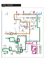
The demodulator IC (IC191) contains the 3rd mixer, limiter
amplifier, quadrature detector, active filter and noise amplifier, etc.
The switched signals from the mode switch (IC342, pin 1)
are applied to the LOGIC-1 unit via J1801 (pin 20).
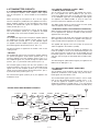
The amplified signal from the IF amplifier (Q191) is applied
to the 3rd mixer section of the demodulator IC (IC191, pin
16) and is then mixed with the 3rd LO signal to be converted
into the 450 kHz 3rd IF signal. The 3rd IF signal from the
3rd mixer section (IC191, pin 3) passes through the ceramic
filter (FI193) via the mode switches (D192, D193) to remove
unwanted heterodyned frequencies. The filtered signal is
amplified at the limiter amplifier section (IC191, pin 5) and
then applied to the quadrature detector section (IC191, pins
10, 11) to demodulate the digital audio signals.
• FM MODE
The same demodulator IC that is used for DV mode operation is used for FM demodulation.
The amplified signal from the IF amplifier (Q191) is applied
to the 3rd mixer section of the demodulator IC (IC191, pin
16) and is then mixed with the 3rd LO signal to be converted
into the 450 kHz 3rd IF signal. The 3rd IF signal from the
3rd mixer section (IC191, pin 3) passes through the ceramic
filter (FI192) via the mode switches (D192, D193) to remove
unwanted heterodyned frequencies. The filtered signal is
amplified at the limiter amplifier section (IC191, pin 5) and
then applied to the quadrature detector section (IC191, pins
10, 11) to demodulate the AF signals.
The 3rd LO signal (30.6 MHz) is produced at the 1st PLL
circuit by doubling it’s reference frequency (X400: 15.3 MHz)
at the doubler (Q550).
The digital audio signals from the demodulator IC (IC191, pin
9) are amplified at IC343 (pins 6, 7) and then applied to the
mode switch (IC342, pins 1, 7).
The AF signals are output from the demodulator IC (IC191,
pin 9) and are then applied to the AF amplifier circuit.
The switched signals from the mode switch (IC342, pin 1)
are applied to the LOGIC-1 unit via J1801 (pin 20).
4-1-6 DIGITAL CIRCUITS (LOGIC-1 UNIT)
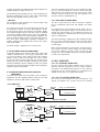
The digital circuits convert the demodulated digital audio
signals into the analog audio signals and convert the
demodulated data signals format for PC communication via
the USB controller (for DV mode: low speed data operation)
or Ethernet controller (for DD mode).
• DD MODE
The MSK receiver IC (IC271) contains the limiter amplifier,
quadrature detector, etc.
The amplified signal from the IF amplifier (Q271) is applied
to the limiter amplifier section of the MSK receiver IC (IC271,
pin 7) and then applied to the quadrature detector section
(IC271, pin 11) to demodulate to the data signals.
The demodulated digital audio or data signals from the
mode switch (MAIN unit: IC342, pin 1) are applied to the
GMSK MODEM IC (IC150, pin 11). The applied signals are
synchronized with the clock signal, then the synchronized
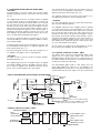
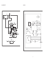
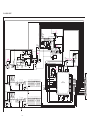
• 3RD IF AND DEMODULATOR CIRCUIT (DV/FM MODE)
FI192 (FM mode)
3rd IF filters
450 kHz
30.6 MHz
8
FI193 (DV mode)
Noise
amp.
5
7
Active
filter
Limiter
amp.
9
2
Mixer
RSSI
10
12
11
AF signals
5V
X191 Discriminator
Q550
2
X400
15.3 MHz
Noise
detector
Quadrature
detector
3
BPF
IC191
TA31136FN
14
16
2nd IF from the IF amplifier (Q191)
“NOIS” signal to the CPU (LOGIC-1 unit; IC50)
“A_RS” signal to the CPU (LOGIC-1 unit; IC50)
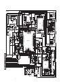
• DIGITAL CIRCUITS (LOGIC-1 UNIT)
RECEIVED SIGNAL
From
GMSK
demodulator
MODEM
IC150
circuit (IC342)
To modulator
circuit (IC831)
FPGA
IC200
AMBE
CODEC
IC2
CPU
IC50
LINER
CODEC
IC1
To AF amplifier circuit
(MAIN unit; IC1411)
From
MIC amplifier circut
(MAIN unit; IC1671)
BASEBAND
FILTER
TRANSMIT SIGNAL
4-2