1
SERVICE
MANUAL
STEREO/DUAL 31-BAND GRAPHIC
EQUALIZER
GEQ-1231D/2231D
www.inter-m.com
MADE IN KOREA
2003.2 9017100300
MICOM DATA
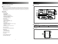
MM74HC4051 8-CHANNEL ANALOG MULTIPLEXER
GENERAL DESCRIPTION
The MM74HC4051, MM74HC4052 and MM74HC4053 Multiplexers are digitally controlled analog switches
implemented in advanced silicon-gate CMOS technology. These switches have low “on” resistance and
low “off” leakages. They are bidirectional switches, thus any analog input may be used as an output and
vice-versa. Also These switches contain linearization circuity which lowers the on resistance and increases
switch linearity. These devices allow control of up to ± 6V(peak) analog signals with digital control signals
of 0 to 6V. Three supply pins are provided for VCC, ground, and VEE. This enables the connection of 0-5V
logic signals when VCC = 5V and an analog input range of ± 5V when VEE = 5V. All three devices also have
an inhibit control which when HIGH will disable all switches to their off state. All analog inputs and outputs
and digital inputs are protected from electrostatic damage by diodes to VCC and ground.
This device connects together the outputs of 8 switches, thus achieving an 8 channel multiplexer. The
binary code placed on the A, B, and C select lines determines which one of the eight switches is “on”, and
connects one of the eight inputs to the common output.
FEATURES
• Wide analog input voltage range: ±6V
• Low on resistance: 50 typ.(VCC-VEE = 4.5V), 30 typ.(VCC-VEE = 9V)
• Logic level translation to enable 5V logic with ± 5V analog signals
• Low quiescent current: 80µA maximum (74HC)
• Matched Switch characteristic
ORDERING CODE:
Order Number
MM74HC4051M
MM74HC4051WM
MM74HC4051SJ
MM74HC4051MTC
MM74HC4051N
Package Number
M16A
M16B
M16D
MTC16
N16E
Package Description
16-Lead Small Outline Integrated Circuit (SOIC), JEDEC MS-012,0.150˝ Narrow
16-Lead Small Outline Integrated Circuit (SOIC), JEDEC MS-013,0.300˝ Wide
16-Lead Small Outline Package (SOP), ELAJ TYPE ll, 5.3mm Wide
16-Lead Thin Shrink Small Outline Package (TSSOP), JEDEC MO-153,4.4mm Wide
16-Lead Plastic Dual-In-Line Package (PDIP), JEDEC MS-0010.300˝ Wide
Devices also available in Tape and Reel. Specify by appending the suffix letter X to the ordering code.
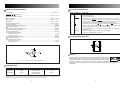
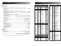
CONTENTS
Micom Data
Specifications
Electrical Parts List
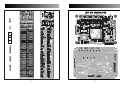
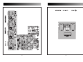
Top and Bottom View of P.C. Board
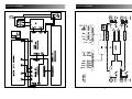
Wiring Diagram
Block Diagram
Schematic Diagram
Exploded View of Cabinet & Chassis / Mechanical Parts List
Ass’y Drawing
1 ~ 21
22
23 ~ 24
25 ~ 29
30
31~ 32
33 ~ 50
51 ~ 54
55 ~ 58
1
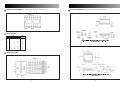
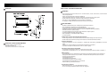
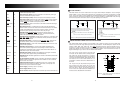
CONNECTION DIAGRAMS (Pin Assignments for DIP, SOIC, SOP and TSSO)
PHYSICAL DIMENSIONS inches (millimeters) unless otherwise noted
Top View
TRUTH TABLES
Inh
H
L
L
L
L
L
L
L
L
Input
C
B
X
X
L
L
L
L
L
H
L
H
H
L
H
L
H
H
H
H
A
X
L
H
L
H
L
H
L
H
“ON”
Channel
None
Y0
Y1
Y2
Y3
Y4
Y5
Y6
Y7
LOGIC DIAGRAMS
2
3
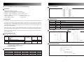
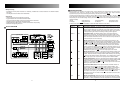
74LV164 8-bit SERIAL-IN / PARALLEL-OUT SHIFT REGISTER
PIN CONFIGURATION
FEATURES
– Wide operating voltage: 1.0 to 5.5V
– Optimized for Low Voltage applications: 1.0 to 3.6V
– Accepts TTL input levels between VCC=2.7V and VCC=3.6V
– Typical VOLP (output ground bounce) < 0.8V@VCC=3.3V, Tamb=25°C
– Typical VOHV (output VOH undershoot) > 2V@VCC=3.3V, Tamb=25°C
– Gated serial data inputs
– Output capability: standard
– Asynchronous master reset
– ICC category: MSl
SV00381
PIN DESCRIPTION
DESCRIPTION
The 74LV164 is a low-voltage Si-gate CMOS device and is pin and function compatible with the 74HC/HCT164.
The 74LV164 is an 8-bit edge-triggered shift register with serial data entry and an output from each of the
eight stages. Data is entered serially through one of two inputs(Dsa or Dsb); either input can be used as an
active HIGH enable for data entry through the other input. Both inputs must be connected together or an
unused input must be tied HIGH.
Data shifts one place to the right on each LOW-to-HIGH transition of the clock (CP) input and enters into Q0,
Pin Number
1, 2
3, 4, 5, 6
10, 11, 12, 13
7
8
9
14
Symbol
Dsa, Dsb
Q0 to Q7
Function
Date inputs
Outputs
GND
CP
MR
VCC
Ground(ov)
Clock input (LOW-to-HIGH, edge-trig-gered)
Master reset input (active LOW)
Positive supply voltage
which is the logical AND of the two data inputs (Dsa, Dsb) that existed one set-up time prior to the rising clock edge.
A LOW on the master reset (MR) input overrides all other inputs and clears the register asynchronously,
forcing all outputs LOW.
LOGIC SYMBOL
LOGIC SYMBOL (IEEE/IEC)
QUICK REFERENCE DATA
GND = OV; Tamb = 25°C; tr=tf ≤ 2.5ns
Symbol
tPHL, tPLH
fmax
Cl
CPD
Parameter
Propagation delay
CP to Qn
MR to Qn
Maximum clock frequency
Input capacitance
Power dissipation capacitance per gate
Conditions
C L=15pF
VCC=3.3V
VCC=3.3V
Notes 1 and 2
Typical
12
12
Unit
ns
78
3.5
40
MH Z
pF
pF
SV00382
SV00383
FUNCTIONAL DIAGRAM
NOTES 1: CPD is used to determine the dynamic power dissipation (PD in µW)
PD = CPD x VCC2 x fi + ∑(CL x VCC2 x fO) where:
fi = input frequency in MHz; CL = output load capacitance in pF;
fO = output frequency in MHz; VCC = supply voltage in V;
∑(CL x VCC2 x fO) = sum of the outputs.
2: The condition is Vl = GND to VCC
ORDERING INFORMATION
Packages
14-Pin Plastic DIL
14-Pin Plastic SO
14-Pin Plastic SSOP Type II
14-Pin Plastic TSSOP Type I
Temperature Range
-40°C to + 125°C
-40°C to + 125°C
-40°C to + 125°C
-40°C to + 125°C
Outside North Amerlca
74LV164N
74LV164D
74LV164DB
74LV164PW
4
North Amerlca
74LV164N
74LV164D
74LV164DB
74LV164PW DH
Pkg. Dwg.#
SOT27-1
SOT108-1
SOT337-1
SOT402-1
SV00384
5
AD7819 2.7V to 5.5V, 200 kSPS 8-bit SAMPLING ADC
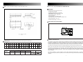
SO14 : plastic small outline package; 14 leads; body width 3.9 mm
FEATURES
– 8-Bit ADC with 4.5 µs Conversion Time
– On-Chip Track and Hold
– Operating Supply Range : 2.7V to 5.5V
– Specifications at 2.7V-3.6V and 5V ± 10%
– 8-Bit Parallel Interface : 8-Bit Read
– Power Performance
Normal Operation : 10.5mW,VDD=3V
– Automatic Power-Down : 57.75µW@1kSPS,VDD=3V
– Analog Input Range : 0V to VREF
– Reference Input Range : 1.2V to VDD
FUNCTIONAL BLOCK DIAGRAM
GENERAL DESCRIPTION
DIMENSIONS (inch dimensions are derived from the original mm dimensions)
A
Unit max.
A1
0.25
mm 1.75 0.10
0.0098
inches 0.069 0.0039
A2
A3
bp
c
D(1)
1.45
0.49 0.25 8.75
0.25
1.25
0.36 0.19 8.55
0.057
0.019 0.0098 0.35
0.049 0.01 0.014 0.0075 0.34
E(1)
e
HE
L
LP
4.0
6.2
1.0
1.27
1.05
3.8
5.8
0.4
0.039
0.16
0.24
0.050
0.041
0.016
0.15
0.23
Q
v
w
y
z(1)
0.7
0.7
0.25 0.25 0.1
0.6
0.3 8°
0.028
0.028 0°
0.01 0.01 0.004
0.024
0.012
NOTE : Plastic or metal protrusions of 0.15 mm maximum per side are not included.
Outline
Version
SOT108-1
Iec
076E06S
References
Jedec
Eiaj
European
Projection
6
When used in its power-down mode, the AD7819 automatically powers down at the end of a conversion
and powers up at the start of a new conversion. This feature significantly reduces the power consumption
of the part at lower throughput rates. The AD7819 can also operate in a high speed mode where the part is
not powered down between conversions. In this mode of operation the part is capable of providing 200
kSPS throughput.
Issue Date
91-08-13
95-01-23
MS-012AB
The AD7819 is a high speed, microprocessor-compatible, 8-bit analog-to-digital converter with a maximum
throughput of 200kSPS. The converter operates off a single 2.7V to 5.5V supply and contains a 4.5µs
successive approximation A/D converter, track/hold circuitry, on-chip clock oscillator and 8-bit wide parallel
interface. The parallel interface is designed to allow easy interfacing to microprocessors and DSPs. Using
only address decoding logic the AD7819 is easily mapped into the microprocessor address space.
The part is available in a small, 16-lead 0.3" wide, plastic dual-in-line package (DIP); in a 6-lead, 0.15"
wide, narrow body small outline IC (SOIC) and in a 16-lead, narrow body, thin shrink small outline package
(TSSOP).
7
ABSOLUTE MAXIMUM RATINGS*
PIN FUNCTION DESCRIPTION
VDD to DGND ..............................................................................................................................-0.3V to + 7V
Pin No.
1
2
3
4
Digital Input Voltage to DGND
(CONVST, RD, CS) ...............................................................................................................-0.3V, VDD + 0.3V
Digital Output Voltage to DGND
(BUSY, DB0-DB7) .................................................................................................................-0.3V, VDD + 0.3V
Mnemonic
VREF
VIN
GND
CONVST
REFIN to AGND ......................................................................................................................-0.3V, VDD + 0.3V
Analog Input ..........................................................................................................................-0.3V, VDD + 0.3V
Storage Temperature Range.................................................................................................-65 to + 150°C
Junction Temperature ........................................................................................................................... 150°C
Plastic DIP Package, Power Dissipation .............................................................................................450mW
JA Thermal Impedance...................................................................................................................105°C/W
Lead Temperature, (Soldering 10 sec)................................................................................................260°C
SOIC Package, Power Dissipation ......................................................................................................450mW
JA Thermal Impedance .....................................................................................................................75°C/W
Lead Temperature, Soldering
Vapor Phase (60 sec) ....................................................................................................................215°C
Infrared (15 sec)............................................................................................................................220°C
SSOP Package, Power Dissipation.....................................................................................................450mW
JA Thermal Impedance ...................................................................................................................115°C/W
Lead Temperature, Soldering
Vapor Phase (60 sec) ....................................................................................................................215°C
Infrared (15 sec).............................................................................................................................220°C
5
6
CS
RD
7
BUSY
8-15
16
DB0-DB7
VDD
Description
Reference Input, 1.2V to VDD.
Analog Input, 0V to VREF.
Analog and Digital Ground.
Convert Start. A low-to-high transition on this pin initiates a 1.5 µs pulse on an
internally generated CONVST signal. A high-to-low transition on this line initiates the
conversion process if the internal CONVST signal is low. Depending on the signal on
this pin at the end of a conversion, the AD7819 automatically powers down.
Chip Select. This is a logic input. CS is used in conjunction with RD to enable outputs.
Read Pin. This is a logic input. When CS is low and RD goes low, the DB7-DB0 leave
their high impedance state and data is driven onto the data bus.
ADC Busy Signal. This is a logic output. This signal goes logic high during the
conversion process.
Data Bit 0 to 7. These outputs are three-state TTL-compatible.
Positive power supply voltage, 2.7V to 5.5V.
PIN CONFIGURATION DIP/SOIC
CAUTION
ESD (electrostatic discharge) sensitive device. Electrostatic charge as high as 4000V
readily accumulate on the human body and test equipment and can discharge
without detection. Although the AD7819 features proprietary ESD protection circuitry,
permanent damage may occur on devices subjected to high-energy electrostatic
discharges, Therefore, proper ESD precaution are recommended to avoid performance degradation or loss of
functionality.
Figure 1. Load Circuit for Digital Output Timing Specifications
ORDERING GUIDE
Model
AD7819YN
AD7819YR
AD7819YRU
Linearity Error(LSB)
± 1 LSB
± 1 LSB
± 1 LSB
Package Description
Plastic DIP
Small Outline IC
Thin Shark Small
Outline (TSSOP)
Package Option
N-16
R-16A
RU-16
*Stresses above those listed under Absolute Maximum Ratings may cause permanent damage to the device. This is a stress rating only;
functional operation of the device at these or any other conditions above those listed in the operational sections of this specification is not
implied. Exposure to absolute maximum rating conditions for extended periods may affect device reliability.
8
9
AK4524 24 bit 96kHz AUDIO CODEC
BLOCK DIAGRAM
GENERAL DESCRIPTION
The AK4524 is a high performance 24bit CODEC for the 96kHz recording system. The ADC has an
Enhanced Dual Bit architecture with wide dynamic range. The DAC uses the new developed Advanced
Multi Bit architecture and achieves low outband noise and high jitter tolerance by use of SCF(switched
capacitor filter) techniques.The AK4524 has an input PGA and is well suited MD, DVTR system and
musical instruments.
FEATURES
• 24bit 2ch ADC
– 64x Oversampling
– Single-End inputs
– S/(N+D):90dB
– Dynamic Range, S/N:100dB
– Digital HPF for offset cancellation
– Input PGA with +8dB gain & 0.5dB step
– Input DATT with -72dB att
– I/F format:MSB justified or I2S
• 24bit 2ch DAC
– 128 x Oversampling
– 24bit 8 times Digital Filter
Ripple:±0.005dB, Attenuation:75dB
– SCF
– Differential Outputs
– S/(N+D):94dB
– Dynamic Range, S/N:110dB
– De-emphasis for 32kHz, 44.1kHz, 48kHz sampling
– Output DATT with -72dB att
– Soft Mute
– I/F format:MSB justified, LSB justified or l2S
ORDERING GUIDE
AK4524VF
AKD4524
-10~+70°C
Evaluation Board
28pin VSOP (0.65mm pitch)
• High Jitter Tolerance
PIN LAYOUT
• 3-wire Serial Interface for Volume Control
• Master Clock
– X’tal Oscillating Circuit
– 256fs/384fs/768fs/1024fs
• Master Mode/Slave Mode
• 5V operation
• 3V Power Supply Pin for 3V I/F
• Small 28pin VSOP package
10
11
PACKAGZ
ADSP-21065L DSP MICROCOMPUTER
SUMMARY
– High Performance Signal Computer for Communications, Audio, Automotive, Instrumentation and
Industrial Applications
– Super Harvard Architecture Computer (SHARC®)
Four Independent Buses for Dual Data, Instruction, and I/O Fetch on a Single Cycle
– 32-Bit Fixed-Point Arithmetic; 32-Bit and 40-Bit Floating-Point Arithmetic
– 544 Kbits On-Chip SRAM Memory and Integrated I/O Peripheral
– I2S Support, for Eight Simultaneous Receive and Transmit Channels
KEY FEATURES
– 66 MIPS, 198 MFLOPS Peak, 132 MFLOPS Sustained Performance
– User-Configurable 544 Kbits On-Chip SRAM Memory
– Two External Port, DMA Channels and Eight Serial Port, DMA Channels
– SDRAM Controller for Glueless Interface to Low Cost External Memory (@66 MHz)
– 64M Words External Address Range
– 12 Programmable I/O Pins and Two Timers with Event Capture Options
– Code-Compatible with ADSP-2106x Family
– 208-Lead MQFP or 196-Ball Mini-BGA Package
– 3.3 Volt Operation
Flexible Data Formats and 40-Bit Extended Precision
– 32-Bit Single-Precision and 40-Bit Extended-Precision IEEE Floating-Point Data Formats
– 32-Bit Fixed-Point Data Format, Integer and Fractional, with Dual 80-Bit Accumulators
Note : Dimension “*” does not include moid flash.
Parallel Computations
– Single-Cycle Multiply and ALU Operations in Parallel with Dual Memory Read/Writes and Instruction
Fetch
– Multiply with Add and Subtract for Accelerated FFT Butterfly Computation
– 1024-Point Complex FFT Benchmark: 0.274 ms (18,221 Cycles)
PACKAGE & LEAD FRAME MATERIAl
Package molding compound: Epoxy
Lead frame material: Cu
Lead frame surface treatment: Solder plate
544 Kbits Configurable On-Chip SRAM
– Dual-Ported for Independent Access by Core Processor and DMA
– Configurable in Combinations of 16-, 32-, 48-Bit Data and Program Words in Block 0 and Block 1
DMA Controller
– Ten DMA Channels–Two Dedicated to the External Port and Eight Dedicated to the Serial Ports
– Background DMA Transfers at up to 66 MHz, in Parallel with Full Speed Processor Execution
– Performs Transfers Between:
Internal RAM and Host
Internal RAM and Serial Ports
Internal RAM and Master or Slave SHARC
Internal RAM and External Memory or I/O Devices
External Memory and External Devices
Host Processor Interface
– Efficient Interface to 8-, 16-, and 32-Bit Microprocessors
– Host Can Directly Read/Write ADSP-21065L IOP Registers
12
13
Multiprocessing
– Distributed On-Chip Bus Arbitration for Glueless, Parallel Bus Connect Between Two ADSP-21065Ls
Plus Host
– 132 Mbytes/s Transfer Rate Over Parallel Bus
Serial Ports
– Independent Transmit and Receive Functions
– Programmable 3-Bit to 32-Bit Serial Word Width
– I2S Support Allowing Eight Transmit and Eight Receive Channels
– Glueless Interface to Industry Standard Codecs
– TDM Multichannel Mode with µ-Law/A-Law Hardware Companding
– Multichannel Signaling Protocol
BLOCK DIAGRAM
14
PIN DESCRIPTIONS
ADSP-21065L pin definitions are listed below. Inputs identified as synchronous (S) must meet timing
requirements with respect to CLKIN (or with respect to TCK for TMS, TDI). Inputs identified as
asynchronous (A) can be asserted asynchronously to CLKIN (or to TCK for TRST).
Unused inputs should be tied or pulled to VDD or GND, except for ADDR23-0, DATA31-0, FLAG11-0, SW, and
inputs that have internal pull-up or pull-down resistors (CPA, ACK, DTxX, DRxX, TCLKx, RCLKx, TMS, and
TDI)–these pins can be left floating. These pins have a logic-level hold circuit that prevents the input from
floating internally.
I=Input
S=Synchronous
P=Power Supply
(O/D)=Open Drain
O=Output
A=Asynchronous
G=Ground
(A/D)=Active Drive
T=Three-state (when SBTS is asserted, or when the ADSP-2106x is a bus slave)
Pin
ADDR23-0
Type
I/O/T
Function
External Bus Address. The ADSP-21065L outputs addresses for external
memory and peripherals on these pins. In a multiprocessor system the bus
master outputs addresses for read/writes of the IOP registers of the other
ADSP-21065L. The ADSP-21065L inputs addresses when a host processor
or multiprocessing bus master is reading or writing its IOP registers.
DATA31-0
I/O/T
External Bus Data. The ADSP-21065L inputs and outputs data and
instructions on these pins. The external data bus transfers 32-bit singleprecision floating-point data and 32-bit fixed-point data over bits 31-0. 16-bit
short word data is transferred over bits 15-0 of the bus. Pull-up resistors on
unused DATA pins are not necessary.
MS3-0
I/O/T
Memory Select Lines. These lines are asserted as chip selects for the
corresponding banks of external memory. Internal ADDR25-24 are decoded
into MS3-0. The MS3-0 lines are decoded memory address lines that change
at the same time as the other address lines. When no external memory
access is occurring the MS3-0 lines are inactive; they are active, however,
when a conditional memory access instruction is executed, whether or not
the condition is true. Additionally, an MS3-0 line which is mapped to SDRAM
may be asserted even when no SDRAM access is active. In a
multiprocessor system, the MS3-0 lines are output by the bus master.
RD
I/O/T
Memory Read Strobe. This pin is asserted when the ADSP-21065L reads
from external memory devices or from the IOP register of another ADSP21065L. External devices (including another ADSP-21065L) must assert RD
to read from the ADSP-21065L’s IOP registers. In a multiprocessor system,
RD is output by the bus master and is input by another ADSP-21065L.
WR
I/O/T
Memory Write Strobe. This pin is asserted when the ADSP-21065L writes
to external memory devices or to the IOP register of another ADSP-21065L.
External devices must assert WR to write to the ADSP-21065L’s IOP
registers. In a multiprocessor system, WR is output by the bus master and is
input by the other ADSP-21065L.
SW
I/O/T
Synchronous Write Select. This signal interfaces the ADSP-21065L to
synchronous memory devices (including another ADSP-21065L). The
ADSP-21065L asserts SW to provide an early indication of an impending
write cycle, which can be aborted if WR is not later asserted (e.g., in a
conditional write instruction). In a multiprocessor system, SW is output by the
bus master and is input by the other ADSP-21065L to determine if the
multiprocessor access is a read or write. SW is asserted at the same time as
the address output.
ACK
I/O/S
Memory Acknowledge. External devices can deassert ACK to add wait
states to an external memory access. ACK is used by I/O devices, memory
controllers, or other peripherals to hold off completion of an external memory
15
Pin
Type
Function
access. The ADSP-21065L deasserts ACK as an output to add wait states to
a synchronous access of its IOP registers. In a multiprocessor system, a
slave ADSP-21065L deasserts the bus master’s ACK input to add wait
state(s) to an access of its IOP registers. The bus master has a keeper latch
on its ACK pin that maintains the input at the level to which it was last driven.
Pin
Type
Function
access. The ADSP-21065L deasserts ACK as an output to add wait states to
a synchronous access of its IOP registers. In a multiprocessor system, a
slave ADSP-21065L deasserts the bus master’s ACK input to add wait
state(s) to an access of its IOP registers. The bus master has a keeper latch
on its ACK pin that maintains the input at the level to which it was last driven.
SBTS
I/S
Suspend Bus Three-State. External devices can assert SBTS to place the
external bus address, data, selects, and strobes–but not SDRAM control
pins–in a high impedance state for the following cycle. If the ADSP-21065L
attempts to access external memory while SBTS is asserted, the processor
will halt and the memory access will not finish until SBTS is deasserted.
SBTS should only be used to recover from host processor/ADSP-21065L
deadlock.
SBTS
I/S
Suspend Bus Three-State. External devices can assert SBTS to place the
external bus address, data, selects, and strobes–but not SDRAM control
pins–in a high impedance state for the following cycle. If the ADSP-21065L
attempts to access external memory while SBTS is asserted, the processor
will halt and the memory access will not finish until SBTS is deasserted.
SBTS should only be used to recover from host processor/ADSP-21065L
deadlock.
IRQ2-0
I/A
Interrupt Request Lines. May be either edge-triggered or level-sensitive.
IRQ2-0
I/A
Interrupt Request Lines. May be either edge-triggered or level-sensitive.
FLAG11-0
I/O/A
Flag Pins. Each is configured via control bits as either an input or an output.
As an input, it can be tested as a condition. As an output, it can be used to
signal external peripherals.
FLAG11-0
I/O/A
Flag Pins. Each is configured via control bits as either an input or an output.
As an input, it can be tested as a condition. As an output, it can be used to
signal external peripherals.
HBR
I/A
Host Bus Request. Must be asserted by a host processor to request control
of the ADSP-21065L’s external bus. When HBR is asserted in a
multiprocessing system, the ADSP-21065L that is bus master will relinquish
the bus and assert HBG. To relinquish the bus, the ADSP-21065L places the
address, data, select, and strobe lines in a high impedance state. It does,
however, continue to drive the SDRAM control pins. HBR has priority over all
ADSP-21065L bus requests (BR2-1) in a multiprocessor system.
HBR
I/A
Host Bus Request. Must be asserted by a host processor to request control
of the ADSP-21065L’s external bus. When HBR is asserted in a
multiprocessing system, the ADSP-21065L that is bus master will relinquish
the bus and assert HBG. To relinquish the bus, the ADSP-21065L places the
address, data, select, and strobe lines in a high impedance state. It does,
however, continue to drive the SDRAM control pins. HBR has priority over all
ADSP-21065L bus requests (BR2-1) in a multiprocessor system.
HBG
I/O
Host Bus Grant. Acknowledges an HBR bus request, indicating that the
host processor may take control of the external bus. HBG is asserted by the
ADSP-21065L until HBR is released. In a multiprocessor system, HBG is
output by the ADSP-21065L bus master.
HBG
I/O
Host Bus Grant. Acknowledges an HBR bus request, indicating that the
host processor may take control of the external bus. HBG is asserted by the
ADSP-21065L until HBR is released. In a multiprocessor system, HBG is
output by the ADSP-21065L bus master.
CS
I/A
Chip Select. Asserted by host processor to select the ADSP-21065L.
CS
I/A
Chip Select. Asserted by host processor to select the ADSP-21065L.
REDY(O/D)
O
Host Bus Acknowledge. The ADSP-21065L deasserts REDY to add wait
states to an asynchronous access of its internal memory or IOP registers by
a host. Open drain output (O/D) by default; can be programmed in ADREDY
bit of SYSCON register to be active drive (A/D). REDY will only be output if
the CS and HBR inputs are asserted.
REDY(O/D)
O
Host Bus Acknowledge. The ADSP-21065L deasserts REDY to add wait
states to an asynchronous access of its internal memory or IOP registers by
a host. Open drain output (O/D) by default; can be programmed in ADREDY
bit of SYSCON register to be active drive (A/D). REDY will only be output if
the CS and HBR inputs are asserted.
DMAR1
I/A
DMA Request 1 (DMA Channel 9).
DMAR1
I/A
DMA Request 1 (DMA Channel 9).
DMAR2
I/A
DMA Request 2 (DMA Channel 8).
DMAR2
I/A
DMA Request 2 (DMA Channel 8).
DMAG1
O/T
DMA Grant 1 (DMA Channel 9).
DMAG1
O/T
DMA Grant 1 (DMA Channel 9).
DMAG2
O/T
DMA Grant 2 (DMA Channel 8).
DMAG2
O/T
DMA Grant 2 (DMA Channel 8).
BR2-1
I/O/S
Multiprocessing Bus Requests. Used by multiprocessing ADSP-21065L’s
to arbitrate for bus mastership. An ADSP-21065L drives its own BRx line
(corresponding to the value of its ID2-0 inputs) only and monitors all others. In
a uniprocessor system, tie both BRx pins to VDD.
BR2-1
I/O/S
Multiprocessing Bus Requests. Used by multiprocessing ADSP-21065L’s
to arbitrate for bus mastership. An ADSP-21065L drives its own BRx line
(corresponding to the value of its ID2-0 inputs) only and monitors all others. In
a uniprocessor system, tie both BRx pins to VDD.
ID1-0
I
Multiprocessing ID. Determines which multiprocessor bus request
(BR1–BR2) is used by ADSP-21065L. ID=01 corresponds to BR1, ID=10
corresponds to BR2. ID=00 in single-processor systems. These lines are a
system configuration selection which should be hard-wired or changed only
at reset.
ID1-0
I
Multiprocessing ID. Determines which multiprocessor bus request
(BR1–BR2) is used by ADSP-21065L. ID=01 corresponds to BR1, ID=10
corresponds to BR2. ID=00 in single-processor systems. These lines are a
system configuration selection which should be hard-wired or changed only
at reset.
CPA (O/D)
I/O
Core Priority Access. Asserting its CPA pin allows the core processor of an
ADSP-21065L bus slave to interrupt background DMA transfers and gain
CPA (O/D)
I/O
Core Priority Access. Asserting its CPA pin allows the core processor of an
ADSP-21065L bus slave to interrupt background DMA transfers and gain
16
17
Pin
TMS
Type
I/S
Function
Test Mode Select (JTAG). Used to control the test state machine. TMS has
a 20kΩ internal pull-up resistor.
TDI
I/S
Test Data Input (JTAG). Provides serial data for the boundary scan logic.
TDI has a 20kΩ internal pull-up resistor.
TDO
O
Test Data Output (JTAG). Serial scan output of the boundary scan path.
TRST
I/A
Test Reset (JTAG). Resets the test state machine. TRST must be asserted
(pulsed low) after power-up or held low for proper operation of the ADSP21065L. TRST has a 20kΩ internal pull-up resistor.
EMU (O/D)
O
Emulation Status. Must be connected to the ADSP-21065L EZ-ICE target
board connector only.
BMSTR
O
Bus Master Output. In a multiprocessor system, indicates whether the
ADSP-21065L is current bus master of the shared external bus. The ADSP21065L drives BMSTR high only while it is the bus master. In a singleprocessor system (ID=00), the processor drives this pin high.
CAS
I/O/T
SDRAM Column Access Strobe. Provides the column address. In
conjunction with RAS, MSx, SDWE, SDCLKx, and sometimes SDA10,
defines the operation for the SDRAM to perform.
RAS
I/O/T
SDRAM Row Access Strobe. Provides the row address. In conjunction with
CAS, MSx, SDWE, SDCLKx, and sometimes SDA10, defines the operation
for the SDRAM to perform.
SDWE
I/O/T
SDRAM Write Enable. In conjunction with CAS, RAS, MSx, SDCLKx and
sometimes SDA10, defines the operation for the SDRAM to perform.
DQM
O/T
SDRAM Data Mask. In write mode, DQM has a latency of zero and is used
to block write operations.
SDCLK1-0
I/O/S/T
SDRAM 2x Clock Output. In systems with multiple SDRAM devices
connected in parallel, supports the corresponding increased clock load
requirements, eliminating need of off-chip clock buffers. Either SDCLK1 or
both SDCLKx pins can be three-stated.
SDCKE
I/O/T
SDRAM Clock Enable. Enables and disables the CLK signal. For details,
see the data sheet supplied with your SDRAM device.
SDA10
O/T
SDRAM A10 Pin. Enables applications to refresh an SDRAM in parallel with
a host access.
XTAL
O
Crystal Oscillator Terminal. Used in conjunction with CLKIN to enable the
ADSP-21065L’s internal clock generator or to disable it to use an external
clock source. See CLKIN.
I/O/A
PWM Output/Event Capture. In PWMOUT mode, is an output pin and
functions as a timer counter. In WIDTH_CNT mode, is an input pin and
functions as a pulse counter/event capture.
PWM_EVENT1-0
VDD
P
Power Supply; nominally +3.3V dc. (33 pins)
GND
G
Power Supply Return. (37 pins)
NC
Do Not Connect. Reserved pins that must be left open and unconnected. (7)
CLOCK SIGNALS
The ADSP-21065L can use an external clock or a crystal. See CLKIN pin description. You can configure the
ADSP-21065L to use its internal clock generator by connecting the necessary components to CLKIN and
XTAL. You can use either a crystal operating in the fundamental mode or a crystal operating at an overtone.
Figure shows the component connections used for a crystal operating in fundamental mode, and Figure 2
shows the component connections used for a crystal operating at an overtone.
SUGGESTED COMPONENTS FOR 30 MHz OPERATION:
ECLIPTEK EC2SM-T-30.000M (SURFACE MOUNT PACKAGE)
ECLIPTEK ECT-30.000M (THRU-HOLE PACKAGE)
C1=18pF
C2=27pF
C3=75pF
L1=3300nH
Rs=SEE NOTE.
NOTE: C1, C2, C3, Rs AND L1 ARE SPECIFIC TO CRYSTAL SPECIFIED
FOR X1.
CONTACT MANUFACTURER FOR DETAILS.
SUGGESTED COMPONENTS FOR 30 MHz OPERATION:
ECLIPTEK EC2SM-33-30.000M (SURFACE MOUNT PACKAGE)
ECLIPTEK EC-33-30.000M (THRU-HOLE PACKAGE)
C1=33pF
C2=27pF
NOTE: C1 AND C2 ARE SPECIFIC TO CRYSTAL SPECIFIED FOR
X1.
CONTACT CRYSTAL MANUFACTURER FOR DETAILS.
Figure 1. 30 MHz Operation (Fundamental Mode Crystal)
Figure 2. 30 MHz Operation (3rd Overtone Crystal)
TARGET BOARD CONNECTOR FOR EZ-ICE PROBE
The ADSP-2106x EZ-ICE emulator uses the IEEE 1149.1 JTAG test access port of the ADSP-2106x to
monitor and control the target board processor during emulation. The EZ-ICE probe requires the ADSP2106x’s CLKIN, TMS, TCK, TRST, TDI, TDO, EMU and GND signals be made accessible on the target
system via a 14-pin connector (a 2 row x 7 pin strip header) such as that shown in Figure 3. The EZ-ICE
probe plugs directly onto this connector for chip-on-board emulation. You must add this connector to your
target board design if you, intend to use the ADSP-2106x EZ-ICE.
The total trace length between the EZ-ICE
connector and the furthest device sharing the EZICE JTAG pins should be limited to 15 inches
maximum for guaranteed operation. This restriction
on length must include EZ-ICE JTAG signals, which
are routed to one or more 2106x devices or to a
combination of 2106xs and other JTAG devices on
the chain.
The 14-pin, 2-row pin strip header is keyed at the
Pin 3 location–you must remove Pin 3 from the
header. The pins must be 0.025 inch square and at
least 0.20 inch in length. Pin spacing should be
0.1x0.1 inches. Pin strip headers are available from
vendors such as 3M, McKenzie and Samtec.
Figure 3. Target Board Connector for ADSP-2106x
EZ-ICE (JTAG Header)
18
19
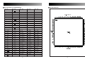
208-LEAD MQFP PIN CONFIGURATION
208-LEAD MQFP PIN
Pin Pin
No. Name
Pin
No.
Pin
Name
Pin
No.
Pin
Name
Pin
No.
Pin
Name
Pin
No.
Pin
Name
1
2
3
4
5
6
7
8
9
10
11
12
13
14
15
16
17
18
19
20
21
22
23
24
25
26
27
28
29
30
31
32
33
34
35
36
37
38
39
40
41
42
43
44
45
46
47
48
49
50
51
52
53
54
55
56
57
58
59
60
61
62
63
64
65
66
67
68
69
70
71
72
73
74
75
76
77
78
79
80
81
82
83
84
CAS
SDWE
VDD
DQM
SDCKE
SDA10
GND
DMAG1
DMAG2
HBG
BMSTR
VDD
CS
SBTS
GND
WR
RD
GND
VDD
GND
REDY
SW
CPA
VDD
VDD
GND
ACK
MS0
MS1
GND
GND
MS2
MS3
FLAG11
VDD
FLAG10
FLAG9
FLAG8
GND
DATA0
DATA1
DATA2
85
86
87
88
89
90
91
92
93
94
95
96
97
98
99
100
101
102
103
104
105
106
107
108
109
110
111
112
113
114
115
116
117
118
119
120
121
122
123
124
125
126
VDD
DATA3
DATA4
DATA5
GND
DATA6
DATA7
DATA8
VDD
GND
VDD
DATA9
DATA10
DATA11
GND
DATA12
DATA13
NC
NC
DATA14
VDD
GND
DATA15
DATA16
DATA17
VDD
DATA18
DATA19
DATA20
GND
NC
DATA21
DATA22
DATA23
GND
VDD
DATA24
DATA25
DATA26
VDD
GND
DATA27
127
128
129
130
131
132
133
134
135
136
137
138
139
140
141
142
143
144
145
146
147
148
149
150
151
152
153
154
155
156
157
158
159
160
161
162
163
164
165
166
167
168
DATA28
DATA29
GND
VDD
VDD
DATA30
DATA31
FLAG7
GND
FLAG6
FLAG5
FLAG4
GND
VDD
VDD
NC
ID1
ID0
EMU
TDO
TRST
TDI
TMS
GND
TCK
BSEL
BMS
GND
GND
VDD
RESET
VDD
GND
ADDR23
ADDR22
ADDR21
VDD
ADDR20
ADDR19
ADDR18
GND
GND
169
170
171
172
173
174
175
176
177
178
179
180
181
182
183
184
185
186
187
188
189
190
191
192
193
194
195
196
197
198
199
200
201
202
203
204
205
206
207
208
ADDR17
ADDR16
ADDR15
VDD
ADDR14
ADDR13
ADDR12
VDD
GND
ADDR11
ADDR10
ADDR9
GND
VDD
ADDR8
ADDR7
ADDR6
GND
GND
ADDR5
ADDR4
ADDR3
VDD
VDD
ADDR2
ADDR1
ADDR0
GND
FLAG0
FLAG1
FLAG2
VDD
FLAG3
NC
NC
GND
IRQ0
IRQ1
IRQ2
NC
VDD
RFS0
GND
RCLK0
DR0A
DR0B
TFS0
TCLK0
VDD
GND
DT0A
DT0B
RFS1
GND
RCLK1
DR1A
DR1B
TFS1
TCLK1
VDD
VDD
DT1A
DT1B
PWM_EVENT1
GND
PWM_EVENT0
BR1
BR2
VDD
CLKIN
XTAL
VDD
GND
SDCLK1
GND
VDD
SDCLK0
DMAR1
DMAR2
HBR
GND
RAS
20
21
SPECIFICATIONS
ELECTRICAL PARTS LIST
Ref No.
ELECTRICAL
Part No.
Description
Value
AC INPUT B'D (4003482620)
• ANALOG INPUT
XLR & 1/4˝ TRS, Electronically Balanced, RF Filtered, and fully unbalanced compatible
Impedance .......................................................................................................................................>10kΩ
Maximal Input Level .........................................................................................................................20dBu
• ANALOG OUTPUT
XLR & 1/4˝ TRS, Electronically Balanced, RF Filtered and fully unbalanced compatible
Impedance ......................................................................................................................................< 100Ω
Maximum Output Level @ > 600Ω ...................................................................................................20dBu
DIP Switch Selectable Output Attenuator in 3dB Steps ...................20dBu to 2dBu and Unity-Gain Mode
• GRAPHIC EQUALIZER
31-Band 1/3-Octave Interpolating Constant-Q Filter Bank
Selectable Boost/Cut Range ..........................±12dB/ ±6dB and 0 to -12dB/ 0 to -6dB (in Cut Only mode)
Input Gain Control .....................................................................................................................0 to +18dB
6-LED Input Level Meter ..................................-40dBu, -24dBu, -15dBu, -8dBu,- 3dBu, Peak (> +18dBu)
• CUT FILTERS
Low-Cut Frequency Range .................................................................................................12.5Hz~200Hz
Low-Cut Slope .....................................................................................................18dB/octave Butterworth
High-Cut Frequency Range ..............................................................................................3.3kHz~29.5kHz
High-Cut Slope ....................................................................................................18dB/octave Butterworth
• PEAK-LIMITER
Type ......................................................................................................................Maximizer with Soft Clip
Threshold ..................................................................................................................................0 to 19dBu
3-LED Gain Reduction Meter .......................................................................................................1, 3, 6dB
Output Clip Indicator ...................................................................................................................> +19dBu
Limiter Link (GEQ-2231D only) .....................................................................................................ON/OFF
Channel Link (GEQ-2231D only) ..................................................................................................ON/OFF
• SYSTEM PERFORMANCE
Frequency Response (-0.5dB) ............................................................................................10Hz~31.5kHz
Dynamic Range .......................................................................................................................... > 95dB-A
THD+N ........................................................................................................................................< 0.003%
GENERAL
• Power Source .....................................................................................AC 100V/120V/230V/240V, 50/60Hz
• Power Consumption ..............................................................................................................................10W
• Weight ............................................................................................................................GEQ-1231D: 3.5kg
........................................................................................................................................GEQ-2231D: 5.0kg
• Dimensions ...........................................................GEQ-1231D (1HU Rack): 482(W) 44(H) 280(D) mm
.............................................................................. GEQ-2231D (2HU Rack): 482(W) 88(H) 280(D) mm
C402-403
C404-405
TR301
P1 P3 P14 P27
3549222091
3549472092
2658399940
4465998210
4458999110
CAP DE7100F 222MVAI-KC
CAP DE7100F472MVAI-KC
COMON MODE CHOKE COIL MEQ-2000
TERMINAL(250)PCB TAB
FUSE CLIP 5*20
2.2n/250
4.7n/250
CHOKE COIL
TERMINAL
FUSE CLIP
FRONT B'D:GEQ-2231D (4003482400)
IC115-116
C110-140 C142-197
C202-207 C209-211
C101-102
F101
C201 C208
IC106-114
IC101-105 IC120
D101-103 D142
D6 D8-13 D104-111
D120-122 D128 D140
D116-117 D132-133
D14 D113 D123-124
D114 D129-131
D115 D141
D126-127 D118-119
D112 D125
R102 R133
R104-119 R211-221
R223-225 R240-242
R101 R103
R135-158 R165-210
R230 R243
T101-108
Q101-103
SVR101-116
SVR119-132
SVR134-167
SVR168-173
J101
S21225165401 IC 74LCX 138(SOP16)PHI
74LCX138
S35101045039 CAP X7R 100N 10% 63V 2012
100n
S35102204321
S39006999944
S34121000422
S21225160201
S21224147701
S22400502001
CAP CL 22PF 50V J 1608
EMI NFM60(SMD)
CAP RC 10UF 16V
IC 74HC4051 SOIC
IC 74LV164 SOT108-1
DIODE BAW56 SOT23
22p
NFM60R
10u
74HC4051
74LVC164
BAW56
2309770100
LED BL-S4548-TBS22A 1.8MM
LED1.8MM
2300031100
LED LTL-1CHY LITEON
LED3MM-YELLOW
2300032100
LED LTL-1CHG LITEON
LED3MM-GREEN
2300030000
LED LTL-1CHEE LITEON
LED3MM-RED
30101017121
RES TF 100 1/16W 1608
100
30101517121
RES TF 150 1/16W 1608
150
30101027121
RES TF 1K 1/16W 1608
1K
4628980110
PUSH SWITCH
S20510482001 TR MMBT4124 SOT-23
PUSH S/W
mmBT4124
3238010324
VR RS20111D6 10KB ALP
SVR 10KB
3208010324
S44410510626
4355735800
VR RK09K11330CC9 10KB ALP
CON FFC/FPC 26P ZIP ANGLE
FLAT CABLE 1.0 140MM 26P
VR 10KB
CON 26P
ASS'Y
FRONT B'D:GEQ-1231D (400382500)
IC110
C108-112 C117-156
C158-161 C163
C100-101
F101
J101
C157 C162
IC105-109
IC101-103
D117-118
D1-3 D100-102
D103-104 D110-112
D109 D105-107
D115-116
D113-114
R118 R155
R101-116
R100 R123-154
R157-160
T101-103
Q101
SVR101-132
SVR133-135
J101
S21225165401 IC 74LCX 138M (SOP16) FSC
74LCX138
S35101045039 CAP X7R 100N 10% 63V 2012
100n
S35102204321
S39006999944
S44410510626
S34121000632
S21225160201
S21224147701
S22400502001
S20510482001
2300032100
CAP CL 22PF 50V J 1608
EMI NFM60(SMD)
CON FFC/FPC 26P ZIP ANGLE
CAP RC 10UF 25V
IC 74HC4051 SOIC
IC 74LV164 SOT108-1
DIODE BAW56 SOT-23
LED BL-S4548-TBS22A 1.8MM
LED LTL-1CHG LITEON
22p
NFM60R
WAFER 26P
10u
74HC4051
74LV164
BAW56
LED1.8MM
LED3MM-GREEN
2300030000
LED LTL-1CHEE LITEON
LED3MM-RED
2300031100
LED LTL-1CHY LITEON
S30101017121 RES TF 100 1/16W 1608
S30101517121 RES TF 150 1/16W 1608
LED3MM-YELLOW
100
150
PUSH SWITCH
TR MMBT4124 SOT-23
VR RS20111D6 10KB
VR RK09K11330CC9 10KB
CON FFC/FPC 26P ZIP ANGLE
FLAT CABLE 1.0 80MM 26P
DS701
4698099610
4355738616
SW DIP 4 WAY JEC
CON ASS'Y 5P 360MM
PUSH S/W
mmBT4124
SVR 10KB
VR 10KB
CON 26P
ASS'Y
DIP SW
ASS'Y
POWER/IN-OUT B'D (4003482600)
IC401
AC101
BD401
C301-303 C307-309
C412-413 C416-417
C423 C425 C429
22
2168640988
4308991810
2058100976
3609104120-T
3689104219
IC 7815 SAMSUNG
AC CORD DOM 12A INLET
DIODE BRIDGE KBP202G/KBP203G
CAP MA 0.1UF 100V J
CAP X7R 100N 10% 63V (LS5.08)
CAP CE SL 100PF 50V J
CAP X7R 10N 10% 50V (LS5.08)
CAP X7R 1N 10% 50V (LS5.08)
CAP CE SL 330PF 50V J
LW5267/LWB0640/2.5MM-05P
LW5267/LWB0640/2.5MM-02P
LW5267/LWB0640/2.5MM-07P
CON WAFER A2505WV2-07P
EMI FILTER 2200PF
DIODE RECTIFIER LT1N4006(4007)
100p
10n
1n
330P
WAFER 5P
WAFER 2P
WAFER 3P
WAFER 7P
22nF
1N 4006
2058304100
2058100890
3409210033-T
3409210059-T
3408210233
3419533265
3419568238
2648609900
DIODE IN4148M
DIODE RECTIFIER IN5401
CAP E SE 10UF 16V 4*5
CAP RG 10UF 50V 105C
CAP RSD 1000UF 16V SNAP 10P
CAP HC 3300UF 35V
CAP AF HM 6800UF 16V 25P LUG
FERITE BEAD H5B
5508212233
4458999110
4408194510
4408194610
4408194210
2168640979
2168640987
2118089926
FUSE NB 20MM 1A/250V U/C
FUSE CLIP 5*20
XLR JACK (F) (E303A0070N)
XLR JACK (M) (E403A0090N)
XLR JACK(M) E503A0130N
IC LM311N (DIL8) FSC
IC 7915 SAMSUNG
IC LM 350T
1N 4148
1N5401
10/16
10/50
1000/16
3300/35
6800/16
FERRITE
0.125A/250V
1AT
FUSE CLIP
XLR JACK (F)
XLR JACK (M)
JACK PHONE
LM311N
7915
LM350T
4235007210
GND TERMINAL (POWER B'D)
GND TERMINAL
4465998210
TERMINAL(250)PCB TAB
TERMINAL TAB
4428590423
PIN HEADER 2X3POL (LS2.54)
3004100953
3001100953
3005100953
3002150953
3003220953
3003274953
3002220953
RES CF 100 1/5W FN SMA-4000
RES CF 100K 1/5W F N
RES CF 10 1/5W F N
RES CF 15K 1/5W F N
RES CF 2.2K 1/5W F N
RES CF 2.7K 1/5W F N
RES CF 22K 1/5W F N
pinheader 3p
PT
100 1%
100K 1%
10 1%
15K 1%
2.2K
2.7K 1%
22K 1%
3003330953
3003348953
3004390953
3004240953
3003470953
3002470953
3004470953
3009564973
5528007800
4625995510
4648099310
2128612400
2008405980-T
RES CF 3.3K 1/5W F N
RES CF 3.48K 1/5W FN SMA-4000
RES CF 390 1/5W FN
RES CF 240 1/5W FN
RES CF 4.7K 1/5W F N
RES CF 47K 1/5W F N
RES 470 1/5W FN
RES CF 560K 1/5W J N
RELAY AZ850-12 DC12V
SW SLIDE SSAF122NB011(9MM)
POWER SWITCH (H8500VB)
IC TL431CLP (TO92) TIA
KRA103M-AT
3.3K 1%
3.48K 1%
390 1%
240 1%
4.7K 1%
47K 1%
470 1%
560K
RELAY DC12V
SW SLIDE(9MM)
POWER SW
TL431
KRC103M
IC605
2IC620-621
C529-530 C535-536
C538-542 C545-549
C606-630 C650-651
C655-659 C670-677
C683-684
C654
C505 C507 C510 C512
C531-532
C601-603
C604
C525-526 C551-552
C503-504 C513-514
C524 C527 C550
C553 C506 C511
C518-521 C556-559
C605
CN501 CN503-506
CN502
DIP S/W B'D (4003481200)
* Due to continuous improvements specifications and design are subject to change without prior notice.
Part No.
3509101130-T
3689103219
3689102219
3509331130-T
4428595005
4428595002
4428595003
4428595007
3908609980
2058100996
Description
Value
SHT B'D (4003482700)
S30101027121 RES TF 1K 1/16W 1608
4628980110
S20510482001
3238010324
3208010324
S44410510626
4355735900
Ref No.
C427
C433-436
C428 C432
C310-317
CN401-402
CN305 CN403 CN405
CN301-304 CN406
CN404
F402
D301-302 D401-402
D405 D406
D407
D403-404
C426
C430-431
C414-415 C424
C410-411
C422
FB301-308
FS401
FS402-403
FS404
JX302 JX304
JX301 JX303
JK301-304
IC405
IC402
IC404
48
CN407
P32 P36 P38-39
P41-42
P401-404
JP1-2
JP301-304
PT1
R408
R403 R418
R417 R425
R420
R423
R409
R410-411 R416 R419
R421
R404
R406
R401
R402
R413
R407
R415
R405
RLY301-302
SW301-302
S401
IC406
Q401-402
7815
AC INPUT
KBP02
0.1u
100n
23
S21281169601 IC AD7819 8BIT SAMPLING ADC
S22300502001 DIODE BAT54S SOT-23
AD7819
BAT54S
S35101045039 CAP X7R 100N 10% 63V 2012
100n
S35101025039
S35101014331
S35201005020
S35102204339
S35102704321
S35203314030
1N
100P NPO
10p NPO
22P
27P
330P
CAP NPO 1N 10% 63V 2012
CAP CE C 100PF 50V J 0805(2012)
CAP NPO 10p 10% 63V SMD
CAP CL 22PF 50V J 2012
CAP CE C 27PF 50V J 0603(1608)
CAP NPO 330P 5% 50V 2012
S35203324030 CAP NPO 3.3N 5% 50V 2012
3.3N
S35103304321 CAP CL 33PF 50V J 1608
33P
4428595003
4428595007
WAFER 3P
CON / 7P
LW5267/LWB0640/2.5MM-03P
LW5267/LWB0640/2.5MM-07P
TOP AND BOTTOM VIEW OF P.C BOARD
Ref No.
Part No.
F601-604
J603
J602
J101
S601
X602
X601
C528 C534
C543-544 C561
C652-653 C685-687
C689
C517 C522 C555
C560
C537
C680-682
C501-502 C508-509
C515-516 C523
C554
IC607
IC602
IC604
IC608
IC603
IC606
IC601
IC614
IC609 IC611-613
J3 J5
R614 R628-630
R503-504 R523-524
R658 R680-681
R501-502 R525-528
R573-574
R548-550 R615
R617-619 R625-627
R652 R671-673
R607-609
R536 R565
R670
R507-512 R515-520
R532-533 R539-540
R561-562 R568-569
R543-544 R557-558
R551-554 R650-651
R654-657
R610-613 R616
R620-623 R601-606
R513-514 R529
R538 R563 R572
R547
R530-531 R534-535
R566-567 R570
R537 R564
R541 R545 R556
R560
R542 R546 R555
R559
R505-506 R521-522
D601
T601-602
S39006999944
4428592510
4428592520
S4410510626
4428590807
3938000860
3938000830
CN508
Description
EMI NFM60(SMD)
WAFER BOX TPHB03-1419-10A
WAFER BOX TPHB03-1419-20A
CON FFC/FPC 26P ZIP ANGLE
PIN HEADER 2X7PIN
CRYSTAL 24.576MHz (ATS-49U)
CRYSTAL 33MHz (ATS-49U)
S34121000422 CAP RC 10UF 16V
Value
NFM60R
WAFER 10P
WAFER 20P
WAFER 26P
2*7 pin header
24.576MHz
33MHz
10 / 16
3409210149-T CAP RG 100UF 25V 105C
100 / 25
S34114700232 CAP SC 47UF 6.3V SAMWHA
S34104700642 CAP SC 47UF 25V SAMWHA
47 / 6.3
47 / 25
3409247041-T CAP AF RSG 47UF 25V 5 P
47 / 25
S21229069401
S21235328101
S21210009801
S21102030402
S21243862501
S21265055402
S21213009601
S21286282701
S21101083204
S30100007231
S30100007121
S30331505121
S30101017231
DS2401
FALSH ROM
QL4009
78I05
SRAM
TPS3801
adsp 21065
AKM4524
5532DD
0
0
1.5K 1%
100
IC DS2401P(TSOC)DALLAS
SST28VF040A-200-4C-NH
IC ALG265QL 4009 ROUTER TQFP100
IC NJM78L05UA-TE1 JRC
IC K4S64323C-TC/L70
IC TPS3801(SOT-323) TIA
IC ADSP21065LKS-264 66MH ADI
IC AKM4524 24BIT 96kHz CODEC
IC NJM 5532 DMP-8 JRC
RES TF 0 1/10W 2012
RES TF 0 1/16W 1608
RES MF 1.5K F 1/16W 1608
RES TF 100 1/10W 2012
S30311005121 RES MF 100K 1/16W 1608
100K 1%
S30101037121 RES TF 10K 1/16W 1608
10K
S303320110120 RES MF 18.7K F 1608
S30101007121 RES TF 10 1/16W 1608
18.7K 1%
10
S30333305121 RES MF 3.3K F 1/16 1608
3.3K 1%
S30336345120 RES MF 6.34K F 1608
6.34K 1%
S30103907121 RES TF 39 1/16W 1608
39
S30104707121 RES MF 47 1/16W 1608
47
S30104797121 RES TF 4.7 1/16W 1608
4.7
S30318255120 RES MF 8.25K F 1608
8.25K 1%
S30321025120 RES MF 10.2K F 1608
S30318255120 RES MF 768 F 1608
10.2K1%
768 1%
4.7
S30332110120 RES MF 11K F1608
11K 1%
2308660126
4628988710
S44410013632
4408194800
4428595005
TLM2100
SW TACT
SOCKET
CON JMP
WAFER 5P
LED TLM-2100 RED SOT-23 (SMD)
SW TACT THHV501BAA
SOCKET IC PLCC 32 (SMD)
CON JUMP
LW5267/LWB0640/2.5MM-05P
24
25
26
27
28
29
WIRING DIAGRAM
BLOCK DIAGRAM
30
31
32
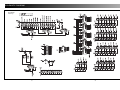
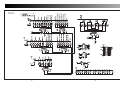
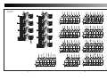
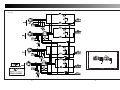
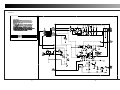
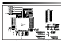
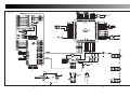
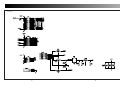
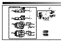
SCHEMATIC DIAGRAM
GEQ - 1231D
FRONT B D
33
34
GEQ - 2231D
FRONT B D 1/2
35
36
GEQ - 2231D
FRONT B D 2/2
37
38
IN/OUT B D
39
40
POWER B D
41
42
SHT B D 1/4
43
44
SHT B D 2/4
45
46
SHT B D 3/4
47
48
SHT B D 4/4
49
50
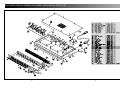
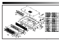
EXPLODED CIEW OF CABINET & CHASSIS / MACHANICAL PARTS LIST
51
52
53
54
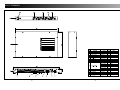
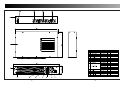
ASS’Y DRAWING
55
56
57
58
NOTE