1
TK-5710(B)/5710H(B)
CIRCUIT DESCRIPTION
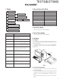
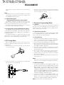
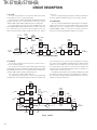
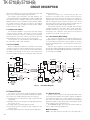
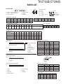
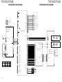
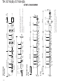
4-5. Final Amplifier Circuit (From Power module to
Antenna output): TK-5710H (B)
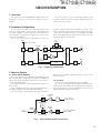
The transmit signal from the TX terminal (CN1) of the final
unit (X45-376) is amplified by the power module (IC1).
The signal amplified by the power module is divided into
two signal, and further is amplified by the final amplifier
(Q1,Q2). The each signal from Q1 and Q2 is combined.
The combined signal passes through the antenna switch
(D6, D8, D9), CM coupler and low-pass filter, then it is fed to
the antenna.
CM coupler is a line for detecting forward wave and
reflected wave.
Forward wave is detected by D3, and is converted into
DC voltage. The converted DC voltage is fed to the APC
comparator (IC2), and is compared with the PC voltage, then
is output from the OUT-B terminal (pin 7) of IC2 as an APC
voltage. The APC voltage controls the gate voltage of the
power module (IC1) and final amplifier (Q1,Q2), and keeps
transmission output stable.
If an abnormal antenna load is connected, reflected wave
is detected by D4, and output voltage (DC voltage) is fed to
the APC comparator (IC2). The transmission output is
reduced more as this DC voltage rises.
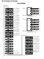
FINAL UNIT (X45-376)
ANT
Final AMP +B
Q1
LPF
CM
COUPLER
+B
Final AMP +B
Q2
IC1
TX(CN1)
D3
POWER
MODULE
FWD
DET
8T
IC2
D4
REFL
DET
VR1
D6
D8,D9
ANT
SW
8T
APC
PC
Fig. 10
Final amplifier circuit: TK-5710H (B)
4-6. Temperature Protection Circuit : TK-5710 (B)
4-7. Temperature Protection Circuit : TK-5710H (B)
To prevent thermal destruction of the power module
(IC2), this circuit reduces APC voltage when temperature of
the power module (IC2) rises.
The CPU (IC703) detects temperature with a thermistor
(TH1) and controls reference voltage to the APC circuit.
To prevent thermal destruction of the power module
(IC1) and final amplifier (Q1,Q2), this circuit reduces APC
voltage when temperature of the power module (IC1) and
final amplifier (Q1,Q2) rises.
The CPU (IC703) detects temperature with the
thermistor (TH1,TH2) and controls reference voltage to the
APC circuit.
5. PLL Frequency Synthesizer
The PLL Frequency Synthesizer consists of the following
components:
• VCXO (X400)
• VCO (Q413, Q414,Q416)
• Rheostat IC (IC401)
• PLL IC (IC400)
• Local switch (D435, D436)
5-1. VCXO (X400)
VCXO (X400) generates a reference frequency of 16.8
MHz for the PLL frequency synthesizer. This reference
frequency is applied to pin 10 of the PLL IC (IC400).
The VCXO oscillation frequency is fine-adjusted by
controlling the voltage applied to pin 1 of the VCXO with DAC
(IC738). It is also controlled with pin 1 of the VCXO if the
output from VCXO is modulated.
5-2. VCO
There is two RX VCOs (RX VCO 1, RX VCO 2) and a TX
VCO.
The RX VCO 1 (Q413) and RX VCO 2 (Q414) generate a 1st
local receive signal. The RX VCO 1 oscillation frequency is
185.95 to 204.9475 MHz and the RX VCO 2 oscillation
frequency is 204.95 to 223.95 MHz.
The TX VCO (Q416) generates a transmit carrier. The TX
VCO oscillation frequency is 136 to 174 MHz.
The VCO oscillation frequency is determined by two
systems of operation switching terminals "STR" and "VCO1/2"
and two systems of voltage control terminals "C/V" and
"ASSIST".
The operation switching terminals, "STR" and "VCO1/2",
are controlled by the control lines (STR, VCO1/2) output from
the CPU (IC703). When the STR logic is high and the VCO1/2
logic is high, the RX VCO 1 output a 1st local receive signal.
When the STR logic is high and the VCO1/2 logic is low, the
29