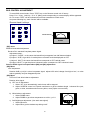
1
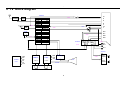
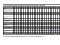
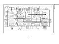
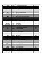
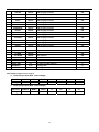
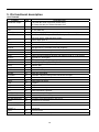
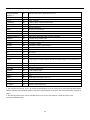
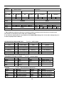
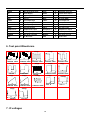
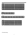
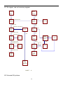
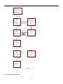
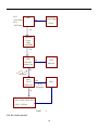
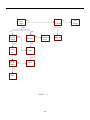
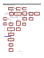
UOC TDA9341(9351)-2NAG SERIES
(PCB:CY-2529PD VER 1.0)
SERVICE MANUAL
COLOUR TELEVISION
.
CONTENTS
1. safety precautions………………………………………………………………………………………3
2.
block diagram
and PHILIPS UOC functional difference between the various IC versions ………………….4
3. Replacement of memory IC……………………………………………………………………………7
4. Service adjustment……………………………………………………………………………………...7
5. ICs functional description………………………………………………………………………………11
6. Test point waveform………………………………………………………………………………….…15
7. All ICs/transistors voltages…………………………………………………………………………….16
8. Purity / convergence adjustment……………………………………………………………………..17
2
.
SAFETY PRECAUTIONS
1.
The design of this product contains special hardware, many
circuits and components specially for safety purposes. For
continued protection, no changes should be made to the
original design unless authorized in writing by the
manufacturer. Replacement parts must be identical to those
used in the original circuits. Service should be performed by
qualified personnel only.
2.
Alterations of the design or circuitry of the products should
not be made. Any design alterations or additions will void
the manufacturer’s warranty and will further relieve the
manufacturer of responsibility for personal injury or property
damage resulting therefrom.
3.
Many electrical and mechanical parts in the products have
special safety-related characteristics. These characteristics
are often not evident from visual inspection nor can the
protection afforded by them necessarily be obtained by
using replacement components rated for higher voltage,
wattage, etc. Replacement parts which have these special
safety characteristics are identified in the parts list of
Service manual. Electrical components having such
features are identified by shading on the schematics
and by ( ! ) on the parts list in Service manual. The use
of a substitute replacement which does not have the same
safety characteristics as the recommended replacement
part shown in the parts list of Service manual may cause
shock, fire, or other hazards
4.
Don’t short between the LIVE side ground and
ISOLATED (NEUTRAL) side ground or EARTH side
ground when repairing. Some model’s power circuit is
partly different in the GND. The difference of the GND is
shown by the LIVE: ( ) side GND, ISOLATED (NEUTRAL) :
( ) side GND and EARTH : (
) side GND. Don’t short
between the LIVE side GND and ISOLATED (NEUTRAL)
side GND or EARTH side GND and never measure with a
measuring apparatus (oscilloscope etc.) the LIVE side GND
and ISOLATED (NEUTRAL) side GND or EARTH side GND
at the same time. If above note will not be kept, a fuse or
any parts will be broken.
5.
If any repair has been made to the chassis, it is
recommended that the B1 setting should be checked or
adjusted (See ADJUSTMENT OF B1 POWER SUPPLY).
6.
The high voltage applied to the picture tube must conform
with that specified in Service manual. Excessive high
voltage can cause an increase in X-Ray emission, arcing
and possible component damage, therefore operation under
excessive high voltage conditions should be kept to a
minimum, or should be prevented. If severe arcing occurs,
remove the AC power immediately and determine the cause
by visual inspection (incorrect installation, cracked or melted
high voltage harness, poor soldering, etc.). To maintain the
proper minimum level of soft X-Ray emission, components
in the high voltage circuitry including the picture tube must
be the exact replacements or alternatives approved by the
manufacturer of the complete product.
7.
Do not check high voltage by drawing an arc. Use a high
voltage meter or a high voltage probe with a VTVM.
Discharge the picture tube before attempting meter
connection, by connecting a clip lead to the ground frame
and connecting the other end of the lead through a 10kΩ
2W resitor to the anode button.
8.
When service is required, observe the original lead dress.
Extra precaution should be given to assure correct lead
dress in the high voltage circuit area. Where a short circuit
has occurred, those components that indicate evidence of
overheating should be replaced. Always use the
manufacturer’s replacement components.
9.
10. Isolation Check
(Safety for Electrical Shock Hazard)
After re-assembling the product, always perform an isolation
check on the exposed metal parts of the cabinet (antenna
terminals, video/audio input and output terminals, Control
knobs, metal cabinet, screwheads, earphone jack, control
shafts, etc.) to be sure the product is safe to operate without
danger of electrical shock.
11. The surface of the TV screen is coated with a thin film which
can easily be damaged. Be very careful with it when handle
the TV. Should the TV screen become soiled, wipe it with a
soft dry cloth. Never rub it forcefully. Never use any cleaner
or detergent on it.
(1)
(2)
3
Dielectric Strength Test
The isolation between the AC primary circuit and all metal
parts exposed to the user, particularly any exposed metal
part having a return path to the chassis should withstand a
voltage of 3000V AC (r.m.s.) for a period of one second.
(…Withstand a voltage of 1100V AC (r.m.s.) to an appliance
rated up to 120V, and 3000V AC (r.m.s.) to an appliance
rated 200V or more, for a periode of one second.)
This method of test requires a test equipment not generally
found in the service trade.
Leakage Current Check
Plug the AC line cord directly into the AC outlet (do not use
a line isolation transformer during this check.). Using a
“Leakage Current Tester”, measure the leakage current
from each exposed metal part of the cabinet, particularly
any exposed metal part having a return path to the chassis,
to a known good earth ground (water pipe, etc.). Any
leakage current must not exceed 0.5mA AC (r.m.s.).
However, in tropical area, this must not exceed 0.2mA AC
(r.m.s.).
●Alternate Check Method
Plug the AC line cord directly into the AC outlet ( do not use
a line isolation transformer during this check.). Use an AC
voltmeter having 1000 ohms per volt or more sensitivity in
the following manner. Connect a 1500 Ω 10W resistor
paralleled by a 0.15 μ F AC-type capacitor between an
exposed metal part and a known good earth ground (water
pipe, etc.). Measure the AC voltage across the resistor with
the AC voltmeter. Move the resistor connection to each
exposed metal part, particularly any exposed metal part
having a return path to the chassis, and measure the AC
voltage across the resistor. Now, reverse the plug in the AC
outlet and repeat each measurement. Any voltage
measured must not exceed 0.75V AC (r.m.s.). This
corresponds to 0.5mA AC (r.m.s.).
However, in tropical area, this must not exceed 0.3V AC
(r.m.s.).
This corresponds to 0.2mA AC (r.m.s.)
.
2 TV Block diagram
TDA93XX
TUNER
SAW
S
TRAP
video
Vo
video
IF IN
R IN
RF AGC
GIN
G
B IN
B
C
R
CVBSINT
video
CHROMA
IFVO OUT
CVBS/Y IN
V1i
Y
4052
video
ARo
24C08
ALo
audio
SDA
SCL
ARi2
ARi1
AUDIO OUT
V OUT
IK
RGB OUT
H OUT
TDA9859
A OUTR
A OUTL
MAIN L
MAIN R
SDA/SCL
AV2 R
AV2 R
M OUTR
M OUTL
AV1 L
AV2 L
bus
audio
video
V2i
ALi2
ALi1
audio
AN17821
V IN
H IN
24V
TDA8177
H OUT
16V
8V
V OUT
H OUT
130V
POWER
UNIT
200V
CRT PCB
audio
+15V
-15V
SCREEN
CRT
FOCUS
5V
3.3V
DY
4
Vi1
OUT1OUT1+
Vi2
OUT2OUT2+
.
PHILIPS UOC FUNCTIONAL DIFFERENCE BETWEEN THE VARIOUS IC VERSIONS
IC VERSION
9350 9351 9352 9353 9360 9361 9362 9363 9364 9365 9366 9367 9380 9341 9382 9383 9384 9385 9386 9387 9388 9389 9370 9373 9375 9377 9378
TV rang
90
90
Mono inter-carrier multi-standard
√
Audio switch
Automatic volume leveling
90
110 90
90
110
110
√
√
√
√
√
√
√
√
√
√
√
√
√
√
√
110
110
90
90
90
90
√
√
√
90
110
110
√
√
√
√
√
√
√
110
110
90
110
√
√
√
√
110
90
110
√
√
√
√
110
90
110
√
√
√
√
√
√
Sound demodulator (4.5-6.5MHz)
With switch able centre frequency
√
√
Automatic volume leveling or
√
√
√
√
√
√
√
√
√
√
√
√
√
√
√
√
√
√
√
√
√
√
Subcarrier output (for comb filter
applications)
√
QSS sound IF amplifier with
√
√
√
√
√
Separate input and AGC circuit
√
AM sound demodulator without
√
Extra reference circuit
PAL decoder
√
SECAM decoder
NTSC decoder
√
√
√
√
√
√
√
√
√
√
√
√
√
√
√
√
√
√
√
√
√
√
√
√
√
√
√
√
√
√
√
√
√
√
√
√
√
√
√
√
√
√
√
√
√
√
√
√
√
√
√
√
√
√
√
√
√
√
√
Horizontal geometry(E-W)
√
√
√
√
√
√
√
√
√
√
√
√
√
√
Horizontal and vertical zoom
√
√
√
√
√
√
√
√
√
√
√
√
√
√
64-
64-
64-
64-
64-
16-
16-
16-
16-
16-
16-
16-
32-
32-
32-
32-
64k 64k 64k 64k 128 128 128
128
128
128
128 128 64k 64k 64k 64k
64k
64k
64k
64k 64k
64k
55k 55k
55k
55k 55k
User RAM size
1k
1k
1k
1k
2k
2k
2k
2k
2k
Teletext
1p
1p
1p
1p
10p 10p 10p 10p 10p 10p 10p 10p
Closed captioning
√
√
√
√
√
ROM size
32-
32-
32-
32-
64-
642k
√
2k
√
√
√
√
642k
√
√
16-
16-
16-
1k
1k
1k
1k
1k
1k
1k
1k
1k
1k
2.25 2.25 2.25 2.25 2.25
√
√
√
√
√
√
√
√
√
√
√
Block diagram TDA93xX PS/N2 series with mono intercarrier sound demodulator
5
32-
√
√
√
√
.
6
3.REPLACEMENT OF MEMORY IC
1. MEMORY IC.
This TV uses memory IC. In the memory IC are memorized data for correctly operating the video and
deflection circuits.
When replacing memory IC, be sure to use IC written with the initial value of data.
2. PROCEDURE FOR REPLACING MEMORY IC
(1) Power off
Switch the power off and unplug the power cord from AC outlet.
(2) Replace IC
Be sure to use memory IC written with the initial data values.
(3) Power On
Plug the power cord into the AC outlet and switch the power On.
(4) Check and set SYSTEM default value:
1) Press “QV” key holding about 4 second and then press “MENU1” key on the Remote control unit.
Or Press “TEST” key on the Remote control unit for factory used.
2) The “TEST” will be displayed on the screen.
3) Press digital key, (Mkey) and corresponding on-screen display will be appeared.
Some time “PASSWORD” on-screen display will be appeared, you need to input 828.
4) Check the setting value of the SYSTEM default value of Table below. If the value is different,
select items by [CH+]/[CH-] keys and set value by [VOL+]/[VOL-] keys.
5) Press “STANDBY” key again and return to the normal screen.
4.SERVICE ADJUSTMENT
B1 POWER SUPPLY
1. Receive normal colour bar signal.
2. Connect DC voltmeter to VD541- and isolated ground.
3. Adjust potentiometer in power unit to get the voltage as 110V ±1.0V for 21 inch hereinafter,
130 ±1.0V for 25 inch upwards.
FOCUS ADJUSTMENT
1. Receive a crosshatch signal.
2. While watching the screen, adjust the FOCUS VR to make the vertical and horizontal lines as fine and
sharp as possible.
7
BUS CONTROL ADJUSTMENT
To enter BUS control mode, Press “TEST” key on the Remote control unit of factory.
Press “0” to “4“ key, lock key +“5” to “9” (Mkey) and corresponding on-screen display will be appeared.
On TV screen “TEST” will be indicated, this means entered bus control mode.
And press following key, each function will be available.
Remote Hand Unit keys
[M1]
[M2]
[M3]
c
d
e
f
i
g
j
[M0]
b
h
k
Horizontal line
Shado
[M1] menu
MENU0 Geometrical adjustment
Receive PAL standard Complete pattern signal.
Adjustment steps:
a) Adjust V. SLOPE, to the center horizontal line just appeare from half bottom shadow.
b) Adjust V. SIZE, to get 90% of vertical picture contents would be displayed on CRT.
c) Adjust V. SHIFT, the center horizontal line correspond to CRT vertical center.
d) Adjust H.SHIFT, to get the picture horizontal center correspond to CRT horizontal center.
Receive NTSC signal and repeat above [M0] and [M1] adjustment.
[M2] Menu
AGC Adjustment.
Receive 60dBμ(1mV)VH colour bar pattern signal,adjust AGC value(voltage from high to low),to noise
reduce gradually and just disappeared point.
[M3] Menu
CRTcut off and white balance adjustment.
Receive white signal.
a) CRT cut off adjustment.
1. Select “SC”, then automatically vertical scan will be stopped.
2. Adjust SCREEN control on Flyback transformer to get the darkest single horizontal line (red,
green, or blue, sometimes shows more yellow, more purple or more white).
b) White balance adjustment.
1. Select RD/BD menu.
2. Adjust RD/BD to get colour temperature as x=281, y=311
c) Sub-Brightness adjustment. (Use stair case signal)
1. Select SB menu.
2. Adjust SB to get the darkest step being cutoff.
a
8
I2C standard UOC for export bus control adjustment item default setting
2006-10-12
MI
Items
Variable
M0
SUB CONTRAST
63
Sub contrast
63
SUB COLOUR
63
Sub colour
63
SUB SHARPNESS
63
Sub sharpness
63
SUB TINT
63
Sub tint
32
BASE TINT
63
BASE TINT
32
VOL POINT
M1
M2
1/25/50/75
Preset
recommendation
The1~4th point of S - curve
VOL VALUE
0~99
The volue of VALUE
20/40/60/80
V. SLOPE
35
Picture vertical center adjustment
V. SHIFT
20
Vertical positions adjustment
V. SIZE
25
Vertical amplitude adjustment
V. SC
18
Vertical s-correction adjustment
H. SHIFT
15
Horizontal position adjustment
PROGRAM NO.
0
AGC
0~63
AGC take over
26
SEARCH SPEED
0~3
Search speed
0
SHIPPING
M3
BT
0~100
brightness
50
CT
0~100
contrast
75
SC
M4
M5
Screen line
RB
0~63
R bais adjusted
32
GB
0~63
G bais adjusted
32
RD
0~63
R drive adjusted
32
GD
0~63
G drive adjusted
32
BD
0~63
B drive adjusted
32
SB
0~63
Sub brightness
45
OSD V.POS
0~28
Vertical position of OSD
15
OSD H.POS
0~63
Horizital position of OSD
40
OSD GR
0~15
OSD brightness
2
CATHODE
0~15
CATHODE voltage adjust
4
PP mode
PP mode select( standard / dynamic / mild/PIC WB)
standard
Brightness
0~100
Brightness in pp mode
50
Contrast
0~100
Contrast in pp mode
75
Color
0~100
Color in pp mode
50
Sharpness
0~100
Sharpness in pp mode
75
Sc brightness
0~63
Brightness of screen line
45
9
M6
M7
M8
YD PAL
0~15
Y-delay adjustment for PAL signal
8
YD NTSC
0~15
Y-delay adjustment for NTSC signal
8
YD SECAM
0~15
Y-delay adjustment for SECAM signal
8
YD AV PAL
0~15
Y-delay adjustment for PAL signal in AV mode
8
RGB HS+
0~15
RBG hor. offset
8
OSO
0/1
Switch –off in vertical over scan
1
AGC SPEED
0~3
AGC speed
3
FFI
0/1
Fast filter IF -PLL
0
FSL
0/1
Forced slicing level for vertical sync
0
FMWS
0/1
Widow selection of narrow-band sound PLL
0
RPO
0/3
Ratio pre_overshoot
2
NTSC Matrix
USA
NTSC matrix selection
1
Vol pin
0~!
VOL PIN selection (Open drain)
0
UOC VOL
0~1
The volume control of internal UOC
0
FM ATT
0~63
Fm att gain
45
SOFT CLIP
0~3
Soft clip adjust
2
PEAK WHITE
0~15
Peak white adjust
4
CORING
0~3
Coring adjust
1
IF
Vision IF of RF (38/38.9/45.75058.75)
38.9
D/K
ON/OFF
Sound system(6.5MHZ)
ON
I
ON/OFF
Sound system(6.0MHZ)
ON
B/G
ON/OFF
Sound system(5.5MHZ)
ON
M
ON/OFF
Sound system(4.5MHZ)
OFF
SIF PRI
B/G/DK/I/M
Force sound system as auto search
B/G
AUTO SOUND
ON/OFF
Auto sound system as auto search
ON
A V2
ON/OFF
AV2 selection
ON
SVHS
ON/OFF
SVHS seletion
ON
EURO
ON/OFF
Scart input seletio
ON
YUV
ON/OFF
YUV seletion
OFF
PIN 5
4.5M/RGB
Function selection(NTSC/RGB)
RGB
VIDEO OUT
CVBS/IF
Selected video out (pin38)
CVBS
FRENCH
ON/OFF
OSD language selection
ON
RUSSIAN
ON/OFF
OSD language selection
ON
TURKISH
ON/OFF
OSD language selection
ON
FARSI
ON/OFF
OSD language selection
ON
ARABIC
ON/OFF
OSD language selection
ON
BULGARIAN
ON/OFF
OSD language selection
ON
RUMANIAN
ON/OFF
OSD language selection
ON
SPANISH
ON/OFF
OSD language selection
ON
PORTUGUESE
ON/OFF
OSD language selection
ON
10
M9
ITALIAN
ON/OFF
OSD language selection
ON
KEY BOARD
0/1
GERMAN
ON/OFF
OSD language selection
ON
DUTH
ON/OFF
OSD language selection
ON
SWEDISH
ON/OFF
OSD language selection
ON
NORWEGIAN
ON/OFF
OSD language selection
ON
HUNGARIAN
ON/OFF
OSD language selection
ON
POLISH
ON/OFF
OSD language selection
ON
CZECH
ON/OFF
OSD language selection
ON
SLOVENE
ON/OFF
OSD language selection
ON
CROATIAN
ON/OFF
OSD language selection
ON
MACEDONIAN
ON/OFF
OSD language selection
ON
SERBIAN
ON/OFF
OSD language selection
ON
GREEK
ON/OFF
OSD language selection
ON
LOGO
ON/OFF
Logo selection
OFF
AV MEM
ON/OFF
16:9 MODE
ON/OFF
16:9 selection
ON
GAME
ON/OFF
GAME selection
ON
CALENDAR
ON/OFF
CALENDAR selection
ON
START ON
0/1
ON DELAY
ON DELAY M
1
ON
AC power on start selection
0
0~15
On delay time
0
5~15
Factory On delay time
5
KEY BOARD: multiple-choice test(0/1)
0: Control keys input (Max. Limit voltage)
Function
POWER
MENU
TV/AV
V-
V+
P-
P+
Voltage
0
0.4125
0.825
1.2375
1.65
2.0625
2.475
1: Control keys input (Max. Limit voltage)
Function
Voltage
POWER
MENU
TV/AV
V-
V+
P-
P+
2.2
1.75
0.85
1.3
0.4
0.0
11
5. ICs functional description
UOC TDA93XX
SYMBOL
PIN
DESCRIPTION
STAND BY output.
1
In STAND BY mode, high level (Power OFF).
For Power ON this pin will be reduced to low.
SCL
2
I2C-bus clock line
SDA
3
I2C-bus data line
TUNING
4
tuning Voltage (Vt) PWM output
P3.0/NTSC SW
5
Port 3.0 or NTSC output/SCART SW input, Forced NTSC selection,
Low-level output, otherwise High output.
KEY
6
Control keys input *3
VOL
7
Sound Volume control PWM output
MUTE
8
Sound mute output
VSSC/P
9
Digit ground for μ-controller core and periphery
BAND1
10
Tuner Band selection output
BAND2
11
Tuner Band selection output
VSSA
12
Analog ground of teletext decoder and digital ground of TV-processor
SECPLL
13
SECAM PLL decoupling
VP2
14
2nd supply voltage TV-processor(+8V)
DECDIG
15
decoupling digital supply of TV-processor
PH2LF
16
Phase-2 filter
PH1LF
17
Phase-1 filter
GND3
18
Ground 3 for TV-processor
DECBG
19
Band gap decoupling
AVL/EWD
20
Automatic volume leveling /EAST-WEST drive output
VDRB
21
Vertical drive B output
VDRA
22
Vertical drive A output
IFIN1
23
IF input 1
IFIN2
24
IF input 2
IREF
25
Reference current input
VSC
26
Vertical sawtooth capacitor
TUNER AGC
27
Tuner AGC output
AUDEEM/SIFIN1 *1
28
Audio deemphasis or SIF input
DECSDEM/SIFIN2
29
decoupling sound demodulator or SIF input 2
GND2
30
ground 2 for TV processor
SNDPLL/SIFAGC *1
31
narrow band PLL filter or AGC sound IF
AVL/SNDIF/REF0/
AMOUT *1
32
Automatic Volume Levelling / sound IF input / subcarrier reference output / audio
HOUT
33
horizontal output
FBISO
34
flyback input/sandcastle output
deemphasis
12
AUDEXT/QSSO/
AMOUT *1
35
external audio output / QSS intercarrier out
EHTO
36
EHT/overvoltage protection input
PLL IF
37
IF-PLL loop filter
IFVO/SVO
38
IF video output / selected CVBS output
VP1
39
supply voltage TV processor
CVBS INT
40
internal CVBS input
GND1
41
ground for TV processor
CVBS/Y
42
CVBS/Y input
CHROMA
43
C input
AUDOUT/AMOUT *1
44
audio output /AM audio output (volume controlled)
INSSW2
45
2nd RGB / YUV insertion input
R2/VIN
46
2nd R input / V (R-Y) input / PR input
G2/YIN
47
2nd G input / Y input
B2/UIN
48
2nd B input / U (B-Y) input / PB input
BCLIN
49
beam current limiter input
BLKIN
50
black current input / V-guard input
RO
51
Red output
GO
52
Green output
BO
53
Blue output
VDDA
54
analog supply of Closed Caption decoder and digital supply of TV-processor (3.3
V)
VPE
55
OTP Programming Voltage
VDDC
56
digital supply to core (3.3 V)
OSCGND
57
oscillator ground supply
XTALIN
58
crystal oscillator input
XTALOUT
59
crystal oscillator output
RESET
60
reset
VDDP
61
digital supply to periphery (+3.3 V)
P1.0/INT1
62
TV/AV (AV1) / AV2 /S-VHS mode Output.
P1.1/T0
63
TV/AV (AV1) / AV2 /S-VHS mode Output.
P1.2/INT0
64
Remote control signal input.
Note
1. The function of pin 20, 28, 29, 31, 32, 35 and 44 is dependent on the IC version (mono intercarrier FM demodulator
/QSS IF amplifier and East-West output or not) and on some software control bits. The valid combinations are given in
table 1.
2. the vertical guard function can be controlled via pin 49 or pin 50. the selection is made by means of the
IVG bit in subaddress 2BH.
13
TABLE 1
IC version
FM-PLL version
East-West
QSS version
N
Y
N
Y
Y/N
CMB1/CMB0
00
01/10/11
00
01/10/11
00
-
-
-
-
-
01/10/11
00
01/10/11
bits
AM bits
AVL
Pin 20
0
EWD
1
-
AVL
AUDEEM
SIFIN1
Pin 29
DECSDEM
SIFIN2
Pin 31
SNDPLL
SIFAGC
SNDIF(1)
REFO(2)
AVL/SNDIF(1)
Pin 35
AUDEXT
Pin 44
AUDOUT
REFO(2)
1
EWD
Pin 28
Pin 32
0
AMOUT
REFO(2)
AUDEXT
QSSO
AMOUT
AMOUT
REFO(2)
AUDEXT
QSSO
AMOUT
Controlled AM or audio out
Note
1. When additional (external) selectivity is required for FM-PLL system pin 32 can be used as sound IF input.
This function is selected by means of SIF bit in subaddress 28H.
2. the reference output signal is only available for the CMB1/CMB0 setting of 0/1. for the other settings this pin is
a switch output(see also 5 table 67).
AN7522/AN17821/AN7523/AN17823
Function : audio output
Symbol
PIN
Function
Symbol
PIN
Function
Vcc
1
Power supply
GND
7
ground
Out 1 (+)
2
Ch 1 output (+)
In 2
8
Ch 2 input
GND(out 1)
3
Ch 1Ground
VOL
9
Volume Control
Out 1 (-)
4
Ch 1 output (-)
Out 2 (-)
10
Ch 2 output (-)
Standby
5
Mute input
GND(out 2)
11
Ch 2 Ground
In 1
6
Ch 1 input
Out 2 (+)
12
Ch 2 output (+)
Note: AN7523 is pin 1 to 9, AN7522 is pin 1 to 12.
LA9302A/8177/LA78041/LA78040
Function : vertical output
Symbol
PIN
Function
Symbol
PIN
Function
INV IN
1
Input
V OUT
5
Vertical output
VCC1
2
Power
VCC2
6
Output power supply
PUMP UP
3
Pump up power
NON INV IN
7
Negative feedback
GND
4
Ground
TDA9859
Symbol
Function : Universal Sound processor
Pin
Function
Symbol
Pin
Function
AV1L
1
AV1 Audio Left input
AV1R
32
AV1 Audio input Right
P1
2
Not used
P2
31
Not used
MAINL
3
Main Audio Left input
AV2R
30
AV2 Audio input Right
CSMO
4
Smoothing Capacitor
CPS1
29
Pseudo stereo Cap. 1
14
MAINR
5
Main Audio Right input
AV2L
28
AV2 Audio input Left
VP
6
Power Supply
CPS2
27
Pseudo stereo Cap. 2
OUT R
7
Right Output
OUT L
26
Left Output
GND
8
Ground
MAD
25
Not used (GND)
LINOR
9
Line Output Right
LINOL
24
Line Output Left
LINIR
10
Line Input Right
LINIL
23
Line Input Left
CBR1
11
Bass Cap. Right 1
CBL1
22
Bass Cap. Left 1
CBR2
12
Bass Cap. Right 2
CBL2
21
Bass Cap. Left 2
Headphone R
13
Headphone-R output
Headphone L
20
Headphone-L output
CTR
14
Treble Cap. Right
CTL
19
Treble Cap. Left
MAINOR
15
Main Audio out Right
MAINOL
18
Main Audio out Left
SCL
16
I2C Bus clock
SDA
17
I2C Bus data
6. Test point Waveforms
1.2Vpp
2.6Vpp
H
TDA93XX PIN38
H
TDA93XX PIN40
95Vpp
H
95Vpp
CRT KR
H
CRT KG
1Vpp
0.8Vpp
V
V
TDA93XX PIN21
TDA93XX PIN22
22Vpp
300Vpp
H
HEATER
H
T511 PIN7
3.8Vpp
2.5Vpp
H
TDA93XX PIN53
H
TDA93XX PIN52
95Vpp
0.9Vpp
H
CRT KB
1.3Vpp
H
TDA93XX PIN33
2.7Vpp
H
V451 B
TDA93XX PIN59
7. IC voltages
15
2.5Vpp
H
TDA93XX PIN51
5Vpp
H
TDA93XX PIN34
1000Vpp
H
V451 C
TDA93XX
PIN
1
2
3
4
5
6
7
8
9
10
11
12
13
14
15
16
V
2.8
3.8
3.6
3.3
3.5
3.5
0.1
0.1
0
5.4
0.1
0
2.3
8
5
3
PIN
17
18
19
20
21
22
23
24
25
26
27
28
29
30
31
32
V
4
0
4
0.9
0.7
0.8
1.9
1.9
3.9
3.8
1.6
3.2
3.4
0
2.4
0.1
PIN
33
34
35
36
37
38
39
40
41
42
43
44
45
46
47
48
V
0.6
0.5
3.7
1.7
2.4
3.1
8
3.8
0
3.4
1.5
3.6
2.3
2.6
2.6
2.6
PIN
49
50
51
52
53
54
55
56
57
58
59
60
61
62
63
64
V
2.3
7.2
2.7
2.7
2.7
3.5
0
3.5
0.1
1.7
1.8
0
3.5
0.1
0.1
5
TDA8177
PIN
1
2
3
4
5
6
7
V
0.7
15
-12
-15
0.3
15.9
-0.07
AN 7522
PIN
1
2
3
4
5
6
7
8
9
10
11
12
V
12
7
0
7
3.3
1.4
0
1.4
0
7
0
7
TDA9859
PIN
1
2
3
4
5
6
7
8
9
10
11
12
13
14
V
4.0
0
4.0
8.0
4.0
8.0
4.0
0
4.0
4.0
4.0
4.0
4.0
4.0
PIN
15
16
17
18
19
20
21
22
23
24
25
26
27
28
V
4.0
4.5
4.6
4.0
4.0
4.0
4.0
4.0
4.0
4.0
0
4.0
4.0
4.0
PIN
29
30
31
32
V
4.0
4.0
0
4.0
8 Trouble shorting
16
8.1 No signai, can not receive program.
Antenna
Button
Input
Function
Yes
Power off
Noise-Normal
No
Tuning
Blue BG.
R558 etc.
Voltage
Noise-Fad
Yes
33V
Interfere on Screen-No
Check
N201
Pin 23,24
VL
VH
Voltage
C105
Interference-Yes
No
Yes
Yes
Interference-No
Check
Z101
Input
N201
No
Pin10,Pin11
Voltage
Auto
Z101
Search
Interference-Yes
Signa
Yes
Interference No
Check
V101
Base
N201
Pin-38
Signa
V101
And
Sorround
Yes
Interference Yes
V202
V201
Z201 etc.
A101
And
Surroun
N201
And
Sorround
CHART
A
8.2 Unusual AV picture.
17
5Vp-p(H)
No
A101
N201
AV/S-VHS/YUV
Signal Input
Yes
N802
Pin9,10
Voltag
No
Re Table*
N201
Pin63 or 62
Voltag
Yes
N201
No
Yes
N201
Pin42 Signal
1.1Vp-p(H)
No
C806
Yes
N802
Input Signal
No
AV Input
Circuit
Yes
N802 etc.
CHART
B
8.3 One horizontal line.
18
Pin 2
N301
+14V Power
No
Power Supply
Pin 4
Circuit
-16V Power
Yes
Deflection
Circuit
R394
C304 etc.
Yes
N201
Pin 21/22
Wave Form
C231
No
N201 etc.
Yes
1.8Vp-p(V)
N301
Pin 1/7
Wave Form
Yes
N301
0.6Vp-p(V)
No
R301、R303、R218、R217
C301、C303 etc.
CHART
C
8.4 No audio sound.
19
N201
Pin 44
Signa
N601
Yes
Pin1Powe
No
TV
12V
Yes
AV
N201
Pin 44
Signal
Yes
N201
35Signal
No
N801
Switching
Circuit
Yes
No
C210
N201
etc.
Yes
N201
Pin 28
Signa
Yes
Yes
C213
No
N201
CHART
D
20
N601 etc.
No
12V
Power
8.5 No picture and sound.
Power Supply
Output Voltage
No
No
V451
R561etc
Collector Vol.
115V
Yes
N201
Stand-by V451 Base Electrode No
No
Pin33
Wave Form
Wave Form
Normal?
No
Yes
C507
Voltage
Yes
Yes
Yes
300V
R402 etc
Yes
Heater
Ye
8V
Yes
0.8V(H)
Yes
No
R502 etc
N201
Pin 39
Voltage
D506
R511
Yes
R510
D512、D511
Voltage
Yes
CRT
No
T401 etc.
Yes
R504、R503
D508
Yes
T501
Secondary Load
Yes
V501
V502 etc.
Yes
T501 etc
CHART
E
21
N201
No
+8V
Power Supply
8. PURITY / CONVERGENCE ADJUSTMENT
PURITY ADJUSTMENT
WEDGE
1.
Demagnetize CRT with the demagnetizer.
2.
Loosen the retainer screw of the deflection yoke.
3.
Remove the wedges.
4.
Input a green raster signal from the signal generator,
and turn the screen to green raster.
DEFLECTION YOKE
P
CRT
5.
Move the deflection yoke backward.
6.
Bring the long lug of the purity magnets on the short
lug and position them horizontally. (Fig2)
4 6
P/C MAGNETS
7.
Adjust the gap between two lugs so that the GREEN
RASTER will come into the center of the screen.
(Fig. 3)
8.
Move the deflection yoke forward, and fix the position
of the deflection yoke so that the whole screen will
become green.
9.
Insert the wedge to the top side of the deflection
yoke so that it will not move.
P: PURITY MAGNET
4: 4-POLES (convergence magnets)
6: 6-POLES (convergence magnets)
Fig. 1
PURITY MAGNETS
Long lug
10. Imput a crosshatch signal.
11. Verify that the screen is horizontal.
12. Input red and blue raster signals, and make sure that
purity is properly adjusted.
Short lug
Bring the long lug over the short lug
and position them horizontally.
Fig. 2
(FRONT VIEW)
GREEN RASTER
CENTER
Fig. 3
22
STATIC CONVERGENCE ADJUSTMENT
1. Input a crosshatch signal.
2. Using 4-pole convergence magnets, overlap the red
and blue lines in the center of the screen (Fig. 1) and
turn them to magenta (red/blue).
3. Using 6-pole convergence magnets, overlap the
magenta (red/blue) and green lines in the center of the
screen and turn them to white.
(FRONT VIEW)
4. Repeat 2 and 3 above, and make the best
convergence.
Fig. 1
(FRONT VIEW)
DYNAMIC CONVERGENCE ADJUSTMENT
RED
1. Move the deflection yoke up and down and overlap
lines in the periphery. (Fig. 2)
2. Move the deflection yoke left to right and overlap the
lines in the periphery. (Fig. 3)
3. Repeat 1 and 2 above, and make the best
convergence.
GREEN BLUE
BLUE
RED
GREEN
GREEN
RED
BLUE
BLUE GREEN RED
Fig.2
(FRONT VIEW)
After adjustment, fix the wedge at the original position.
Fasten the retainer screw of the deflection yoke.
Fix the 6 magnets with glue.
RED GREEN BLUE
BLUE GREEN RED
RED
GREEN
BLUE
BLUE
GREEN
RED
Fig. 3
23