1
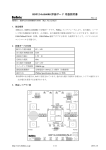
CPU Evaluation Board Instruction Manual
CPU 評価ボード 取 扱 説 明 書
SERIES
2
はじめに
このたびは、BBF2004 シリーズをお買い上げ頂き、誠にありがとうございます。
本製品は、富士通株式会社製 16 ビットマイクロコントローラ F2MC-16LX ファミリ、32 ビットマイクロコントローラ FR ファミリの
MCU を使用したシステムの開発を支援する装置です。
ご使用になる前に本取り扱い説明書をよくお読み下さい。また、後日のために必ず保存しておいて下さい。
目次
はじめに───────────────────────────────── 2
目次─────────────────────────────────── 2
注意─────────────────────────────────── 3
重要事項───────────────────────────────── 3
本ボード使用時の注意事項───────────────────────── 4
1. 概要─────────────────────────────────── 5
1.1特徴───────────────────────────────── 5
1.2構成品──────────────────────────────── 5
2. 本ボードをお使いになる前に──────────────────────── 6
3. 本ボードの機能────────────────────────────── 6
3.1機能一覧─────────────────────────────── 6
4. 本ボードの使用方法 ──────────────────────────── 7
4.1動作電圧設定───────────────────────────── 8
4.2クロック設定───────────────────────────── 8
4.3リセットスイッチおよびハードウェアスタンバイスイッチ───────── 8
4.4評価用 LED ───────────────────────────── 8
4.5A/D コンバータ────────────────────────────9
4.6各種信号確認端子─────────────────────────── 9
4.7I/O ポート外部出力端子 ──────────────────────── 9
4.8シリアル書き込み ───────────────────────────9
4.9CAN 通信 ────────────────────────────── 9
4.10 LIN 通信 ────────────────────────────── 9
5. 接続方法 ────────────────────────────────10
5.1メインボードとドータボードの接続 ────────────────── 10
5.2専用エミュレータ (ICE) と評価ボードの接続 ────────────── 10
5.3シリアルライタと評価ボードの接続 ────────────────── 10
5.4電源ケーブルの接続 ───────────────────────── 10
問い合わせ先一覧 ──────────────────────────── 11
3
注意
本製品をご使用になる前に、必ず本取り扱い説明書をよく読み理解して下さい。誤った使用方法や接続方法は、本製品およびユーザープロ
グラムの破壊につながります。
本ボードは富士通株式会社製 16 ビットマイクロコントローラ F2MC-16LX ファミリ、32 ビットマイクロコントローラ FR ファミリ
MCU(以降、MCU と略す)のフラッシュメモリ内蔵 MCU の書き替えもサポートしております。
本取り扱い説明書中の "XXX" は、本ボード上のシルク文字を表します。
重要事項
本ボードをご使用になる前に、本取り扱い説明書をよく読んで理解して下さい。本取り扱い説明書は必ず保管し、ご使用になっているとき
や不明な点がある場合は、再度よく読み返して下さい。
本ボードとは:
本ボードとは、サンハヤト株式会社(以降、当社と略す)が製作したつぎの製品です。
(1)BBF2004 メインボード(以降、メインボードと略す) 型名:BBF2004-MB
(2)BBF2004 ドータボード(以降、ドータボードと略す) 型名:BBF2004- *** -NB
お客様のホストコンピュータ、専用エミュレータ (ICE)、シリアルライタおよびケーブル類は含みません。
本ボードの使用目的:
本ボードは、富士通株式会社製 16 ビットマイクロコントローラ F2MC-16LX ファミリ、32 ビットマイクロコントローラ FR ファミリの
MCU を使用したシステムの開発を支援する装置です。
この使用目的に従って、本ボードを正しくお使い下さい。この使用目的以外のご使用を堅くお断り致します。
使用制限:
本ボードは、開発支援を目的として製作したものです。機器組み込み用として使用しないで下さい。また、つぎに示す開発用途に対しても
使用しないで下さい。
(1)人命にかかわる装置、医療機器用
(2)原子力開発機器用
(3)航空機器開発用
(4)宇宙開発機器用
このような目的で本ボードの採用を検討されるお客様は、事前に当社研究開発本部へご連絡頂きますようお願い致します。
製品の変更について:
製品の改良のため、デザイン・仕様・取り扱い説明書の内容等を予告なく変更することがあります。
その他の重要事項:
1. 本取り扱い説明書に記載された情報、製品および回路の使用において起因する損害、または特許権やその他の権利の侵害に関しては、当
社は一切その責任を負いません。
2. 本取り扱い説明書によって、第三者または当社の特許権やその他権利の実施権を許諾するものではありません。
版権所有:
本取り扱い説明書および本ボードは著作権で保護されており、全ての権利は当社に帰属しております。本取り扱い説明書の一部や全てのい
かなる箇所も、事前に当社の書面による許諾なしに、複写、複製、転載することはできません。
図について:
本取り扱い説明書の図の一部は、実物と違っていることがあります。
そのときは、本取り扱い説明書に記載されている設定方法に合わせて、お手元のボード設定および動作評価を行って下さい。
予測できる危険の限界:
当社では、潜在的な危険が存在するおそれのある全ての起こり得る諸状況や誤使用を予測できません。したがって、本取り扱い説明書と本
ボードに添付されている警告が全てではありません。お客様の責任で、本ボードを正しく安全にお使い下さい。
安全事項:
1. 本ボードをお使いになる前に、必ず本取り扱い説明書をお読みになり理解して下さい。
2. 本取り扱い説明書は、必ず保管し、ご使用になっているときや不明な点がある場合は、再読して下さい。
4
重要事項
シグナル・ワードの定義:
これは、安全警告記号です。潜在的に、人に危害を与える危険に対し注意を喚起するために用います。
起こり得る危害または死を回避するためにこの記号の後に続く全ての安全メッセージに従ってください。
危険
「危険」は、回避しないと死亡事故または重傷を招く差し迫った危険な状況を示します。ただし、本製品
警告
「警告」は、回避しないと死亡または重症を招く可能性がある潜在的に危険な状況を示します。
注意
「注意」は、回避しないと軽傷または中程度の傷害を招くことがある潜在的に危険な状況を示します。
注 意
では該当するものはありません。
安全記号のつかない注意は、回避しないと財物損傷を引き起こすことがある潜在的に危険な状況を示し
ます。
注意事項、留意事項は、例外的な条件や注意を操作手順や説明記述の中でお客様に伝達する場合に使用しています。
警告
(1)感電、火災等の危険防止および品質保証のために、お客様ご自身による修理や改造は行わないで下さい。
(2)ホストコンピュータ、本ボードおよび周辺デバッグ装置の電源を入れた状態で、全てのケーブル類およびジャンパースイッチ用コ
ネクタの脱着を行わないで下さい。電源を入れた状態で脱着を行った場合は、ホストコンピュータ、本ボードおよび周辺デバッグ
装置の破壊または発煙、発火の可能性があります。また、評価中のユーザープログラムを破壊する可能性があります。
(3)本ボードの電源を入れた状態で、IC ソケットに対して MCU の脱着を行わないで下さい。電源を入れた状態で MCU の脱着を行っ
た場合は、ホストコンピュータ、本ボード、周辺デバッグ装置および MCU の破壊または発煙、発火の可能性があります。また、
評価中のユーザープログラムを破壊する可能性があります。
(4)電源供給については電源仕様に従って供給して下さい。仕様以外の電源電圧を加えないで下さい。
本ボード使用時の注意事項
本ボード使用時の注意事項に記載されている事項は、本ボードを使用する上で全ての場合に該当し、例外は存在しません。したがって、
本ボードをご使用になる前につぎに示す警告文をよく読み、完全に理解して下さい。
ただし、ここに記載されている事項は本ボードの使用時における共通の警告のみが記載されており、これが本ボードを使用する上での全
ての警告ではありません。
警告
ホストコンピュータ、本ボードおよび周辺デバッグ装置の電源を入れた状態で、全てのケーブル類、ジャンパースイッチ用コネクタおよび
MCU の脱着を行わないで下さい。電源を入れた状態で脱着を行った場合は、ホストコンピュータ、本ボード、MCU および周辺デバッグ
装置の破壊または発煙、発火の可能性があります。また、評価中のユーザープログラムを破壊する可能性があります。
注 意
ホストコンピュータ、本ボードおよび周辺デバッグ装置の位置関係により、本ボードのインターフェース部に大きなストレスが加わり、
接点の機械的破損や接触不良等を招く場合があります。また、使用中に周辺デバッグ装置や本ボードを動かすと、インターフェース部
に思わぬストレスを与えることになります。設置位置に十分ご注意下さい。
5
1. 概要
本ボードは、富士通株式会社製 16 ビットマイクロコントローラ F2MC-16LX ファミリ、32 ビットマイクロコントローラ FR ファミリの
MCU を、お客様のシステムに組み込む前の簡易的な動作評価を行うことが可能なため、お客様の開発効率の向上に貢献します。
本ボードは、メインボードとドーターボードの構成となっています。専用エミュレータ (ICE) を使用したデバッグを行うことや、フラッシ
ュメモリ内蔵 MCU の評価およびシリアル書き込み用ライタとして使用することができます。メインボードは各品種共通で、ドーターボー
ドを変更することで各品種に対応できます。シリアル書き込みの詳細については、富士通株式会社へお問い合わせ下さい。
1.1 特徴
本ボードの特徴をつぎに示します。
(1)外部入力電源電圧は DC 7V 〜 10V に対応しています。ジャンパースイッチの切り替えにより MCU の動作電圧 3V、5V 両方に対
応します。
(2)MCU のピン全てに対して信号チェックピンがあるので、各入出力ポートの信号の確認だけでなく、クロックや電源・グランド等の測
定が簡単にできます。
(3)P00 〜 P07 の入出力ポートに対して LED 点灯機能があります。お客様が動作チェック用回路基板を用意することなく、簡単なプ
ログラムの動作確認や使用デバイスの比較評価がすぐにできます。
(4)メインボード上の可変抵抗を使用することにより、アナログ入力端子 (MCU 信号名 AN0) に対して入力値の変更が簡単にできます。
(5)I/O ポート外部出力端子があります。
(6)シリアル接続をしてプログラム書き込みを行うことで、MCU をユーザーターゲットシステムへ実装できます。なお、シリアル書き込
みには、富士通標準シリアルオンボード書き込みをサポートしています。詳しくは富士通株式会社へお問い合わせ下さい。
1.2 構成品
本ボードの構成品を図1−1、表1−1に示します。梱包を開けましたら、表1−1に記載されている構成品がきちんと揃っているかご確
認下さい。
BBF2004 メインボード
BBF2004 ドータボード
(図は BBF2004-64CL-NB)
図1−1 BBF2004 1 評価ボード構成図
No.
1
2
品 名
BBF2004 評価ボード
メインボード 型番:BBF2004-MB
BBF2004 評価ボード
ドータボード 型番:BBF2004- *** -NB
3
ジャンパースイッチ用コネクタ
4
電源ケーブル用プラグ
数 量
備 考
1
1
ご使用になる MCU により型番が異なります。
11+α ご購入の製品により数量が異なります。
1
・BBF2004 SERIES 取扱説明書
5
・メインボード回路図
・ドータボード個別取扱説明書
1
・ドータボード回路図
表1−1 構成品
ドータボードの個別取扱説明書および回路図はご購入の
ドータボードにより異なります。
6
2. 本ボードをお使いになる前に
注 意
本ボードをお使いになる前に、つぎに示す注意事項を必ずよくお読みになり、理解して下さい。誤ってご使用になりますと、ホストコ
ンピュータ、本ボード、MCU、周辺デバッグ装置およびユーザープログラムの破壊につながります。メインボード上のレギュレータ
"IC3" は、MCU の種類、MCU の動作および評価環境の温度により熱くなることがありますので注意して下さい。
(1) 本ボードを使用するときは、スペーサーを取り外さないで下さい。
(2) 本ボードに重量物を上積みするなど、無理な力や応力を加えないで下さい。
(3) 本ボードに過大な物理的衝撃や力を与えないで下さい。
(4) 指定された電圧以外の電源を供給しないで下さい。
(5) 設置場所を移動する場合は、本ボードに強い振動、衝撃が加わらないように注意して下さい。
(6) ジャンパースイッチ用コネクタ(以降、コネクタと略す)、ディップスイッチを設定するときは、本ボードおよび周辺デバッグ装置の
電源を必ずお切り下さい。
(7) コネクタの接続位置およびディップスイッチの ON にする番号をよく確認の上、正しく設定して下さい。正しく設定されていないと、
MCU、本ボードおよびユーザープログラムを破壊する可能性があります。
(8) 設定に使用しないコネクタは、全て取り外して下さい。動作確認の際、不具合発生の原因になります。
(9) 全てのケーブルの接続を終えてから、各装置の電源を投入して下さい。
(10) 本ボード単体でのエミュレーションはできません。専用エミュレータ(ICE)を接続してエミュレーションを行って下さい。専用エミュレータ
(ICE) については富士通株式会社へお問い合わせ下さい。
(11) 本ボードを使用して MCU の評価を行う場合は、MCU の1番ピンの位置に注意して IC を搭載して下さい。
(12) 本ボードを簡易ライタとして使用し、連続で複数の MCU に書き込みを行う場合は、MCU 脱着時、本ボードの電源を必ずお切り下さい。
(13)MCU の書き替え回数には制限があります。
(14) 本ボードを使用して、評価を行った MCU を機器組み込み用として使用しないで下さい。 評価を行った MCU にはブレークポイント
等の設定で MCU の書き替えを行っていますのでストレスがかかっ ています。
3. 本ボードの機能
3.1 機能一覧
本ボードの機能一覧を表3−1に示します。
No.
項 目
仕 様
MCU の動作評価
各 MCU に対応したドータボードと使用することにより MCU の動作評価が可能です。
2
ジャンパースイッチ設定
MCU の動作環境の設定を行います。
3
ディップスイッチ設定
MCU の動作環境の設定を行います。
4
MCU へ対しての外部リセット、
ハードウェアスタンバイモード設定
MCU に対するリセット信号の入力、ハードウェアスタンバイモードの設定が可能です。
5
電源確認用 LED
MCU への電源供給時に LED( 赤色 ) が点灯します。
6
評価用 LED
1
LED( 緑色 ) による出力ポート P00 〜 P07 の動作確認が可能です。
メインクロック、サブクロックが搭載可能です。
(本ボードに発振子とコンデンサは付属していません)
7
クロック設定
8
A/D コンバータ入力設定
AN0 へ可変電圧を入力可能です。
9
MCU 動作電圧設定
MCU に合わせて 3V または 5 Vの設定が可能です。
表3−1 機能一覧
7
4. 本ボードの使用方法
本ボードは、ご使用になる MCU に対応したドータボードとメインボードを組み合わせて使用します。専用エミュレータ (ICE) を使用した
デバッグを行うときや MCU をドータボード上の IC ソケットに搭載し動作させるときは、それぞれの使用方法に合った設定を本ボード上
で設定して下さい。本ボードの設定方法は、本取り扱い説明書の各項をご覧下さい。メインボートには、リセットスイッチ、MCU の各種
機能設定スイッチ、評価用 LED、評価用可変抵抗、信号確認用端子、I/O ポート外部出力端子、シリアル通信用コネクタがあります。また、
GND 端子 5 ヶ所、VCC 端子 4 ヶ所を用意してありますのでオシロスコープ等の測定時、MCU 信号のプルアップ、プルダウン時等の作
業性がよくなっています。ドータボードには、LIN 通信評価用端子、CAN 通信評価用コネクタ、MCU 端子切り替え用ジャンパースイッチ
があります。(ドータボードの種類によって、搭載機能が異なります)
図4−1に各スイッチ等の位置を示します。表4−1にスイッチの機能を示します。
BBF2004 メインボード
図4−1 各部の配置
No.
スイッチ種類
1
ジャンパースイッチ
2
3
4
機 能
SW3No.
MCU の各信号の切り換え用。同梱
されているコネクタにて切り換え。
SW3:MCU 動作モード設定用。使用
する MCU の動作環境に合わせて設定。
1:MD0
6:AN0
2:MD1
7:SIN
メインボード上の
3:MD2
8:SOT
ディップスイッチ
4:AVRH
9:PX0
5:AVRL
10:PX1
上記名称は、MCU の信号名に対応。
(PX0、PX1 を除く)
外部リセット
スイッチ
MCU に対しリセット信号の入力。
ボタンを押すと GND 電位を発生。
MCU のハードウェアスタンバイモー
ハードウェア
ドの設定。
スタンバイスイッチ
ボタンを押すと GND 電位を発生。
機 能
出荷時設定
1
MD0 設定用(ON: 'H'、OFF: 'L' )
OFF
2
MD1 設定用(ON: 'H'、OFF: 'L' )
OFF
3
MD2 設定用(ON: 'H'、OFF: 'L' )
OFF
4
AVRH 設定用(ON: 'H'、OFF:L 未接続)
ON
5
AVRL 設定用(ON: 'L'、OFF:L 未接続)
ON
6
AN0 設定用(ON:0V 〜 VCC、
OFF:L 未接続)
OFF
7
SIN YDC/PC ライタ切替用(ON:PC ライタ
使用時、OFF:YDC ライタ使用時)
OFF
8
SOT YDC/PC ライタ切替用(ON:PC ライ
タ使用時、OFF:YDC ライタ使用時)
OFF
9
書き込みプログラム起動端子 PX0 設定用
(ON: 'H'、OFF: 'L' )※
OFF
10
書き込みプログラム起動端子 PX1 設定用
(ON: 'H'、OFF: 'L' )※
OFF
表4−1 各スイッチ機能
表4−2 ディップスイッチ SW3 各種機能
※ PX0、PX1 は、MCU の書き込みプログラム起動端子のポートです。
書き込みプログラム起動端子が P00, P01 の場合、P00=PX0、P01=PX1 となります。
8
4. 本ボードの使用方法
4.1 動作電圧設定
メインボードには、MCU および周辺機能の動作電圧の切り替えを行うため、ジャンパースイ
ッチ "V-IN" があります。ご使用になる MCU および周辺機能に合わせて "V-IN" を 3V または
5V のどちらかに設定して下さい。 "V-IN" が開放状態のときは、MCU および周辺機能へ電源
は供給されません。電源が供給され 3V または 5V の電圧を発生したとき、電源確認用 LED
"VCC" が点灯します。
図4−2 動作電圧 3V 設定時
メインボードへの電源供給の方法については、5.4項を参照して下さい。
4.2 クロック設定
メインボードには、MCU に対してメインクロック "MAIN" とサブクロック "SUB" を入力す
るためのソケットがあります。ソケットはそれぞれ、クロック発生用の発振子をセットする
ソケットと、コンデンサをセットするソケットがあります。お客様のご使用にあわせて対応
図4−3 動作電圧 5V 設定時
発振子とコンデンサをご用意して頂き、ソケットにセットして下さい。
メインクロック "MAIN"(MCU の X0,X1 へ接続されます)
X1:発振子をセットするソケットです。
XC1、XC2:コンデンサ用ソケットです。
2 ピン ,3 ピンタイプのどちらの種類でもセットすることができます。
1 番と 3 番または 2 番と 3 番へセットして下さい。
図4−4 メインクロック用ソケット部
サブクロック "SUB"(MCU の X0A,X1A へ接続されます)
X1A:発振子をセットするソケットです。
2 ピン ,3 ピンタイプのどちらの種類でもセットすることができます。
XCA1、XCA2:コンデンサ用ソケットです。
1 番と 3 番または 2 番と 3 番へセットして下さい。
4.3 リセットスイッチおよびハードウェアスタンバイスイッチ
メインボードには、MCU へリセット入力するための、リセットスイッチ "RESET" およびハ
図4−5 サブクロック用ソケット部
ードウェアスタンバイスイッチ "HSTX" があります。
図4−6にリセットスイッチ部の回路図を示します。
4.4 評価用 LED
メインボードには、動作確認のための LED があります。LED は、対応ポートの出力が 'H' の
ときに点灯します。点灯させる MCU のポートに対応したジャンパースイッチをコネクタで
接続して下さい。コネクタで接続することにより、MCU の I/O ポートと LED が接続されます。
表4−3に LED に対応する MCU の I/O ポートおよびジャンパースイッチを示します。
※ドータボード BBF2001-100QF2-NB および BBF2001-100CL2-NB 使用時、LED P06 と P07 は点灯しません。下記ジャンパ接続することにより点灯可能です。
図4−6 リセットスイッチおよび
ハードハードウェアスイッチ部回路図
LED P06:信号確認端子 CP2 の 101 番ピンと LED 接続用ジャンパースイッチ JP6(LED
側のピン)を接続。
LED P07:信号確認端子 CP2 の 102 番ピンと LED 接続用ジャンパースイッチ JP7(LED
側のピン)を接続。
LED
対応 MCU I/O ポート
対応ジャンパースイッチ
P00
P00
JP0
P01
P01
JP1
P02
P02
JP2
P03
P03
JP3
P04
P04
JP4
P05
P05
JP5
P06
P06
JP6
P07
P07
JP7
表4−3 LED、MCU I/O ポート、ジャンパースイッチ対応表
図4−7
9
4. 本ボードの使用方法
4.5 A/D コンバータ
本ボードには MCU の A/D コンバータに関して下記の機能があります。
(1)A/D コンバータの電源 AVCC、AVSS は、AVCC = VCC、AVSS = GND に固定されています。
(2)A/D コンバータ用基準電圧 AVRH、AVRL はメインボード上のディップスイッチ "SW3" の 4 番、
5 番で設定可能です。
AVRH :
AVRL :
SW3 の 4 番
MCU AVRH 端子の状態
SW3 の 5 番
MCU AVRL 端子の状態
ON
VCC へ接続
ON
GND へ接続
OFF
未接続
OFF
未接続
図4−8 AVRH、AVRL 出荷時設定
出荷時設 SW3.4:ON(AVRH = VCC)、SW3.5:ON(AVRL = GND)
(3)アナログ入力端子 AN0 に対して、メインボード上のディップスイ
ッチ”SW3”の 6 番を ON にすることにより任意の電圧を入力可
能です。(図4−9参照)
入力電圧値は GND から VCC までです。入力電圧値の設定はメイ
ンボード上の可変抵抗 "AN0" で設定します。(図4−10参照)
出荷時設定:AN0 = GND
図4−9
図4−10
4.6 各種信号確認端子
メインボードには MCU のピン全てに対して信号確認のためのピン CP1,CP2,CP3,CP4 があります。シルク表記されている番号は、
MCU のピン番号に対応します。MCU の信号状態をオシロスコープ等の測定機、またユーザーインターフェース接続が可能です。
4.7 I/O ポート外部出力端子
メインボードには、I/O ポートの信号を外部へ取り出すためのスルーホ
ール(2x32 グリッド 2.54mm ピッチ φ 1.0 TH 仕上げ)を設けてあ
ります。必要に応じてコネクタを半田付けして使用することも可能です。
対 象 I/O ポ ー ト は P00 〜 P07、P10 〜 P17、P20 〜 P27、P30
〜 P37、P40 〜 P47、P50 〜 P57、P60 〜 P67、P70 〜 P77 です。
図4−11
4.8 シリアル書き込み
本ボードと富士通製 PC シリアルライタ(以降、PC ライタと略す)または、横河ディジタルコンピュータ製シリアルライタ(以降、YDC
ライタと略す)を使用し、オンボードでフラッシュメモリ内蔵 MCU にシリアル書き込みができます。
シリアル書き込みについての詳細は、ドータボード個別の取り扱い説明書をご覧下さい。
本ボードとシリアルライタの接続方法については本取り扱い説明書 5.3項の「シリアルライタと評価ボードの接続」をご覧下さい。
4.9 CAN 通信
ドータボードの種類によって CAN 通信の評価ができます。CAN 対応のドータボードで CAN 通信評価を行う場合は、ドータボード個別の
取り扱い説明書をご覧下さい。
4.10 LIN 通信
ドータボードの種類によって LIN 通信の評価ができます。LIN 対応のドータボードで LIN 通信評価を行う場合は、ドータボード個別の取
り扱い説明書をご覧下さい。
10
5. 接続方法
警告
接続を行う前には、ホストコンピュータ、本ボードおよび全ての周辺デバッグ装置の電源は必ずお切り下さい。電源が入ったまま接続
すると、ホストコンピュータ、本ボードおよび周辺デバッグ装置の破壊または発煙、発火の可能性があります。
5.1 メインボードとドータボードの接続
メインボードとドータボードの接続は、メインボード上のコネクター CN1、CN2、CN3、CN4 と、ドータボー
ド裏面のコネクター CN1、CN2、CN3、CN4 の面取りされている位置を合わせてしっかりと接続して下さい。
5.2 専用エミュレータ (ICE) と評価ボードの接続
専用エミュレータ(ICE)との接続は ICE プローブを使用して接続します。ICE プローブの先端形状についての詳
しい内容は富士通株式会社へお問い合わせ下さい。
図5−1
また、接続方法の詳細については専用エミュレータ (ICE) の説明書をご覧下さい。
5.3 シリアルライタと評価ボードの接続
警告
本ボードへケーブルの接続を行うときは、本ボード、周辺デバッグ機器の電源を必ずお切り下さい。電源が入ったままでケーブルの接
続を行うと本ボードや周辺デバッグ装置の破壊または発煙、発火の可能性があります。
メインボードにはシリアルライタ接続ケーブル用のコネクタが設けられております。コネクタの
向きに注意して接続して下さい。なお、PC ライタについては富士通株式会社へ、YDC ライタに
ついては横河ディジタルコンピュータ株式会社へお問い合わせ下さい。
5.3.1 PC ライタをご使用の場合
RS232C ケーブル(D-SUB 9 ピン ストレートタイプ)は、メインボード上の D-SUB
コネクタ "PC WRITER(RS232C)" へ接続して下さい。
RS232C ドライバ "IC1" は、メインボードに搭載しております。
5.3.2 YDC ライタをご使用の場合
シリアルライタに合わせて専用ケーブルをメインボード上のコネクタ "YDC WRITER" へ
接続して下さい。
図5−2
5.4 電源ケーブルの接続
警告
(1)電源ケーブルは VCC、GND の接続を間違えないように十分注意して下さい。VCC と GND が正常に接続されない場合は、本ボ
ードや周辺デバッグ装置の破壊または発煙、発火の可能性があります。
(2)許容電源電圧範囲外の電源供給はしないで下さい。許容電源電圧範囲外の電源供給をした場合、本ボードや周辺デバッグ装置の破
壊または発煙、発火の可能性があります。
メインボードへの外部入力電源電圧は、DC7V 〜 10V に対応しています。本製品に付属のプラグをご使用になりメインボード上の DC ジ
ャック "JC1" へ電源の入力を行って下さい。
許容電源電圧範囲
消費電流
7V 〜 10V(DC)
100 〜 300mA
表5−1 電源動作範囲
※消費電流は、デバイスの種類、使用方法により変わります。
図5−3 プラグ内部回路
11
5. 接続方法
動作電圧チェックピン(メインボード上の "EXT VCC","EXT VSS" 端子)から直接電源(定電圧電源)を供給することも可能です。動作
電圧チェックピンには、MCU および周辺機能に合わせて 3V または 5V を直接入力して下さい。 3V または 5V の電源が供給されたとき
に電源確認用 LED "VCC" が点灯します。
直接電源を供給する際は、メインボード上のジャンパースイッチ "V-IN" を必ずオープンにして下さい。ジャンパースイッチ "V-IN" を 3V
または 5V 側へコネクタで接続されている場合は、本ボード、周辺デバッグ装置の破壊または、発煙、発火の可能性があります。
また "EXT VCC"(VCC 端子)、"EXT GND"(VSS 端子)を間違えないよう十分に注意して接続して下さい。VCC と GND が正常に接続
されない場合は、本ボード、周辺デバッグ装置の破壊または、発煙、発火の可能性があります。
図5−4
お問い合わせ先一覧
サンハヤト株式会社
研究開発本部
〒 170-0005 東京都豊島区南大塚 3-40-1
電話:03-5951-4821(直通)
FAX:03-5985-7667
E-mail: [email protected]
富士通マイクロエレクトロニクス株式会社
システムマイクロ事業部 ソリューション技術部
〒 211-8588 神奈川県川崎市中原区上小田中 4-1-1
電話:044-754-2128
FAX:044-754-2714
横河ディジタルコンピュータ株式会社
機器事業部 サポートセンタ
〒 183-8540 東京都府中市府中町 1-9 京王府中 1 丁目ビル
電話:042-333-6245
FAX:042-352-6107
13
CPU Evaluation Board
INSTRUCTION MANUAL
SERIES
Preface
Thank you very much for purchasing the BBF2004 Series products.
This product is a device that assists in developing systems by using MCU of the 16-bit microcontroller, F 2MC-16LX Family or 32-bit
microcontroller, FR Family of Fujitsu.
Read this manual carefully before using this product. Keep the manual for use in future.
Contents
Preface────────────────────────────────────────────── 13
Contents───────────────────────────────────────────── 13
Notes─────────────────────────────────────────────── 14
Important Items───────────────────────────────────────── 14
Notes When Using this Board ──────────────────────────────── 15
1. Outline ────────────────────────────────────────────── 16
1.1 Features ────────────────────────────────────────── 16
1.2 Components──────────────────────────────────────── 16
2. Before Using this Board──────────────────────────────────── 17
3. Functions of this Board ──────────────────────────────────── 17
3.1 List of Functions ───────────────────────────────────── 17
4. Usage of this Board ────────────────────────────────────── 18
4.1 Operating Voltage Setting ─────────────────────────────── 18
4.2 Clock Setting ─────────────────────────────────────── 19
4.3 Reset Switch and Hardware Standby Switch──────────────────── 19
4.4 Evaluation LEDs ───────────────────────────────────── 19
4.5 A/D Converter─────────────────────────────────────── 20
4.6 Signal Confirmation Pins ──────────────────────────────── 20
4.7 I/O Port External Output Pin ────────────────────────────── 20
4.8 Serial Writing ─────────────────────────────────────── 20
4.9 CAN Communication ────────────────────────────────── 20
4.10 LIN Communication ─────────────────────────────────── 20
5. Connection Methods────────────────────────────────────── 20
5.1 Connection of Main Board and Daughter Boards ───────────────── 20
5.2 Connection of Dedicated Emulator (ICE) and Evaluation Board ────────
5.3 Connection of Serial Writer and Evaluation Board───────────────── 21
5.4 Connection of Power Cable ────────────────────────────── 21
List of Contact windows
21
14
Notes
Before using this product, be sure to read this manual carefully and understand its contents. Using it inappropriately or connecting it incorrectly
could lead to damage of this product and any user program. This board also supports rewriting of the Flash memory built-in MCU of the 16-bit
microcontroller F2MC-16LX Family or 32-bit microcontroller FR Family MCU (hereinafter called MCU) of Fujitsu. "xxx" in this manual indicates
the silk-screening characters on this board.
Important Items
Before using this board, read this instruction manual carefully and understand its contents. Keep this instruction manual and, when you
encounter a problem while using this board, read it again.
What is this board?
This board is one of the following products manufactured by Sunhayato Corporation (hereinafter called the company).
(1) BBF2004 main board (hereinafter called the main board) Type No.: BBF2004-MB
(2) BBF2004 daughter board (hereinafter called the daughter board) Type No.: BBF2004-***-NB
The customer's host computer, dedicated emulator (ICE), serial writer, and cables are not included.
Application of this board
This board supports the development of a system by using MCU of the 16-bit microcontroller, F2MC-16LX Family or 32-bit microcontroller,
FR Family of Fujitsu. Use this board correctly for this purpose. Do not use this board for other purposes.
Constraints
This board is manufactured to support the development. Do not use it as the built-in board for a device. Also do not use it for the following
development purposes.
(1) For life-related and medical devices
(2) For nuclear power development devices
(3) For aircraft device development
(4) For space development devices
Any customer who considers the use of this board for any of the above purposes should contact Research and Development Div. of the
company in advance.
Change in product
To improve the product, its design and specifications, and the contents of the instruction manual may be revised without prior notice.
Other important notes
1. Our company takes no responsibility whatsoever for any damage resulting from the use of information, products, and circuits contained in
this manual or infringements of patent and other rights.
2. This manual does neither grant the permission of patent nor other rights of any third party or our company.
Copyrights
This manual and the board are protected by copyrights and they all belong to our company. No part or any location in this manual may be
reproduced or reprinted without prior written permission from our company.
Figures
Part of the figures in this manual may be different from the real product.
In such a case, make a setting for this board and evaluate its operation by adjusting the setting methods described in this manual.
Limitations of predictable risks
Our company cannot predict all circumstances and incorrect usages that could lead to potential danger. Therefore, warnings included in this
manual and the board do not necessarily cover all dangerous situations. Use this board safely on customer's own responsibility.
Safety
1. Before using this board, read this manual and understand its contents.
2. Keep this manual and read it again when using this product or there is any question concerning it.
15
Important Items
Signal/word definitions
This is a safety warning mark. This mark is used to draw user's attention to potential danger to human
being. To avoid possible injury or death, be sure to observe all safety messages following this mark.
Danger
"Danger" indicates that death or serious injury will occur if imminent danger is not avoided.However, this
Warning
"Warning" indicates that death or serious injury could occur if potential danger is not avoided.
Caution
"Caution" indicates that minor or moderate injury may occur if potentialdanger is not avoided.
Caution
does not apply to this product.
"Caution" without a safety warning mark indicates that property damagmay occur if potential danger is not
avoided.
Notes and Precautions are used to inform the customer of exceptional conditions or notes in the operation procedures and descriptions of
the manual.
Warning
(1) Do not repair and modify this board in order to prevent danger such as electric shocks and fire and also to assure the quality of the board.
(2) Do not disconnect and connect any cable and/or jumper switch connector while the host computer, this board, and/or any peripheral debug device is turned on. If a cable or jumper switch connector is disconnected or connected while the host computer, this board, or
any peripheral debug device is turned on, the host computer, this board, and/or a peripheral debug device could be damaged, or smoking or fire could be caused. Also, any user program under evaluation could be damaged.
(3) Do not disconnect the MCU from the IC socket and connect the MCU to the IC socket while his board is turned on. If the MCU is disconnected or connected while this board is turned on, the host computer, this board, a peripheral debug device, and/or MCU could be damaged, or smoking or fire could be caused. Also, any user program under evaluation could be damaged.
(4) Supply power according to the power supply specifications. Do not apply any voltage out of the specifications.
Notes When Using this Board
'Notes When Using This Board' apply to all cases in which this board is used and no exception exists. Thus, before using this board, read
the following warning messages carefully and understand them. However, only common warnings when using this board are described here
and thus they do not necessarily include all warnings when using this board.
Warning
Do not disconnect and connect any cable, jumper switch connector, and/or MCU while the host computer, this board, and/or any peripheral debug device
is turned on. If a cable, jumper switch connector, MCU is disconnected or connected while the host computer, this board, or any peripheral debug device
is turned on, the host computer, this board, MCU, and/or a peripheral debug device could be damaged, or smoking or fire could be caused. Also, any user
program under evaluation could be damaged.
Caution
Excessive stress may be applied to the interface of this board depending on the relative positions of the host computer, this board, and peripheral
debug device, leading to mechanical damage or poor connection at contact points. If the peripheral debug device and/or this board is moved while in
use, unexpected stress may be applied to the interface. Thus, it is necessary to pay sufficient attention to the installation locations.
16
1. Outline
This board will contribute to improving development efficiency of the customer because it is possible to perform simple operation evaluation
before embedding MCU of the 16-bit microcontroller, F2MC-16LX Family or 32-bit microcontroller, FR Family of Fujitsu in customer's system.
This board consists of the main board and a daughter board. It can be used to perform debugging by using a dedicated emulator (ICE) and
evaluation of the Flash memory built-in MCU, and also as a writer for serial writing. The main board is common to all types and each type
can be accommodated by changing the daughter board. For details of the serial writing, contact Fujitsu Limited.
1.1 Features
This section shows some of the features of this board
(1) The external input supply voltage of DC 7 V to 10 V is supported. By changing the jumper switch, the operating voltages of both 3 V and 5 V of the MCU are supported.
(2) Since there is a signal confirmation pin to all pins of the MCU, it is possible not only to confirm the signal of each I/O port, but also to measure the clock, power supply, and ground easily.
(3) The LED lighting function is provided for the I/O ports of P00 to P07. The customer can immediately perform simple operation confirmations of programs and evaluation of used devices by comparison without providing a circuit board for operation confirmations.
(4) By using a variable resistor on the main board, the input value of the analog input pin (MCU) signal name: AN0) can be easily changed.
(5) The I/O port external output pin is provided.
(6) By writing a program through serial connection, the MCU can be mounted in the user target system. The Fujitsu standard serial on-board writing is supported for serial writing. For more details, contact Fujitsu Limited.
1.2 Components
Figure 1-1 and Table 1-1 shows the components of this board. After opening the packing, make sure that the components listed in Table 1-1
are contained in the packing.
BBF2004 main board
BBF2004 daughter board
(The figure below shows BBF2004-64CL-NB)
Figure 1-1 BBF2004 evaluation board configuration diagram
No.
1
2
Part name
BBF2004 evaluation board
Main board type: BBF2004-MB
BBF2004 evaluation board
Daughter board type: BBF2004-***-NB
3
Jumper switch connector
4
Power cable plug
Quantity
1
1
11+α
* Main board circuit diagram
* Instruction manual to individual daughter board
This type depends on an MCU to be used.
The quantity depends on the product purchased.
1
* Instruction manual to BBF2004 SERIES
5
Remarks
The instruction manual to individual daughter board
1
and the circuit diagram depend on the daughter board
purchased.
* Daughter board circuit diagram
Table 1-1 Components
17
2. Before Using this Board
Caution
Before using this board, read the notes shown below and understand them. If the board is used incorrectly, the host computer, this
board, MCU, peripheral debug device, and user program may be damaged. Notice that the regulator "IC3" on the main board may
become hot depending on the MCU type, MCU operation, and temperature in the evaluation environment.
(1) Do not remove the spacer while using this board.
(2) Do not apply unreasonable force or stress by, for example, putting something heavy on this board.
(3) Do not apply excessive physical impact or force.
(4) Supply only the specified voltages.
(5) When moving the installation location, care should be taken so that neither strong vibration nor impact is applied to this board.
(6) Before setting the jumper switch connector (hereinafter called the connector) or DIP switches, turn off this board and peripheral debug device.
(7) Make the correct setting after thoroughly checking the connector connection locations and numbers of DIP switch to be turned 'ON.' If the setting is incorrect, MCU, this board, and the user program may be damaged.
(8) Remove all connectors not to be used for the setting. Otherwise, any malfunction could occur when checking the operations.
(9) Turn on each device after connecting all cables.
(10) Emulation of this board alone cannot be performed. Perform the emulation by connecting a dedicated emulator (ICE). For information on the dedicated emulator (ICE), contact Fujitsu Limited.
(11) To evaluate the MCU by using this board, pay attention to the location of 1st pin of the MCU for mounting IC.
(12) When writing continuously to multiple MCUs by using this board as a simple writer, turn off this board before removing or mounting each MCU.
(13) The number of times of rewriting to each MCU is limited.
(14) Do not use an MCU evaluated by using this board to be mounted on equipment because the MCU that was evaluated has been stressed by rewriting to the MCU with the settings of break points, etc.
3. Functions of this Board
3.1 List of Functions
Table 3-1 shows the functions of this board.
No.
Function
Description
1
MCU operation evaluation
MCU operation can be evaluated by using a daughter board
corresponding to each MCU.
2
Jumper switch setting
Sets the operating environment for the MCU.
3
DIP switch setting
Sets the operating environment for the MCU.
4
External reset/hardware standby mode setting to the MCU
Reset signal input/hardware standby mode setting can be
5
Power supply confirmation LED
LED (red) is lit while power is supplied to the MCU.
6
Evaluation LEDs
Operation checks of the output ports, P00 to P07 can be
made by each LED (green).
7
A/D converter input setting
The main clock or sub-clock can be mounted.
(This board does neither include oscillator nor capacitor)
8
Clock setting
Variable voltage to AN0 can be input.
9
MCU operating voltage setting
3 V or 5 V setting can be made corresponding to the MCU.
performed to the MCU.
Table 3-1 List of functions
18
4. Usage of this Board
This board is intended to be used by combining the main board and the daughter board corresponding to the MCU to be used. To perform
debugging by using a dedicated emulator (ICE) or mount the MCU in the IC socket on the daughter board to operate, make a setting
appropriate to each usage of this board. For information on the setting method of this board, see the appropriate sections of this manual.
The main board has its reset switch, various functional setting switches of the MCU, evaluation LEDs, variable resistor for evaluation, signal
confirmation pin, I/O port external output pin, and serial communication connector. Five GND pins and four VCC pins are included to make
measurement by an oscilloscope, etc. and pull-up/pull-down operation of the MCU signal more efficient. The daughter board has its LIN
communication evaluation pin, CAN communication evaluation connector, and MCU pin switching jumper switch (its functions vary on the
type of daughter board). Figure 4-1 shows the location of each switch. Table 4-2 shows the function of each switch.
BBF2004 main board
Figure 4-1 Placement of each part
No. Switch type
1
2
3
4
Jumper
switch
Function
Used to switch the signal of the MCU.The
provided connector is used for switchining.
Used to set the "SW3": MCU operation mode. Set the switch corresponding to the operating
DIP switch environment of the MCU to be used.
2:MD1
3:MD2
4:AVRH 5:AVRL
on the main 1:MD0
board
6:AN0
7:SIN
8:SOT
9:PX0
10:PX1
The above names correspond to the signal names
of MCU. (However, PX0 and PX1 are excluded.)
External
Used to input the reset signal to the MCU. Pressing
reset switch this button generates the ground potential.
Hardware
standby
switch
Used to set the hardware standby mode of the MCU.
Pressing this button generates the ground potential.
Table 4-1 Switch functions
Setting when
shipped
Function
SW3 No.
1
MD0 setting (ON: 'H', OFF: 'L')
OFF
2
MD1 setting (ON: 'H', OFF: 'L')
OFF
3
MD2 setting (ON: 'H', OFF: 'L')
OFF
4
AVRH setting (ON: 'H', OFF: not connected)
ON
5
AVRL setting (ON: 'L', OFF: not connected)
ON
6
AN0 setting (ON: 0V to VCC, OFF: not connected)
OFF
7
SIN YDC/PC writer switching (ON: When PC writer
is used; OFF: When YDC writer is used)
OFF
8
SOT YDC/PC writer switching (ON: When PC writer
is used; OFF: When YDC writer is used)
OFF
9
Writing program activation pin for setting PX0 (ON: 'H', OFF: 'L') *
OFF
10
Writing program activation pin for setting PX1
(ON: 'H', OFF: 'L') *
OFF
Table 4-2 Various functions of DIP switch 'SW3'
* PX0 and PX1 are the writing program activation pin ports of the MCU.
When the writing program activation pins are P00 and P01, the following relationship holds: P00 = PX0 and P01 = PX1.
4.1 Operating Voltage Setting
The jumper switch "V-IN" is provided on the main board to switch
the operating voltage of the MCU and peripheral function devices.
Set "V-IN" to 3 V or 5 V adjusting to the MCU and peripheral
function devices to be used.When "V-IN" is open, no power is
supplied to the MCU and peripheral function devices.When power
is supplied and the voltage of 3 V or 5 V is generated, the power
confirming LED "VCC" is lit. For information on the method to
supply power to the main board, see Item 5.4.
Figure 4-2
Operating voltage set to 3 V
Figure 4-3
Operating voltage set to 5 V
19
4. Usage of this Board
4.2 Clock Setting
On the main board, the socket to supply the main clock "MAIN" and that to supply the sub-clock "SUB"
to the MCU are included. There are two sockets available: one for setting an oscillator to generate
the clock and the other for setting a capacitor. Prepare oscillators and capacitors suitable to the
customer's environment and then set them.
Main clock "MAIN" (connected to X0 and X1 of the MCU)
Figure 4-4 Socket for the main clock
X1: Socket used to set an oscillator
Either the 2-pin or 3-pin type can be set.
XC1, XC2: Socket for a capacitor
Set a capacitor to the 1st and 3rd or the 2nd and 3rd.
Sub-clock "SUB" (connected to X0A and X1A of the MCU)
X1A: Socket used to set an oscillator
Either the 2-pin or 3-pin type can be set.
Figure 4-5 Socket for the sub-clock
XCA1, XCA2: Socket for a capacitor
Set a capacitorto the 1st and 3rd or the 2nd and 3rd.
4.3 Reset Switch and Hardware Standby Switch
On the main board, the reset switch "RESET" to input the reset signal to the MCU and the hardware
standby switch "HSTX" are included. Figure 4-6 shows a circuit diagram of the reset switch.
4.4 Evaluation LEDs
LEDs for confirming the operation are included on the main board. Each LED lights up while the output
of the corresponding port is 'HIGH.' Connect the jumper switch corresponding to the MCU port to be Figure 4-6 Circuit diagram of reset
switch and hardware switch
lit through a connector. By connecting the jumper switch through a connector, the I/O port of the MCU
and an LED are connected.
Table 4-3 shows the I/O port and jumper switches corresponding to the MCU of each LED:
*When use the daughter board Type No. BBF2001-100QF2-NB or BBF2001-100CL2-NB, LED P06
and LED P07 are not light up. By setting of following, LED’s light up.
LED P06: Connect a 101 pin of “CP2” of Signal Confirmation Pins and jumper switch for LED “JP6”
(LED side pin).
LED P07: Connect a 102 pin of “CP2” of Signal Confirmation Pins and jumper switch for LED “JP7”
(LED side pin).
LED
P00
P01
P02
P03
P04
P05
P06
P07
Corresponding MCU I/O port
P00
P01
P02
P03
P04
P05
P06
P07
Corresponding jumper switch
JP0
JP1
JP2
JP3
JP4
JP5
JP6
JP7
Figure 4-7 MCU I/O port
Table 4-3 Correspondence table of LEDs and jumper switch
4.5 A/D Converter
This board provides the following functions concerning the A/D converter of the MCU:
(1) AVCC and AVSS of the A/D converter power supply are fixed as AVCC = VCC and AVSS = GND.
(2) The A/D converter standard voltages AVRH and AVRL can be set by the 4th and 5th of the DIP switch "SW3" on the main board.
AVRH
4th of SW3
MCU AVRH pin status
AVRL
5th of SW3
MCU AVRH pin status
ON
Connected to VCC
ON
Connected to GND
OFF
Not connected
OFF
Not connected
Setting when shipped: SW3.4:ON (AVRH = VCC), SW3.5:ON (AVRL = GND)
Figure 4-8 AVRH and AVRL
settings when shipped
20
4. Usage of this Board
(3) By turning on the 6th of the DIP switch "SW3" on the main board, any
voltage can be input to the analog input pin AN0 (see Figure 4-9).
The input voltage value ranges from the GND level to VCC. The input voltage
value can be set by using the variable resistor "AN0" on the main board (see
Figure 4-10).
Setting when shipped: AN0 = GND
4.6 Signal Confirmation Pins
On the main board, the signal confirmation pins CP1, CP2, CP3, and CP4 are
included for all pins of the MCU. Numbers in silk screen printing correspond
the pin numbers of the MCU.
Figure 4-9
Figure 4-10
The signal status of the MCU can be measured by a measuring instrument
such as an oscilloscope and also the user interface can be connected.
4.7 I/O Port External Output Pin
On the main board, a through hole (2 x 32 grid, 2.54 mm pitch,φ1.0 TH finish)
is provided to redirect the I/O port signal to the outside. The through hole can
also be used by soldering the connector as required. The target I/O ports are:
P00 to P07, P10 to P17, P20 to P27, P30 to P37, P40 to P47, P50 to P57,
P60 to P67, and P70 to P77.
Figure 4-11
4.8 Serial Writing
By using this board and the Fujitsu PC serial writer (hereinafter called the PC writer) or YDC serial writer serial writing to the on-board Flash
memory built-in MCU can be performed. For details of serial writing, see the instruction manual of each daughter board. For information on
the method to connect this board and the serial writer, see Item 5.3, "Connection of Serial Writer and Evaluation Board" of this manual.
4.9 CAN Communication
CAN communication can be evaluated depending on the type of a daughter board. For details of the evaluation of CAN communication with
a CAN supporting daughter board, see the instruction manual of each daughter board.
4.10 LIN Communication
LIN communication can be evaluated depending on the type of a daughter board.
For details of the evaluation of LIN communication with a LIN supporting daughter board, see the instruction manual of each daughter board.
5. Connection Methods
Warning
Be sure to turn off the host computer, this board, and all peripheral debug devices before connecting them. If they are connected after
power-on, the host computer, this board, and a peripheral debug device could be damaged, or smoking or fire could be caused.
5.1 Connection of Main Board and Daughter Boards
Connect the main board and daughter board reliably by aligning the chamfered positions of connectors
CN1, CN2, CN3, and CN4 on the main board with those of connectors CN1, CN2, CN3, and CN4 on
the rear side of the daughter board.
Figure 5-1
21
5. Connection Methods
5.2 Connection of Dedicated Emulator (ICE) and Evaluation Board
Use an ICE probe to connect to the dedicated emulator (ICE). For details of the shape of the ICE probe tip, contact Fujitsu Limited. For
details of the connection method, see the manual of the dedicated emulator (ICE).
5.3 Connection of Serial Writer and Evaluation Board
Warning
Before connecting a cable to this board, be sure to turn off this board and peripheral debug devices. Connecting a cable while this board
or a peripheral debug device is turned on could damage this board and/or a peripheral debug device, or smoking or fire could be caused.
Connectors for the serial writer connection cable are installed on the main board. Notice the connector
direction while connecting. For information on the PC writer, contact Fujitsu Limited. For information
on the YDC writer, contact Yokogawa Digital Computer Corporation.
5.3.1 Usage of PC writer
Connect a RS232C cable (D-SUB 9pin straight type) to the D-SUB connector "PC WRITER (RS232C)" on the main board. The RS232C driver "IC1" is provided on the main board.
5.3.2 Usage of YDC writer
Connect a special cable to the connector "YDC WRITER" on the main board corresponding to the serial writer.
Figure 5-2
5.4 Connection of Power Cable
Warning
(1) Care should be taken when connecting the power cable to VCC and GND so that they are connected correctly. If VCC or GND is not connected correctly, this board and/or a peripheral debug device could be damaged, or smoking or fire could be caused.
(2) Do not supply power beyond the range of allowable supply voltage. If power beyond the range of allowable supply voltage is supplied, this board and/or a peripheral debug device could be damaged, or smoking or fire could be caused.
The external input supply voltage
to the main board should be
Allowable supply voltage
Current consumption
7V~10V(DC)
100~300mA
between DC 7 V and 10 V. Use
Table 5-1 Power operation range
the plug supplied with this product
to supply power to the DC jack
"JC1" on the main board.
Figure 5-3
Plug internal circuit
* The current consumption depends on the device type and the usage.
It is also possible to supply power (constant voltage supply) directly from the operating voltage check pin ("EXT VCC" and "EXT VSS" pins
on the main board). Supply 3 V or 5 V directly to the operating voltage check pin corresponding to the MCU and peripheral functions. When
3 V or 5 V power is supplied, LED "VCC" for power confirmation is lit.
Before supplying power, be sure to make the jumper switch "V-IN" on the
main board open. If the jumper switch "V-IN" is connected to the 3 V or 5 V
side through a connector, this board or a peripheral debug device could be
damaged, or smoking or fire could be caused.
Care should be taken when connecting "EXT VCC" (VCC pin) and "EXT GND"
(VSS pin) correctly so that they are not incorrect. If VCC or GND is connected
incorrectly, this board and/or a peripheral debug device could be damaged, or
smoking or fire could be caused.
Figure 5-4
List of Contact Windows
Research and Development Div.
Sunhayato Corp.
3-40-1, Minami-Otsuka, Toshima-ku, Tokyo, 170-0005, Japan
Phone: +81-3-5951-4821 (direct)
FAX: +81-3-5985-7667
E-mail: [email protected]
Solution Engineering Dept.
Support Center, Instrument Bussiness Div.
System Micro Div.
Yokogawa Digital Computer Corporation
Fujitsu Microelectronics Limited
Keio-Fuchu 1-Chome Building
1-1, Kamikodanaka 4-chome, Nakahara-ku, Kawasaki, Tokyo, 211-8588,
1-9, Fuchu-cho, Fuchu-shi, Tokyo, 183-8540, Japan
Japan
Phone: +81-42-333-6245
Phone: +81-44-754-2181
FAX: +81-42-352-6107
FAX: +81-44-754-2714
2008.5.22 MNL-BBF2004 Rev.1.4