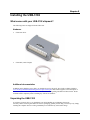
1
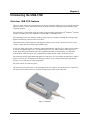
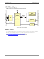
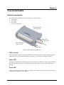
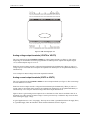
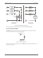
USB-3102 USB-based Analog Output User's Guide Document Revision 4, March, 2009 © Copyright 2009, Measurement Computing Corporation Your new Measurement Computing product comes with a fantastic extra — Management committed to your satisfaction! Thank you for choosing a Measurement Computing product—and congratulations! You own the finest, and you can now enjoy the protection of the most comprehensive warranties and unmatched phone tech support. It’s the embodiment of our mission: To provide PC-based data acquisition hardware and software that will save time and save money. Simple installations minimize the time between setting up your system and actually making measurements. We offer quick and simple access to outstanding live FREE technical support to help integrate MCC products into a DAQ system. Limited Lifetime Warranty: Most MCC products are covered by a limited lifetime warranty against defects in materials or workmanship for the life of the product, to the original purchaser, unless otherwise noted. Any products found to be defective in material or workmanship will be repaired, replaced with same or similar device, or refunded at MCC’s discretion. For specific information, please refer to the terms and conditions of sale. Harsh Environment Program: Any Measurement Computing product that is damaged due to misuse, or any reason, may be eligible for replacement with the same or similar device for 50% of the current list price. I/O boards face some harsh environments, some harsher than the boards are designed to withstand. Contact MCC to determine your product’s eligibility for this program. 30 Day Money-Back Guarantee: Any Measurement Computing Corporation product may be returned within 30 days of purchase for a full refund of the price paid for the product being returned. If you are not satisfied, or chose the wrong product by mistake, you do not have to keep it. These warranties are in lieu of all other warranties, expressed or implied, including any implied warranty of merchantability or fitness for a particular application. The remedies provided herein are the buyer’s sole and exclusive remedies. Neither Measurement Computing Corporation, nor its employees shall be liable for any direct or indirect, special, incidental or consequential damage arising from the use of its products, even if Measurement Computing Corporation has been notified in advance of the possibility of such damages. HM USB-3102.doc 3 Trademark and Copyright Information TracerDAQ, Universal Library, Measurement Computing Corporation, and the Measurement Computing logo are either trademarks or registered trademarks of Measurement Computing Corporation. Windows, Microsoft, and Visual Studio are either trademarks or registered trademarks of Microsoft Corporation LabVIEW is a trademark of National Instruments. CompactFlash is a registered trademark of SanDisk Corporation. XBee and XBee-PRO are trademarks of MaxStream, Inc. All other trademarks are the property of their respective owners. Information furnished by Measurement Computing Corporation is believed to be accurate and reliable. However, no responsibility is assumed by Measurement Computing Corporation neither for its use; nor for any infringements of patents or other rights of third parties, which may result from its use. No license is granted by implication or otherwise under any patent or copyrights of Measurement Computing Corporation. All rights reserved. No part of this publication may be reproduced, stored in a retrieval system, or transmitted, in any form by any means, electronic, mechanical, by photocopying, recording, or otherwise without the prior written permission of Measurement Computing Corporation. Notice Measurement Computing Corporation does not authorize any Measurement Computing Corporation product for use in life support systems and/or devices without prior written consent from Measurement Computing Corporation. Life support devices/systems are devices or systems which, a) are intended for surgical implantation into the body, or b) support or sustain life and whose failure to perform can be reasonably expected to result in injury. Measurement Computing Corporation products are not designed with the components required, and are not subject to the testing required to ensure a level of reliability suitable for the treatment and diagnosis of people. 4 Table of Contents Preface About this User's Guide .......................................................................................................................7 What you will learn from this user's guide ......................................................................................................... 7 Conventions in this user's guide ........................................................................................................................................ 7 Where to find more information ......................................................................................................................... 7 Chapter 1 Introducing the USB-3102 ....................................................................................................................8 Overview: USB-3102 features ............................................................................................................................ 8 USB-3102 block diagram ................................................................................................................................... 9 Software features ................................................................................................................................................ 9 Chapter 2 Installing the USB-3102 ......................................................................................................................10 What comes with your USB-3102 shipment? ................................................................................................... 10 Hardware .........................................................................................................................................................................10 Additional documentation ................................................................................................................................................10 Unpacking the USB-3102 ................................................................................................................................. 10 Installing the software ...................................................................................................................................... 11 Installing the hardware ..................................................................................................................................... 11 Connecting the USB-3102 to your system .......................................................................................................................11 Calibrating the USB-3102 ................................................................................................................................ 12 Chapter 3 Functional Details ...............................................................................................................................13 External components ........................................................................................................................................ 13 USB connector .................................................................................................................................................................13 Status LED .......................................................................................................................................................................13 Power LED ......................................................................................................................................................................13 Screw terminal banks .......................................................................................................................................................14 Analog voltage output terminals (VOUT0 to VOUT3)....................................................................................................15 Analog current output terminals (IOUT0 to IOUT3) .......................................................................................................15 Current Test terminal (ITEST) .........................................................................................................................................16 Digital I/O terminals (DIO0 to DIO7)..............................................................................................................................17 Digital I/O control terminal (DIO CTL) for pull-up/down configuration ........................................................................17 Ground terminals (AGND, DGND) .................................................................................................................................17 Synchronous DAC load terminal (SYNCLD) ..................................................................................................................18 Counter terminal (CTR) ...................................................................................................................................................18 Power terminal (+5V) ......................................................................................................................................................18 Synchronizing multiple units ............................................................................................................................ 18 Chapter 4 Specifications ......................................................................................................................................20 Analog voltage output ...................................................................................................................................... 20 Analog current output ....................................................................................................................................... 21 Analog output calibration ................................................................................................................................. 22 Digital input/output........................................................................................................................................... 22 Synchronous DAC Load ................................................................................................................................... 23 Counter ............................................................................................................................................................. 23 Memory ............................................................................................................................................................ 23 Microcontroller ................................................................................................................................................. 24 Power ................................................................................................................................................................ 24 USB specifications ........................................................................................................................................... 24 5 USB-3102 User's Guide Environmental .................................................................................................................................................. 25 Mechanical ....................................................................................................................................................... 25 Main connector and pin out .............................................................................................................................. 25 Declaration of Conformity ..................................................................................................................26 6 Preface About this User's Guide What you will learn from this user's guide This user's guide explains how to install, configure, and use the USB-3102 so that you get the most out of its analog output features. This user's guide also refers you to related documents available on our web site, and to technical support resources. Conventions in this user's guide For more information on … Text presented in a box signifies additional information and helpful hints related to the subject matter you are reading. Caution! Shaded caution statements present information to help you avoid injuring yourself and others, damaging your hardware, or losing your data. < : > Angle brackets that enclose numbers separated by a colon signify a range of numbers, such as those assigned to registers, bit settings, etc. bold text Bold text is used for the names of objects on the screen, such as buttons, text boxes, and check boxes. For example: 1. Insert the disk or CD and click the OK button. italic text Italic text is used for the names of manuals and help topic titles, and to emphasize a word or phrase. For example: The InstaCal® installation procedure is explained in the Quick Start Guide. Never touch the exposed pins or circuit connections on the board Where to find more information The following electronic documents provide helpful information relevant to the operation of the USB-3102. MCC's Specifications: USB-3102 (the PDF version of the Specifications chapter in this guide) is available on our web site at www.mccdaq.com/pdfs/Specs/USB-3102-spec.pdf. MCC's Quick Start Guide is available on our web site at www.mccdaq.com/PDFmanuals/DAQ-Software-Quick-Start.pdf. MCC's Guide to Signal Connections is available on our web site at www.mccdaq.com/signals/signals.pdf. MCC's Universal Library User's Guide is available on our web site at www.mccdaq.com/PDFmanuals/sm-ul-user-guide.pdf. MCC's Universal Library Function Reference is available on our web site at www.mccdaq.com/PDFmanuals/sm-ul-functions.pdf. MCC's Universal Library for LabVIEW™ User’s Guide is available on our web site at www.mccdaq.com/PDFmanuals/SM-UL-LabVIEW.pdf. USB-3102 User's Guide (this document) is also available on our web site at www.mccdaq.com/PDFmanuals/USB-3102.pdf. 7 Chapter 1 Introducing the USB-3102 Overview: USB-3102 features This user's guide contains all of the information you need to connect the USB-3102 to your computer and to the signals you want to control. The USB-3102 is part of the Measurement Computing brand of USB-based data acquisition products. The USB-3102 is a USB 2.0 full-speed device that is supported under popular Microsoft® Windows® operating systems. The USB-3102 is fully compatible with both USB 1.1 and USB 2.0 ports. The USB-3102 provides four channels of analog voltage output, four channels of analog current output, eight digital I/O connections, and one 32-bit event counter. The USB-3102 has a quad (4-channel) 16-bit digital-to-analog converter (DAC). Each D/A converter output controls a voltage and current channel pair simultaneously. You set the voltage output range of each DAC channel independently with software for either bipolar, unipolar or current. The bipolar range is ±10 V, the unipolar range is 0 to 10 V, and the analog current range is 0 to 20 mA. Each voltage/current channel pair can be updated individually or simultaneously. A bidirectional synchronization connection allows you to simultaneously update the DAC outputs on multiple devices. The USB-3102 features eight bidirectional digital I/O connections. You can configure the DIO lines as input or output in one 8-bit port. All digital pins are floating by default. A screw terminal connection is provided for pull-up (+5 V) or pull-down (0 volts) configuration. The 32-bit counter can count TTL pulses. The USB-3102 is powered by the +5 volt USB supply from your computer. No external power is required. All I/O connections are made to the screw terminals located along each side of the USB-3102. Figure 1. USB-3102 8 USB-3102 User's Guide Introducing the USB-3102 USB-3102 block diagram USB-3102 functions are illustrated in the block diagram shown here. Full-speed USB 2.0 Compliant Interface DIO 8 channels Analog Voltage Output 4 channels (16-bit) SPI 4 4-channel Quad D/A 4 8 USB Microcontroller Analog Current Output 4 channels (16-bit) SYNCLD Event Counter 1 channel (32-bit) 4 Screw terminal I/O connector Screw terminal I/O connector USB 1 Figure 2. USB-3102 block diagram Software features For information on the features of InstaCal and the other software included with your USB-3102, refer to the Quick Start Guide that shipped with your device. The Quick Start Guide is also available in PDF at www.mccdaq.com/PDFmanuals/DAQ-Software-Quick-Start.pdf. Check www.mccdaq.com/download.htm for the latest software version. 9 Chapter 2 Installing the USB-3102 What comes with your USB-3102 shipment? The following items are shipped with the USB-3102. Hardware USB-3102 device USB cable (2 meter length) Additional documentation In addition to this hardware user's guide, you should also receive the Quick Start Guide (available in PDF at www.mccdaq.com/PDFmanuals/DAQ-Software-Quick-Start.pdf). This booklet supplies a brief description of the software you received with your USB-3102 and information regarding installation of that software. Please read this booklet completely before installing any software or hardware. Unpacking the USB-3102 As with any electronic device, you should take care while handling to avoid damage from static electricity. Before removing the USB-3102 from its packaging, ground yourself using a wrist strap or by simply touching the computer chassis or other grounded object to eliminate any stored static charge. 10 USB-3102 User's Guide Installing the USB-3102 If any components are missing or damaged, notify Measurement Computing Corporation immediately by phone, fax, or e-mail: Phone: 508-946-5100 and follow the instructions for reaching Tech Support. Fax: 508-946-9500 to the attention of Tech Support Email: [email protected] Installing the software Refer to the Quick Start Guide for instructions on installing the software on the Measurement Computing Data Acquisition Software CD. This booklet is available in PDF at www.mccdaq.com/PDFmanuals/DAQ-SoftwareQuick-Start.pdf. Installing the hardware Be sure you are using the latest system software Before you connect the USB-3102, make sure that you are using the latest versions of the USB drivers. Before installing the USB-3102, download and install the latest Microsoft Windows updates. In particular, when using Windows XP, make sure you have XP Hotfix KB822603 installed. This update is intended to address a serious error in Usbport.sys when you operate a USB device. You can run Windows Update or download the update from www.microsoft.com/downloads/details.aspx?familyid=733dd867-56a0-4956-b7fee85b688b7f86&displaylang=en. For more information, refer to the Microsoft Knowledge Base article "Availability of the Windows XP SP1 USB 1.1 and 2.0 update." This article is available at support.microsoft.com/?kbid=822603. Connecting the USB-3102 to your system To connect the USB-3102 to your system, turn your computer on, and connect the USB cable to a USB port on your computer or to an external USB hub that is connected to your computer. The USB cable provides power and communication to the USB-3102. When you connect the USB-3102 for the first time, a Found New Hardware popup balloon (Windows XP) or dialog (other Windows versions) appears as the USB-3102 is detected by your computer. After the USB-3102 is installed, the popup balloon or dialog states "Your new hardware is installed and ready to use," and the power LED should flash and then remain lit. This indicates that communication is established between the USB-3102 and your computer. Caution! Do not disconnect any device from the USB bus while the computer is communicating with the USB-3102, or you may lose data and/or your ability to communicate with the USB-3102. 11 USB-3102 User's Guide Installing the USB-3102 If the power LED turns off If the power LED is illuminated but then turns off, the computer has lost communication with the USB-3102. To restore communication, disconnect the USB cable from the computer, and then reconnect it. This should restore communication, and the power LED should turn back on. Calibrating the USB-3102 The USB-3102 is shipped fully calibrated. Calibration coefficients are stored in the device FLASH memory. Return the device to Measurement Computing Corporation when calibration is required. The normal calibration interval is once per year. 12 Chapter 3 Functional Details External components The USB-3102 has the following external components, as shown in Figure 3. USB connector Status LED Power LED Screw terminal banks (2) Screw terminal pins 29 to 56 Status LED Power LED Screw terminal pins 1 to 28 USB connector Figure 3. USB-3102 external components USB connector The USB connector provides power and communication to the USB-3102. The voltage supplied through the USB connector is system-dependent, and may be less than 5 V. No external power supply is required. Status LED The Status LED indicates the communication status of the USB-3102. It flashes when data is being transferred, and is off when the USB-3102 is not communicating. This LED uses up to 10 mA of current and cannot be disabled. Power LED The power LED lights up when the USB-3102 is connected to a USB port on your computer or to an external USB hub that is connected to your computer. 13 USB-3102 User's Guide Functional Details Screw terminal banks The USB-3102 has two rows of screw terminals—one row on the top edge of the housing, and one row on the bottom edge. Each row has 28 connections. Use 16 AWG to 30 AWG wire gauge when making screw terminal connections. Pin numbers are identified in Figure 4. Pin 29 Pin 56 Pin 1 Pin 28 Figure 4. USB-3102 screw terminal pin numbering Screw terminal – pins 1-28 The screw terminals on the bottom edge of the USB-3102 (pins 1 to 28) provide the following connections: Two analog voltage output connections (VOUT0, VOUT2) Two analog current output connections (IOUT0, IOUT2) Four analog ground connections (AGND) Eight digital I/O connections (DIO0 to DIO7) Screw terminal – pins 29-56 The screw terminals on the top edge of the USB-3102 (pins 29 to 56) provide the following connections: Two analog voltage output connections (VOUT1, VOUT3) Two analog current output connections (IOUT1, IOUT3) Four analog ground connections (AGND) One SYNC terminal for external clocking and multi-unit synchronization (SYNCLD) Three digital ground connections (DGND) One current test connection (ITEST) One external event counter connection (CTR) One digital I/O pull-up/down resistor connection (DIO CTL) One voltage output power connection (+5 V) 14 Functional Details VOUT0 IOUT0 VOUT2 IOUT2 AGND NC NC NC NC AGND NC NC NC NC AGND NC NC NC NC AGND DIO0 DIO1 DIO2 DIO3 DIO4 DIO5 DIO6 DIO7 1 2 3 4 5 6 7 8 9 10 11 12 13 14 15 16 17 18 19 20 21 22 23 24 25 26 27 28 29 30 31 32 33 34 35 36 37 38 39 40 41 42 43 44 45 46 47 48 49 50 51 52 53 54 55 56 VOUT1 IOUT1 VOUT3 IOUT3 AGND NC NC NC NC AGND NC NC NC NC AGND NC NC NC NC AGND SYNCLD DGND ITEST CTR DGND DIO CTL DGND +5V USB-3102 User's Guide Figure 5. USB-3102 signal pin out Analog voltage output terminals (VOUT0 to VOUT3) The screw terminal pins labeled VOUT0 to VOUT3 are voltage output terminals (see Figure 5). The voltage output range for each channel is software-programmable for either bipolar or unipolar. The bipolar range is ±10 V, and the unipolar range is 0 to 10 V. Each D/A converter output controls a voltage and current channel pair simultaneously. When you write to a voltage output, its associated current output is also updated. Each channel pair can be updated individually or simultaneously. Leave each pair of unused voltage and current outputs disconnected. Analog current output terminals (IOUT0 to IOUT3) The screw terminal pins labeled IOUT0 to IOUT3 are current output terminals (see Figure 5). The current range for each channel is 0 to 20 mA. Each D/A converter output controls a voltage and current channel pair simultaneously. When you write to a current output, its associated voltage output is also updated. Each channel pair can be updated individually or simultaneously. Leave each pair of unused voltage and current outputs disconnected. Figure 6 shows a typical analog current output circuit. A minimum of 8 VDC must be available at IOUTn. A maximum of 36 VDC external excitation voltage is used to power the loop. Consider the drop across the load when selecting the supply voltage. A typical application uses a 24 V loop supply. The loop can use either a grounded load where the supply floats, or a grounded supply where the load floats. Each connection method is shown in Figure 6. 15 USB-3102 User's Guide + IOUTn+2 Floating FloatingSupply Ext. IOUTn+1 Supply IOUTn+2 + IOUTn+1 IOUTn+2 Floating Load IOUTn+1 Floating Load IOUTn Floating Load Floating FloatingSupply Ext. IOUTn+1 Supply IOUTn+1 IOUTn+2 IOUTn+1 Floating FloatingSupply Ext. IOUTn+1 Supply IOUTn IOUTn+2 Grounded Load IOUTn+1 IOUTn IOUTn + IOUTn Functional Details AGND + Grounded External Supply AGND Connection with grounded load Connection with grounded supply Figure 6. Typical analog current output circuit Refer to the manufacturer's information for the device being controlled for additional details. Current Test terminal (ITEST) The ITEST connection (pin 51) is used with InstaCal to test the functionality of the analog current output (IOUT) pins. The ITEST connection circuit is shown in Figure 7. Limit one channel ITEST IOUTn Figure 7. Current output test circuit Do not test more that one current output pin at a time. The ITEST output is not adequate for application use. It is intended for test purposes only. 16 USB-3102 User's Guide Functional Details Digital I/O terminals (DIO0 to DIO7) You can connect up to eight digital I/O lines to the screw terminals labeled DIO0 to DIO7 (pins 21 through 28). You can configure each digital bit for either input or output. When you configure the digital bits for input, you can use the digital I/O terminals to detect the state of any TTL level input. Refer to the switch shown in Figure 8 and the schematic shown in Figure 9. When the switch is set to the +5 V USER input, DIO7 reads TRUE (1). If you move the switch to DGND, DIO7 reads FALSE (0). DIO7 Pin 53 DGND Pin 28 DIO7 Pin 56 +5V DGND Figure 8. DIO7 detecting the state of a switch +5V Figure 9. Schematic showing DIO7 detecting the state of a switch For more information on digital signal connections For more information on digital signal connections and digital I/O techniques, refer to the Guide to Signal Connections (available on our web site at www.mccdaq.com/signals/signals.pdf). Digital I/O control terminal (DIO CTL) for pull-up/down configuration All digital pins are floating by default. When inputs are floating, the state of unwired inputs are undefined (they may read high or low). You can configure the inputs to read a high or low value when they aren’t wired. Use the DIO CTL connection (pin 54) to configure the digital pins for pull-up (inputs read high when unwired) or pulldown (inputs read low when unwired). To pull up the digital pins to +5V, wire the DIO CTL terminal pin to the +5V terminal pin (pin 56). To pull down the digital pins to ground (0 volts), wire the DIO CTL terminal pin to a DGND terminal pin (pin 50, 53, or 55). Ground terminals (AGND, DGND) Eight analog ground (AGND) connections provide a common ground for all analog voltage and current output channels. Three digital ground (DGND) connections provide a common ground for the DIO, CTR, SYNCLD and +5V connections. 17 USB-3102 User's Guide Functional Details Synchronous DAC load terminal (SYNCLD) The synchronous DAC load connection (pin 49) is a bidirectional I/O signal that allows you to simultaneously update the DAC outputs on multiple devices. You can use this pin for two purposes: Configure as an input (slave mode) to receive the D/A LOAD signal from an external source. When the SYNCLD pin receives the trigger signal, the analog outputs are updated simultaneously. SYNCLD pin must be logic low in slave mode for immediate update of DAC outputs When the SYNCLD pin is in slave mode, the analog outputs can be updated immediately or when a positive edge is seen on the SYNCLD pin (this is under software control.) The SYNCLD pin must be at a low logic level for DAC outputs to update immediately. If the external source supplying the D/A LOAD signal is pulling the SYNCLD pin high, no update will occur. Refer to the "USB-3100 Series" section in the Universal Library User's Guide for information on how to update DAC outputs immediately. Configure as an output (master mode) to send the internal D/A LOAD signal to the SYNCLD pin. You can use the SYNCLD pin to synchronize with a second USB-3102 and simultaneously update the DAC outputs on each device. Refer to Synchronizing multiple units below. Use InstaCal to configure the SYNCLD mode as master or slave. On power up and reset the SYNCLD pin is set to slave mode (input). Refer to the "USB-3100 Series" section in the Universal Library User's Guide for information on how to configure the USB-3102 with the Universal Library. Counter terminal (CTR) The CTR connection (pin 52) is the input to the 32-bit event counter. The internal counter increments when the TTL levels transition from low to high. The counter can count frequencies of up to 1 MHz. Power terminal (+5V) The +5 V connection (pin 56) draws power from the USB connector. This terminal is a +5V output. Caution! The +5V terminal is an output. Do not connect to an external power supply or you may damage the USB-3102 and possibly the computer. Synchronizing multiple units You can connect the SYNCLD terminal pin (pin 49) of two USB-3102 units together in a master/slave configuration and simultaneously update the DAC outputs of both devices. Do the following. 1. Connect the SYNCLD pin of the master USB-3102 to the SYNCLD pin of the slave USB-3102. 2. Configure the SYNCLD pin on the slave device for input to receive the D/A LOAD signal from the master device. Use InstaCal to set the direction of the SYNCLD pin. 3. Configure the SYNCLD pin on the master device for output to generate an output pulse on the SYNCLD pin. Set the Universal Library SIMULTANEOUS option for each device. Refer to the Universal Library User's Guide for information on how to configure the USB-3102 with the Universal Library. 18 USB-3102 User's Guide Functional Details When the SYNCLD pin on the slave device receives the signal, the analog output channels on each device are updated simultaneously. An example of a master/slave configuration is shown here. Slave Master PMD-1608F device S D/A LOAD signal SYNCLD pin (terminal pin 49) Configure the SYNCLD pin for output Slave device Configure the SYNCLD pin for input Figure 10. Synchronizing the update of multiple devices 19 Chapter 4 Specifications Typical for 25 °C unless otherwise specified. Specifications in italic text are guaranteed by design. Analog voltage output Table 1. Analog voltage output specifications Parameter Conditions Digital to Analog converter Number of channels (Note 1) Resolution Output ranges Specifications DAC8554 4 Calibrated Un-calibrated Output transient ±10 V to (0 to 10 V) or (0 to 10 V) to ±10 V range selection. (Note 2) Host PC is reset, powered on, suspended or a reset command is issued to device. (Note 3) Initial power on Differential non-linearity (Note 4) Calibrated Un-calibrated Output current Output short-circuit protection Output coupling Power on and reset state VOUTx pins VOUTx connected to AGND Output noise 0 to 10 V range ±10 V range to 1 LSB accuracy 0 to 10 V range ±10 V range Single-channel Multi-channel Settling time Slew rate Throughput Note 1: 16 bits ±10 V, 0 to 10 V Software configurable ±10.2 V, -0.04 to 10.08 V Software configurable Duration: 5 uS typ. Amplitude: 5V p-p typ. Duration: 2 S typ. Amplitude: 2V p-p typ. Duration: 50 mS typ. Amplitude: 5V peak typ. ±1.25 LSB typ. -2 LSB to +1 LSB max. ±0.25 LSB typ. ±1 LSB max. ±3.5 mA typ. Indefinite DC DACs cleared to zero-scale: 0 V, ±50 mV typ. Output range: 0-10 V 14.95 µVrms typ. 31.67 µVrms typ. 25 µS typ. 1.20 V/µS typ. 1.20 V/µS typ. 100 Hz max., system dependent 100 Hz/#ch max., system dependent Each of the four DAC8554 outputs controls a VOUTx and IOUTx channel-pair simultaneously. So, for example, when writing to channel VOUT0, the associated IOUT0 channel will also be updated. Conversely, when writing to channel IOUT0, the associated VOUT0 channel is also updated. Unused VOUTx and IOUTx output channels should be left disconnected. 20 USB-3102 User's Guide Specifications Note 2: The USB-3102 output voltage level defaults to 0V whenever the output voltage range is reconfigured. The USB-3102 output voltage level will also default to 0V: 1) Whenever the host PC is reset, shut down or suspended. 2) If a reset command is issued to the device. Note 3: The duration of this particular output transient is highly dependent on the enumeration process of the host PC. Typically the output of the USB-3102 is stable after 2 seconds. Note 4: The maximum differential non-linearity specification applies to the entire 0 to 50 °C temperature range of the USB-3102. This specification also accounts for the maximum errors due to the software calibration algorithm (in Calibrated mode only) and the DAC8554 digital to analog converter non-linearities. Table 2. Absolute accuracy specifications – calibrated output Range Accuracy (±LSB) ±10 V 0 to 10 V 14.0 22.0 Table 3. Absolute accuracy components specifications – calibrated output Range % of reading Offset (±mV) Temp drift (%/°C) Absolute accuracy at FS (±mV) ±10 V 0 to 10 V ±0.0183 ±0.0183 1.831 0.915 0.00055 0.00055 3.661 2.746 Table 4. Relative accuracy specifications Range Relative accuracy (±LSB) ±10 V , 0 to 10 V 4.0 typ. 12.0 max. Analog current output Table 5. Analog current output specifications Parameter Number of channels (Note 5) Resolution Output ranges Compliance voltage range (Note 6) Differential non-linearity (Note 7) Conditions Specifications 4 Calibrated Uncalibrated Calibrated output Calibrated Un-calibrated Absolute accuracy IOUTx leakage current Settling time Throughput Compliance voltage = +13V Resistive load = 100Ω All zeros written to IOUTx channel Full scale step to 1LSB accuracy Compliance voltage = 12V, Rload = 500Ω Single-channel Multi-channel 21 16 bits 0 to 20 mA typ. 0 to 25 mA typ. +8 V min. +36 V max. ±1.25 LSB typ. -2 LSB to +1 LSB max. ±0.25 LSB typ. -1 LSB to +1 LSB max. ±0.05% of full scale range 100nA typ. (each individual IOUT channel) 25 µS typ. 100 Hz max., system dependent 100 Hz/#ch max., system dependent USB-3102 User's Guide Note 5: Specifications Each of the four DAC8554 outputs controls a VOUTx and IOUTx channel-pair simultaneously. So, for example, when writing to channel VOUT0, the associated IOUT0 channel will also be updated. Conversely, when writing to channel IOUT0, the associated VOUT0 channel is also updated. Unused VOUTx and IOUTx output channels should be left disconnected. The following formula will calculate the maximum load resistance for correct IOUT circuit operation. The compliance voltage applied should not exceed the limits specified in Table 5. Calibrated Output: Load Resistance = (Compliance Voltage - 6V)/0.020A Un-Calibrated Output: Load Resistance = (Compliance Voltage - 6V)/0.025A Note 7: The maximum differential non-linearity specification applies to the entire 0 to 70 °C temperature range of the USB-3102. This specification also accounts for the maximum errors due to the software calibration algorithm (in Calibrated mode only) and the DAC8554 digital to analog converter non-linearities. Note 6: Analog output calibration Table 6. Analog output calibration specifications Parameter Conditions Specifications Recommended warm-up time On-board precision reference 15 minutes min. DC level: 5.000 V ±1 mV max. Tempco: ±10 ppm/°C max. Long term stability: ±10 ppm/SQRT(1000 hrs) Software calibration 1 year Calibration method Calibration interval Digital input/output Table 7. Digital I/O specifications Digital logic type Number of I/O Configuration Pull-up/pull-down configuration (Note 8) CMOS 8 Independently configured for input or output User configurable All pins floating (default) Digital I/O input loading TTL (default) 47K ohms (pull-up/pull down configurations) System dependent, 33 to 1000 port reads/writes or single bit reads/writes per second. 2.0 V min, 5.5 V absolute max 0.8 V max, –0.5 V absolute min 3.8 V min 0.7 V max Input Digital I/O transfer rate (system paced) Input high voltage Input low voltage Output high voltage (IOH = –2.5 mA) Output low voltage (IOL = 2.5 mA) Power on and reset state Note 8: Pull up and pull down configuration area available using the DIO CTL terminal block pin 54. The pull down configuration requires the DIO CTL pin (pin 54) to be connected to a DGND pin (pin 50, 53 or 55). For a pull up configuration, the DIO CTL pin should be connected to the +5V terminal pin (pin 56). 22 USB-3102 User's Guide Specifications Synchronous DAC Load Table 8. SYNCLD I/O specifications Parameter Conditions Pin name Power on and reset state Pin type Termination Software selectable direction Input clock rate Clock pulse width Input leakage current Input high voltage Input low voltage Output high voltage (Note 9) Output low voltage (Note 10) Note 9: Specification Output Input Input Output IOH = –2.5 mA No load IOL = 2.5 mA No load SYNCLD (terminal block pin 49) Input Bidirectional Internal 100K ohms pull-down Outputs internal D/A LOAD signal. Receives D/A LOAD signal from external source. 100 Hz max 1 µs min 5 µs min ±1.0 µA typ. 4.0 V min, 5.5 V absolute max 1.0 V max, –0.5 V absolute min 3.3 V min 3.8 V min 1.1 V max 0.6 V max SYNCLD is a Schmitt trigger input and is over-current protected with a 200 Ohm series resistor. Note 10: When SYNCLD is in input mode, the analog outputs may either be updated immediately or when a positive edge is seen on the SYNCLD pin (this is under software control.) However, the pin must be at a low logic level in order for the DAC outputs to be updated immediately. If an external source is pulling the pin high, no update will occur. Counter Table 9. CTR I/O specifications Parameter Pin name Number of channels Resolution Counter type Input type Counter read/writes rates (software paced) Conditions Specification CTR 1 32-bits Event counter TTL, rising edge triggered System dependent, 33 to 1000 reads per second. System dependent, 33 to 1000 reads per second. 20 mV to 100 mV ±1.0 µA typ. 1 MHz max. 500 nS min. 500 ns min. 4.0 V min, 5.5 V absolute max 1.0 V max, –0.5 V absolute min Counter read Counter write Schmidt trigger hysteresis Input leakage current Input frequency High pulse width Low pulse width Input high voltage Input low voltage Memory Table 10. Memory specifications 23 USB-3102 User's Guide Specifications EEPROM EEPROM configuration 256 bytes Address range Access Description 0x000-0x0FF Read/write 256 bytes user data Microcontroller Table 11. Microcontroller specifications Type Program memory Data memory High performance 8-bit RISC microcontroller 16,384 words 2,048 bytes Power Table 12. Power specifications Parameter Conditions Specification Supply current Supply current (Note 11) +5V user output voltage range (Note 12) +5V user output current (Note 13) ITEST output voltage range ITEST output current (Note 14) USB enumeration Quiescent current Available at terminal block pin 56 Available at terminal block pin 56 Available at terminal block pin 51 Available at terminal block pin 51 < 100 mA 140 mA typ. 4.5 V min, 5.25 V max. 10 mA max. 13V, ±1% typ. 30mA max. Note 11: This is the total quiescent current requirement for the USB-3102 which includes up to 10 mA for the status LED. This does not include any potential loading of the digital I/O bits, +5V user terminal, ITEST, or the VOUTx/IOUTx outputs. Note 12: Output voltage range assumes USB power supply is within specified limits. Note 13: This refers to the total amount of current that can be sourced from the +5V user terminal (pin 56) for general use. This specification also includes any additional contribution due to DIO loading. Note 14: This refers to the total maximum amount of current that can be sourced from the ITEST user terminal (pin 51). The ITEST terminal pin should only be used for biasing individual IOUTx outputs in order to facilitate functional testing. A load resistor of 100Ω should be placed in series between the ITEST pin and the IOUTx pin for proper operation. USB specifications Table 13. USB specifications USB device type USB device compatibility USB cable length USB cable type USB 2.0 (full-speed) USB 1.1, 2.0 3 meters max. A-B cable, UL type AWM 2527 or equivalent (min 24 AWG VBUS/GND, min 28 AWG D+/D-). 24 USB-3102 User's Guide Specifications Environmental Table 14. Environmental specifications Operating temperature range Storage temperature range Humidity 0 to 50 °C -40 to 85 °C 0 to 90% non-condensing Mechanical Table 15. Mechanical specifications Dimensions 127 mm (L) x 88.9 mm (W) x 35.56 (H) Main connector and pin out Table 16. Main connector specifications Connector type Wire gauge range Pin 1 2 3 4 5 6 7 8 9 10 11 12 13 14 15 16 17 18 19 20 21 22 23 24 25 26 27 28 Screw terminal 16 AWG to 30 AWG Signal Name VOUT0 IOUT0 VOUT2 IOUT2 AGND NC NC NC NC AGND NC NC NC NC AGND NC NC NC NC AGND DIO0 DIO1 DIO2 DIO3 DIO4 DIO5 DIO6 DIO7 Pin 29 30 31 32 33 34 35 36 37 38 39 40 41 42 43 44 45 46 47 48 49 50 51 52 53 54 55 56 25 Signal Name VOUT1 IOUT1 VOUT3 IOUT3 AGND NC NC NC NC AGND NC NC NC NC AGND NC NC NC NC AGND SYNCLD DGND ITEST CTR DGND DIO CTL DGND +5V Declaration of Conformity Manufacturer: Address: Measurement Computing Corporation 10 Commerce Way Suite 1008 Norton, MA 02766 USA Measurement Computing Corporation declares under sole responsibility that the product USB-3102 to which this declaration relates is in conformity with the relevant provisions of the following standards or other documents: Category: Electrical equipment for measurement, control and laboratory use. EC EMC Directive 2004/108/EC: Electromagnetic Compatibility, EN 61326-1:2006, (IEC 61326-1:2005) Emissions: EN 55011 (1990)/CISPR 11 Radiated emissions: Group 1, Class A EN 55011 (1990)/CISPR 11 Conducted emissions: Group 1, Class B Immunity: EN61326-1:2006, (IEC 61326-1:2005) Table 3 Immunity requirements for equipment used in controlled EM environments. IEC 61000-4-2 (2001): Electrostatic Discharge immunity. IEC 61000-4-3 (2002): Radiated Electromagnetic Field immunity. To maintain the safety, emission, and immunity standards of this declaration, the following conditions must be met. The host computer, peripheral equipment, power sources, and expansion hardware must be CE compliant. Equipment must be operated in a controlled electromagnetic environment as defined by Standards EN 61326-1:2006, or IEC 61326-1:2005. Shielded wires must be used for all I/Os and must be less than 3 meters (9.75 feet) in length. The host computer must be properly grounded. The host computer must be USB2.0 compliant. A protective ESD wrist strap should be used when connecting or disconnecting leads from screw terminal blocks. Note: Data acquisition equipment may exhibit noise or increased offsets when exposed to high RF fields (>1V/m) or transients. Declaration of Conformity based on tests conducted by Chomerics Test Services, Woburn, MA 01801, USA in January, 2007. Test records are outlined in Chomerics Test Report #EMI4712.07. Further testing was conducted by Chomerics Test Services, Woburn, MA. 01801, USA in November, 2008. Test records are outlined in Chomerics Test report #EMI5193.08. We hereby declare that the equipment specified conforms to the above Directives and Standards. Carl Haapaoja, Director of Quality Assurance Measurement Computing Corporation 10 Commerce Way Suite 1008 Norton, Massachusetts 02766 (508) 946-5100 Fax: (508) 946-9500 E-mail: [email protected] www.mccdaq.com