1
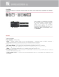
Buffalo II DAC
User Manual
Revision 1.0
Twisted Pear Audio
Overview
The Buffalo-II is a 32-bit stereo audio reference DAC module designed for uncompromising audio quality.
Based on the ESS Technology ES9018 Sabre Reference chip, the Buffalo32S accepts S/PDIF, PCM, and
DSD digital audio signals at sample rates up to 32-bit/400khz. In stereo mode the balanced stereo outputs
are made up of four parallel balanced DACs per channel. In dual mono mode all 8 balanced DACs are used
for one channel achieving the best possible dynamic range.
Power Requirements
The DAC makes extensive use of local voltage regulation with careful attention to each supply pin of the
DAC. There is only one main power supply input in the standard configuration. The VD supply requires
voltage between 5V and 5.5V with the preference toward 5.5V and it draws approximately 290ma. We
recommend using either a Placid tuned for shunting about 60ma (350ma CCS current) or half of a LDPS.
See the Placid manual for more detail.
AVCC Module
The AVCC module for the analog supply pins of the DAC is supplied. It should be connected so that the
header pins connect to the same pin on the DAC board. You will note that we use an AVCC voltage that is
slightly higher than 3.3VDC this helps use achieve slightly better dynamic range. The DAC module is
supplied with a CCS fed shunt regulator especially designed for the analog section (AVCC) of the ES9018.
This manual assumes you are using that regulator module as it has been designed specifically for the
Buffalo-II.
Configuration
Basic configuration of the Buffalo-II is performed using the DIP switches located near the power supply
input and the SPDIF switch which is near the digital inputs. The configuration DIP switch has positions
marked on and off and switches numbered 1 through 4 . Tables 1a and 1b show the switch effects. The
default is all switches “on”.
The DIP switches configure features. Power need not be cycled after changing these switches. See Tables 1a
and 1b. It is suggested you leave these “on” for default operation. The defaults were carefully chosen for
best all-around performance. For Stereo SPDIF and PCM the defaults are ideal. For DSD you may want to
change the IIR switch.
The SPDIF switch is used to connect D1 to the output of the SPDIF input comparator. It should be switched
off when not using the SPDIF comparator such as when you plan on using PCM or DSD.
The ADDRESS header is used to select the I2C address of the DAC. You should leave the header open for
the on-board controller to function correctly with the provided basic on-board firmware.
The RESET header is used to reset the DAC if necessary. This is not normally needed even when changing
registers.
The I2C header is used to communicate with the DAC from a controller such as the Volumite. It includes a
3.3V supply voltage for modules that can use it. If using the 3.3V supply do not exceed 75ma load.
DIP Switch 1
DIP Switch 2
DPLL Bandwidth
ON
N/A
Stereo.
OFF
ON
Dual Mono LEFT
OFF
OFF
Dual Mono RIGHT
Table 1a - On-Board controller Stereo/Dual Mono configuration
Switch
ON
OFF
DIP Switch 3 – FIR Roll Off
Fast
Slow
DIP Switch 4 – IIR Bandwidth
Normal (use with SPDIF/PCM)
50Khz (for DSD)
Table 1b – On-Board controller FIR and IIR settings.
Analog Characteristics
The Buffalo II does not include an output stage but is designed to mate with the IVY III current to voltage
stage. It is not recommended to use the Buffalo II output directly, but it is possible. The output can be used
as a voltage source into a high impedance but THD+N will suffer. THD+N as a voltage source is about 108db whereas when used with a very low input impedance current to voltage stage such as the IVY-III it
can achieve -120db THD+N in mono mode.
Each analog output at 0DBFS is equivalent to a voltage of approximately 92.4% of AVCC in series with
195Ω. So given 3.3VDC AVCC it will be about 3.05Vpp across 195Ω. The output will be DC biased at
AVCC/2. This works out to about 16ma peak to peak at each output. The amount of bias current will depend
of the voltage of the virtual ground.
In dual mono mode the channel on the DAC which is opposite the selected channel carries the same analog
signal but anti-phase as shown in table 2. This allows the use of the IVY-III as a single differential
(balanced) mono channel. Dual mono operation is used to achieve the best dynamic range. If you still need
single ended output then you would want to add a high quality BAL/SE converter such as the Ballsie Lite or
the Ventus.
For more detail about the IVY-III please check the IVY-III manual.
Mode
Left Differential Output
Right Differential Output
Stereo
Normal Phase
Normal Phase
Mono - Left
Normal Phase
Anti-Phase
Mono - Right
Anti-Phase
Normal Phase
Table 2 – R47-50 values and balanced output levels. Single ended levels are half the balanced levels.
Connecting Digital Sources
Consumer Level SPDIF
Connect consumer level SPDIF signals to SPDIF and GND at the input terminal block. Make sure the
SPDIF switch is closed.
TTL Level SPDIF
Make sure the SPDIF switch is open. Connect TTL level SPDIF signals to D1 and GND at the input
terminal block.
TTL Level I2S
Make sure the SPDIF switch is open. Connect I2S signals as follows:
Source GND → GND
Source Bit Clock → DCK
Source Word Clock(LRCK) → D1
Source Data → D2
TTL Level DSD
Make sure the SPDIF switch is open. Connect DSD signals as follows:
Source GND → GND
Source Bit Clock → DCK
Source Data 1(usually left) → D1
Source Data 2(usually right) → D2
Using External Controllers
When using an external controller on the I2C bus (Volumite for example) it is required to remove the onboard controller otherwise the on-board controller will interfere with communication from the external
controller.
Optional Features
The following are not recommended nor supported, but as some of you will want to tinker I am making this
information available. If you decide do this do not expect any support should your DAC fail. You are on
your own.
To use external supplies remove the ferrite bead located on the bottom side of the PCB for the supply you
wish to make external.
VDD(1.2V) remove L6
VDD_XO(3.3V) remove L7
DVCC (3.3V) remove L8
Once you have removed the ferrite bead you can supply each voltage at the marked pin header. For
convenience I added a pad for VD at each header.