1
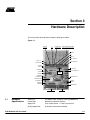
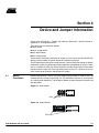
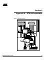
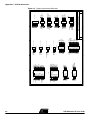
STK100 Starter Kit User Guide
--------------------------------------------------------------------------------------------------
December 1999
R
Table of Contents
Section 1
Introduction ........................................................................................... 1-1
1.1
1.2
AVR® STK100 Starter Kit..........................................................................1-1
Device Support .........................................................................................1-1
Section 2
Getting Started...................................................................................... 2-1
2.1
2.2
2.3
2.4
Unpacking the System ..............................................................................2-1
System Requirements...............................................................................2-1
Power Supply ............................................................................................2-1
Connecting the System.............................................................................2-1
Section 3
Hardware Description .......................................................................... 3-1
3.1
Hardware Specifications ...........................................................................3-1
Section 4
Device and Jumper Information............................................................ 4-1
4.1
4.2
4.3
4.4
4.5
4.6
Device Orientation ....................................................................................4-1
Jumpers ....................................................................................................4-2
The Function of the Jumpers ....................................................................4-2
Headers ....................................................................................................4-3
User Interface Headers .............................................................................4-4
Notes on Usage ........................................................................................4-5
Section 5
Installing the Software .......................................................................... 5-1
5.1
Windows® 95/98 & Windows NT® .............................................................5-1
Section 6
How to Use the Software ...................................................................... 6-1
6.1
6.2
6.3
6.4
6.5
Overview ...................................................................................................6-1
Configuring the Software ..........................................................................6-2
Loading Data.............................................................................................6-2
Programming ............................................................................................6-2
Warning.....................................................................................................6-3
Section 7
Menu and Option Descriptions ............................................................. 7-1
7.1
File Menu ..................................................................................................7-1
i
Table of Contents
7.2
7.3
7.4
7.5
7.6
Device Menu .............................................................................................7-1
Programmer Menu ....................................................................................7-1
View Menu ................................................................................................7-2
Help Menu.................................................................................................7-2
Other Controls...........................................................................................7-2
Section 8
Technical Support................................................................................. 8-1
8.1
8.2
8.3
General .....................................................................................................8-1
Registration...............................................................................................8-1
EMC Regulations ......................................................................................8-1
Section 9
Appendix A – STK100 Schematics....................................................... 9-1
ii
Section 1
Introduction
1.1
AVR STK100
Starter Kit
The STK100 Starter Kit is designed to support the AVR Microcontroller from Atmel Corporation. The system will help tiny AVR users to get started designing with AVR
Microcontrollers.
The STK100 incorporates an In-System Programming unit and an applications board.
For late breaking news and any manual errata always check the README.TXT file
included with the software or check the Atmel web site for any updates.
1.2
Device Support
The system software currently has support for the following devices.
■ ATtiny10
■
ATtiny11
■
ATtiny12
■
ATtiny15
■
ATtiny22
■
ATtiny28
■
AT90S2343
Upgrades for new devices will be available via the Internet at www.atmel.com.
STK100 Starter Kit User Guide
1-1
Introduction
1-2
STK100 Starter Kit User Guide
Section 2
Getting Started
2.1
2.2
2.3
Unpacking the
System
System
Requirements
Power Supply
You will find the following items in the pack:
■ STK100 main board
■
1 disk set
■
Parallel/printer port cable
■
ATtiny11 sample + AT90S2343
■
Atmel CD-ROM
The minimum computer hardware and software requirements are:
■ 80486 processor or above
■
16 MB RAM
■
2 MB free hard disk space
■
Windows 95/98 or Windows NT
9.5 - 15-volt DC power supply with 3.5 mm barrel connector, center positive or 7 - 13volt AC power supply with 3.5 mm barrel connector.
Note:
2.4
Connecting the
System
If the regulator or other IC runs too hot, reduce the input voltage. The specially
formulated ink used on the STK100 will turn darker if subjected to heat to indicate hot spots. It will turn lighter when the heat source is removed.
The system has two separate connections to the PC either of which may be used for
running or programming Tiny AVR devices on the STK100. The connectors for serial
and parallel port are next to each other on the STK100 board.
The two connections are serial 9-pin “D” connector connecting to the serial port or parallel 25-pin “D” connector connecting to the parallel/printer port. The programmer software
must be configured for the correct connection. This is described in Section 6, “How to
Use the Software”.
Note that in order to update the internal firmware on the STK100 for new device support,
the system must be connected to the parallel port.
In order to receive free updates, register at:
www.atmel.com/products/avrrisc/register/
STK100 Starter Kit User Guide
2-1
Getting Started
Updates will be added to the Atmel web site as new parts become available.
A parallel port cable is supplied with the system to allow this port to be used for
upgrades. If you prefer to use the serial port, a straight-through serial cable is required.
Do not use a null-modem cable with crossed connections.
The software must be configured for either serial or parallel port operation, and the
correct port chosen: LPT1, COM1, etc. See Section 6, “How to Use the Software” for
details.
Please read the next section, “Hardware Description”, before using the programmer in
STK100.
2-2
STK100 Starter Kit User Guide
Section 3
Hardware Description
The main features of the board are shown in the diagram below.
Figure 3-1.
ANALOG
J3
8-PIN SOCKET
USER PROTOTYPING AREA
PORT B
J4
PORT D
MISC HEADER
J6 AND J8
28-PIN SOCKET
20-PIN SOCKET
3.684MHz
CRYSTAL
4 SWITCHES
EXPANSION
HEADER
ISOLATION
JUMPER
AT90S8515
INFRARED
TRANSMITTER
4 LEDs ON PORT B
RESET SWITCH
PIEZO SPEAKER
ISP INTERFACE
ON/OFF
SWITCH
INFRARED
RECEIVER
POWER INPUT
PARALLEL PORT
3.1
Hardware
Specifications
STK100 Starter Kit User Guide
Serial Port:
SERIAL PORT
Full duplex, 8 bits, no parity, running at 9600 baud
Parallel Port:
Buffered synchronous interface
Supply Rail:
Fully variable from 0 - 4.7 volts (set from PC)
Analog Supply Rail:
As above, but isolated and filtered
3-1
Hardware Description
Supply Current Limit:
150 mA (approx.) independent of VCC setting
VPP Supply:
12 volts up to 10 mA
Brownout:
Tracking brownout triggers when VCC drops below 0.4V of
previous VCC setting
>9.5 volts DC input center positive
Supply:
>7 volts AC
Max supply 15VDC or 13VAC
Input via 3.5 mm barrel connector
Oscillator:
3.684 MHz crystal
General User I/O:
Four low-current LEDs connected together with four user
switches
Infrared Interface:
Receiver/demodulator with digital output (30 m range)
Sound:
Transmitter modulated by AVR ATtiny28 only,
active current limited
Piezo speaker with transistor amplification, AC coupled
Size:
3-2
User Matrix Area:
Standard Eurocard size 160 mm x 100 mm to enable
installation in a standard case
0.1" pitched holes in a 35 x 21 hole pattern
Keypad Connector:
10-key matrixed keypad connection
ISP Connector:
Standard Atmel In-System Programming interface
Expansion Connector:
For connection of external programming systems
Device Sockets:
Four 1 x 28-pin, 1 x 20-pin and 2 x 8-pin
Port Headers:
Three 2 x 10-pin and 1 x 8-pin
STK100 Starter Kit User Guide
Section 4
Device and Jumper Information
Please refer to Figure 9-2, “Targets and Interfaces Schematic”, found in Section 9,
“Appendix A – STK100 Schematics”.
The system has four sockets for devices:
■ 28-pin socket
■
20-pin analog socket
■
8-pin digital socket
■
8-pin analog socket
These sockets have been configured to accept all of the current and future AVR Tiny
devices. Please choose the correct socket for the device to program.
The STK100 features two types of programming. It will use either low-voltage In-System
Programming (ISP) or high-voltage parallel programming, depending on the part. Therefore, it is essential that the user inserts the device into the correct socket and chooses
the correct device type from the programming menu on the PC. Failure to do so may
result in damage to the device and possibly the system.
4.1
Device
Orientation
Before programming a device using the programming module, the device must be
inserted correctly into the programming unit. The AVR device itself has an arrow printed
on it, which points towards pin 1 of the device. Below are the three types of sockets and
their orientation.
Figure 4-1. 8-pin Devices
-
PIN 1
Figure 4-2. 20-pin Devices
-
PIN 1
STK100 Starter Kit User Guide
4-1
Device and Jumper Information
Figure 4-3. 28-pin Devices
28 -
PIN 1
There is another method of checking that the device is inserted the right way and that is
to check the notches on both the device and the programming socket. At the end of the
device a notch is cut out. There is also a notch cut out on the device socket, which is
also printed on the board. The notch on the device must correspond with the notch in
the socket.
The orientation of the device is vitally important. If you insert the device in the wrong
way, it may be damaged. Do not plug a device in with the power switched on: it may
damage it. Similarly, never remove the device while the power is on.
Note:
4.2
Jumpers
Do not insert a device in more than one socket at a time. Otherwise, programming errors will occur.
In addition to the sockets, there are user-accessible jumpers. J3, J4, J6 and J8 are used
to enable the additional I/O ports that are available on some devices. The jumper next to
each socket should be set towards pin 1 marked on the schematic for programming a
device using the socket, and then moved across towards pin 3 to run.
Figure 4-4. STK100 Starter Kit
Expansion Port
J8
J6
Parallel
Connector
J10
Port Headers
Serial
Connector
J3
J4
Prototyping Area
Programming
Interface
Power
Connector On/Off
Switch
4.3
The Function of
the Jumpers
4.3.1
J3
This jumper is adjacent to Socket 3 8-pin digital part and is used to select program set
towards pin 1 or run set towards pin 3. When in run mode it will enable Port PB5 and will
route it to the port B 10-pin header.
4.3.2
J4
This jumper is adjacent to Socket 4 8-pin analog part and is used to select program set
towards pin 1 or run set towards pin 3. When in run mode it will enable Port PB5 and will
route it to the port B 10-pin header.
4.3.3
J6
This jumper is adjacent to Socket 2 20-pin part and is used to select the system clock
during programming when set towards pin 1. To run, set it towards pin 3, which will allow
the port pin to be used as I/O bit PB5/ADC8.
4-2
STK100 Starter Kit User Guide
Device and Jumper Information
4.3.4
J8
This jumper is adjacent to Socket 2 20-pin part and is used to select program set
towards pin 1 or run set towards pin 3. When in run mode it will enable Port PB7/ADC10
and will route it to the port B 10-pin header.
There are also additional jumpers that can be used for special functions.
4.3.5
J10
Isolation jumpers. These jumpers are used to isolate the on-board peripherals on the
system so the user can use the port pins in their circuits.
4.3.6
Functions
Bit 0 - Bit 3
Used to disable relevant switch/LED combinations I/O
Sound
Used to disable speaker circuit output only
IRT
Used to disable infrared transmitter output only
IRR
Used to disable infrared receiver input only
Note:
4.4
Headers
Remove the jumper to disable the circuit.
There are various signals brought out for convenience from the circuit which the user
can access. These connectors are adjacent to the prototyping area. Note that the pin
numbers are screened onto the overlay.
Figure 4-5. 10-pin Connector
CUT CORNER
SHOWN ON
BOARD FOR
ORIENTATION
PIN 1
PIN 2
PIN 3
PIN 4
PIN 5
PIN 6
PIN 7
PIN 8
PIN 9
PIN 10
Figure 4-6. 8-pin Connector
CUT CORNER
SHOWN ON
BOARD FOR
ORIENTATION
STK100 Starter Kit User Guide
PIN 1
PIN 2
PIN 3
PIN 4
PIN 5
PIN 6
PIN 7
PIN 8
4-3
Device and Jumper Information
4.5
User Interface
Headers
4.5.1
J2
Matrixed Keypad Interface: This is wired directly to the 28-pin device (see
www.avr-forum.com for keypad details).
4.5.2
J5
Miscellaneous: These are miscellaneous signals that can be used in conjunction with
the port headers (see below). The signals are:
Pin 1:
PA0 on 28-pin part
4.5.3
4.5.4
4.5.5
4-4
J7
J9
J11
Pin 2:
PA1 on 28-pin part
Pin 3:
Demodulated infrared receiver input (PA3) on 28-pin part
Pin 4:
Modulated infrared transmitter output (PA2) on 28-pin part
Pin 5:
Buffer enable can be used to enable external isolation buffer during
programming (active low during programming)
Pin 6:
Reset input from user circuit (open collector or pull-down only)
Pin 7:
Ground
Pin 8:
VCC
Port D: These are the port D signals from 28-pin and 20-pin parts.
Pin 1:
PD0
Pin 2:
PD1
Pin 3:
PD2
Pin 4:
PD3
Pin 5:
PD4
Pin 6:
PD5
Pin 7:
PD6
Pin 8:
PD7
Pin 9:
Ground
Pin 10:
VCC
Port B: These are the port B signals from all parts.
Pin 1:
PB0
Pin 2:
PB1
Pin 3:
PB2
Pin 4:
PB3
Pin 5:
PB4 (AD7 input on 20-pin part)
Pin 6:
PB5 (AD8 input on 20-pin part)
Pin 7:
PB6 (AD9 input on 20-pin part)
Pin 8:
PB7 (AD10 input on 20-pin part)
Pin 9:
Ground
Pin 10:
VCC
Analog: These are the analog inputs (port A) on the 20-pin part and 8-pin analog part.
Pin 1:
PA0 (AD1 input on 8-pin part)
Pin 2:
PA1
Pin 3:
PA2
STK100 Starter Kit User Guide
Device and Jumper Information
Pin 4:
PA3 (AD2 input on 8-pin part)
Pin 5:
PA4 (AD3 input on 8-pin part)
Pin 6:
PA5 (AD0 input on 8-pin part)
Pin 7:
PA6
Pin 8:
A/D reference input
Pin 9:
Analog ground
Pin 10:
Analog supply rail
Note that additional analog inputs are available on the port B connector as shown in
parentheses on the port B connection table.
Finally, there are two expansion connectors that can be used to drive external circuits.
4.5.6
J13
ISP Connector: This will be used to enable the user to program external devices in circuit using the system. It conforms to the standard Atmel ISP pinout.
4.5.7
J12
Expansion Connector: For future use.
4.6
Notes on Usage
1. It is advisable to disconnect all user circuitry when attempting to program as it
may override the programming control signals and prevent a successful programming session.
2. Attempting to draw more than 150 mA of current from VCC will invoke the currentlimiting circuit.
3. Users are advised not to input signals larger than the VCC setting to any device
pin as it may damage the device and/or the starter kit hardware.
4. In order to supply the maximum flexibility, the LEDs and switches have been
connected together. The design is such that if the port DDRx register is set to
input (0), then the LED will be turned off and the input will be a 1. If the switch is
pressed, then the LED will light for as long as the switch is pressed and will extinguish when released. When the switch is pressed, the input on the port will be a
0. If the DDRx register bit is set to output (1), then sending a 0 out on the port will
turn the LED on and a 1 will turn it off. Note that the circuit is arranged so the
LED is brighter when the switch is pressed than when it is pulled low by the
device. It is possible to both read the switch and write to the LED by careful
manipulation of the DDRx register (set it to output for most of the time and briefly
switch to input when a switch read is required).
5. The infrared transmitter is modulated by the device and is driven directly. The
receiver has a built-in demodulator and provides a direct digital signal to the
device.
6. The keypad interface was designed for a 10-key matrixed keypad and uses the
multiplexed keypad interface on the 28-pin device.
7. Ensure the jumper next to the socket being used is set to Program or Run, as
required.
8. Programming low-voltage parts: Some 3.3-volt parts may need 5V programming
voltages, even though they run at lower voltages. We recommended that all
peripheral jumpers (J10) are removed to isolate user circuits before programming the device.
STK100 Starter Kit User Guide
4-5
Device and Jumper Information
4-6
STK100 Starter Kit User Guide
Section 5
Installing the Software
5.1
Windows 95/98 & Check web site www.atmel.com for the latest updates before installing the software.
Windows NT
To install the software please insert the supplied disk or CD-ROM in your computer and
perform the following steps:
■ Click on your “Start” button.
■
Select “Settings”.
■
Select “Control Panel”.
■
Choose “Add/Remove Programs”.
■
Click the “Install” button.
■
Follow on-screen prompts.
The software will then be installed onto your computer and an icon will be added to your
“Start” menu.
This software does not support Windows 3.11 as it is a 32-bit application.
Note:
In the unlikely event that you have any problems installing the software or
suspect that you have faulty media please contact our technical support
department for advice. Please make sure you have the latest version of the
software installed before contacting the support line.
See Section 8, “Technical Support” for more information.
STK100 Starter Kit User Guide
5-1
Installing the Software
5-2
STK100 Starter Kit User Guide
Section 6
How to Use the Software
The programmer software is shown below:
Figure 6-1.
WINDOWS
MAIN
DEVICE
SECURITY
HARDWARE
SELECTION
MENU
SELECTION
RATINGS
SELECTION
STATUS INDICATOR
MEMORY BUFFER
ASCII PANE
AND MESSAGE LINE:
WINDOW - EDITABLE
- EDITABLE
RED = ERROR
YELLOW = IN PROGRESS
GREEN = OK
6.1
Overview
STK100 Starter Kit User Guide
The programmer uses three main displays – Flash Memory, EEPROM Memory and
Status. Data and information are displayed on these three screens, which are selected
by a mouse-click on the appropriate button. The main menu gives file and programmer
operations and the configuration information is shown just below the menu bar. A status
indicator at the bottom of the screen shows whether an operation was successful – a red
light means that an error has occurred. All menu choices can be selected by using the
mouse or pressing the Alt key with the underlined letter in the menu item.
6-1
How to Use the Software
6.2
Configuring the
Software
1. The first step is to choose the type of hardware connection, using the drop-down
list at the top right of the screen. Choose STK100 (serial port) or STK100 (parallel port), depending on your requirements. Ensure that the board is connected to
the correct port – serial or parallel.
2. Now select the “Programmer - Options” menu choice. A dialog box appears
where you can pick the correct port setting. If parallel port had been selected in
stage 1, then this dialog box gives parallel port choices (LPT1, LPT2, LPT3);
otherwise, it gives serial port choices (COM1, COM2, COM3, COM4).
3. Next, select the required device in the drop-down list at the top left of the screen.
The memory sizes, fuse availability and other device-specific features are set
automatically.
4. Set the level of programming security required in the third drop-down list in the
center of the screen.
6.3
Loading Data
1. To load data to be programmed, choose the “File - Load” menu choice. A further
menu fly-out allows you to select Flash or EEPROM memory as the target for the
load operation.
Note:
Only Intel hex files can be used.
2. Select the file and it will be opened in the correct buffer window. If an error occurs
during the load operation because the file cannot be found, the file is not Intel
hex, the file is too big, etc., then the status light at the bottom left of the screen
turns red and a warning message is displayed. If the operation was successful,
this indicator light stays green. The light is yellow when the operation is taking
place – this behavior is the same for all operations. Clicking the mouse on the
error message opens the status window where more information may be given.
3. When a file has been loaded into the Flash memory, and the EEPROM memory
if required, the programmer is ready for programming operations. EEPROM data
(or Flash data) can be typed directly into the buffer windows instead of being
loaded from a file. The data can be entered as ASCII characters or as hexadecimal numbers.
6.4
6-2
Programming
The programming operations are listed in the “Device” menu. The programmer must be
configured before programming can be undertaken, and for the program operation, data
must be loaded into the buffer windows.
Figure 6-2.
STK100 Starter Kit User Guide
How to Use the Software
6.4.1
The Four Different
Operations
■
Erase device: The device is erased and code and EEPROM memories will be empty –
blank value is FFh. All fuse settings will be cleared to default values (see data
book/CD-ROM for device-specific fuse information).
■
Program device: Choose “Flash”, “EEPROM”, “Lockbits” or “Fuses” on the fly-out
menu. If “Flash” or “EEPROM” is chosen, then that part of the device is programmed
with the contents of the Flash or EEPROM buffer window, respectively. If “Lockbits” is
selected, the security bits are programmed according to the security settings dropdown list described above. If “Fuses” is chosen, a dialog box appears with the fuses
available on the selected device. Set the fuses to your requirements.
■
Read device: If “Flash” or “EEPROM” is selected, the contents of the device memory
selected is uploaded and displayed in the relevant buffer window. If the device is
blank, then all locations will read as FFh. If the security (lock)bits are set, then the
data will be invalid. Selecting “Fuses” displays the status of the fuses on the selected
device in a list box.
■
Verify device: The contents of the selected memory area (Flash or EEPROM) on the
device is compared with the contents of the equivalent buffer window and any
differences are shown in red – correct values are shown in green.
It is suggested that, for most programming sessions, Auto Program be used.
Choose “Auto Program Options” to set the required programming operations. A list of
operations (Erase, Program Flash, fuse bits, etc.) is displayed:
Figure 6-3.
Check the operations required (v = on) and all the chosen operations will be carried out
when Auto Program (F5) is used. If “Program Fuses” is checked, then another dialog
box will appear, after this list is closed, where the device-specific fuses can be set.
Note:
6.5
Warning
STK100 Starter Kit User Guide
It is advisable to erase the device before programming unless you are adding
extra data to existing data in the device. You will not be able to program the
device if the write lockbit has been set without first erasing it.
Setting lockbits may mean that you will be unable to perform further verification on the
device, and disable further writing to the device. You will, however, be able to re-use the
device if you perform an erase.
6-3
How to Use the Software
6-4
STK100 Starter Kit User Guide
Section 7
Menu and Option Descriptions
7.1
File Menu
7.1.1
Load
Select Memory Area/buffer window to load (Flash or EEPROM), then open the “Intel
Hex” file in the “Open File” dialog box. A red status warning light indicates that the file
load was unsuccessful. This may be because the file is not Intel hex or it is too large for
the selected buffer/memory.
7.1.2
Save
Saves the contents of the selected buffer (Flash or EEPROM) to file. Choose a filename
in the “File Save” dialog box that appears.
7.1.3
Reload
Reloads the buffer (Flash or EEPROM) with the last file opened.
7.1.4
Exit
Quits the program. Standard Windows close choices can also be used to exit the
program.
7.2
Device Menu
7.2.1
Erase
The whole device is erased.
7.2.2
Program
The selected device memory, fuses or lockbits are programmed.
7.2.3
Read
The selected device memory or fuses are read.
7.2.4
Verify
The selected device memory is verified against the buffer contents.
7.2.5
Run
Takes target device out of programming mode and into normal run mode. The user will
be prompted to switch jumpers to run mode.
7.2.6
Fuses
Presents the user with a list of available programmable fuses on the device and allows
the user to write and read these fuses if the device supports the program.
7.2.7
Auto Program
All operations selected in the “Auto Program Options” are carried out.
7.2.8
Auto Program
Options
Dialog box to set required programming operations that will be carried out sequentially
when “Auto Program” is pressed.
STK100 Starter Kit User Guide
7-1
Menu and Option Descriptions
7.3
Programmer
Menu
7.3.1
Options
Dialog box for port selection. You must choose parallel or serial port operation and the
correct product (STK100) first, using the drop-down list at the top right of the screen.
7.3.2
Information
Shows information about the programmer state (e.g. hardware detected), which port,
etc.
7.4
View Menu
7.4.1
Flash
The Flash Memory buffer window is displayed.
7.4.2
EEPROM
The EEPROM Memory buffer window is displayed.
7.4.3
Status
The Status window is displayed. This lists all operations, error messages, and status
information that have been posted during this session.
7.5
Help Menu
7.5.1
About
7.6
Other Controls
7.6.1
Device Selector
Located at the top left of the screen, this drop-down list is used to select the required
device. Make sure that this selection matches the device you have plugged into the
board. Obtain upgrades to support new devices as they are released.
7.6.2
Security
Located in the center of the screen, security is used to select type of access to the
device once it has been programmed. This is done by programming the lockbits, so
ensure that the lockbits are checked in the “Device - Auto Program Options” if you want
security set on the device, or choose “Device - Program - Lockbits” for manual
programming.
7.6.3
Hardware Selection
Located at the top right of the screen, the hardware selection must be set to one of the
STK100 options – serial or parallel port. Which serial or parallel port is used is set in the
“Programmer - Options” menu. Ensure that the STK100 board is connected to the correct port.
7.6.4
Window Selection
Located below the device selector, these three buttons indicate which display is visible –
Flash buffer window, EEPROM buffer window or the Status window. Whichever display
is active can also be selected using the “View” menu.
7.6.5
Flash Buffer Window Displays the Flash memory in a buffer window. The code to be programmed into the
device is loaded into this buffer by the “File - Load - Flash” option, or read from the
device by the “Device - Read - Flash” option. The size of the buffer changes to mirror the
Flash memory size on the selected device. If “Device - Verify - Flash” is used, the contents of this buffer are compared with the contents of the Flash (code) memory on the
device. Locations that match are shown in green, mis-matches are shown in red. The
data in this buffer window can be changed or entered as either hexadecimal numbers or
7-2
Version and program information
STK100 Starter Kit User Guide
Menu and Option Descriptions
ASCII characters. Holding the mouse cursor over a value brings up a fly-out that gives
the address and the value in decimal, binary, hexadecimal and ASCII.
7.6.6
EEPROM Buffer
Window
Displays the EEPROM memory in a buffer window. The code to be programmed into the
device is loaded into this buffer by the “File - Load - EEPROM” option, or read from the
device by the “Device - Read - EEPROM” option. The size of the buffer changes to mirror the EEPROM memory size on the selected device. If “Device - Verify - EEPROM” is
used, the contents of this buffer are compared with the contents of the EEPROM memory on the device. Locations that match are shown in green, mis-matches are shown in
red. The data in this buffer window can be changed or entered as either hexadecimal
numbers or ASCII characters. Holding the mouse cursor over a value brings up a fly-out
that gives the address and the value in decimal, binary, hexadecimal and ASCII.
7.6.7
Status Window
This window lists all the operations, status and error messages that have happened during the current session.
7.6.8
Status Indicator
Gives a visual result of the current operation – red means that the operation failed,
yellow means it is in progress and green means it was successful. Further information is
given in the accompanying message. These messages are listed in the Status window.
STK100 Starter Kit User Guide
7-3
Menu and Option Descriptions
7-4
STK100 Starter Kit User Guide
Section 8
Technical Support
8.1
General
A variety of technical support and user help is available to support the STK100 and AVR
devices in general.
When contacting Technical Support please specify which starter kit you require support
on – STK100, in this case. You may be asked for your registration details, so please
register the product. See below for registration details.
Telephone Number:
+44 (0) 1970 621049
Fax Number:
+44 (0) 1970 621040
e-mail:
[email protected]
We recommend that, unless your query is very simple or urgent, you use e-mail as the
preferred method of contacting Technical Support. This allows you to supply us with full
details of the problem.
If your problem is related to the PC connections, then please advise us of the PC type
(e.g. laptop, desktop), speed and operating system, software version shown in “About”
menu choice and whether you are using the serial or parallel port.
For general information on Atmel, AVR devices or other Atmel products, log on to
www.atmel.com.
For information on AVR devices, code examples, application notes, frequently asked
questions (FAQs), distributor lists and AVR resources, log on to
www.avr-forum.com.
This web site also features the AVR chat forum, where you can obtain help and advice
from other AVR users. This is not an official Atmel site, but it is endorsed by Atmel.
8.2
Registration
In order to receive updates you must be registered.
See www.atmel.com/products/avrrisc/register/.
Software updates will be added to the Atmel web site and AVR-forum web site as new
parts become available.
8.3
EMC Regulations This system has been tested to ensure that it complies with the latest regulations for
EMC susceptibility and emissions. Although the system has been tested, it is a demonstration board and the user will modify the board to his/her requirements, therefore the
EMC characteristics of the board will not remain constant. The board has been designed
to minimize electromagnetic radiation, but due to the open framework and user interface, it is not advisable to rely on an absence of EMI radiation when using this board.
STK100 Starter Kit User Guide
8-1
Technical Support
Atmel cannot be held accountable for any user-supplied equipment, such as power supplies and computers, used with this system. If these parts do not conform to the EMC
regulations, then the complete system will not conform to the standards.
The same proviso applies to any user circuitry connected to this system, such as test
boards and modules. If any changes are made to the hardware supplied with this system, such as a change in the crystal frequency or modifications to tracks or layouts, then
the system will not conform to the regulations.
8-2
STK100 Starter Kit User Guide
1
2
3
4
Parallel
P1
1
14
2
15
3
16
4
17
5
18
6
19
7
20
8
21
9
22
10
23
11
24
12
25
13
SERIAL PORT1
1
6
2
7
3
8
4
9
5
A
R16
4K7
+5
GND
R14
4K7
1
2
4
6
8
11
13
15
17
19
1
10
R15
100K
D1
LL4148
2
b
+5
VCC
1Y1
1Y2
1Y3
1Y4
2Y1
2Y2
2Y3
U2 2Y4
R13
4K7
B
B
MM74HC244WM
1A1
1A2
1A3
1A4
2A1
2A2
2A3
2A4
BE
AE
GND
+5
C1
10uF
Q1
BC858B
N
P
e
c
20
18
16
14
12
9
7
5
3
DB9
+5
4K7
R10
R7
4K7
PB5
PB6
PB7
reset
PD0
nc
PD1
PD2
PD3
PD4
PD5
U1
90S8515J
PA4
PA5
PA6
PA7
ICP
nc
ALE
OC1B
PC7
PC6
PC5
C3
33pF
STK100
EXP3
EXP2
EXP1
EXP6
EXP5
EXP4
560R
R19
560R
R18
R17
+5
560R
560R
R12
560R
R11
560R
R9
560R
R8
560R
R6
560R
R4
560R
R3
R1
Date:
Size
A
Title
3.6864Mhz
C2
27pF
D
Sunday, June 27, 1999
Document Number
E
Sheet
1
E
AVR 'Tiny' Starter Kit
Main Logic
1K
R22
560R
560R
R21
XTAL1
39
38
37
36
35
34
33
32
31
30
29
D
BUFF_EN
7
8
9
10
11
12
13
14
15
16
17
+5
VPP_EN
EXP7
MISO/BSY
560R
R20
C
C
PCLK
female
R5
4K7
R2
4K7
VCC
6
5
4
3
2
1
44
43
42
41
40
PB4
PB3
PB2
PB1
PB0
nc
VCC
PA0
PA1
PA2
PA3
PD6
PD7
XTAL2
XTAL1
GND
nc
PC0
PC1
PC2
PC3
PC4
18
19
20
21
22
23
24
25
26
27
28
STK100 Starter Kit User Guide
+
A
of
D0
4
PRST
Rev
A
MOSI/XA1
SCK/XA0
BS
WR
OE
+5
Vsel
D7
D6
D5
D4
D3
D2
D1
1
2
3
4
Section 9
Appendix A – STK100 Schematics
Figure 9-1. Main Logic Schematic
9-1
9-2
1
2
3
4
ARST
AD4
AD3
GND
DRST
D3
D4
GND
RST20
D6
ID5
D4
VCC
GND
D3
D2
D1
D0
SCK/XA0
MOSI/XA1
PD7
D0
RESET
TX
MISO/BSY
OE
WR
BS
VCC
GND
PCLK
1
2
3
4
5
6
7
8
9
10
A
1
2
3
4
1
2
3
4
1
2
3
4
5
6
7
8
9
10
11
12
13
14
A
PA0
PA1
PA3
PA2
PB7
PB6
GND
NC
VCC
PB5
PB4
PB3
PB2
PB1
VCC
PB2
PB1
PB0
VCC
PB2
PB1
PB0
8 PIN ANALOG
PB5
PB4
PB3
GND
SKT4
8 PIN DIGITAL
RESET
PB3
PB4
GND
SKT3
RESET/PB7 PA0
PB6
PA1
XTAL1/PB5 PA2
XTAL2/PB4 PA3
VCC
AGND
GND
AVCC
PB3
PA4
PB2
PA5
PB1
PA6
PB0
PA7
SKT2
28 Pin Parts
RESET
PD0
PD1
PD2
PD3
PD4
VCC
GND
XTAL1
XTAL2
PD5
PD6
PD7
PB0
SKT1
8
7
6
5
8
7
6
5
20
19
18
17
16
15
14
13
12
11
28
27
26
25
24
23
22
21
20
19
18
17
16
15
VCC
EXP1
MISO/BSY
MOSI/XA1
VCC
D2
D1
D0
EXP1
EXP2
EXP3
ADREF
AGND
AVCC
AD3
AD4
AD5
AD6
VCC
D5
D4
D3
D2
D1
PA0
PA1
IRRI
IRTI
D7
D6
GND
B
B
RESET
D0
D1
D2
D3
D4
D5
D6
D7
EXP7
GND
PCLK
GND
D0
D1
D2
D3
D4
IRTI
IRRI
RESET
RST20
D7
PCLK
20 PIN ANALOG
ID5
D5
RESET
ARST
AD5
RESET
DRST
D5
1
2
3
J3
adj to SKT3
1
2
3
adj to SKT4
1
2
3
J6
adj to SKT2
1
2
3
1
3
5
7
9
11
13
J10
2
4
6
8
10
12
14
1
3
5
7
9
11
13
15
17
19
21
23
25
2
4
6
8
10
12
14
16
18
20
22
24
26
2
4
6
8
10
12
14
16
18
20
22
24
26
C
EXPANSION_PORT
1
3
5
7
9
11
13
15
17
19
21
23
25
J12
ISOLATION JUMPERS
1
3
5
7
9
11
13
2
4
6
8
10
12
14
Date:
Size
A
VCC
SCK/XA0
MISO/BSY
MOSI/XA1
BS
WR
OE
EXP1
EXP2
EXP3
EXP4
EXP5
Title
EXP6
BIT0
BIT1
BIT2
BIT3
SOUND
IRT
IRR
adj to SKT2
20_PIN_RSEL
1
2
3
J8
20_PIN_ASEL
1
2
3
8_PIN_ASEL
1
2
3
J4
8_PIN_DSEL
1
2
3
C
D0
D1
D2
D3
OE
WR
BS
STK100
Sunday, July 18, 1999
D
2
4
6
8
1 2
3 4
5 6
7 8
9 10
J13
ANALOG
1 2
3 4
5 6
7 8
9 10
J11
PORT B
1 2
3 4
5 6
7 8
9 10
J9
PORT D
1 2
3 4
5 6
7 8
9 10
J7
MISC
1
3
5
7
KEYPAD
J5
1
2
3
4
5
6
7
E
2
4
6
8
10
2
4
6
8
10
2
4
6
8
10
2
4
6
8
10
2
4
6
8
Sheet
3
E
AVR 'Tiny' Starter Kit
of
VCC
4
EXP2
AD3
AD5
ADREF
AVCC
D1
D3
D5
D7
VCC
MISO/BSY
WR
SCK/XA0
PD7
VCC
PA1
IRTI
RESET IN
VCC
3x4 Keypad
ISP CONNECTOR
1
3
5
7
9
1
3
5
7
9
1
3
5
7
9
1
3
5
7
9
1
3
5
7
1
2
3
4
5
6
7
J2
Targets and Interfaces
MISO/BSY
OE
RESET
SCK/XA0
MOSI/XA1
EXP1
EXP3
AD4
AD6
AGND
D0
D2
D4
D6
TX
OE
BS
MOSI/XA1
PA0
IRRI
Buff_en
Document Number
D
Rev
A
1
2
3
4
Appendix A – STK100 Schematics
Figure 9-2. Targets and Interfaces Schematic
STK100 Starter Kit User Guide
1
2
3
4
VSEL
4K7
R24
RAW
2
1
+5
A
PRST
RESET
SW2
R37
4K7
R32
8K2
SENSE
R25
120K
>9VAC
>11VDC
Power
3
4
b
6
7
+
-
+
2
-
+
Q5
BC847
1
3
OCD
R33
120K
R29
120K
RESET IN
U4A
LM339D
L272
U3B
OCD
RAW
SW SPDT
RAW
5
6
C6
10uF
3
SW1
13
1
2
1
2
B
C10
330pF
R30
120K
1N4001
1N4001
D5
1N4001
D4
1N4001
D3
D2
2
1
2
1
-
+
1
10
11
U4D
LM339D
10K
R34
RAW
C8
10uF (35V)
8
7
-
+
R38
10K
D9
TMMBAT42
Q3
BC847
e
+5
C11
10uF (Tant)
c
L272
1
RAW
U3A
VIN
AGND
1
470uF
C4
+
3R9 0.5W
2
REG1
LM7805
+
GND
3
1
2
4
P
N
3
12
b
2
4
N
P
2
C
LL4148
D10
8
9
4
5
2
-
+
-
+
1
2
+5
C9
1
SENSE
100R
R39
+5
+
LED1
Power
R23
1K
BZX79C12
Z1
D8
LL4148
Date:
Size
A
Title
10uF (35V)
14
U4C
LM339D
2
+5
C5
470nF
LL4148
D7
D6
LL4148
CD2
100nF
U4B
LM339D
CD1
100nF
VOUT
R35
10K
R27
C
2
1
2
1
J1
c
e
P
N
B
3
12
2
1
P
N
3
12
3
12
2
11
Q4
BC847
b
e
VCC
CD3
100nF
+5
R28
10K
R36
10K
100R
R26
CD4
100nF
CD5
100nF
AVCC
CD6
100nF
VPP_EN
RESET
C7
100nF
VCC
E
STK100
D
Saturday, June 26, 1999
Sheet
2
E
AVR 'Tiny' Starter Kit
of
4
Power Supply, Brownout and Reset
R31
1K
Q2
BC847
c
D
Document Number
2
b
c
e
STK100 Starter Kit User Guide
+
A
Rev
A
CD7
100nF
1
2
3
4
Appendix A – STK100 Schematics
Figure 9-3. Power Supply Schematic
9-3
1
2
3
4
BIT3
GND
560R
R44
A
+5
2
1
4
3
1
2
SW3
BIT3
BIT2
LED2
BIT3
R40
560R
IRT
560R
R45
B
330R
R52
+5
2
1
4
3
1
2
BIT1
VCC
b
D12
LL4148
D11
LL4148
VCC
SW4
BIT2
R50
10R
560R
R46
IRT1
SFH415T
Q7
BC847
VCC
Piezo Sounder
LED3
BIT2
R41
560R
C
C
+5
2
1
4
3
1
2
SW5
BIT1
BIT0
LED4
BIT1
R42
560R
+
Date:
Size
A
Title
C13
47uF
560R
R47
+5
+5
D
2
1
4
3
1K
D
Sunday, June 27, 1999
Document Number
STK100
IRX1
1
IS1U621
R51
SW6
BIT0
SOUND
LED5
BIT0
R43
560R
R49
470R
1
2
C12
IRR
1uF
N
R48
1K
b
+5
E
Sheet
4
E
P
N
of
4
LS1
Q6
BC847
AVR 'Tiny' Starter Kit
Peripherals
P
+
+5
2
1
2
1
P
N
B
c
2e
1
3
2
c
9-4
e
A
Rev
A
1
2
3
4
Appendix A – STK100 Schematics
Figure 9-4. Peripheral Schematic
STK100 Starter Kit User Guide
Appendix A – STK100 Schematics
STK100 Starter Kit User Guide
9-5
Appendix A – STK100 Schematics
9-6
STK100 Starter Kit User Guide
Atmel Headquarters
Atmel Operations
Corporate Headquarters
Atmel Colorado Springs
2325 Orchard Parkway
San Jose, CA 95131
TEL (408) 441-0311
FAX (408) 487-2600
Europe
1150 E. Cheyenne Mtn. Blvd.
Colorado Springs, CO 80906
TEL (719) 576-3300
FAX (719) 540-1759
Atmel Rousset
Atmel U.K., Ltd.
Coliseum Business Centre
Riverside Way
Camberley, Surrey GU15 3YL
England
TEL (44) 1276-686-677
FAX (44) 1276-686-697
Zone Industrielle
13106 Rousset Cedex
France
TEL (33) 4-4253-6000
FAX (33) 4-4253-6001
Asia
Atmel Asia, Ltd.
Room 1219
Chinachem Golden Plaza
77 Mody Road Tsimhatsui
East Kowloon
Hong Kong
TEL (852) 2721-9778
FAX (852) 2722-1369
Japan
Atmel Japan K.K.
9F, Tonetsu Shinkawa Bldg.
1-24-8 Shinkawa
Chuo-ku, Tokyo 104-0033
Japan
TEL (81) 3-3523-3551
FAX (81) 3-3523-7581
Fax-on-Demand
North America:
1-(800) 292-8635
International:
1-(408) 441-0732
e-mail
[email protected]
Web Site
http://www.atmel.com
BBS
1-(408) 436-4309
© Atmel Corporation 1999.
Atmel Corporation makes no warranty for the use of its products, other than those expressly contained in the Company’s standard warranty which is detailed in Atmel’s Terms and Conditions located on the Company’s web site. The Company assumes no responsibility for
any errors which may appear in this document, reserves the right to change devices or specifications detailed herein at any time without
notice, and does not make any commitment to update the information contained herein. No licenses to patents or other intellectual property of Atmel are granted by the Company in connection with the sale of Atmel products, expressly or by implication. Atmel’s products are
not authorized for use as critical components in life suppor t devices or systems.
Marks bearing
®
and/or
™
are registered trademarks and trademarks of Atmel Corporation.
Terms and product names in this document may be trademarks of others.
Printed on recycled paper.
1481A–12/99/1M