1
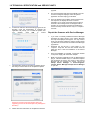
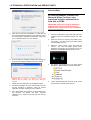
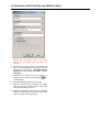
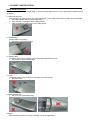
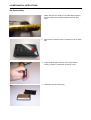
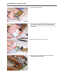
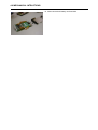
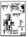
Micro Audio Jukebox
HDD1420/1620/1630/1635/1830/1835
All version
Service Manual
TABLE OF CONTENTS
Chapter
Technical Specification and Service hints.…………………1
Safety Instructions………………………………………………2
Instructions for Use……………………………………………. 3
Mechanical Instructions………………………………………. 4
Exploded view and Service parts list…………………...….. 5
Troubleshooting flow.…………………………………………. 6
Overall Block diagram…………………………………………. 7
Overall Electrical diagram……………………………………. 8
IRIS CODE…………………………………………………………9
Revision list……………………………………………………… 10
©Copyright 2005 Philips Consumer Electronics B.V. Eindhoven, The Netherlands
All rights reserved. No part of this publication may by reproduced, stored in a
retrieval system or transmitted, in any form or by any means, electronics,
mechanical, photocopying, or otherwise without the prior permission of Philips
3141 785 30705
Version 1.5
1.0 TECHNICAL SPECIFICATION and SERVICE HINTS
General
Dimensions (WxHxD) :
Weight :
Output power :
Frequency response :
Equalizer :
Hard disk :
Capacity :
Display :
Supported playback format
53.7 X 86.0 X 16.3 mm
(2.11 x 3.39 x 0.64 inch)
87 g
2 x 5 mW (16 Ohm)
20 – 16 000 Hs
5-bands
4GB – 6GB
128 x 128 pixels, 65K color
Backlight :
Battery :
White
630 mAh Li-Ion
rechargeable battery
Battery life time:
File transfer rate using
USB2.0 :
Battery charging current
>16hrs
>4Mbyte
Maximum charging time :
4hr
Battery cutoff voltage:
Connections:
3.7V
Headphone Line Out Jack
Power Connector
Yes
ID3-tag support :
USB
PC Connectivity :
File Transfer
via Windows Media Player 10 for music and picture
playback or Windows Explorer for general data (music
playback disabled)
Firmware and software upgrades
450mA
Battery level detection
Detection Level
4-step to 3-step voltage
3-step to 2-step voltage
2-step to 1-step voltage
Force Power Off voltage
8 - 320 Kbps and VBR
32 - 192 Kbps
8, 11.025, 16, 22.050
32, 44.1, 48
MP3 :
WMA :
Sample rates :
Typ.
3.6 – 3.7V
3.53 – 3.6V
3.48 – 3.53V
<3.5V
1.
If you have not already installed the Device Manager
download the latest version of the Device Manager
from http://www.philips.com/support. You may need to
enter your language preference and the model number
e.g.HDD1630, to access the Device/Firmware Manager
upgrade file.
2.
Download the zip file into a temp folder in your
computer. Unzip the file and then double click the
Setup.exe file to start the installation of the Device
Manager.
3.
Once the installation is complete, connect the GoGear
to the power supply with the AC/DC adapter.
4.
Make sure all other applications such as Philips Device
plug-in, Windows Media Player or Windows Explorer
that accessing the device are closed or else Device
Manager will not recognize the device. Launch the
Philips Device Manager at Start->Programs>Philips Device Manager->Philips Device Manager
on your PC.
5.
Click
Current consumption
DC-IN SUPPLY (4.5V)
Battery Charging Current
450mA
BATT. SUPPLY (3.7V)
Power Off
300uA
Idle
30mA
Playback without HDD reading
30mA
Playback with HDD reading
345mA
File transfer using USB2.0
350mA
Update
in
the
dialogue
box
Headphone out (headphone output load 2x16 ohm)
Maximum output power :
Frequency response :
SNR (A-wght) :
THD (1kHz) :
Left-Right Channel
Separation :
Left-Right Channel
Balance :
10 mW
45Hz – 16kHz (16Ω load)
20Hz – 16kHz (15kΩ load)
85dB
0.1%
45dB typ. (1k Hz)
40dB typ. (20Hz – 16kHz)
<1.0dB (1k Hz)
<2.0dB (20Hz – 16kHz)
the Philips Device Manager will detect the connection
of your GoGear and the application will automatically
check on the server to see if an update is available and
prompt user to download the updated firmware. Click
YES
to
start
the
downloading.
1.0 TECHNICAL SPECIFICATION and SERVICE HINTS
upgrade.
9.
The Device Manager will close automatically once the
success message is displayed. Close all opened
application and then unplug your GoGear.
10. Once the GoGear micro jukebox is disconnected from
6.
7.
A status bar will show the downloading progress of the
firmware. Once the downloading is complete the
application will prompt you to install the update onto
your
GoGear.
Click
YES
to
confirm
The application will show the status of updating and at
the end you need to click OK to complete the update.
(Please do not disconnect the jukebox during the
upgrading process as this interruption may damage the
firmware!)
8.
Follow all screen instructions to complete the firmware
the computer, the display will show “Firmware
Upgrading” for a couple of seconds and then start up
as usual. If the message does not disappear after 2
minutes, do a soft reset by pressing and holding the
Power on/off key and the volume + key for a couple of
seconds.
Repair the firmware with Device Manager
1.
If you have not already installed the Device Manager
download the latest version of the Device Manager
from http://www.philips.com/support. You may need to
enter your language preference and the model number
e.g.HDD1630, to access the Device/Firmware Manager
upgrade file.
2.
Download the zip file into a temp folder in your
computer. Unzip the file and then double click the
Setup.exe file to start the installation of the Device
Manager.
3.
Once the installation is complete, connect the GoGear
to the power supply with the AC/DC adapter.
4.
Make sure all other applications such as Philips Device
plug-in, Windows Media Player or Windows Explorer
that accessing the device are closed or else Device
Manager will not recognize the device. Launch the
Philips Device Manager at Start->Programs>Philips Device Manager->Philips Device Manager
on your PC.
1.0 TECHNICAL SPECIFICATION and SERVICE HINTS
Service Hints
Re Rebuild database, firmware and
Microsoft (Plays For Sure) copy
protection key after replacement of
hard disk or PCBA
IMPORTANT: All devices having the hard disk or
PCBA replaced must have the firmware image,
database and the Plays For Sure key rebuilt before
returning to customers.
5.
6.
Click YES to start the downloading. A status bar will
show the downloading progress of the firmware. Once
the downloading is complete the application will prompt
you to install the update onto your GoGear.
1.
Connect the GoGear to the power supply and the
computer with the combined charger and USB
cable.
2.
Reset the device by pressing and holding down
the Volume + and the power on/off slider switch
until the display turns off.
3.
While the device restart, press and hold the
volume – key until the Philips splash screen
disappear and showing the connection icon to put
the device in USB Mass Storage Device mode.
4.
The device will be listed as a new drive named
GOGEAR or MDJUKEBOX in Windows Explorer.
5.
Launch Windows Explorer and then quick format
the new drive to the file system FAT32.
Once the repair is complete a dialogue box will pop up;
click OK and unplug the GoGear from the computer.
IMPORTANT: All music & content of your micro
jukebox will be erased once the factory setting is
restored.
7.
Follow all screen instructions to complete the repair.
8.
The Device Manager will close automatically once the
success message is displayed. Close all opened
application and then unplug your micro jukebox.
9.
Once the GoGear micro jukebox is disconnected from
the computer, the display will show “Firmware
Upgrading” for a couple of seconds and then start up
as usual.
1.0 TECHNICAL SPECIFICATION and SERVICE HINTS
IMPORTANT: All music & content of your micro
jukebox will be erased once the device is
formatted.
6.
Unzip and copy all the content of the shipment ui
files of the corresponding model version into the
root directory of the device. (CD ROM with the
Shipment ui files will be provided to repair
workshops.)
7.
Disconnect the GoGear from the computer by
clicking on the safely remove hardware
on the task tray.
icon
8.
Wait until the display shows “Burn success”.
9.
Reset the device again by pressing and holding
down the Volume + and the power on/off slider
switch until the display turns off.
10. Upgrade the firmware of the device to the latest
version by following the procedure as mentioned
under “Firmware software upgrades”
2.0 SAFTETY INSTRUCTIONS
GB
NL
ESD
WARNING
Alle IC’s en vele andere halfgeleiders zijn
gevoelig voor electrostatische ontladingen
(ESD).
Onzorgvuldig behandelen tijdens reparatie kan
de levensduur drastisch doen verminderen.
Zorg ervoor dat u tijdens reparatie via een
polsband met weerstand verbonden bent met
hetzelfde potentiaal als de massa van het
apparaat.
Houd componenten en hulpmiddelen ook op
ditzelfde potentiaal.
All ICs and many other semi-conductors are
susceptible to electrostatic discharges (ESD).
Careless handling during repair can reduce life
drastically.
When repairing, make sure that you are
connected with the same potential as the mass
of the set via a wrist wrap with resistance.
Keep components and tools also at this
potential.
F
WAARSCHUWING
ATTENTION
I
Tous les IC et beaucoup d’autres
semi-conducteurs sont sensibles aux
décharges statiques (ESD).
Leur longévité pourrait être considérablement
écourtée par le fait qu’aucune précaution n’est
prise à leur manipulation.
Lors de réparations, s’assurer de bien être relié
au même potentiel que la masse de l’appareil et
enfiler le bracelet serti d’une résistance de
sécurité.
Veiller à ce que les composants ainsi que les
outils que l’on utilise soient également à ce
potentiel.
D
AVVERTIMENTO
WARNUNG
Alle ICs und viele andere Halbleiter sind
empfindlich gegenüber elektrostatischen
Entladungen (ESD).
Unsorgfältige Behandlung im Reparaturfall kan
die Lebensdauer drastisch reduzieren.
Veranlassen Sie, dass Sie im Reparaturfall über
ein Pulsarmband mit Widerstand verbunden
sind mit dem gleichen Potential wie die Masse
des Gerätes.
Bauteile und Hilfsmittel auch auf dieses gleiche
Potential halten.
Tutti IC e parecchi semi-conduttori sono
sensibili alle scariche statiche (ESD).
La loro longevità potrebbe essere fortemente
ridatta in caso di non osservazione della più
grande cauzione alla loro manipolazione.
Durante le riparazioni occorre quindi essere
collegato allo stesso potenziale che quello della
massa dell’apparecchio tramite un braccialetto
a resistenza.
Assicurarsi che i componenti e anche gli utensili
con quali si lavora siano anche a questo
potenziale.
GB
Safety regulations require that the set be restored to its original
condition and that parts which are identical with those specified,
be used.
“Pour votre sécurité, ces documents
doivent être utilisés par des spécialistes agréés, seuls habilités à réparer
votre appareil en panne”.
NL
Veiligheidsbepalingen vereisen, dat het apparaat bij reparatie in
zijn oorspronkelijke toestand wordt teruggebracht en dat onderdelen,
identiek aan de gespecificeerde, worden toegepast.
CLASS 1
LASER PRODUCT
3122 110 03420
F
Les normes de sécurité exigent que l’appareil soit remis à l’état
d’origine et que soient utiliséés les piéces de rechange identiques
à celles spécifiées.
GB
Warning !
Invisible laser radiation when open.
Avoid direct exposure to beam.
D
Bei jeder Reparatur sind die geltenden Sicherheitsvorschriften zu
beachten. Der Original zustand des Geräts darf nicht verändert werden;
für Reparaturen sind Original-Ersatzteile zu verwenden.
S
Varning !
Osynlig laserstrålning när apparaten är öppnad och spärren
är urkopplad. Betrakta ej strålen.
SF Varoitus !
I
Le norme di sicurezza esigono che l’apparecchio venga rimesso
nelle condizioni originali e che siano utilizzati i pezzi di ricambio
identici a quelli specificati.
Avatussa laitteessa ja suojalukituksen ohitettaessa olet alttiina
näkymättömälle laserisäteilylle. Älä katso säteeseen!
DK Advarse !
"After servicing and before returning set to customer perform a
leakage current measurement test from all exposed metal parts to
earth ground to assure no shock hazard exist. The leakage current
must not exceed 0.5mA."
Usynlig laserstråling ved åbning når sikkerhedsafbrydere er
ude af funktion. Undgå udsaettelse for stråling.
2.0 SAFETY INSTRUCTIONS
Battery Handling Guideline
Since the battery is packed in soft package, to ensure its better performance, it’s very important to carefully handle
the battery
2.1 Soft Aluminium foil
The soft aluminum packing foil is very easily damaged by sharp edge parts such as Ni-tabs, pins and needles.
• Don’t strike battery with any sharp edge parts
• Trim your nail or wear glove before taking battery
• Clean worktable to make sure no any sharp particle
2.2 Sealed edge
Sealing edge is very flimsy
• Don’t bend or fold sealing edge
2.3 Folding edge
The folding edge is form in battery process and passed all hermetic test.
• Don’t open or deform folding edge
2.4 Tabs
The battery tabs are not so stubborn especially for aluminum tab.
• Don’t bend tab
2.5 Mechanical shock
• Don’t Fall, hit, bend battery body
2.6 Short
Short terminals of battery is strictly prohibited, it may damage battery.
3.0 INSTRUCTION FOR USE
Power Connector
4.0 MECHANICAL INTRUCTIONS
Set Disassembly
1. Add a tape over the knobs on two side before opening
the set to prevent the knobs will fall out the set after
open.
2. Remove the cosmetic screw on the back cover by Allen
Key.
3. Finger inset the gap of the top cover assy and the
housing, and then carefully lift up the top cover.
4. Generally remove the housing.
4.0 MECHANICAL INTRUCTIONS
5. Remove the 4 screws on four corners. See pointed
arrows.
6. Carefully pull out the mainboard assy, which include the
HDD drive, LCD, battery and PCBA board.
7. Disconnect the flex cable from the front touch screen
module carefully, then free the top cover assy.
8. Lift up the double side tape of the side buttons.
4.0 MECHANICAL INTRUCTIONS
9. Turn to the bottom side.
10. Open up the metal shielding and disconnect the cable
connected to the battery. Carefully disassemble the
mini mic as circled in the picture from the plastic audio
jack holder.
11. Remove the battery part form PCBA.
12. Lift up the hard disk and disconnect the flex cable
underneath from the PCBA.
4.0 MECHANICAL INTRUCTIONS
13. After remove both battery and hard disk.
5.0 EXPLODED VIEW AND SERVICE PARTS LIST
113
102
101
103
112
106
118
114
108
109
110
111
112
113
114
107
108
100
100
101
102
103
104
105
106
107
111
115
104
115
116
117
118
105
109
110
116
MECHANICAL PARTS
994000003554 COSMETIC SREW PHOENIX
994000003555 BACK CABINET PHOENIX
994000003559 AUDIO JACK HOLDER ASSY
994000003556 SHIELDING PHOENIX
994000003572 CRADLE HOLDER PHOENIX
994000003558 SCREW 1.7X5 PHOENIX
994000003557 BATTERY PACK PHOENIX
282206200084 HDD 4GB (HDD1420/00)
282206200079 HDD 6GB (HDD1620/00/05,
HDD1630/17 & HDD1635/17)
994000003563 HDD DAMPER PHOENIX
994000003564 HDD HOLDER PHOENIX
994000003568 HD FPC PHOENIX
994000003565 FFC PHOENIX
994000003566 KEY FPC 1 PHOENIX
994000003567 KEY FPC 2 PHOENIX
994000003569 PCBA W/Z RADIO LCD PHOENIX
(HDD1630/17 & HDD1635/17)
994000003571 PCBA W/O RADIO LCE PHOENIX
(HDD1420/00 & HDD1620/00/05)
994000003573 RIGHT SIDE KEYPAD PHOENIX
994000003574 HOLD KEY PHOENIX
994000003575 LEFT SIDE KEYPAD PHOENIX
994000003576 HOUSING TOUCHPAD PHOENIX
117
MISCELLENEOUS
994000003527 EARPHONE SHE9500
994000003577 AC ADAPTOR AD7150/00 (FOR /00)
994000003578 AC ADAPTOR AD7153/17 (FOR /17)
994000003579 AC ADAPTOR AD715B/05 (FOR /05)
994000003791 CRADLE ASSY PHOENIX (FOR
HDD1635/17 ONLY)
994000003877 CD-PHX-EU (FOR /00 & /05)
994000003878 CD-PHX-US (FOR /17)
994000003876 POUCH FOR PHOENIX
994000005704 CONTROL CASE PAC001 (FOR
HDD1835/17 ONLY)
996500039152 PHOENIX RESET LABEL
5.0 EXPLODED VIEW AND SERVICE PARTS LIST
100
102
105
101
106
100
101
102
103
104
105
106
107
112
113
116
115
103
108
109
110
111
112
113
114
104
107
115
116
117
118
MECHANICAL PARTS
994000003554 COSMETIC SREW PHOENIX
994000003555 BACK CABINET PHOENIX
994000003559 AUDIO JACK HOLDER ASSY
994000003556 SHIELDING PHOENIX
994000003572 CRADLE HOLDER PHOENIX
994000003558 SCREW 1.7X5 PHOENIX
994000003557 BATTERY PACK PHOENIX
282206200084 HDD 4GB (HDD1420/00)
282206200079 HDD 6GB (HDD1620/00/05,
HDD1630/17 & HDD1635/17)
994000003563 HDD DAMPER PHOENIX
994000003564 HDD HOLDER PHOENIX
994000003568 HD FPC PHOENIX
994000003565 FFC PHOENIX
994000003566 KEY FPC 1 PHOENIX
994000003567 KEY FPC 2 PHOENIX
994000003569 PCBA W/Z RADIO LCD PHOENIX
(HDD1630/17 & HDD1635/17)
994000003571 PCBA W/O RADIO LCE PHOENIX
(HDD1420/00 & HDD1620/00/05)
994000003573 RIGHT SIDE KEYPAD PHOENIX
994000003574 HOLD KEY PHOENIX
994000003575 LEFT SIDE KEYPAD PHOENIX
994000003576 HOUSING TOUCHPAD PHOENIX
114
118
118
117
MISCELLENEOUS
994000003527 EARPHONE SHE9500
994000003577 AC ADAPTOR AD7150/00 (FOR /00)
994000003578 AC ADAPTOR AD7153/17 (FOR /17)
994000003579 AC ADAPTOR AD715B/05 (FOR /05)
994000003791 CRADLE ASSY PHOENIX
(HDD1635/17)
994000003877 CD-PHX-EU (FOR /00 & /05)
994000003878 CD-PHX-US (FOR /17)
994000003876 POUCH FOR PHOENIX
994000005704 CONTROL CASE PAC001 (FOR
HDD1835/17 ONLY)
996500039152 PHOENIX RESET LABEL
6.0 TROUBLESHOOTING FLOW
SYMPTOM 1: NO POWER
6.0 TROUBLESHOOTING FLOW
SYMPTOM 2: JUKEBOX FREEZES / HANGS UP
Open up the unit, unplug battery
connector and reconnect again
6.0 TROUBLESHOOTING FLOW
SYMPTOM 3: ERROR MESSAGE SCROLLS ON THE DISPLAY
6.0 TROUBLESHOOTING FLOW
SYMPTOM 4: NO SOUND
7.0 BLOCK DIAGRAM
3
+1.2V
1
4
XM2_ROM.RDY
XM2_MIO.RDY
XM2_DQML#
XM2_DQMH#
XM2_ROM.CS1#
4
8
TP505
1
TP504
1
XM2_CKE
Cradle_in_SW#
6
G1
G3
E4
G2
MBID0
MBID1
MUTE
MBID2
4/8 IR function remove
TouchPad Power Enable
6
4,7
RESET#
RESERVED
RESET#
XM2_ROM.RDY
5
1
1
2
R604
100K
0402
1
2
1
1
2
1
1
1
C37
0.1U
0402
16V
+80-20%
C46
C60
2
0.1U
0402
16V
+80-20%
2
2
C51
2
C58
0.1U/NA
0402
16V
+80-20%
2
1
C69
Remove damp Res.
1
Place Close Each Power Pin
XTAL_32K.IN
0.1U
0402
16V
+80-20%
0.1U
0402
16V
+80-20%
10U
0805
6.3V
10%
B
U1
T3
U2
R4
1
1
R590
U14 S2_R 2
T14
U15
R15
0
0402
1
1
TP9
TP3
USBID-DEV/HOST#
DC-DC_RUN
5
STAT2
5
TP11
AT3_PWR.OFF
OC_CRL_PWR#
C68
0.1U
0402
16V
+80-20%
C55
0.1U
0402
16V
+80-20%
ADC_EN#
R90
100K
0402
6
1
A
K
REMOTE_JACK
4,6
1PS79SB30
SOD523
5
1
TP507
5VREG_ON
10U
0805
6.3V
10%
R61
0402
1M 5%
1
8
D511
C63
0.1U
0402
16V
+80-20%
ADC_EN#_M
HD_ON/OFF#
5
1
1
C64
0.1U
0402
16V
+80-20%
Q502A
AO7600
SC70_6_EIAJ
1
DTV_RESET#
C66
0.1U
0402
16V
+80-20%
2
C38
0.1U
0402
16V
+80-20%
2
C39
0.1U
0402
16V
+80-20%
27M_OFF#
unused_only pull high
LCD_RS
STAT1
5
Current_Set
Place Close Each Power Pin
C67
7
VCC_BATR
U16
REMOTE_JACK_D
U17
R557
T15
0402
BKLT_PWM
8
T16 GP4 2 0/NA
1
GPIO4
4,7
R560 0 0402
B16
A16 CSC 2
1
B15
OC_CRL_PWR#
A15
+3.3V
1
AT3_HA2
7
AT3_HA1
7
AT3_HA0
7
AT3_HIOW#
7
AT3_HIOR#
7
AT3_HIORDY
7
AT3_HRESET#
7
AT3_HIRQ.0
7
AT3_HIRQ.1
7
AT3_HDMARQ
7
AT3_HDMACK#
7
AT3_HCS0#
7
AT3_HCS1#
7
1
K1
K3
J3
R3
T1
J2
H3
J4
J1
R2
T2
L4
L3
2
When Power-off reduce
the power loss
R67
39K
0402
1%
VCC_BATC
2
15K
R564
0402
C71
1%
0.1U
0402
16V
+80-20%
3
Q502B
7
VCC_BAT
4
AO7600
SC70_6_EIAJ
Battery Shuntdown point detect
Now:3.5V
A
+3.3V
2
1
with FM w/o FM
R608
100K
0402
VCC_MEM
For EMI & close PP5022
PP5022
BGA240_21_065MM
R607
100K/NA
0402
R606
100K
0402
2
2
2
B17
E16
E14
AVDD
E9
F6
F9
F12
J5
J6
J12
J13
M6
M9
M12
N9
E6
E7
E8
E10
E11
E12
F5
F13
G5
G7
G9
G11
G13
H5
H8
H10
H13
J7
J9
J11
K5
K8
K10
K13
L5
L7
L9
L11
L13
M5
M13
N6
N7
N8
N10
N11
N12
7
MBID0
0
0
MBID1
0
0
MBID2
0
1
R556
10K
0402
1%
REMOTE_JACK_D
Title
Phoenix DVT R0D
2
2
1
R550
CD3_BCLK
CD3_C2PO
CD3_DATA
CD3_LRCK
AT3_HD[0:15]
6/24
2
1
MBID0
MBID1
MBID2
1
0402
XM2_MIO.RDY
1%
6.81K
2
1K
0402
5% 2
1
2
R554
R605
100K/NA
0402
2
R603
100K/NA
0402
VCC_MEM
1
1
1
+3.3V
A
ADC_AIN.0
ADC_AIN.1
PM3_PWM0
PM3_PWM1
IR3_RXD
IR3_TXD
C16
C15
RESET#
pin R15=>LCD_RS
UA3_TXD
UA3_RXD
UA3_CTS
UA3_RTS
G4
H1
TP_PWR#
OT3_Y.UD
OT3_Y.CK
OT3_X.UD
OT3_X.CK
4/8
D1
XM2_SDR_CS0#
7
7
C569
0.1U
0402
16V
+80-20%
Check=>Reserved
XTAL_33M.IN
AT3_HD15
AT3_HD14
AT3_HD13
AT3_HD12
AT3_HD11
AT3_HD10
AT3_HD9
AT3_HD8
AT3_HD7
AT3_HD6
AT3_HD5
AT3_HD4
AT3_HD3
AT3_HD2
AT3_HD1
AT3_HD0
R574
10K/NA
0402
5%
S1
4
XM2_SDR_CS1#
AT3_S.HDMACK#
AT3_H.DMARQ
AT3_S.HIOR#
AT3_S.HIOW#
4
4
USB_DP
USB_DN
1
0
R586
0402
5%
5
4
4
CLK_SYS.OUT
XM2_RE_N
XM2_WE_N
XM2_ROM.RDY
XM2_MIO.RDY
XM2_WMSK1
XM2_WMSK2
XM2_CS.A#
XM2_CS.B#
XM2_CS.C#
XM2_CS.D#
XM2_CKE
TP509
4
C563
1U/NA
0603
G2
XM2_ROM.RD#
XM2_ROM.WR#
XM2_ROM.RDY
1
VBUS
RC removed
2
XTAL_32K.IN
XTAL_24M.OUT
XTAL_24M.IN
HOLD
xxxxx
ACK
PWR_ON_OFF#
View
xxxxx
xxxxx
CLK
DATA
Like Music
Volume down
Volume up
Recording
S2
2
4
4
4
D7
C8
C9
B14
A14
B7
A5
C14
B13
A8
B8
A7
CLK_24M.CODEC_R
TP13
TP506
P2
R1
P1
N2
P3
N1
M2
N3
P4
N4
M1
L2
M3
L1
M4
K2
4,6,7,8
6
Battery_ID:Low=>Plug-In
7
USB_RBIAS
USBS_DP
USBS_DN
VBUS_SENSE
1
1
I2C_CLK
C
G1
C57
10P
0402
+/-10%
50V
CLK_SYS.OUTR
AT3_HA2
AT3_HA1
AT3_HA0
AT3_HIOW#
AT3_HIOR#
AT3_HIORDY
AT3_HRESET#
AT3_HIRQ.0
AT3_HIRQ.1
AT3_HDMARQ
AT3_HDMACK#
AT3_HCS0#
AT3_HCS1#
CLK_24M.CODEC
C20
10P
0402
+/-10%
50V
2 0402
1
I2C_C_EN
2
KSI12
KSI11
KSI10
KSI9
KSI8
KSI7
KSI6
KSI5
KSI4
KSI3
KSI2
KSI1
KSI0
D2
CLK_SYS.OUT
1
4
33
0402
5% 2
AT3_HD15
AT3_HD14
AT3_HD13
AT3_HD12
AT3_HD11
AT3_HD10
AT3_HD09
AT3_HD08
AT3_HD07
AT3_HD06
AT3_HD05
AT3_HD04
AT3_HD03
AT3_HD02
AT3_HD01
AT3_HD00
100K
6
6
6
6
2
R55
XM2_MA25
XM2_MA24
XM2_MA23
XM2_MA22
XM2_MA21
XM2_MA20
XM2_MA19
XM2_MA18
XM2_MA17
XM2_MA16
XM2_MA15
XM2_MA14
XM2_MA13
XM2_MA12
XM2_MA11
XM2_MA10
XM2_MA09
XM2_MA08
XM2_MA07
XM2_MA06
XM2_MA05
XM2_MA04
XM2_MA03
XM2_MA02
XM2_MA01
XM2_MA00
R566
2M
0402
1%
33
0402
5% 2
2
PSEL1
BKL_ON
XM2_MA20_1
XM2_MA19
XM2_MA18/WE#
XM2_MA17/CAS0#
XM2_MA16/RAS0#
XM2_MA15
XM2_MA14
XM2_MA13
XM2_MA12
XM2_MA11
XM2_MA10
XM2_MA9
XM2_MA8
XM2_MA7
XM2_MA6
XM2_MA5
XM2_MA4
XM2_MA3
XM2_MA2
XM2_MA1
B
1
D3
D1
E2
E1
F2
F3
E3
F1
A6
C6
C7
A9
B9
B10
C10
A10
C11
D11
A11
C12
B11
A12
C13
D13
A13
B12
CLK_SUS.OUT
XTAL_32K.OUT
XTAL_32K.IN
XTAL_24M.OUT
XTAL_24M.IN
XTAL_33M.OUT
XTAL_33M.IN
D12
F14
E15
G15
G16
H15
H16
R538
5%
VBUS_Detect
1
8
4
4
4
4
5
PSEL1
BKL_ON
XM2_MA20_1
XM2_MA19
XM2_MA18/WE#
XM2_MA17/CAS0#
XM2_MA26
XM2_MA25
BZZ_PWM
USB_RREF
USB_DP
USB_DM
USB_VBUS
C17
E17
D17
F17
1
1
R576
1M
0402
1%
6
USB wakeup&detect
2
XM2_MA[1..15]
XM2_MA[1..15]
XM2_MA16/RAS0#
XM2_MA26
XM2_MA25
BZZ_PWM
XM2_MD15
XM2_MD14
XM2_MD13
XM2_MD12
XM2_MD11
XM2_MD10
XM2_MD09
XM2_MD08
XM2_MD07
XM2_MD06
XM2_MD05
XM2_MD04
XM2_MD03
XM2_MD02
XM2_MD01
XM2_MD00
6,7
R51
I2S_SCLK
I2S_DOUT
I2S_SDIN
I2S_LRC
TP10
4,6,7,8
VBUS
2
1
4
4
4
6
D2
C1
C2
B1
B2
B3
A1
C3
C5
A4
B6
C4
B4
A3
B5
A2
6
6
6
6
6
6,7
6
1
U4
T4
U3
T5
P5
P6
H2
F4
6
BZZ_CRL#
1
XM2_MD15
XM2_MD14
XM2_MD13
XM2_MD12
XM2_MD11
XM2_MD10
XM2_MD9
XM2_MD8
XM2_MD7
XM2_MD6
XM2_MD5
XM2_MD4
XM2_MD3
XM2_MD2
XM2_MD1
XM2_MD0
I2S_SCLK
I2S_DOUT
I2S_DIN
I2S_LRC
I2S_RST
CLK_DEV.OUT
SPDIF_IN
SPDIF_OUT
I2C_DAT
5
0402
R600
2
TP8
4
XM2_MD[0..15]
XM2_MD[0..15]
RM3_SCL
RM3_SDA
1
1
LEA
VBUS_Detect
ADC_EN#
PJ_In
I2C_CLK_IN
I2C_DAT_IN
2
1
VCC_AC
RTC_WAKE#
R6
U5
0
2
2
5
Pin
R14=>REMOTE_INT
U13=>TP510 (Line_in_SW)
T13=>VCC_AC
R13=>RTC_WAKE#
U12=>LEA
T12=>VBUS_Detect
R12=>ADC_EN#
P12=>PJ_In
PJ_In
BZZ_CRL#_R
1
TP2
Line_in_SW
LCD3_DB7
LCD3_DB6
LCD3_DB5
LCD3_DB4
LCD3_DB3
LCD3_DB2
LCD3_DB1
LCD3_DB0
LEARNING
PJ_In
R572
Value change
ANT_SW1#
Power_Out_C
BM3_KSI5
BM3_KSI4
BM3_KSI3
BM3_KSI2
BM3_KSI1
BM3_KSI0
1
2
1
C
4
R14
U13
T13
R13
U12
T12
R12
P12
REMOTE_INT
BM3_KSI.07
BM3_KSI.06
BM3_KSI.05
BM3_KSI.04
BM3_KSI.03
BM3_KSI.02
BM3_KSI.01
BM3_KSI.00
1%
0402
For EMI Close to PP5022
1
4
BM3_KSI12
BM3_KSI11
LCD3_AA0
LCD3_CS3#/DLE
LCD3_CS2#/CLE
LCD3_CS1#/ALE
LCD3_RST#
LCD3_RD#
LCD3_R/W#
7
7
2
Cradle_In_S
R542
100
1
R543
1
1
1%
0402
5.76K
2
6
6
HOLD
LCM_SE (1.9"LCD)
TP508
0402
5
I2C_CLK_IN
0
1
2
BM3_KSI7
BM3_KSI6
BM3_KSI5
BM3_KSI4
BM3_KSI3
BM3_KSI2
BM3_KSI1
BM3_KSI0
AC_PWR
I2C_DAT_IN
2
5%
Wake_up#
GPIO1
7
GPIO2
7
U9
R9
U8
T9
P8
R8
T8
U7
D
1
R567
2M
0402
1%
0402
2
R565
2
0
1
R552
Pin
R10=>TP503 (OC_USB.PWR#)
U10=>TP508 (ENA_USB.PWR)
U11=>BM3_KSI12 (HOLD)
R11=>BM3_KSI11 (LCM_SE<1.9">)
LEA
Power_Request#
BZZ_CRL#_R
Check
5
100
0402
1%
8
8
8
8
8
8
8
8
1
LCD_ON
Cradle_in#
LCD_RST#
R10
T11
U10
P10
T10
U11
R11
T6
T7
R7
R5
U6
LCD_D7
LCD_D6
LCD_D5
LCD_D4
LCD_D3
LCD_D2
LCD_D1
LCD_D0
2
8
8
8
2
7
8
1 OC_USB.PWR#
BM3_KSO.04
BM3_KSO.03
BM3_KSO.02
BM3_KSO.01
BM3_KSO.00
LCD_D7
LCD_D6
LCD_D5
LCD_D4
LCD_D3
LCD_D2
LCD_D1
LCD_D0
K17
J15
J14
L17
K16
K15
L14
L15
VCC_AC
1
8
ENA_USB.PWR
TP503
DBG3_TCK
DBG3_TDI
DBG3_TDO
DBG3_TMS
DBG3_TRST#
CNF3_TST
LCD_R/W#
LCD_RD#
LCD_CS#
LCD_CS#
ACPG#1
ACPG#1
+3.3V
XTAL_33M.IN
2
4
F16
H17
G17
F15
J17
D14
DBG3_TCK
DBG3_TDI
DBG3_TDO
DBG3_TMS
DBG3_TRST
FW3_D7
FW3_D6
FW3_D5
FW3_D4
FW3_D3
FW3_D2
FW3_D1
FW3_D0
M17
L16
N17
J16
1
I2S_SDIN
100K
0402
5% 2
1%
0402
1M
R577
1
4
4
4
4
DTV_PD[0:7]
USB_VSSP
USB_VSSA
C543
0.1U/NA
0402
16V
AVSS
2
1
BM3_KSI9
FW3_CTL1
FW3_CTL0
FW3_LREQ
FW3_SCLK
Pin
M17=>LCD_R/W#
L16=>LCD_RD#
N17=>LCD_CS#
J16=>ACPG#1
FW3_D[7:0]=>LCD_D[7:0]
A17
D16
4/8 Pin Swap
Change for
PP5022 difference
with PP5020
Ckose to U510(PP5022)
BM3_KSO.07
BM3_KSO.06
BM3_KSO.05
DTV3_XCLK
DTV3_PD.7
DTV3_PD.6
DTV3_PD.5
DTV3_PD.4
DTV3_PD.3
DTV3_PD.2
DTV3_PD.1
DTV3_PD.0
D15
DTV_27MHz
USB_VDDP
USB_VDDA
T17
R16
P15
P14
M15
N16
P17
M16
N15
P16
N14
R17
BM3_KSI10
BM3_KSI9
BM3_KSI8
VDD_CORE_1
VDD_CORE_2
VDD_CORE_3
VDD_CORE_4
VDD_CORE_5
VDD_CORE_6
VDD_CORE_7
VDD_CORE_8
VDD_CORE_9
VDD_CORE_10
VDD_CORE_11
VDD_CORE_12
6
6,7
6
VSS1
VSS2
VSS3
VSS4
VSS5
VSS6
VSS7
VSS8
VSS9
VSS10
VSS11
VSS12
VSS13
VSS14
VSS15
VSS16
VSS17
VSS18
VSS19
VSS20
VSS21
VSS22
VSS23
VSS24
VSS25
VSS26
VSS27
VSS28
VSS29
VSS30
VSS31
VSS32
VSS33
VSS34
VSS35
VSS36
VSS37
ACK---
PWR_ON_OFF#
View
VDD_IO_1
VDD_IO_2
VDD_IO_3
VDD_IO_4
VDD_IO_5
VDD_IO_6
VDD_IO_7
VDD_IO_8
VDD_IO_9
VDD_IO_10
VDD_IO_11
VDD_IO_12
U510
VDD_IO_MEM_1
VDD_IO_MEM_2
VDD_IO_MEM_3
VDD_IO_MEM_4
VDD_IO_MEM_5
VDD_IO_MEM_6
VDD_IO_MEM_7
VDD_IO_M32
E13
G14
H14
K4
K14
M14
N5
N13
P7
P9
P11
P13
OC_USB.PWR#
D4
D5
D6
D8
D9
D10
E5
H4
D
R60
100K
0402
5% 2
2
C561
0.1U
0402
16V
+80-20%
2
1
C565
10U
0805
6.3V
10%
R588
10K
0402
5%
ACPG#1
10
0603
R582
USB_VDDA
1
VCC_MEM
2
2
+3.3V
+3.3V
1
R568
1
C559
10U
0805
6.3V
10%
R541
1
C558
0.1U
0402
16V
+80-20%
2
1
1
+1.2V_USB_VDDP
C562
0.1U
0402
16V
+80-20%
+3.3V
2
2
2
10U
0805
6.3V
10%
1%
0402
10
1
C61
2200P
0402
10%
50V
C59
C566
10U
0805
6.3V
10%
2
2
C47
2200P
0402
10%
50V
1
1
1
C48
2200P
0402
10%
50V
2
1
C54
2200P
0402
10%
50V
2
1
2
C53
2200P
0402
10%
50V
2
1
1
2
C62
2200P
0402
10%
50V
1
10
0402
1%
Place Close Each Power Pin
1
+1.2V
+1.2V_AVDD
2
1
+1.2V
2
R583
1
2
4
+1.2V
2
5
4
3
2
Size
C
Document
PP5022 / USB2.0
Number
Date:
星期四, 八月 04, 2005
Rev
R00
Sheet
1
3
of
8
5
4
3
2
1
Only For PP5022 Ver.B CKE reset issue
Can be eliminate
3
XM2_MD[0..15]
VCC_MEM
U512
0/NA
0402
VCC_MEM
2
5%
3
3
3
R53
C
2
1
XM2_BYTE#
3,7
100K/NA
0402
5%
F1
G1
A4
F6
B4
XM2_ROM.CS1#
XM2_ROM.RD#
XM2_ROM.WR#
1
RESET#
2
CE
OE
WE
BYTE
RESET
0/NA 0402
R579 5%
0/NA
A3
RY/BY
2
BOOT OPTION
ADDRESS
A19
0
1
DESCRIPTION
2
XM2_ROM.RDY
0402
5%
3
VCC_MEM
1
C49
0.1U
0402
16V
+80-20%
2
C45
0.1U
0402
16V
+80-20%
1
1
C52
0.1U
0402
16V
+80-20%
2
NC0
C40
0.1U
0402
16V
+80-20%
2
E2
Place Close Each Power Pin
C560
0.1U
0402
16V
+80-20%
1
3
3
2
XM2_MA15
XM2_MA14
HY5V56DF-H
BGA_CSP_54_4
3
Power Supply Voltage:1.65V~1.95V
ADDRESS
A26 A25
0 0
0 1
1 0
1 1
Flash: SST(SST39WF400A-90-4C,1.8V)=283439400001
AMIC(A29L400UG-70F,3.3V)=283480190001
3
3
3
DESCRIPTION
00
01
10
11
=
=
=
=
Serial (CPU->COP)(DEFAULT)
CPU only (CPU)
COP only (COP)
Parallel (CPU||COP)
C43
0.1U
0402
16V
+80-20%
C36
0.1U
0402
16V
+80-20%
100K*4
RP505 0804
3
XM2_MA5
3
XM2_MA14
3
XM2_MA15
XM2_MA16/RAS0#
JTAG CONFIG (HARDWARE SELECT)
SDRAM Pin:BYTE# need to pull
high to VCC_MEM
+1.8V
1
1
A0
A1
A2
A3
A4
A5
A6
A7
A8
A9
A10
A11
A12
0 = IDE0 (DEFAULT)
1 = IDE 1
G8
G7
BA1
BA0
1
H7
H8
J8
J7
J3
J2
H3
H2
H1
G3
H9
G2
G1
CLK_SYS.OUT
3
XM2_DQMH#
3
XM2_DQML#
3
XM2_MA18/WE#
3
XM2_MA17/CAS0#
3
XM2_MA16/RAS0#
3
XM2_SDR_CS0#
3
2
0
0603
XM2_CKE_RESET#
F3
F2
F1
E8
F9
F7
F8
G9
+3.3V
R575
1
Replace for Ver.C
CKE
CLK
UDQM
LDQM
WE
CAS
RAS
CS
D
2
0/NA
0603
2
(DEFAULT)
R563
0/NA
0402
5%
1
XM2_MA1
XM2_MA2
XM2_MA3
XM2_MA4
XM2_MA5
XM2_MA6
XM2_MA7
XM2_MA8
XM2_MA9
XM2_MA10
XM2_MA11
XM2_MA12
XM2_MA13
DESCRIPTION
DQ0
DQ1
DQ2
DQ3
DQ4
DQ5
DQ6
DQ7
DQ8
DQ9
DQ10
DQ11
DQ12
DQ13
DQ14
DQ15
R555
1
SST39WF400A-90-4C
BGA48_08MM_2
EXT ROM0 (0000:0000) (DEFAULT)
EXT ROM1 (0800:0000)
BOOTROM UART
BOOTROM OTHER
A8
B9
B8
C9
C8
D9
D8
E9
E1
D2
D1
C2
C1
B2
B1
A2
R587
1
VDDQ_0
VDDQ_1
VDDQ_2
VDDQ_3
XM2_MD0
XM2_MD1
XM2_MD2
XM2_MD3
XM2_MD4
XM2_MD5
XM2_MD6
XM2_MD7
XM2_MD8
XM2_MD9
XM2_MD10
XM2_MD11
XM2_MD12
XM2_MD13
XM2_MD14
XM2_MD15
DESCRIPTION
24.000MHZ
24.576MHZ
48.000MHZ
RESERVED
4/12 For Sub items
2
U509
BOOT CLOCK SOURCE (HARDWARE SELECT)
ADDRESS
A17 A16
0 0
0 1
1 0
1 1
R578
100K
0402
5%
A7
B3
C7
D3
0
VSS_0
VSS_1
VSS_2
1
XM2_MA20_1
XM2_MD0
XM2_MD1
XM2_MD2
XM2_MD3
XM2_MD4
XM2_MD5
XM2_MD6
XM2_MD7
XM2_MD8
XM2_MD9
XM2_MD10
XM2_MD11
XM2_MD12
XM2_MD13
XM2_MD14
XM2_MD15
E2
H2
E3
H3
H4
E4
H5
E5
F2
G2
F3
G3
F4
G5
F5
G6
DQ0
DQ1
DQ2
DQ3
DQ4
DQ5
DQ6
DQ7
DQ8
DQ9
DQ10
DQ11
DQ12
DQ13
DQ14
DQ15/A-1
H6
H1
3
XM2_MA16/RAS0#
XM2_MA17/CAS0#
XM2_MA18/WE#
3
XM2_MA19
C4
D3
B3
NC_0
NC_1
NC_2
X
2
G4
2
3
A0
A1
A2
A3
A4
A5
A6
A7
A8
A9
A10
A11
A12
A13
A14
A15
A16
A17
NC_3
NC_4
VSS_0
VSS_1
3
3
R50
E1
D1
C1
A1
B1
D2
C2
A2
B5
A5
C5
D5
B6
A6
C6
D6
E6
B2
C3
D4
VCC
U508
XM2_MA1
XM2_MA2
XM2_MA3
XM2_MA4
XM2_MA5
XM2_MA6
XM2_MA7
XM2_MA8
XM2_MA9
XM2_MA10
XM2_MA11
XM2_MA12
XM2_MA13
XM2_MA14
XM2_MA15
XM2_MA16/RAS0#
XM2_MA17/CAS0#
XM2_MA18/WE#
XM2_MA19
XM2_MA20
ADDRESS
A15 A14
0 0
0 1
1 0
1 1
C567
0.1U
0402
16V
+80-20%
VCC_MEM
X
BOOT VECTOR LOCATION (HARDWARE SELECT)
C1
0.1U
0402
16V
+80-20%
4
DEFAULT
SRAM 16-BIT
SRAM 32-BIT
SDRAM 16-BIT
SDRAM 32-BIT
A1
E3
J1
1
VCC_MEM
DESCRIPTION
A5
0
1
0
1
Y
5
VSSQ_0
VSSQ_1
VSSQ_2
VSSQ_3
D
ADDRESS
A6
X
X
X
X
A9
E7
J9
A7
0
0
1
1
VDD_0
VDD_1
VDD_2
BANK 0 FLASH MEMORY
512Kx16Bits => 1MBYTE
VCC_MEM
(UPPER 2 BITS ARE FIRMWARE SELECT)
VCC
SN74AUC1G126
SC70_5
A3
B7
C3
D7
RAM TYPE/WIDTH
Power Supply Voltage:1.65V~1.95V
OE
A
GND
2
3
1
2
3
RESET#
XM2_CKE
1
3,7
2
XM2_MA[1..15]
1
3
16Mx16(256Mbit): Infineon=283780190001
Sumsung=283780190002
XM2_MA19
XM2_MA25
XM2_MA26
1
2
3
4
5
6
7
8
1 RP502
2
3
4
5
6
7
8
C
100K*4
0804
R548
XM2_MA1
FLASH BUS WIDTH
1
4/12 Change R & C value for PP5022
ADDRESS
A1
0
1
0 = 16 BIT
1 = 8 BIT
R2
Let "XM2_MA17/CAS0#"
open from FAE note
VCC_BAT
XM2_MA17/CAS0#
1
3
2
R15
1M
0402
5%
C70
15P
0402
5%
50V
24MHZ
2
2
RP501
10K*4
0804
R66
1K
0402
5%
C75
12P
0402
+/-10%
25V
3
3
3
3
DBG3_TRST
DBG3_TDI
DBG3_TMS
DBG3_TCK
3
DBG3_TDO
R38
10K
0402
5%
+3.3V
J503
1
2
3
4
5
6
7
8
5
6
7
8
Q1A
BC847BPN
SC70_6_EIAJ
3
2
4
1
1
2
3
4
3
1
1M
0402
5%
2
1
2
REMOTE Power-On CONTROL
1
+3.3V
These net length must be equivalent
1
R16
1
5,6
2
DC-DC_START#
X3
1
2M
0402
1%
1U
0402
6.3V
+/-10%
4
Q1B
BC847BPN
5
2
2
6
1
R65
1M/NA
0402
5%
XTAL_24M.OUT
SC70_6_EIAJ
1
2
R6
2M
0402
1%
3
B
R5
2
1
1
2
1
2
REMOTE_JACK
C9
2
100K
0402
5%
1
XTAL_24M.IN
R4
10M
0402
1%
2
100K
0402 5%
DESCRIPTION
DBG3_TRST
DBG3_TDI
DBG3_TMS
DBG3_TCK
DBG3_TDO
B
1
2
3
4
5
6
7
8
GND2
GND1
GND2
GND1
FPC/FFC-12P/0.5MM/NA
6239-012-001-800
REMOTE CONTROL
+3.3V
+3.3V
2
U9
REMOTE_INT
1
2
3
4
3
RTC_INT#
R82
OSCI
OSCO
INT
VSS
VDD
CLKOUT
SCL
SDA
8
7
6
5
XTAL_32K.IN_R
PCF8563T
1BTV
1 R805
2
GPIO4
GPIO4
1
1
A
+3.3V
D2
1PS79SB30
A
SOD523
ML414RH/F9C
4/12
3,7
0 0402
I(charge current)< 0.006mA
Title
Phoenix DVT R0D
Size
C
Date:
5
C77
10P/NA
0402
+/-10%
50V
4/13 change Footprint size from
SOD123(BAT43W-Ir=0.5uA) to
SOT523(BAT54T-Ir=2uA)
BT1
2
C80
8P
0402
+/-10%
50V
K
10K
0402
5%
2
C90
8P
0402
+/-10%
50V
0402
1
3,6
C91
1U
0402
+/-10%
6.3V
1 BTV_R
2
4
2
REMOTE_JACK
1
REMOTE_JACK
2
0
2
I2C_CLK
VCC_BAT
R63
1 R558
For EMI & close U505 (RTC)
XTAL_32K.IN
3
I2C_CLK
3,6,7,8
I2C_DAT
3,6,7,8
3
A
32.768K
MC146
33
0402 R71
5% 2
2
BTV_RTC
X2
1
1
1PS89SB15
SOT523N
D4
100K/NA
0402
5%
1
G1214
SC70_5
5
2
4
2
R551
100K
0402
1%
U511
RF_GND
5%
0402
0
R81
2
-
R72
4.7K
0402
5%
8
2
+
3
R549
10K
0402
5%
RTC_OSCO
1
REMOTE_JACK_OP-
2
5
REMOTE_JACK_OP+
1
1
+3.3V
1
1
0.1U
0402
16V
+80-20%
RTC_OSCI
2
1
2
1
C557
2
R547
22K
0402
1%
XTAL_32K_V
1
+3.3V
4
3
2
Rev
Document
FLASH / SDRAM / RTC
Number
星期四, 八月 04, 2005
R00
Sheet
1
4
of
8
5
4
3
2
1
dI=Vo*(1-Vo/Vi)/(L*f)
Imax=Iomax+(dI/2)
4/14 HD Power IC change from XC6366 to TPS62040
奇力新 SCDS3D16T-3R3T-B
2
2
0402
1%
2
1
MD_G
+
C539
180P
0402
+/-10%
50V
+3.3V
1
+3.3VP_LX
VIN
LX
2
1
C23
10U
1206
16V
SHORT-SMT3
2
3.3UH
R74
0
0402
R83
100K/NA
0402
Use low height Cap.
Place it to 1.5mm limit
region
CE/MODE
2
VOUT
5
4
C78
10U
0805
6.3V
1
1
3
2
1
2
1
C76
0.1U
0402
10V
1
50 mil
U8
JO6
1
VSS
XC9216
SOT25
2
R522
100K
SHORT-SMT3
C95
47U
3528
10V
R73
100K
0402
1%
2
TPS62040
MLFP10A_05MM_GND
C81
10U
1206
16V
2
+3.3V_HDD1P_FB
C536
27P
0402
5%
50V
1
R523
560K
0402
1%
2
5
10
9
FB
PGND_1
PGND_0
SHORT-SMT3
2
1
SW_1
SW_0
1
VIN_0
VIN_1
EN
MODE
GND
GND1
1
2
+
2
R529
100K
0402
5%
R598
100K
0402
5%
C30
0.1U
0402
10V
2
1
C28
47U
3528
10V
1
IN_+3.3V_HDD1P
1
1
MD_G
+3.3V_HDD
JO503
2
2
AT3_PWR.OFF
+3.3V_HDD1P
6.8UH
SPC-04702
30%
1
2
3
D
L3
8
7
1
U3
2
3
1
6
4
11
1
IN_+3.3V_HDD1P
2
SHORT-SMT3
1 2
1
IN_+3.3VP
2
2
JO2
REGS_PWR
1
1
REGS_PWR
+3.3VP
L10
JO8
2
沛波 SPC-04702-6R8-GP (4.7*4.7*2)
R75
33K/NA
0402
5%
D
Only for XC9217_PWM
Case B
R531
0/NA
0402
5%
2
272411476505 : TF041-TH-CAP;47U,6.3V,
+/-20%,3216,1.6H, (A case),F930J476MAA,SMT
美磊 MSCDRI-2D18-100MG (H=1.8mm)
4/14 CoLayout two select one
Vout = 0.5 x [ 1+ (R1 / R2) ]
+1.2VP
+1.2V
L8
JO4
R57
100K/NA
0402
2
1
XC9216
SOT25
R573
100K
0402
FB
5
+1.2VP_FB
4
1
R70
47K
0402
1%
R69
33K
0402
1%
TPS62200
SOT25
SHORT-SMT2
1
SW
SMT2=>20mil
SMT3=>30mil
SMT4=>50mil
C65
10U
0805
6.3V
10%
2
1
1
C74
0.1U
0402
10V
VI
GND
EN
2
1
2
R64
0
0402
VSS
1
2
3
2
3.3UH
4
VOUT
C73
10U
1206
16V
2
SHORT-SMT3
2
1
1
2
5
LX
CE/MODE
2
JO7
1
2
2
2
VIN
3
1
1
C56
0.1U
0402
10V
U6
1
IN_+1.2VP
2
SHORT-SMT3
2
R54
100K
0402
1%
2
C42
10U
1206
16V
1
SHORT-SMT3
C
+1.8VP_LX
IN_+1.8VP
2
1
1
1
+1.8V
2
JO3
REGS_PWR
REGS_PWR
+1.8VP
L9
1
2
1
U7
JO5
奇力新 SCDS3D16T-3R3T-B
2
10UH
MSCDRI-2D18C
20%
2
1
C79
10U
0805
6.3V
C
R62
33K/NA
0402
5%
Only for XC9217_PWM
1
+3.3V
2
R48
100K
0402
2
RTC_WAKE#
3
3
REGS_PWR_P
ADD EMI ESD Protect
1
1
BAT_T
BAT_P
1
VDD
LDO_3.3V
Footprint=SPARKGAP-6
8
3
100K
0402
R594
R27
2 0402
1
0/NA
PSEL1
R45
PMF780SN
SOT_SC70N_1
40.2K
0402
1%
GND
PSEL1
BQ24032
QFN_RHL20
2
2
3
ACPG#1
ACPG#1
1
2
21
R26
20K
0402
1%
R530
R40
36K
0402
1%
R39
0/NA
0402_DFS
5%
GND1
GND2
3
2
1
R37
100K/NA
0402
5%
MA/3PX1/ST
ACES
87212-0300
Check Pin
assignment
R35
2.32K
0402
1%
A
Set Charg Current 450mA
0402
1
2
ACPG#
0/NA
Value change
Title
Phoenix DVT R0D
Size
C
Date:
4
J502
BAT_T
2
Set Adaper power 1A
5
2A/32V
C24
0.1U
0402
10V
0402
1K 1%
1
DPPM
C32
0.1U
0402
16V
Battery Charge cycle
Now:4 hours
3
BAT_TS
2
D
S
1
TS
DPPM
VSS
ISET1
12
13
11
10
2
1
3
LEARNING
1
3
2
R28
10K
0402
1%
PSEL
1
A
D3
VCC_BAT
R36
2
2
C25
10U
0805
10V
+80-20%
1
1
10V
2
1
2
C21
0.1U
0402
PSEL
Q504
1
2
2
1
15
16
17
5
6
1
1
VBUS
3
2A/32V
USBPG#
ACPG#
1
USB
TMR
ISET2
STAT1
STAT2
USBPG
ACPG
CE
PSEL/ISET3
LDO
OUT_0
OUT_1
OUT_2
BAT_0
BAT_1
1
AC_PWR
TP6
20
14
7
2
3
19
18
9
8
AC
1
2
Current_Set
STAT1
STAT2
Battery Connector
F1
REGS_PWR_P
U2
4
K
1
2
3
3
SOT523N
1PS89SB15
F2
1
3
VDD
A
4/7 Remove L15 0402GA Bead filter
C31
BAT_P
VBUS
VBUS
Current_Set
STAT1
STAT2
2
1
PMEG3005AEA
SOD323B
D5
To set Battery Charge Current
when Plug-in non-high power PC.
To change into 2A
AC_PWR
LDO_3.3V
1
3
R29
2M
0402
1%
2
R599
1M
0402
1%
2
R31
100K
0402
5%
1
1
1
2
1
1
2
2
R30
100K
0402
5%
AC_PWR
R34
10K
0402
5%
1U
0402
6.3V
+/-10%
2
REGS_PWR
B
VDD
2
REGS_PWR
For Only AC or USB Input to Auto-Power-On
To show the Battery charge status
V_Cradle
JO502
SPARKGAP_6
JO501
SPARKGAP_6
PMF780SN
SOT_SC70N_1
R41
100K
0402
C22
1U
0402
+80-20%
6.3V
AO3415
SOT23_FET
D
S
1
1
2
Soft-Start
C34
0.1U
0402
16V
+80-20%
2
D
S
PMF780SN
SOT_SC70N_1
1
0402
Q3
2
3
2
VDD
1
DC-DC_RUN 1
DC-DC_RUN
Q2
2
3
2
R33
100
B
R32
1M
0402
1%
2
1
1
+3.3V
Q4
2
G
S
DC-DC_START#
DC-DC_START#
D
4,6
R44
10K
0402
5%
2
1PS89SB15
SOT523N
2
RTC_INT#
D
S
4
1
D506
3
2
Document
Number
Rev
SYSTEM POWER / RESET
星期四, 八月 04, 2005
Sheet
1
R00
5
of
8
5
4
3
+1.8V
L6
2
1
120Z/100M/NA
1
2
0402
No AGND=>Check
+3.3V
2
2
1
1
1
1
2
2
2
1
L512
C5291
120Z/100M
D
2
+1.8V
0402
10U
0805
6.3V
10%
+3.3V
+3.3V
LC->CL to Swap
2
C12
5%
0402
1
R505
10K
0402
1%
2
1
1
1
2
C7
2200P
0402
10%
50V
14
13
R506
10K
0402
1%
220U
4V
3528 C17
10U
0805
10V
+80-20%
10K
0402
1%
C19
0.1U
0402
16V
1
1
3
I2C_DAT
I2C_CLK
0
0402
5%
R521
3
3
3
I2S_LRC
I2C.DAT
I2C.CLK
2
2
R20
2
1
1
I2S_DOUT
I2S_SDIN
I2S_SCLK
I2S_LRC
0402
5%
1
2
1
6
I2S_DOUT
I2S_SDIN
I2S_SCLK
2
56
2
18
12
5
3
XTO
XTI/MCLK
CLKOUT
RHPOUT
LHPOUT
1
R535
3,4,7,8
3,4,7,8
CLK_24M.CODEC
C531
10P/NA
0402
+/-10%
50V
3
WM8731L
HVQFN28_4
C550
10P
0402
+/-10%
50V
GND
2
1
ROUT
LOUT
0402
1
1
2
0
C11
2200P
0402
10%
50V
2
HP_OUT_R
HP_OUT_L
R23
GND
JO505
SPARKGAP_6
C926
10P
0402
+/-10%
50V
I2C ADDRESS: 0011011
CONNECT CGND TO AGND VIA
FERRITE BEAD AT THE JACK
GND
17
16
1
26
27
28
25
R42
2
2
R9
1K
0402
5%
2
HP_OUT_L_AC
1 2
CSB
SDIN
SCLK
MODE
I2S_SCLK_IN
0402 1
33
5% 1
R43
33
R11
1K
0402
5%
1
2 0402
2
VMID
8
10
7
11
9
2
HP_OUT_R_AC
DACDAT
ADCDAT
BCLK
ADCLRC
DACLRC
MICBIAS
MICIN
20
220U
4V
3528
R17
100K
0402
5%
1
2 0402
2
1
1
2
Cradle_R_OUT
1
RLINEIN
LLINEIN
21
22
0402
1U 6.3V +/-10%
1K/100M
C526
4700P
0402
10%
50V
2
0
0402 5%
R22
C8
1K/100M
L505
C512
4700P
0402
10%
50V
23
24
MIC_BIAS
MIC_IN
C14
MIC_IN_1
2
1
2
1
2
1
L510
C41
10P
0402
+/-10%
50V
+3.3V
2
GND
GND8
GND7
GND6
GND5
GND9
AGND
HPGND
DGND
GND0
GND1
GND2
GND3
GND4
2 0402
1K/100M
C35
10P
0402
+/-10%
50V
120Z/100M
0402
10U
0805
6.3V
10%
C
1
HP_OUT_R_1
1
U505
+
0/NA
0402 5%
R584
C
2 0402
1K/100M
7
REMOTE_JACK_1
RA/D5/6P
2SJ-A390-002
5%
0402
10K
R519
GND
HP_OUT_L_1 1
Cradle_L_OUT
only for Phoenix
FM_AUDIO_DC_L
0402
C533 1U 6.3V +/-10%
1
2 FM_AUDIO_AC_L
L506
HP_OUT_R_1 1
2
7
1
Cradle_R_OUT
HP_OUT_L_1
FM_AUDIO_DC_R
AVDD
HPVDD
DBVDD
DCVDD
2
5%
L509
5%
0402
0/NA
R580
C538
0.1U
0402
10V
10%
L515
C5461
GND
1
1
5%
0402
10K
R520
2
HP_OUT_R_1
DCVDD
37
36
35
34
38
19
15
4
29
30
31
32
33
2
R517 0402
10K
+
5
1
2
3
4
6
GND
0402
C534 1U 6.3V +/-10%
1
2 FM_AUDIO_AC_R
2
FM_OUT_L
FM_OUT_L
1
place R580 under the trace of
GND
"Cradle_R_OUT"; Don't out of the trace
J501
AVDD
C540
0.1U
0402
10V
10%
2
2
2
8
R518 0402 5%
10K
1
C520
10P/NA
0402
50V
+/-10%
10U
0805
6.3V
10%
1
RF_GND
JGND is the Antenna
using HeadPhone
Cable
C541
0.1U
0402
10V
10%
GND
C547
1
FM_OUT_R
FM_OUT_R
2
2
8
2
1
R508
1M/NA
0402
5%
PJ_In_T
1
JGND
120Z/100M/NA
1
2
2
1UH
0805
L5
DBVDD
GND
Unuse if need to pull high or low?!
1
1
1
HP_ANT
+1.8V
0402
GND
TP521
L501
8
GND
+3.3V
SPARKGAP_6
TP520
GND
2
0402
HPVDD
C544
0.1U
0402
10V
10%
2
2
10U
0805
6.3V
10%
1
R539
63.4K
0402
1%
JO504
C554
2
L11 120Z/100M
1
Close to PhoneJack (J501)
1
2
0402
1
AME8834AEIVADJ
SC70_5
120Z/100M
1
R540
30K
0402
1%
4
ADJ
2
AUDIO_LDO_OUT
1
5
VOUT
2
C556
1U
0603
L7
VIN
GND
SHDN
1
1
2
R546
D
1
2
3
2
100K
0402
1
U507
AUDIO_LDO_IN
2
1
2
0402
120Z/100M
1 2
L517
1
GND
GND
MICROPHONE
Check MIC_BIAS
MMST3904
2 B
0402
5%
C924
4700P
0402
10%
25V
C925
4700P
0402
10%
25V
3
REMOTE_JACK
+3.3V
Input Full Scale input to ADC:
V(INMIC)=1*AVDD/3.3=1.8/3.3=0.55V (max)
TOUCHPAD_12_SMD
L504
120Z/100M
1
2
1
2
GND
G
Check FPC Pin assignment
Diff.with Arizona
VCC_MEM
AO7401
SOT_SC70_FET
Touch Pad
1
default high
3
+3.3V
+3.3V
0402
BM3_KSI12
BM3_KSI0
BM3_KSI1
BM3_KSI2
BM3_KSI9
BM3_KSI9
Co-layout
PWR_ON_OFF#
2
4/8
D512
EMI two Cap.s removed for placement
R601
KEY MATRIX GPI DESCRIPTIONS
7
6
5
4
GND
C553
C33
C572
10P/NA
10P/NA
10P/NA
0402
0402
0402
+/-10% C27
+/-10% C26
+/-10%
50V
10P/NA 50V
10P/NA 50V
0402
0402
+/-10%
+/-10%
50V
50V
4
3
FM_OUT_R
1
FM_OUT_L
1PS89SB16
SOT523N
Title
Phoenix DVT R0D
Size
C
Date:
5
R510
1K
0402
5%
2
3
A
C551
10P/NA
0402
+/-10%
50V
4/8 Check Size to smaller
2
BUZZER MUX
1
0.5MM/HDR/MA-6
BM3_KSI1
BM3_KSI2
BM3_KSI3
BM3_KSI0
BM3_KSI5
BM3_KSI4
1
0.5MM/HDR/MA-6
Recording
Volume up
Volume down
Like Music
DATA
CLK
xxxxx
xxxxx
View
xxxxx
ACK
xxxxx
HOLD
2
3
KSI0
KSI1
KSI2
KSI3
KSI4
KSI5
KSI6
KSI7
KSI8
KSI9
KSI10
KSI11
KSI12
2
BM3_KSI1
BM3_KSI2
BM3_KSI3
BM3_KSI0
1
MOLEX
54548-0611
FUNCTION DESCRIPTIONS
1
BM3_KSI8
PWR_ON_OFF#
GPIO
2
BM3_KSI12
1
2
3
4
5
6
1
MOLEX
54548-0611
2
1
2
3
4
5
6
1
2.2K
0402
1%
2
HOLD
BZZ_CRL#
J505
2
J506
1
1
R553
10K/NA
0402
5%
3
2
3
0402
5%
Q501
PMST3904
SOT_SC70N_1
RST-1202
4V/0.3A
SW1
1
A
2
A
2
BZZ_PWM
1
3
21
GND2
0.5MM/HDR/MA-12
MOLEX
54548-1211
1PS89SB15
SOT523N
BZZ_GND
1
2
120Z/100M
L516
0402
OWMB-505025S-40-12
4/14
BZZ_PWM
1
GND1
2
K
3,7
C548
0.1U
0402
16V
+80-20%
D504
1
LED_PWR
2
120Z/100M/NA
4,5
12
11
10
9
8
7
6
5
4
3
2
1
BM3_KSI5
BM3_KSI4
BM3_KSI10
CLK
DATA
ACK
LED Current limit
1
DC-DC_START#
3
SP501
C549
0.1U
0402
16V
+80-20%
L4
120Z/100M
0402
TP_PWR#
1
For Soft-star
BM3_KSI8
BM3_KSI3
BM3_KSI10
BM3_KSI11
B
J3
1
R56
1K
0402
5%
L514
Buzzer
GND
2
BM3_KSI12
BM3_KSI0
BM3_KSI1
BM3_KSI2
TOUCHPAD_12_SMD
JO506Solder point
SPARKGAP_6
C927
10P
0402
+/-10%
50V
D
1
3
3
3,7
3
C18
0.1U
0402
+80-20%
16V
2
BM3_KSI8
BM3_KSI3
BM3_KSI10
BM3_KSI11
1
2
3
3
3
3
2
BM3_KSI4
BM3_KSI5
BM3_KSI6
BM3_KSI7
BM3_KSI4
BM3_KSI5
Power_Out_C
ANT_SW1#
Q6
S
1
5
6
7
8
5
6
7
8
+3.3V
R46
100K
0402
5%
2
3
3
3,7
3
0/NA
0402 2
1
D
S
5
6
7
8
R59
R528
100K
0402
5%
1
RP503
100K*4
0804
2
RP1
100K*4
0804
0
B
R585
330
MIC_IN_1
2
680
0402
5%
1
RP504
100K*4
0804
2 0402
D507
1PS79SB30
SOD523
1
0402
GND
Pin E place on the trace ;
No Branch
3
1
2
TP502
R503
PBSS2515F
SOT523N
Q505
SOT_SC70_1
Critical components
R562 1
C506
47P
0402
+/-10%
50V
+3.3V
1
2
3
4
R559
8.8K/NA
0402
5%
3,4
C509
10U
0805
10V
+80-20%
1
PJ_In
2
L911
1K/100M
0402
2
2
2
R592
330
1
1
V(MICBIAS)=0.75*AVDD =>0.75*1.8=1.35V
1
1
HP_OUT_L_AC
R561
1K/NA
0402
5%
1
1
Q805A
BC847BPN/NA
2
1
0402
2
2
L503
1K/100M
0402
TP501
MIC_P_IN
2
1
1
1
120Z/100M
1
1
2
3
4
5
2
REMOTE_JACK_1
2
1
2
3
4
2
E
R593
47K/NA
0402
1%
PBSS2515F
SOT523N
1
SOD523
C
1
1
Q503
SOT_SC70_1
PJ_In_T
L507
MIC_BIAS
2
0402
5%
Replace
1
K
MMST3904
2
A
1PS79SB30/NA
2
MUTE
R532
18K/NA
0402
1%
6
2
1
3
R595
100K
0402
5%
2 B
L910
1K/100M
0402
1
3
1
2
4
D510
C
Q805B
BC847BPN/NA
L908
1K/100M
0402
E
R591
330
2
HP_OUT_R_AC
SC70_6_EIAJ
+3.3V
2
Rev
Document
AUDIO / KEY MATRIX
Number
星期四, 八月 04, 2005
R00
Sheet
1
6
of
8
5
4
3
2
Cradle POWER SWITCH
1
2
+3.3V
1
OC_CRL_PWR#
2
C2
0.1U
0402
16V
+80-20%
D
8
Ext_ANT
Ext_ANT
0402
5%
2
2
1
3
R1
10K
0402
5%
1
R21
330
2
AT3_HDMACK#
C
+3.3V_HDD
+3.3V_HDD
C537
0.1U
0402
16V
+80-20%
AT3_HIRQ.0
R526 1 10K
2
5% 0402
AT3_HIOW#
AT3_HIOR#
AT3_HA0
AT3_HA1
AT3_HA2
AT3_HCS1#
AT3_HCS0#
AT3_HD15
AT3_HD7
AT3_HD14
AT3_HD6
AT3_HD13
AT3_HD5
AT3_HD12
AT3_HD4
AT3_HD11
AT3_HD3
AT3_HCS0#
AT3_HCS1#
AT3_HDMARQ
AT3_HIOW#
AT3_HIOR#
AT3_HIORDY
AT3_HDMACK#
AT3_HIRQ.0
3
3
4.7K
+3.3V
3
0402
R78
100K
0402
5%
1
2
1
Cradle_Power_Out
Cradle_in#
+3.3V
Cradle plug_in-->L
Cradle plug_out-->H
GND1
GND2
GND3
GND4
U13
5
2
I2C_SCL_SW
I2C_SDA_SW
3
I2C_C_EN
8
11
10
7
0B1
0B0
VCC_0
VCC_1
1B1
1B0
A1
A0
S0
S1
PI5A3158
R602
100K
0402
5%
2
0402
Cradle_R_OUT
Cradle_L_OUT
Cradle_R_OUT
Cradle_L_OUT
10K
1
Ext_ANT
Wake_Up#
GND_0
GND_1
I2C_CLK
I2C_DAT
USB_ID
Power_Request#
I2C_SCL_SW
I2C_SDA_SW
V_Cradle
Wake_Up#
GPIO1
GPIO2
Cradle_in#
Cradle_R_OUT
Cradle_L_OUT
1
TDFN12
I2C_SW
Logic 0
Logic 1
I2C connect
Function
Floating
Cradle to
System
1
1
2 0402 10%
1
2 0402 10%
C83
10P
C82
10P
1
2 0402 10%
1
2 0402 10%
50V
50V
50V
50V
C
50V
50V
50V
1
6
I2C_SCL_SW
2
5
I2C_SDA_SW
3
4
1
6
GPIO2
2
5
Cradle_in#
3
4
B
U10
L518
1
6
2
5
3
4
Cradle_R_OUT
Cradle_L_OUT
CM1218-05SC/NA
SC70_6_EIAJ
DN
For ESD Negative power Cut
K
K
D508
ESD0603A/NA
DC0603
V_Cradle
A
R571
0
2
0402
A
1
U5
C44
0.1U
0402
+80-20%
16V
3
4
MN
VCC
RESET
GND
2
1
G692L293T
SOT143
RESET#
3,4
VBUS
For EMI
GND
R58
100K
0402
5%
A
GND
2
2
5%
RESET#
2
MN
1
0402
2
1
0
74LVC1G125GW
SC70_5
2 0402 10%
DP
D509
ESD0603A/NA
DC0603
1
4
GND
R47
1M
0402
1%
1
50V
2
R52
10K
0402
1%
1
5
C50
10U
0805
10V
+80-20%
2
2
1
2
1
3
1PS89SB15
SOT523N
2 0402 10%
50V
CM1218-05SC/NA
SC70_6_EIAJ
USB_DN
1
2
A
JO11
SPARKGAP_6
JO10
SPARKGAP_6
1
2 Key buttons to reset
1
2
3
BM3_KSI1
1
Power_Request#
3
2
USB_DP
+3.3V
3,6
2 0402 10%
CM1218-05SC/NA
SC70_6_EIAJ
CHOKE_ACM2012
90Z/100M/NA
+3.3V
Volume up
1
50V
R570
0
2
0402
2
5%
3
R49
2 0402 10%
4
1
3
U4
VCC
1
50V
10K
0402
1
2 0402 10%
50V
U12
High Bandwidth: 250 MHz
Fast Transition Speed: 5.2ns max. at 5V
Low On-Resistance: 8. at 3.0V
GPIO1
BM3_KSI9
1
USB_ID
3
6
CoLayout
5%
R524
3,6
2 0402 10%
U11
2
0402
Power_on/off
2 0402 10%
1
FM/30P/RA
JAE
DD1R030HA1
3,4,6,8
3,4,6,8
Wake_Up#
D1
2 0402 10%
1
10K
1
AT3_HDMARQ
1
5%
R527
AT3_HIRQ.0
B
C564
10P
C93
10P
C94
10P
C88
10P
C87
10P
C568
10P
C86
10P
C85
10P
C84
10P
C89
10P
GND1
GND2
GND3
GND4
9
12
4
1
VBUS
1
2
3
4
5
6
7
8
9
10
11
12
13
14
15
16
17
18
19
20
21
22
23
24
25
26
27
28
29
30
Remove 11 Res.
5%
R537
I2C_SDA_SW
Wake_Up#
GPIO1
GPIO2
6
6
AT3_HIORDY
AT3_HIRQ.1
2
GPIO4
3
3
3
C575
0.1U
0402
16V
+80-20%
Cradle_in#
FPC/0.5MM/45P
MOLEX
51296-4541
1
1
1K/NA
0402
5% 2
V_Cradle
2
2
DP
DN
VBUS
USB_ID
Power_Request#
I2C_SCL_SW
GND
3,4
1
2
3
4
5
6
7
8
9
10
11
12
13
14
15
16
17
18
19
20
21
22
23
24
25
26
27
28
29
30
Cradle_in#
VBUS
USBID-DEV/HOST#
USBID-DEV/HOST#
Power_Request#
GND1
GND2
+3.3V_HDD
R77
100K
0402
5%
R86
AT3_HRESET#
R525
R87
100K
0402
5%
1
J507
R85
100K
0402
5%
1
AT3_HRESET#
2Cradle_Power_Out
0/NA
0603_DFS
C3
0.1U
0402
16V
+80-20%
+3.3V
2
AT3_HD0
AT3_HD1
AT3_HD2
AT3_HD3
AT3_HD4
AT3_HD5
AT3_HD6
AT3_HD7
AT3_HD8
AT3_HD9
AT3_HD10
AT3_HD11
AT3_HD12
AT3_HD13
AT3_HD14
AT3_HD15
1
1
Cradle_Power_Out_R
FPF2006
SC70_5
R84
100K
0402
5%
2
3
R589
1
AT3_HIORDY
AT3_HIRQ.0
AT3_HCS0#
AT3_HCS1#
AT3_HIRQ.1
3
3
3
3
1
2
3
4
5
6
7
8
9
10
11
12
13
14
15
16
17
18
19
20
21
22
23
24
25
26
27
28
29
30
31
32
33
34
35
36
37
38
39
40
41
42
43
44
45
2
3
IN
4/8
OC#_R
3
2
1
FLAG
GND
OUT
J504
AT3_HD10
AT3_HD9
AT3_HD2
AT3_HD8
AT3_HD1
AT3_HD0
AT3_HA0
AT3_HDMACK#
AT3_HA1
AT3_HDMARQ
AT3_HA2
AT3_HIORDY
AT3_HA0
AT3_HA1
AT3_HA2
1
3
3
3
1
1
C552
0.1U
0402
16V
+80-20%
2
AT3_HDMARQ
AT3_HIOW#
AT3_HIOR#
3
3
2
3
ON
5
1" HDD FPC Connector
2
AT3_HRESET#
4
Power_Out_C
1
3
3,6
1
AT3_HD[0:15]
D
JO9
SPARKGAP_6
U513
+3.3V
3
Title
Phoenix DVT R0D
RC Delay Time:
I=C*dV/dt
=>t=C*V/I
(dV is both sides voltage of Res. ; dt is the time of charge Cap.)
5
4
GND
Size
C
Date:
3
2
Rev
Document
BATTERY / HDD
Number
R00
星期四, 八月 04, 2005
Sheet
1
7
of
8
5
4
3
2
1
美磊 MSCDRI-2D18-4R7MG (H=1.8mm)
Ip=400mA+Vin*100ns/L
=402.27mA
L513
LED1_SW
2
A
VCC_2.8V
R569
100K
0402
5%
2
VIN
CTRL
GND_0
GND_1
FB
R536
BK_FB
5.6K
0402
1%
R597
R596
1
BKLT_PWM
BKLT_PWM_RC
2
1
3
1
1
3
3
3
3
3
LCD_CS#
LCD_RST#
LCD_RS
LCD_R/W#
LCD_RD#
LCD_CS#
LCD_RST#
LCD_RS
LCD_R/W#
LCD_RD#
3
3
3
3
3
3
3
3
0/NA
0402
5%
2
1 10K
A
K
R13
R14
0
0
1
1
LED1
2 0402
2 0402
LCD_D0
LCD_D1
LCD_D2
LCD_D3
LCD_D4
LCD_D5
LCD_D6
LCD_D7
LCD_D0
LCD_D1
LCD_D2
LCD_D3
LCD_D4
LCD_D5
LCD_D6
LCD_D7
9360-304-XXXX
PHILIPS
FPC/FFC-1MM-2P/NA
S/W request to Control enable LCD output
Using on PA020
1
2
3
4
5
6
7
8
9
10
11
12
13
14
15
16
17
18
19
20
21
22
23
24
25
26
27
28
29
30
31
32
33
2 0402
5%
LCD_CS#
2
R534
18.2
0402
1%
63.4K
0402
1%
C573
2
6.81K
0402 0.1U
1%
0402
16V
+80-20%
R10
R12
2
1
1
If CTRL is pulled to GND
,it will disconnect LEDs
from GND
J1
25V
LED2
1
C528
10U
1206
16V
15mils
Swap return
8
7
1
2
SW
OVP
LED
RS
TPS61043
HVQFN8_065MM
1
C535
0.1U
0402
10V
10%
2
1
1
2
R544
10K
0402
5%
C555
0.1U
0402
16V
+80-20%
2
High->On
Low ->Off
BKL_ON_R
2
R19
33K
0402
1%
1
2
0402
1
BKL_ON
2
LCD_ON
Vout = 0.59 x [ 1+ (R1 / R2) ]
2
3
C15
1U
0402
+/-10%
6.3V
3
5
6
9
4
2
SHORT-SMT2
R18
43.2K
0402
1%
1
VCC_2.8V_FB
U506
0
C542
4.7U
1206
10%
BK_RS
3
1
R581
0
R545
2
2
4
ADJ
AME8834AEIVADJ
SC70_5
1
5%
0402
1
VCC_2.8V_JS
5
VOUT
2
C530
0.1U
0402
10V
10%
VIN
GND
SHDN
1
1
2
3
JS1
2
1
2
C532
1U
0402
+/-10%
6.3V
2
D
1
U504
C545
0.01U
0402
25V
10%
LED2
1
2
C570
0.1U
0402
16V
J2
1
PMEG3005AEA
SOD323B
+3.3V
2
4.7UH
MSCDRI-2D18C
30%
VCC_2.8V
K
1
LDO
LED1
D505
1
REGS_PWR
2
5
1
1.5" CSTN PANEL
NC_0
NC_1
PS0
NC_2
NC_3
CS1
RESET
RS
WR
RD
D0
D1
D2
3
D4
D5
D6
D7
D8
D9
D10
D11
D12
D13
D14
D15
VSS
VDD
NC_4
NC_5
NC_6
NC_7
NC_8
+80-20%
D
FPC/FFC-0.8MM-33P
+3.3V
VCC_3VFM
1
1
R502
18K
0402
4
1
ADJ
1 2
RF_GND
RF_GND
2
2
1
VOUT
L2
2
1
0402
50V
10% RF_GND
VIN
GND
SHDN
AME8834AEIVADJ
SC70_5
0.1U
2
2
2
47P
0402
2
2
L502
120nH
0603
2%
C504
Change from 0402 to 0603
2
2
0402
50V
5%
2 100K
1
C13
1U
0603
1
0402
1
27P
1
FM_ANT_C
C505
2
10%10V
1
220P
10%
50V
4700P
0402
FM_ANT
C503 1
HP_ANT
1
6
R3
C501
5
120Z/100M
1
0402
50V
C502 10%
C
1
2
3
L1
R7
29.4K
0402
1%
C6
0.1U
0402
10V
10%
1
U1
9360-304-XXXX
PHILIPS
+3.3V
TP17
2
VCC_3VFM
120Z/100M/NA
1
2
0402
C10
10U
0805
10V
+80-20%
C
RF_GND
R8
20K
0402
1%
RF_GND
0402
1%
ANTENNA SWITCH
1
R504
10K
0402
1%
11
12
13
14
15
16
17
18
19
20
C518
0.022U
0402
16V
10%
VCC_3VFM
C508 2
0402
C513 2
0402
C515 2
0402
1 0.047U
16V 10%
1 0.047U
16V 10%
1 1000P
50V 10%
C511 2
0402
C514 2
0402
C516 2
0402
1 0.047U
16V 10%
1 0.033U
16V 10%
1 0.033U
16V 10%
RF_GND
FM_OUT_L
FM_OUT_L
FM_OUT_R
6
FM_OUT_R
6
1
1
C805
1
FM_ANT_C
2
1
K
1SS381
SOD523
220P
0402
50V
10%
L12
2700/100M
0805C
2.33V/680ohm = 3.426mA
R509 1
2
5% 0402_DFS
0/NA
R68
680
0402
5%
2
2
5% 0402
0
1
1
2
2 1.13K
1% 0402
0402
C525
0402
0.022U
16V
10%
C524
0402
0.022U
16V
10%
C519
0402
2200P
50V
10%
C29
1000P
0402
50V
+80-20%
0402
C527
1
2 0.1U
16V +80-20%
6via
RF_GND
R80
C5
220P
0402
50V
10%
5%
0
1
RF_GND
FM Switch
6via
6via
6via
RF_GND
XTAL_32K_V
2
2
4
1
3
2
10K
1%
A
1
Cradle_in_SW#
B
D6
A
Place on particular Position
R516 1
2
1
1%
1
1
R514
C4
220P
0402
50V
10%
2
2
0402
10K
2
TP16
I2C_CLK
Cradle_in_SW#
C574
1000P
0402
L802
50V
2700/100M
+80-20%
0805C
RF_GND
2
R513
1
1
1
1
RF_GND
0402
1%
2 10K
2
I2C_CLK
RF_GND
R512
1
3,4,6,7
1
220P
0402
50V
10%
R515 1
I2C_DAT
Ext_ANT_1
Ext_ANT
RF_GND
VCC_3VFM
1
3,4,6,7
7
2
2
TP4
I2C_DAT
2
10K
0402
1%
C803
C571
0.1U
0402
10V
10%
R25
1
R804
47
0402
5%
TEA5767HN
HVQFN40
RF_GND
R533
22
0402
1%
R24
47K
0402
5%
2
1
N.C._5
LIMDEC2
LIMDEC1
TIFC
VREF
MPXO
TMUTE
VAFL
VAFR
N.C._4
Q5
BC860BW
SOT_SC70N_1
1
30
29
28
27
26
25
24
23
22
21
2
2
GND
N.C._7
LOOPSW
TAGC
RFI2
RFGND
RFI1
VCCA
AGND
IGAIN
N.C._6
N.C._0
CPOUT
VCOTANK1
VCOTANK2
VC(VCO)
DGND
VCCD
DATA
CLOCK
N.C._2
2
1
2
2
1
2
1
C517
0.022U
0402
16V
10%
SW2 3
2
D503
BB202
K
L511
33nH
0603
2%
0402
16V
10%
SOD523
B
0.033U
2
RF_GND
1
1
1
1
2
3
4
5
6
7
8
9
10
A
C507
C510
0.033U
0402
10%
16V
A
2
D501
BB202
U502
2
1
K
1
2
L508
33nH
0603
2%
SOD523
R507
22
0402
1%
41
40
39
38
37
36
35
34
33
32
31
VCC_3VFM_1
RF_GND
WRITE/READ
BUSMODE
BUSENABLE
SWPORT1
SWPORT2
XTAL1
XTAL2
PHASEFIL
PILFIL
N.C._3
R501
100K
0402
1%
1
2
Change from 0402 to 0603
2
1
VCC_3VFM
A
RF_GND
0402
R511 1
2
5% 0402_DFS
0/NA
2
0402
C16
6via
1
2 0.1U
16V +80-20%
6via
6via
6via (type:VRD016_008)
Title
RF_GND
5
4
RF_GND
3
RF_GND
Phoenix DVT R0D
2
Size
C
Document
FM TUNER / LCM
Number
Date:
星期四, 八月 04, 2005
Rev
R00
Sheet
1
8
of
8
9.0 REVISION LIST
Version 1.0 (3141 785 30700)
• Initial release HDD1420/HDD1620/HDD1630/DD1635
Version 1.1 (3141 785 30701)
Chapter 5 – Service part list revised service 12NC as listed below
• Added the new part cradle assy for HDD1635/17 (994000003791)
Version 1.2 (3141 785 30702)
Chapter 5 – Service part list, revised service 12NC as listed below
• Added the new part pouch 994000003876 and CD disc 994000003877 for Europe and 994000003878 for US
Version 1.3 (3141 785 30703)
Chapter 5 – Service part list update
• Added the new part Control Case PAC001 12NC 994000005704 for HDD1835/17
Version 1.4 (3141 785 30704)
Chapter 2 – Safety instructions
• Added the battery storage and handling guideline
Version 1.5 (3141 785 30705)
Chapter 4 – Mechanical Instruction
• Modify the disassembly procedure by adding a tap over the knobs before opening the set
Chapter 5 – Service part list update
• Added the 12NC of RESET LABEL 996500039192