1
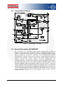
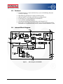
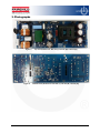
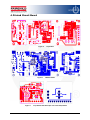
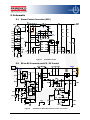
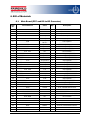
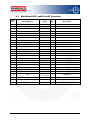
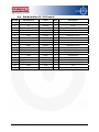
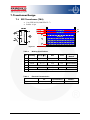
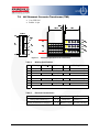
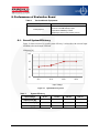
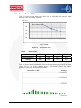
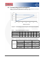
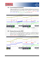
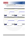
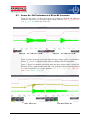
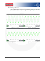
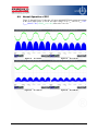
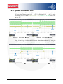
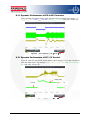
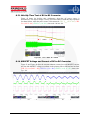
User Guide for FEBFLS1800XS1CH_L11U100A 100 W LED Driver at Universal Line Featured Fairchild Products: FL7930B, FLS1800XS Direct questions or comments about this evaluation board to: “Worldwide Direct Support” Fairchild Semiconductor.com © 2012 Fairchild Semiconductor Corporation 1 FEBFLS1800XS1CH_L11U100A • Rev. 1.0.0 Table of Contents 1. Introduction ............................................................................................................................................ 3 1.1. General Description of FL7390B ................................................................................................. 3 1.2. Features......................................................................................................................................... 3 1.3. Internal Block Diagram ................................................................................................................ 4 1.4. General Description of FLS1800XS ............................................................................................. 4 1.5. Features......................................................................................................................................... 5 1.6. Internal Block Diagram ................................................................................................................ 5 2. Specifications for Evaluation Board ....................................................................................................... 6 3. Photographs ............................................................................................................................................ 7 4. Printed Circuit Board.............................................................................................................................. 8 5. Schematic ............................................................................................................................................... 9 5.1. Power Factor Correction (PFC) .................................................................................................... 9 5.2. DC-to-DC Converter and CC / CV Control ................................................................................. 9 6. Bill of Materials.................................................................................................................................... 10 6.1. Main Board (PFC and DC-to-DC Converter) ............................................................................. 10 6.2. Sub Board for CC / CV Control ................................................................................................. 12 7. Transformer Design .............................................................................................................................. 13 7.1. PFC Transformer (TM1) ............................................................................................................ 13 7.2. LLC Resonant Converter Transformer (TM2) ........................................................................... 14 8. Performance of Evaluation Board ........................................................................................................ 15 8.1. Overall System Efficiency .......................................................................................................... 15 8.2. Power Factor (PF) ....................................................................................................................... 16 8.3. Constant Voltage and Current Regulation .................................................................................. 17 8.4. Overall Startup Performance ...................................................................................................... 18 8.5. Startup Performance of PFC ....................................................................................................... 18 8.6. Soft-Start Performance of PFC ................................................................................................... 19 8.7. Power On / Off Performance of DC-to-DC Converter ............................................................... 20 8.8. AC Input Current ........................................................................................................................ 21 8.9. Normal Operation of PFC........................................................................................................... 22 8.10. Dynamic Performance of PFC .................................................................................................... 23 8.11. Dynamic Performance of DC-to-DC Converter ......................................................................... 24 8.12. Dynamic Performance of CC / CV Control ................................................................................ 24 8.13. Hold-Up Time Test of DC-to-DC Converter.............................................................................. 25 8.14. MOSFET Voltage and Current of DC-to-DC Converter ............................................................ 25 8.15. Secondary-Side Rectifier Diode Voltage and Current ................................................................ 26 8.16. Operating Temperature ............................................................................................................... 27 9. Revision History ................................................................................................................................... 28 © 2012 Fairchild Semiconductor Corporation 2 FEBFLS1800XS1CH_L11U100A • Rev. 1.0.0 This user guide supports the evaluation kit for the FL7930B and FLS1800XS (orderable as FEBFLS1800XS1CH_L11U100A). It should be used in conjunction with the FL7930B and FLS1800XS datasheets as well as Fairchild’s application notes and technical support team. Please visit Fairchild’s website at www.fairchildsemi.com. 1. Introduction This document describes a proposed solution for an 100 W LED ballast, which consists of a boost converter for power factor correction (PFC), DC-DC converter with LLC resonant converter, and LED-current and voltage-regulation circuitry. The input voltage range is 90 VRMS – 265 VRMS and there is one DC output with a constant current of 1.0 A at 100 VMAX. The power supply mainly utilizes Fairchild semiconductor components: FL7930B CRM PFC controller, FLS1800XS half-bridge LLC controller with power MOSFET, LM2904 op-amp for LED current and voltage control, FDPF12N60NZ UniFET™ technology N-channel MOSFET, and FFPF08H60S “hyperfast” 2 rectifier. This document contains important information (e.g. schematic, bill of materials, printed circuit layout, and transformer design documentation) and the typical operating characteristics. 1.1. General Description of FL7390B The FL7930B is an active Power Factor Correction (PFC) controller for low- and highpower lumens applications that operate in Critical Conduction Mode (CRM). It uses a voltage-mode PWM that compares an internal ramp signal with the error amplifier output to generate a MOSFET turn-off signal. Because the Voltage-Mode CRM PFC controller does not need rectified AC line voltage information, it saves the power loss of an input voltage-sensing network necessary for a Current-Mode CRM PFC controller. FL7930 provides over-voltage, open-feedback, over-current, input-voltage-absent detection, and under-voltage lockout protections. The FL7930B can be disabled if the INV pin voltage is lower than 0.45 V and the operating current decreases to a very low level. Using a new variable on-time control method, Total Harmonic Distortion (THD) is lower than the conventional CRM boost PFC ICs. The FL7930B provides an additional OVP pin that can be used to shutdown the boost power stage when output voltage exceeds OVP level due to damaged resistors connected at the INV pin. 1.2. Features Low Total Harmonic Distortion (THD) Precise Adjustable Output Over-Voltage Protection (OVP) Open-Feedback Protection and Disable Function Zero Current Detector (ZCD) 150 μs Internal Startup Timer MOSFET Over-Current Protection (OCP) Under-Voltage Lockout with 3.5 V Hysteresis (UVLO) Low Startup (40 μA) and Operating Current (1.5 mA) Totem-Pole Output with High-State Clamp +500 / -800 mA Peak Gate Drive Current SOP-8 Packaging © 2012 Fairchild Semiconductor Corporation 3 FEBFLS1800XS1CH_L11U100A • Rev. 1.0.0 1.3. Internal Block Diagram Figure 1. 1.4. Block Diagram of FL7930B General Description of FLS1800XS The FLS1800XS power controller includes highly integrated power switches for medium- to high-power lumens applications. Offering everything necessary to build a reliable and robust half-bridge resonant converter, the FLS1800XS simplifies designs, improves productivity, and improves performance. The FLS1800XS series combines power MOSFETs with fast-recovery type body diodes, a high-side gate-drive circuit, an accurate current-controlled oscillator, frequency-limit circuit, soft-start, and built-in protection functions. The high-side gate-drive circuit has common-mode noisecancellation capability, which guarantees stable operation with excellent noise immunity. The fast-recovery body diode of the MOSFETs improves reliability against abnormal operation conditions, while minimizing the effects of reverse recovery. Using ZeroVoltage Switching (ZVS) dramatically reduces the switching losses and significantly improves efficiency. ZVS also reduces switching noise noticeably, which enables use of a small-sized Electromagnetic Interference (EMI) filter. The FLS1800XS can be applied to resonant converter topologies such as series resonant, parallel resonant, and LLC resonant converters. © 2012 Fairchild Semiconductor Corporation 4 FEBFLS1800XS1CH_L11U100A • Rev. 1.0.0 1.5. Features 1.6. Variable Frequency Control with 50% Duty Cycle for Half-Bridge Resonant Converter Topology High Efficiency through Zero-Voltage Switching (ZVS) Internal UniFET™ (0.95 Ω) with Fast-Recovery Body Diode Fixed Dead Time (350 ns) Optimized for MOSFETs Up to 300 kHz Operating Frequency Auto-Restart Operation for All Protections with External LVCC Protections: Over-Voltage Protection (OVP), Over-Current Protection (OCP), Abnormal Over-Current Protection (AOCP), Internal Thermal Shutdown (TSD) Internal Block Diagram Figure 2. © 2012 Fairchild Semiconductor Corporation Block Diagram of FLS1800XS 5 FEBFLS1800XS1CH_L11U100A • Rev. 1.0.0 2. Specifications for Evaluation Board Table 1. Specifications for LED Lighting Lamp Description Input Output Symbol Value Comments VIN.MIN 90 V Minimum Input Voltage VIN.MAX 265 V Maximum Input Voltage VIN.NOMINAL 110 V / 220 V Nominal Input Voltage Frequency fIN 60 Hz / 50 Hz Line Frequency Voltage VOUT 100 V Nominal Output Voltage IOUT 1A Nominal Output Current CC Deviation < 0.79% Line & Load Regulation Voltage Current Efficiency PF / THD Eff85VAC 91.73% Efficiency at 85 VAC Line Input Voltage Eff115VAC 92.55% Efficiency at 115 VAC Line Input Voltage Eff235VAC 95.01% Efficiency at 235 VAC Line Input Voltage Eff265VAC 95.11% Efficiency at 265 VAC Line Input Voltage PF/THD85VAC 0.986 / 12.56% PF/THD at 85 VAC Line Input Voltage PF/THD115VAC 0.989 / 12.01% PF/THD at 115 VAC Line Input Voltage PF/THD235VAC 0.930 / 9.8% PF/THD at 235 VAC Line Input Voltage PF/THD265VAC 0.891 / 15.47% PF/THD at 265 VAC Line Input Voltage All data of the evaluation board was measured with the board enclosed in a case and external temperature of around 25°C. © 2012 Fairchild Semiconductor Corporation 6 FEBFLS1800XS1CH_L11U100A • Rev. 1.0.0 3. Photographs Figure 3. Figure 4. Top View (Dimensions: 225 mm (L) x 80 mm (W) x 30 mm (H)) Bottom Views (Dimensions: 225 mm (L) x 80 mm (W) x 30 mm (H)) © 2012 Fairchild Semiconductor Corporation 7 FEBFLS1800XS1CH_L11U100A • Rev. 1.0.0 4. Printed Circuit Board Figure 5. Top Pattern Figure 6. Figure 7. © 2012 Fairchild Semiconductor Corporation Bottom Pattern Top / Bottom Sub Board (CC / CV Contol Part) Pattern 8 FEBFLS1800XS1CH_L11U100A • Rev. 1.0.0 5. Schematic 5.1. Power Factor Correction (PFC) Figure 8. Schematic for PFC 5.2. DC-to-DC Converter and CC / CV Control Figure 9. © 2012 Fairchild Semiconductor Corporation Schematic for DC-to-DC Converter and CC / CV Control 9 FEBFLS1800XS1CH_L11U100A • Rev. 1.0.0 6. Bill of Materials 6.1. Main Board (PFC and DC-to-DC Converter) Item No. Part Reference Value Qty. Description 1 U101 FL7930B 1 8-SOP, Fairchild Semiconductor 2 U102 FLS1800XS 1 9-SIP, Fairchild Semiconductor 3 PC101 PC817 1 Opto-Coupler, Fairchild Semiconductor 4 C101, C102, C103 0.47 µF 3 X - Capacitor 5 C104, C105 4700 pF 2 Y - Capacitor 6 C106 0.68 µF / 630 VAC 1 Film Capacitor 7 C107, C108 120 µF / 450 V 2 Electrolytic Capacitor 8 C109 22 µF / 50 V 1 Electrolytic Capacitor 5 Electrolytic Capacitor 9 C110, C112 C204, C205, C206 33 µF / 50 V 10 C111, C113 NC 11 C114 10 µF / 16 V 12 C115 0.33 µF / 25 V 1 Electrolytic Capacitor 13 C116 3.3 nF 1 AC Ceramic Capacitor 14 C117 0.1 µF / 50 V 1 Chip Capacitor 15 C118 470 pF 1 Chip Capacitor 16 C119, C124 0.22 µF 2 Chip Capacitor 17 C120 47 nF 1 Chip Capacitor 18 C121, C122 1 nF 2 Chip Capacitor 19 C123 15 nF / 630 V 1 Film Capacitor 20 C125 100 pF 1 Chip Capacitor 21 C126 680 pF 1 Chip Capacitor 22 C127 12 nF 1 Chip Capacitor 23 C201, C202, C203 100 µF / 200 V 3 Electrolytic Capacitor 24 D101 D15XB60 1 Shindengen/Bridge Diode 25 D102, D201, D202 FFPF08H60S 3 Fairchild Semiconductor No Connection 1 Electrolytic Capacitor 26 D103 1N4148 1 LL-34, Fairchild Semiconductor 27 D104, D109, D110, D203 UF4007 4 Fairchild Semiconductor 28 D105, D204 1N4745 2 Fairchild Semiconductor 29 D107 1N4736 1 Fairchild Semiconductor 30 D106, D108 NC 31 Q101 FDPF12N60NZ 1 Fairchild Semiconductor 33 Q102, Q103, U201 Q2N2222A 3 SOT-23, Fairchild Semiconductor 34 Q105 2N2222A 1 TO-92, Fairchild Semiconductor 35 Q104 2N2907 1 SOT-23, Fairchild Semiconductor 36 R101, R102, R103, R128, R129 1 MΩ-J 5 SMD Resistor, 3216 37 R104, R105 69 kΩ 2 2W © 2012 Fairchild Semiconductor Corporation 10 No Connection FEBFLS1800XS1CH_L11U100A • Rev. 1.0.0 6.1. Main Board (PFC and DC-to-DC Converter) Item No. Part Reference Value Qty. Description 38 R106 0.1 Ω 1 5W 39 R107 47 Ω-J 1 SMD Resistor, 3216 40 R108 4.7 Ω -J 1 SMD Resistor, 3216 41 R109, R119, R131, R132, R203 10 kΩ-J 5 SMD Resistor, 3216 42 R110, R111, R112, R114, R115, R116 3.9 MΩ-J 6 SMD Resistor, 3216 43 R113 75 kΩ-J 1 SMD Resistor, 3216 44 R117 68 kΩ-J 1 SMD Resistor, 3216 45 R118 24 kΩ-J 1 SMD Resistor, 3216 46 R120, R133, R201 5.1 Ω-J 3 SMD Resistor, 3216 47 R121 33 kΩ-J 1 SMD Resistor, 2012 48 R122, R202 100 kΩ-J 2 SMD Resistor, 2012 49 R123 390 kΩ-J 1 SMD Resistor, 2012 50 R124, R125 NC Optional 51 R126 0.1 Ω 1 1W 52 R127 1 kΩ-J 1 SMD Resistor, 2012 53 R130 47 kΩ-J 1 SMD Resistor, 2012 54 R134 2.7 Ω-J 1 SMD Resistor, 2012 55 R135 5.6 kΩ-J 1 SMD Resistor, 2012 56 R136 2 kΩ-J 1 SMD Resistor, 2012 57 TH1, TH2 5D15 2 NTC 58 ZNR1, ZNR2 10D471 2 Varistor 59 TM1 280 µH 1 EER3019N-10 60 TM2 Lp = 850 µH LR = 170 µH 1 EER3543-16 61 LF101, LF102 40 mH 2 Line Filter 62 F1 250 V / 5 A 1 Fuse 63 J101 NC © 2012 Fairchild Semiconductor Corporation 11 Optional FEBFLS1800XS1CH_L11U100A • Rev. 1.0.0 6.2. Sub Board for CC / CV Control Item No. Part Reference Value Qty. Description 1 U9 2 U11 KA431SLMF 1 SOT-23, Fairchild Semiconductor LM2904 1 8-SOP 3 RS33 47 kΩ-J 1 SMD Resistor, 3216 4 5 RS35 13 kΩ-J 1 SMD Resistor, 3216 RS40 100 kΩ-J 1 SMD Resistor, 3216 6 RS41 4.7 kΩ-J 1 SMD Resistor, 3216 7 RS49 1 kΩ-J 1 SMD Resistor, 3216 8 RS55 120 kΩ-J 1 SMD Resistor, 3216 9 RS56 47 kΩ-J 1 SMD Resistor, 3216 10 RS57 330 kΩ-J 1 SMD Resistor, 3216 11 RS59 8.2 kΩ-J 1 SMD Resistor, 3216 12 RS60 3 Ω-J 1 SMD Resistor, 2012 13 CS19 220 nF 1 Chip Capacitor 14 CS25 220 nF 1 Chip Capacitor 15 CS22 10 µF / 25 V 1 Electrolytic Capacitor 16 DS3, DS5 1N4148 2 LL-34, Fairchild Semiconductor 17 RS42 NC 18 RS44 0.1 Ω 19 RS46 NC © 2012 Fairchild Semiconductor Corporation No Connection 1 2W No Connection 12 FEBFLS1800XS1CH_L11U100A • Rev. 1.0.0 7. Transformer Design 7.1. PFC Transformer (TM1) Core: EER3019N (SAMHWA PL-7) Bobbin: 10 pin Figure 10. Table 2. Transformer Specifications & Construction Winding Specifications No. Winding Pin (S F) Wire Turns Winding Method 1 Np 3, 4 → 1, 2 0.1φ × 50 39 Ts Solenoid Winding 2 Insulation: Polyester Tape t = 0.025 mm, 3-Layer 3 NauxA 4 10 → 9 0.3φ 5 Ts Solenoid Winding Insulation: Polyester Tape t = 0.025 mm, 3-Layer 5 NauxB 6 6→ 7 0.3φ 5 Ts Solenoid Winding Insulation: Polyester Tape t = 0.025 mm, 3-Layer Table 3. Electrical Characteristics Inductance © 2012 Fairchild Semiconductor Corporation Pin Specifications Remark 3, 4 – 1, 2 280 µH ±5% 100 kHz, 1 V 13 FEBFLS1800XS1CH_L11U100A • Rev. 1.0.0 7.2. LLC Resonant Converter Transformer (TM2) Core: EER3543 Bobbin: 16 pin Figure 11. Table 4. Transformer Specifications & Construction Winding Specifications No Winding 1 Np 2 Pin (S F) Wire Turns Winding Method 8→2 0.1φ × 20 38 Ts Solenoid Winding Insulation: Polyester Tape t = 0.025 mm, 3-Layer 3 Ns1 4 10 → 9 0.3φ 2 Ts Solenoid Winding Insulation: Polyester Tape t = 0.025 mm, 3-Layer 5 Ns2 6 13 → 11 0.1φ×20 17 Ts Solenoid Winding Insulation: Polyester Tape t = 0.025 mm, 3-Layer 7 Ns3 8 16 → 14 0.1φ×10 17Ts Center Solenoid Winding Insulation: Polyester Tape t = 0.025 mm, 3-Layer Table 5. Electrical Characteristics Primary-Side Inductance (Lp) Primary-Side Effective Leakage (LR) © 2012 Fairchild Semiconductor Corporation 14 Pin Specification 2–8 850 µH ±5% 2–8 Remark 100 KHz, 1 V Short One of the Maximum 170 µH Secondary Windings FEBFLS1800XS1CH_L11U100A • Rev. 1.0.0 8. Performance of Evaluation Board Table 6. Test Condition & Equipments TA = 25°C Ambient Temperature AC Source: ES2000S by NF Electronic Load: EML-05B by Fujitsu Power Meter: PM6000 by Voltech Oscilloscope: Wave-runner 104Xi by LeCroy Test Equipment 8.1. Overall System Efficiency Figure 12 shows at least 91% overall system efficiency is achievable with universal input condition at the rated output LED load. Efficiency [%] 100 95 90 85 85V 115V 235V 265V Input Voltage Figure 12. Table 7. System Efficiency Curve System Efficiency Input Voltage 85 VAC 115 VAC 235 VAC 265 VAC Input Power [W] 112.04 111.18 108.46 108.47 Output Power [W] 102.77 102.89 103.05 103.16 Efficiency [%] 91.73 92.55 95.01 95.11 © 2012 Fairchild Semiconductor Corporation 15 FEBFLS1800XS1CH_L11U100A • Rev. 1.0.0 8.2. Power Factor (PF) Figure 13 shows at least 89% power factor (PF) is achievable with universal input condition at the rated output LED load. PF (%) 100 95 90 85 80 85V 115V 235V 265V Input Voltage Figure 13. Table 8. Power Factor Curve Power Factor Input Voltage 85 VAC 115 VAC 235VAC 265 VAC Power Factor [%] 98.57 98.88 93.04 89.05 THD [%] 12.56 12.01 9.80 15.47 Figure 14 shows the current harmonic result at the rated output power 100 W and input voltage 230 VAC and 50 Hz condition based on IEC61000-3 class-C for lighting application. This meets international regulations. Figure 14. © 2012 Fairchild Semiconductor Corporation Total Harmonic Distortion (THD) 16 FEBFLS1800XS1CH_L11U100A • Rev. 1.0.0 8.3. Constant Voltage and Current Regulation Figure 15, Table 9, and Table 10 show the typical CC / CV performance on the board, displaying very stable CC performance over a wide input range. Output Voltage [V] 120 100 80 60 40 20 0 0.0 0.2 0.4 0.6 0.8 1.0 1.2 Output Current [A] Figure 15. Table 9. Constant Voltage and Current Regulation, Measured by E-Load [CR Mode] Output Voltage Regulation Performance Output Voltage [V] 99.300 98.678 98.348 98.135 97.819 97.604 97.460 Output Current [mA] 100 201 300 400 500 600 700 Output Voltage [V] 97.346 97.220 97.132 92.469 88.555 83.579 81.279 Output Current [mA] 798 903 1004 1012.5 1009.9 1008.1 1006.8 Table 10. Output Voltage, Current Regulation Performance in CV / CC Region CC / CV © 2012 Fairchild Semiconductor Corporation Mode CV Mode CC Mode Maximum Output 99.30 V 1.01 A Minimum Output 97.23 V 1.00 A Difference 2.07 V 0.01 A Average 98.72 V 1.01 A Deviation 2.10% 0.79% 17 FEBFLS1800XS1CH_L11U100A • Rev. 1.0.0 8.4. Overall Startup Performance Figure 16 and Figure 17 show the startup performance including boost converter, LLC resonant converter, and CV / CC circuitry. The output load current starts flowing after about 357 ms and 139 ms for input voltage of 90 VAC and 265 VAC when the AC input power switch is turned on; CH1: VCC_PFC (10 V / div), CH2: VCC_LLC (10 V / div), CH3: VCC_CC/CV (10 V / div), CH4: ILOAD (1A / div), time scale: 100 ms / div. 139 ms 357 ms Figure 16. VIN = 95 VAC Figure 17. VIN = 265 VAC 8.5. Startup Performance of PFC Figure 18 and Figure 19 show the typical startup performance on the PFC converter. It is possible to have a long startup time at 95 VAC condition rather than 265 VAC condition. This time depends on starting resistor and capacitor on board; CH1: VCC_PFC (5 V / div), CH2: VPFC (100 V / div), time scale: 100 ms / div. 354 ms Figure 18. © 2012 Fairchild Semiconductor Corporation 104 ms VIN = 95 VAC Figure 19. 18 VIN = 265 VAC FEBFLS1800XS1CH_L11U100A • Rev. 1.0.0 8.6. Soft-Start Performance of PFC Figure 20 through Figure 23 show the soft-start performance at output power of 100 W. Measured PFC output voltage reaches from 398V to 401 V at input voltage of 95 VAC and 265 VAC; CH1: VCC_PFC (10 V / div), CH3: VPFC (20 V / div), time scale: 200 ms / div. Figure 20. VIN = 95 VAC Figure 21. VIN = 115 VAC Figure 22. VIN = 235 VAC Figure 23. VIN = 265 VAC © 2012 Fairchild Semiconductor Corporation 19 FEBFLS1800XS1CH_L11U100A • Rev. 1.0.0 8.7. Power On / Off Performance of DC-to-DC Converter Figure 24 and Figure 25 show the soft-start waveforms at full-load and light-load conditions, respectively, for the nominal input voltage condition; CH2: VPFC (50 V / div), CH4: ILLC (2 A / div), time scale: 50 ms / div. Figure 24. VPFC = 400 V, PO = 100 W Figure 25. VPFC = 400 V, PO = 10 W Figure 26 shows the startup waveforms when the input voltage source is supplied first, then the VCC of 16 V is applied from the auxiliary winding of the PFC transformer. Figure 27 shows the shutdown waveforms when the input voltage source is turned off. When the DC bus voltage reaches about 260 V, the external brownout circuit disconnects VCC from FLS1800XS, so it stops operation; CH1: VCC_LLC (10 V / div), CH2: VPFC (200 V / div), CH4: ILLC (2 A / div). Figure 26. VPFC = 400 V, PO = 100 W; StartupTime Scale: 100 ms / div © 2012 Fairchild Semiconductor Corporation 20 Figure 27. VPFC = 400 V, PO = 10 W ; Shutdown Time Scale: 50 ms / div FEBFLS1800XS1CH_L11U100A • Rev. 1.0.0 8.8. AC Input Current Figure 28 through Figure 31 show the AC input current waveforms at the rated output power of 100 W and input voltage of 95 VAC, and 265 VAC; CH4: IAC (500 mA / div), time scale: 10 ms / div. Figure 28. VIN = 95 VAC Figure 29. VIN = 115 VAC Figure 30. VIN = 235 VAC Figure 31. VIN = 265 VAC © 2012 Fairchild Semiconductor Corporation 21 FEBFLS1800XS1CH_L11U100A • Rev. 1.0.0 8.9. Normal Operation of PFC Figure 32 through Figure 35 show the AC input and MOSFET drain-current waveforms at the rated output power of 100 W and input voltage of 95 VAC, and 265 VAC; CH3: ID_PFC (500 mV / div), CH4: IAC (1 A / div), time scale: 5 ms / div. Figure 32. VIN = 95 VAC Figure 33. VIN = 115 VAC Figure 34. VIN = 235 VAC Figure 35. VIN = 265 VAC © 2012 Fairchild Semiconductor Corporation 22 FEBFLS1800XS1CH_L11U100A • Rev. 1.0.0 8.10. Dynamic Performance of PFC Figure 36 and Figure 37 show the PFC output voltage changes under about 40V when the input voltage changes from 115 VAC to 235 VAC and from 235 VAC to 115 VAC at the rated output power of 100 W; CH1:VPFC (20 V / div), CH4: IAC (1 A / div), time scale: 200 ms / div. 420V 386V Figure 36. 409.8V 372.6V VIN = 115 VAC 235 VAC Figure 37. VIN = 235 VAC 115 VAC Figure 38 and Figure 39 show the PFC output voltage changes about 32 V when the output power changes from 14 W to 100 W and from 100 W to 14 W at input voltage of 235 VAC; CH1: VPFC (20 V / div), CH4: IAC (1 A / div), time scale: 100 ms / div. 407V 375.8V Figure 38. 409.4V 391.2V PO = 14 W 100 W © 2012 Fairchild Semiconductor Corporation Figure 39. 23 PO = 100 W 14 W FEBFLS1800XS1CH_L11U100A • Rev. 1.0.0 8.11. Dynamic Performance of DC-to-DC Converter Figure 40 shows the output voltage ripple with pulse load at nominal input voltage; CH1: VOUT (5 VAC / div), CH3: ILOAD (1 A / div), CH4: ILLC (1 A / div), time scale: 100 ms / div. Figure 40. VPFC = 400 V, IO = 1 A 0.1 A 1 A 8.12. Dynamic Performance of CC / CV Control Figure 41 shows the output load current and the output voltage of CC op-amp waveforms when the output load is step changed; CH1: VOPOUT_CC (2 V / div), CH4: ILOAD (500 mA / div), time scale: 500 ms / div. Steady State 140 mA Figure 41. © 2012 Fairchild Semiconductor Corporation 1A VIN = 235 VAC, IO = 0.14 A 1 A 0.14 A 24 FEBFLS1800XS1CH_L11U100A • Rev. 1.0.0 8.13. Hold-Up Time Test of DC-to-DC Converter Figure 42 shows the hold-up time performance when the AC power source is disconnected. The output voltage is slowly decreased until FLS1800XS stops operation for about 188 ms, when the power source is disconnected; CH1: VOUT (50 V / div), CH2: VPFC (200 V / div), CH4: ILLC (1 A / div), time scale: 100 ms / div. 188ms Figure 42. VPFC = 400 V, PO = 100 W 8.14. MOSFET Voltage and Current of DC-to-DC Converter Figure 43 and Figure 44 show the resonant inductor current, low-side MOSFET current, and low-side MOSFET voltage waveforms in the primary-side at full-load and no-load; CH2: VDS_LOW (200 V / div), CH3: ILLC (1 A / div), CH4: ID_LOW (1 A / div), time scale: 5 µs / div. Figure 43. VPFC = 400 V, PO = 100 W © 2012 Fairchild Semiconductor Corporation Figure 44. 25 VPFC = 400 V, PO = 0 W FEBFLS1800XS1CH_L11U100A • Rev. 1.0.0 8.15. Secondary-Side Rectifier Diode Voltage and Current Figure 45 and Figure 46 show the resonant inductor current in the primary side, rectifier diode current, and the rectifier diode voltage waveforms in the secondary side at full load. It shows the soft commutation of the rectifier diodes in the secondary side due to below resonant operation. Below resonance operation is preferred for high-output-voltage applications, such as street LED lighting systems where the reverse-recovery loss in the rectifier diode is severe; time scale: 5 µs / div. Figure 45. VPFC = 400 V, PO = 100 W; CH2: VD201 (100 V Figure 46. VPFC = 400 V, PO = 100 W; CH2: VD201 / div), CH3: ILLC (1 A / div), CH4: ID201 (1 A / div) (100 V / div), CH3: ID201 (1 A / div), CH4: ID202 (1 A / div) © 2012 Fairchild Semiconductor Corporation 26 FEBFLS1800XS1CH_L11U100A • Rev. 1.0.0 8.16. Operating Temperature Figure 47 and Figure 48 show the temperature-checking results on the board in minimum and maximum input voltage conditions at the rated LED load condition. Bottom Top Figure 47. Board Temperature - VIN = 90 VAC Top Bottom Figure 48. © 2012 Fairchild Semiconductor Corporation Board Temperature - VIN = 265 VAC 27 FEBFLS1800XS1CH_L11U100A • Rev. 1.0.0 9. Revision History Rev. Date Description 1.0.0 Nov. 2012 Initial Release WARNING AND DISCLAIMER Replace components on the Evaluation Board only with those parts shown on the parts list (or Bill of Materials) in the Users’ Guide. Contact an authorized Fairchild representative with any questions. The Evaluation board (or kit) is for demonstration purposes only and neither the Board nor this User’s Guide constitute a sales contract or create any kind of warranty, whether express or implied, as to the applications or products involved. Fairchild warrantees that its products meet Fairchild’s published specifications, but does not guarantee that its products work in any specific application. Fairchild reserves the right to make changes without notice to any products described herein to improve reliability, function, or design. Either the applicable sales contract signed by Fairchild and Buyer or, if no contract exists, Fairchild’s standard Terms and Conditions on the back of Fairchild invoices, govern the terms of sale of the products described herein. DISCLAIMER FAIRCHILD SEMICONDUCTOR RESERVES THE RIGHT TO MAKE CHANGES WITHOUT FURTHER NOTICE TO ANY PRODUCTS HEREIN TO IMPROVE RELIABILITY, FUNCTION, OR DESIGN. FAIRCHILD DOES NOT ASSUME ANY LIABILITY ARISING OUT OF THE APPLICATION OR USE OF ANY PRODUCT OR CIRCUIT DESCRIBED HEREIN; NEITHER DOES IT CONVEY ANY LICENSE UNDER ITS PATENT RIGHTS, NOR THE RIGHTS OF OTHERS. LIFE SUPPORT POLICY FAIRCHILD’S PRODUCTS ARE NOT AUTHORIZED FOR USE AS CRITICAL COMPONENTS IN LIFE SUPPORT DEVICES OR SYSTEMS WITHOUT THE EXPRESS WRITTEN APPROVAL OF THE PRESIDENT OF FAIRCHILD SEMICONDUCTOR CORPORATION. As used herein: 1. Life support devices or systems are devices or systems which, (a) are intended for surgical implant into the body, or (b) support or sustain life, or (c) whose failure to perform when properly used in accordance with instructions for use provided in the labeling, can be reasonably expected to result in significant injury to the user. 2. A critical component is any component of a life support device or system whose failure to perform can be reasonably expected to cause the failure of the life support device or system, or to affect its safety or effectiveness. ANTI-COUNTERFEITING POLICY Fairchild Semiconductor Corporation's Anti-Counterfeiting Policy. Fairchild's Anti-Counterfeiting Policy is also stated on our external website, www.fairchildsemi.com, under Sales Support. Counterfeiting of semiconductor parts is a growing problem in the industry. All manufacturers of semiconductor products are experiencing counterfeiting of their parts. Customers who inadvertently purchase counterfeit parts experience many problems such as loss of brand reputation, substandard performance, failed applications, and increased cost of production and manufacturing delays. Fairchild is taking strong measures to protect ourselves and our customers from the proliferation of counterfeit parts. Fairchild strongly encourages customers to purchase Fairchild parts either directly from Fairchild or from Authorized Fairchild Distributors who are listed by country on our web page cited above. Products customers buy either from Fairchild directly or from Authorized Fairchild Distributors are genuine parts, have full traceability, meet Fairchild's quality standards for handling and storage and provide access to Fairchild's full range of up-to-date technical and product information. Fairchild and our Authorized Distributors will stand behind all warranties and will appropriately address any warranty issues that may arise. Fairchild will not provide any warranty coverage or other assistance for parts bought from Unauthorized Sources. Fairchild is committed to combat this global problem and encourage our customers to do their part in stopping this practice by buying direct or from authorized distributors. © 2012 Fairchild Semiconductor Corporation 28 FEBFLS1800XS1CH_L11U100A • Rev. 1.0.0