1
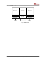
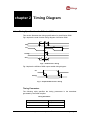
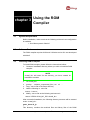
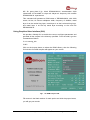
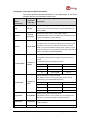
VeriSilicon GSMC 0.15μm Low-Power Synchronous Diffusion ROM Compiler User’s Guide Trademark Acknowledgments VeriSilicon & the VeriSilicon logo are the trademarks of VeriSilicon Microelectronics (Shanghai) Co., Ltd. All other products and company names mentioned may be the trademarks of their respective owners. © 2002 VeriSilicon Microelectronics (Shanghai) Co., Ltd. All rights reserved. Printed in P.R.China. VeriSilicon Microelectronics (Shanghai) Co., Ltd. reserves all its copy rights and other intellectual property rights, ownership, powers, benefits and rights arising or to arise from this manual. All or part of the contents of this manual may be changed by VeriSilicon Microelectronics (Shanghai) Co., Ltd. without notice at any time for any reason, including but not limited to improvement of the product relating hereto. VeriSilicon Microelectronics (Shanghai) Co., Ltd. shall not undertake or assume any obligation, responsibility or liability arising out of or in respect of the application or use of the product described herein, except for reasonable, careful and normal uses. Nothing, whether in whole or in part, within this manual can be reproduced, duplicated, copied, changed or disposed of in any form or by any means without prior written consent by VeriSilicon Microelectronics (Shanghai) Co., Ltd.. VeriSilicon Microelectronics (Shanghai) Co., Ltd. 3F, Building 1, No.200, Zhangheng Road, Zhangjiang Hi-Tech Park, Pudong New Area, Shanghai 201204, P. R. China Tel : +86-21-5131-1118 Fax : +86-21-5131-1119 Web : http://www.verisilicon.com 3 Contents Chapter 1 Introduction 1.1 1.2 1.3 1.4 1.5 1.6 4 Compiler Description..................................................4 Features.....................................................................4 Operating Conditions .................................................4 Pin Descriptions .........................................................5 Parameter Range.......................................................5 ROM Floor Plan .........................................................6 Chapter 2 Timing Diagram 7 2.1 Timing Specifications for Diffusion ROM....................7 Timing Parameters ........................................7 Power Parameters.........................................8 Chapter 3 Using the ROM Compiler 9 3.1 3.2 3.3 3.4 3.5 System Requirement .................................................9 Software Environment................................................9 Installing ROM Compiler ............................................9 Inputs and Outputs...................................................10 Getting Started.........................................................11 Using Shell Commands...............................11 Using Graphical User Interface (GUI)..........12 3.6 Generating the Outputs............................................14 VeriSilicon GSMC 0.15um LP Syn. DROM Compiler User’s Guide Introduction 4 chapter 1 Introduction 1.1 Compiler Description VeriSilicon GSMC 0.15μm Low-Power Synchronous Diffusion ROM compiler optimized for Grace Semiconductor Manufacturing Corporation (GSMC) 0.15μm Logic 1P7M Salicide 1.5/3.3V process can flexibly generate memory blocks via a friendly GUI or shell commands. The compiler supports a comprehensive range of word lengths and bit lengths. While satisfying speed and power requirements, it is optimized for area efficiency. VeriSilicon GSMC 0.15μm Low-Power Synchronous Diffusion ROM compiler uses three metal layers within the blocks and supports metal 4, 5, 6 or 7 as the top metal. Dummy bit cells are embedded with the intention to enhance reliability. 1.2 Features • High Density • High Speed • Size Sensitive Self-time Delay for Fast Access and "Zero" Hold Time • Automatic Power Down 1.3 Operating Conditions The following table gives the recommended operating conditions for memory blocks generated by ROM compiler: Operating Conditions Parameter Rating Supply Voltage 1.5V 1.35V to 1.65V Temperature 25ºC 0ºC to 125ºC VeriSilicon GSMC 0.15um LP Syn. DROM Compiler User’s Guide Introduction 5 1.4 Pin Descriptions The following table gives detailed information of pin descriptions for ROM (Bus index in descending order): 1.5 Pin Description DOUT[i] Data output AD[i] Address input CEN Chip enable input, low enable CLK CLK input, positive edge active OE Output enable, high enable Parameter Range Parameter Range Memory Array Range 128 to 2M Bits Data Width 2 to 128 Bits, Increments of 1 ROM Address Depth 64 to 32768 Words, Increments of (8 X Column Mux) The following list shows the changes of width and height when column mux is set to different values. Suppose when column mux is 16, the width and height are standard. Width Height 8 1/2 2 16 1 1 32 2 1/2 Column Mux Top Metal Output Drive Strength m4, m5, m6 or m7 The same drive as INVHD8X cell in VeriSilicon GSMC 0.15μm High-Density Standard Cell Library VeriSilicon GSMC 0.15um LP Syn. DROM Compiler User’s Guide Introduction 6 1.6 ROM Floor Plan Memory Array Row decoder Column Decoder Memory Array Column Decoder CLK control Sense Amplifier Sense Amplifier CLK&CEN&AD&OE Data Output Data Output Fig.1 ROM Floor Plan VeriSilicon GSMC 0.15um LP Syn. DROM Compiler User’s Guide Introduction 7 chapter 2 Timing Diagram 2.1 Timing Specifications for Diffusion ROM This section illustrates the timing specifications for the diffusion ROM. Fig.2 depicts the read function timing diagram of diffusion ROM. tas tah AD[i] tcyc CLK ta DOUT[i] tcs CEN Fig.2 tch Read-Function Timing Fig.3 depicts the diffusion ROM output enable timing diagram: OE tlz thz DOUT[i] Fig.3 Output-Enable Function Timing Timing Parameters The following table specifies the timing parameters in the datasheet generated by the ROM compiler: Timing Parameters Parameter Symbol Cycle time tcyc Access time* ta VeriSilicon GSMC 0.15um LP Syn. DROM Compiler User’s Guide Timing Diagram 8 Address setup time tas Address hold time tah Chip enable setup time tcs Chip enable hold time tch Output enable to hi-Z time tlz Output enable active time* thz * Parameters values are loaded dependently. Power Parameters The following table specifies the power parameters in the datasheet generated by the ROM compiler: Power Parameters Parameter Symbol Average current Iavg Peak current Ipeak iavg is the average current in A/100MHz unit. The average current in the datasheet is achieved under below assumptions: 1. Input net transition is 0.2ns. 2. Output port capacitance is 0pF. The total average current of the memory than can be estimated according to the following equation: Iavg = iavg * F + 1/2 * C * V * f * N Where, Iavg: the total average current of the memory. (A) F: the frequency of clock. (100MHz) C: the average capacitance of output port. (F) V: the voltage supply. (V) f: the frequency of output port. (Hz) N: switched ports number. ipeak is the peak current of memory during operation in A unit. VeriSilicon GSMC 0.15um LP Syn. DROM Compiler User’s Guide Timing Diagram 9 Using the ROM chapter 3 Compiler 3.1 System Requirement Before installation, make sure that the following minimum host configuration is available: • Sun Microsystem's Solaris7 3.2 Software Environment The ROM compiler requires UNIX and X-Window as its GUI was developed with Motif. 3.3 Installing ROM Compiler To install ROM compiler, please follow the instructions bellow: 1. Create an installation directory where you wish to install the ROM compiler. NOTE <install_dir> will stand for the directory you have created for installation hereafter. 2. 3. 4. 5. cd <install_dir> gunzip < <release_compressed_file> | tar Copy .vsmcrc file to the home directory. Add the following to .cshrc file. xvf - source ~/.vsmcrc 6. Modify .vsmcrc file as the following and source it: setenv VERISILICON_MC_DIR <install_dir> After successful installation, the following directory structure will be created under <install_dir>: gsmc_drom.15_lp This directory contains the technical files and library files of the ROM VeriSilicon GSMC 0.15um LP Syn. DROM Compiler User’s Guide Using the ROM Compiler 10 compiler. The following table lists the names of the executable files in the installation directory and its description: Name Description MC The executable file of ROM compiler. NOTE Be sure not to edit any files in <install_dir> directory. 3.4 Inputs and Outputs The ROM compiler allows users to define the following input parameters for a specific ROM block: Library Running Directory Block Name Number of Words Number of Bits Ring Width Frequency (MHz) ROM Code File Multiplexer Width Horizontal Ring Layer Vertical Ring Layer Top Metal Layer The ROM compiler generates the following output files. GDSII Layout File ( GDSII format ) LVS Netlist ( CDL format ) Verilog Model Code TLF Timing Synopsys Model Datasheet ROM code file LEF view Antenna LEF view VeriSilicon GSMC 0.15um LP Syn. DROM Compiler User’s Guide Using the ROM Compiler 11 Antenna CLF model After inputting the parameters, users should wait a few minutes for the outputs to be generated by the ROM compiler automatically. 3.5 Getting Started There are two ways to start ROM compiler as follows: Using Shell Commands Users can launch ROM compiler using commands line in the shell window. Enter the following commands to launch the ROM compiler directly from the shell: % cd <running_dir> % MC [options with parameters] The <running_dir> is the directory in which the ROM compiler runs. All the outputs will be generated in this directory. Make sure that the running directory < running_dir> is different from the installation directory <install_dir>. The following options can be specified in the command line: -lib $lib_dir -outdir $run_dir -block $mem_name -wordsnumber $memlength -bitsnumber $datawidth -ringwidth $ringwidth -muxwidth $varMuxWidth -vlayer $varVLayer -hlayer $varHLayer -frequency $frequency -codefile $codefile -topmetal $topmetal -area y/n Please see section Parameters under GUI and Shell Commands for detailed explanation. Example: VeriSilicon GSMC 0.15um LP Syn. DROM Compiler User’s Guide Using the ROM Compiler 12 MC -lib gsmc_drom.15_lp -block DROM2048X16 -wordsnumber 2048 -bitsnumber 16 -muxwidth 16 -vlayer m3 -hlayer m4 -frequency 100 -codefile DROM2048X16 -topmetal m4 This command will generate a ROM name of DROM2048X16, with 2048 words, 16 bits, 16 column multiplexer width, frequency of 100MHz, metal layer 3 as the vertical ring layer, metal layer 4 as the horizontal ring layer, and metal layer 4 as the top metal layer according to the code file DROM2048X16. Using Graphical User Interface (GUI) We provide a friendly GUI to enable the users to configure parameters and generate all the outputs in the directory specified. From the shell, type the commands as follows: % cd <running_dir> % MC Click on the browse button to select the ROM’s library, then the following GUI window for ROM compiler will appear on your screen: Fig.1 the ROM Compiler GUI Fill content in the blank textbox for each option and click the proper button, you will get your results. VeriSilicon GSMC 0.15um LP Syn. DROM Compiler User’s Guide Using the ROM Compiler 13 Parameters under GUI and Shell Commands The section specifies detailed descriptions of the parameters of the ROM compiler and their corresponding default value: Parameter under Shell Commands Parameter under GUI Description Specify the library directory used by the Register File compiler. -lib Library You can click on the browse button to find the valid library you have installed. -rundir Running Directory Specify the output directory of the ROM compiler. The directory name can be any valid path name supported by the system. The default is current directory. Specify the block name. The block name can include any alphanumeric value and must -block Block Name be unique to avoid name conflicts for blocks within the same library. It is recommended that a block name contains no more than 16 characters, for we will identify two blocks by their first 16 letters. The default is DROM4096X32M8. Specify the number of words in the block. The default value is 4096. The range for words can be 64 to 32768. -wordsnumber Number of The following gives the detailed information: Words Mux Number of words Increment 8 64 to 8192 Mux * 8 16 128 to 16384 Mux * 8 32 256 to 32768 Mux * 8 Specify the number of bits in the block. The default value is 32. The range for bits can be 2 to 128. The following gives the detailed information: -bitsnumber Number of Bits Mux Number of Bits Increment 8 2 to 128 1 16 2 to 128 1 32 2 to 64 1 Specify the ring width of the block in um. -ringwidth Ring Width The default value is 5. The minimum is 2. The designer must decide the ring width according to the power analysis. -frequency Frequency -codefile CodeFile Specify the frequency of the clock of the chip in MHz. The default value is 100MHz. Specify the code file of the ROM. Please refer to the following VeriSilicon GSMC 0.15um LP Syn. DROM Compiler User’s Guide Using the ROM Compiler 14 figure for detailed information about the code file format. If an user doesn’t specify the code file or the code file he specifies doesn’t exist, all the bits of the ROM block will be set to 1 automatically. The default is NOCODE. Specify the column multiplexer width. -muxwidth Multiplexer Width The default value is 8. There are three buttons for your choice: 8, 16, or 32. When this option is set to different values, the width and height of the block will change correspondingly. For detailed information, please refer to Parameter Range section on page 5. -vlayer -hlayer -topmetal -area Vertical Specify which metal layer will be the vertical ring layer. It can Ring Layer only be m4. Horizontal Specify which metal layer will be the horizontal ring layer. It can Ring Layer only be m3. Top Metal Specify the top metal layer. It can be m4, m5 or m6. The default Layer value is m4. y/n Once “–area y” is used, the compiler will only generate a width X height report. Default is n. The following illustrates the format of code file of a ROM name of DROM64 ×7, with 64 words, 7 bits: Column 1 = bit 6 (the highest bit) Column 7 = bit 0 1010001 (the lowest bit) 1111111 Line 1 = address 0 0000000 · · · Line 64 = address 63 0011110 1100111 Each character in a line indicates the bit of a word. 3.6 Generating the Outputs When you click on the Default button in the GUI window, the ROM compiler will automatically load the default parameters of the ROM and generate the ROM based on the default parameters. To generate the outputs, click on Generate button. All the outputs are generated according to the generic parameters you set and are placed in the VeriSilicon GSMC 0.15um LP Syn. DROM Compiler User’s Guide Using the ROM Compiler 15 user specified running directory <running_dir>. The following table lists the detailed description of the output files: Name Description *.tlf TLF Model *.lib Synopsys Model *.net Cdl netlist *.gds GDS file *.ds Datasheet *.v Verilog Model *.dat Rom Code File *.lef LEF view *_antenna.lef Antenna LEF view *_antenna.clf Antenna CLF model And click on Exit button to quit the ROM compiler. VeriSilicon GSMC 0.15um LP Syn. DROM Compiler User’s Guide Using the ROM Compiler