1
PATI
User Manual
High-Tech • Made in Switzerland
PATI
PowerPC controlled Analog and Timing I/O Intelligence
The PATI is a highly integrated I/O board in PC/104 form factor. Build around the MPC555 Motorola
PowerPC™ Processor and the PLX9056 PCI Bridge it brings the superb MPC555 peripherals to a standard
PCI interface.
With the possibilities for firmware update over the PCI bus, parameter passing via the on-board SDRAM,
allowing the PATI to access the host memory via PCI busmaster access and various configurations options it is
well suited for fast prototyping application.
A stand-alone mode allows the PATI to work without the host. Application developed and tested in a host
environment can be executed on the PATI in the stand-alone mode without any code modification.
The MPC555 peripherals are available on 2 standard 50 pin 2.54mm header, which offers easy connections. It
features 8 differential 10bit Analog/Digital channels, 32Bit TPU channels, 2 serial Interfaces and 2 CAN
interfaces.
● Features:
• Motorola MPC555 PowerPC™ Processor
• 40MHz Processor Clock
• 16MByte SDRAM on-board
• up to 8MByte on-board Flash
• 32Bit 33MHz PCI Agent Interface
• Bus Master capable
• Low power consumption
• 5V only Power Supply
• 8 differentials 10bit Analog/Digital converter channels
• 32Bit TPU channels
• 2 Serial Interface
• 2 CAN Interface
2009 by MPL AG
1
MEH-10102-001 Rev. D
PATI
User Manual
High-Tech • Made in Switzerland
TABLE OF CONTENTS
1 INTRODUCTION.............................................................................................................5
1.1 ABOUT THIS MANUAL.........................................................................................................5
1.2 SAFTY PRECAUTIONS AND HANDLING............................................................................5
1.3 ELECTROSTATIC DISCHARGE (ESD) PROTECTION........................................................5
1.4 EQUIPMENT SAFETY...........................................................................................................5
1.5 MANUAL REVISIONS............................................................................................................6
1.5.1 RELATED PRODUCTS..................................................................................................6
1.5.2 REVISION HISTORY.....................................................................................................6
1.6 RELATED DOCUMENTATION..............................................................................................7
1.7 ORDERING INFORMATION..................................................................................................7
2 SPECIFICATIONS...........................................................................................................8
3 PARTS LOCATION.........................................................................................................9
3.1 Connectors..........................................................................................................................10
3.1.1 J1 Analog Input and CAN Connector............................................................................10
3.1.2 J2 JTAG Connector......................................................................................................10
3.1.3 J3 - PC104+ Interface pin numbers..............................................................................11
3.1.4 J4 TPU and Serial Connector.......................................................................................12
3.1.5 J5 - Power Connector...................................................................................................12
3.1.6 J6 - Debug Connector..................................................................................................13
3.1.7 J7/8 - PC104 interface pin numbers.............................................................................13
3.2 Switch..................................................................................................................................14
3.2.1 DIP switch S1 –Configuration switch............................................................................14
4 OPERATION.................................................................................................................15
4.1 Block Schematic.................................................................................................................15
4.2 Mapping Overview..............................................................................................................16
4.3 Used Environment..............................................................................................................17
4.4 Local Memory Map.............................................................................................................17
4.5 PCI Memory Map.................................................................................................................18
4.5.1 PCI Bridge Local Bus Memory Mapping.......................................................................18
4.5.2 PCI Bridge PCI Memory Map.......................................................................................18
4.5.3 Direct Slave Space 0 Mapping.....................................................................................18
4.5.4 Direct Slave Space 1 Mapping.....................................................................................19
4.5.5 Direct Master Mapping.................................................................................................19
4.6 Hardware Configuration Word...........................................................................................20
4.6.1 Writing the Hardware Configuration Word....................................................................20
4.6.2 Hardware Configuration Word description....................................................................21
4.7 EPLD Configuration Register............................................................................................22
4.7.1 Configuration Registers Mapping.................................................................................22
4.7.2 EPLD Registers............................................................................................................22
4.7.3 PLD Register Map........................................................................................................22
4.7.3.1 EPLD ID Register..................................................................................................................22
4.7.3.2 Board Revision & Timing / SDRAM Controller Register........................................................23
4.7.3.3 Hardware Word Config Register and Population Option Register........................................24
4.7.3.4 Misc Config Register.............................................................................................................25
4.7.3.5 Reset Register......................................................................................................................26
4.8 Resets..................................................................................................................................26
4.9 Interrupts and I/Os..............................................................................................................26
2009 by MPL AG
2
MEH-10102-001 Rev. D
PATI
User Manual
High-Tech • Made in Switzerland
5 OPERATION VIA THE PCI BUS...................................................................................27
5.1 Normal Set-Up.....................................................................................................................27
5.2 Set-Up without programmed EEPROM.............................................................................27
5.3 Set-Up the PATI via PCI Bridge.........................................................................................27
5.4 Program the Flash..............................................................................................................27
5.5 Set-Up the SDRAM..............................................................................................................28
5.6 Start-Up the PATI................................................................................................................28
6 OPEN ISSUES..............................................................................................................29
6.1 Flash access problem while programming the MPC555 PLL.........................................29
6.2 MPC555 does not allows access to the internal Peripheries..........................................29
6.3 MPC555 asserts resets if using PATI in PCI only mode or slave mode.........................29
6.4 PLX Bridge hangs if an access doesn’t terminate (missing TA)....................................29
7 DEBUG CABLE WIRING..............................................................................................30
8 GENERAL INFORMATION...........................................................................................31
8.1 STANDARDS COMPLIANCE..............................................................................................31
8.1.1 EMC.............................................................................................................................31
8.1.2 Environmental...............................................................................................................31
8.1.3 Safety...........................................................................................................................31
8.1.4 Type Approval..............................................................................................................31
9 COPYRIGHT.................................................................................................................32
10 DISCLAIMER..............................................................................................................32
11 TRADEMARKS...........................................................................................................32
12 SUPPORT...................................................................................................................32
12.1 SERIAL NUMBER AND REVISION...................................................................................32
12.2 CONTACT MPL AG...........................................................................................................32
2009 by MPL AG
3
MEH-10102-001 Rev. D
PATI
User Manual
High-Tech • Made in Switzerland
TABLE OF FIGURES
Figure 3.1: PATI Parts Location.............................................................................................................................9
Figure 4.1: PATI Block Schematic.......................................................................................................................15
Figure 4.2: PATI Mapping Overview....................................................................................................................16
Figure 12.1: PATI Label.......................................................................................................................................32
2009 by MPL AG
4
MEH-10102-001 Rev. D
PATI
User Manual
High-Tech • Made in Switzerland
1 INTRODUCTION
1.1 ABOUT THIS MANUAL
This document describes the integration of the MPC555, SDRAM, Flash and PCI Bridge on the PATI.
For detailed description of the MPC555 refer to the User Manual on www.mot.com and for a detailed description
of the PCI Bridge PLX9056 refer to the User Manual on www.plxtech.com.
The manual is written for technical personnel responsible for integrating the PATI into their systems.
It is strongly recommended to read this manual before the PATI is switched on.
1.2 SAFTY PRECAUTIONS AND HANDLING
For personal safety and safe operation of the PATI, follow all safety procedures described here and in other
sections of the miscellaneous manual.
● Remove power from the system before installing (or removing) the PATI, to prevent the possibility of personal
injury (electrical shock) and / or damage to the product.
● Handle the product carefully; i.e. dropping or mishandling the PATI can cause damage to assemblies and
components.
● Do not expose the equipment to moisture.
WARNING
There are no user-serviceable components on the PATI.
1.3 ELECTROSTATIC DISCHARGE (ESD) PROTECTION
Various electrical components within the product are sensitive to static and electrostatic discharge (ESD). Even
a small static discharge can be sufficient to destroy or degrade a component's operation!
With an open housing, do not touch any electronic components. Handle or touch only the unit chassis.
1.4 EQUIPMENT SAFETY
Great care is taken by MPL AG that all its products are thoroughly and rigorously tested before leaving the
factory to ensure that they are fully operational and conform to specification. However, no matter how reliable a
product, there is always the remote possibility that a defect may occur. The occurrence of a defect on this
device may, under certain conditions, cause a defect to occur in adjoining and/or connected equipment. It is
your responsibility to protect such equipment when installing this device. MPL accepts no responsibility
whatsoever for such defects, however caused.
2009 by MPL AG
5
MEH-10102-001 Rev. D
PATI
User Manual
High-Tech • Made in Switzerland
1.5 MANUAL REVISIONS
1.5.1 RELATED PRODUCTS
Manual
Revisions
A
B
C
D
Related To
•
•
•
•
PATI-1 Rev. A
PATI-1 Rev. A
PATI-1 Rev. A
PATI-1 Rev. A
1.5.2 REVISION HISTORY
Manual
Revisions
A
B
C
D
2009 by MPL AG
Date
Description
2004-01-05
2007-03-14
2008-09-01
2009-10-01
Initial release of this document.
Reformated
Added Analog Input Specification.
Corrected Write Configuration Word Code.
6
MEH-10102-001 Rev. D
PATI
User Manual
High-Tech • Made in Switzerland
1.6 RELATED DOCUMENTATION
The following documents are related to this manual. For detailed Information about a specific PATI feature or
setting please refer to this additional manuals.
Reference
[1]
Description
PATI Datasheet
MPL AG:
Available from
www.mpl.ch
1.7 ORDERING INFORMATION
The table below gives you an overview of the different PATI variants and its features.
Product Name
[1] PATI-1
2009 by MPL AG
Product Features
• PATI-1 Board Revision A
7
MEH-10102-001 Rev. D
PATI
User Manual
High-Tech • Made in Switzerland
2 General information and specifications
This chapter provides a general overview over the PATI and its features. It outlines the electrical and physical
specifications of the product, its power requirements and a list of related publications.
2.1 Specifications
2.1.1 Electrical
Processor:
Freescale MPC555 PowerPC™ 32Bit RISC Processor
Clock frequency 40 Mhz
Very low power consumption
Bootloader ROM
Up to 8MB Flash EEPROM
512kB U-Boot (open source) boot loader
Memory:
16MByte SDRAM on board
PC/104 /Plus Interface:
32Bit / 33MHz Master/Slave Target only
Analog:
8 x differential Input
Signal Input voltage range 0 V to +5 V
Common mode range -5 V to +10 V
25kHz Samplingrate (each)
10Bit Converter Resolution
TPU:
32 Channel (TTL Level)
CAN:
2 x CAN2.0B Interface (TTL Level)
2.1.2 Physical / Power
Form factor:
PC/104-Plus compliant Module
Length: 95.9 mm (3.775 inches)
Width: 90.2 mm (3.550 inches)
Weight:
Typical 90g
Power supply:
Over PC/104 bus interface or through separate 3-pin Mini-Combicon
power connector.
Input Power requirement:
+5VDC ± 5%
Power consumption:
Typical 2.5W
2.1.3 Environment
Storage temperature range:
-45°C to +85°C
Operating temperature range:
-20°C to +60°C (-4°F to +140°F) without heat sink
extended temperature range available
Relative humidity:
5% ... 95% non condensing
2009 by MPL AG
8
MEH-10102-001 Rev. D
PATI
User Manual
High-Tech • Made in Switzerland
2.2 STANDARDS COMPLIANCE
The PATI is designed to meet or exceed the most common industry and military standards. Particular
references are:
2.2.1 EMC
•
EN 55022 Class B (Information technology equipment - Radio disturbance characteristics - Limits and
methods of measurement)
•
EN 55024 (Information technology equipment - Immunity characteristics - Limits and methods of
measurement)
•
EN 61000-4-1 (Electromagnetic compatibility (EMC) -- Part 4-1: Testing and measurement techniques Overview of IEC 61000-4 series)
•
EN 61000-4-2 Level 3, Criterion B (Electromagnetic compatibility (EMC) -- Part 4-2: Testing and
measurement techniques - Electrostatic discharge immunity test)
•
EN 61000-4-3 Level 3, Criterion A (Electromagnetic compatibility (EMC) -- Part 4-3: Testing and
measurement techniques - Radiated, radio-frequency, electromagnetic field immunity
test)
•
EN 61000-4-4 Class 3 (Electromagnetic compatibility (EMC) -- Part 4-4: Testing and measurement
techniques - Electrical fast transient/burst immunity test)
•
EN 61000-4-5 Class 3 (Electromagnetic compatibility (EMC) -- Part 4-5: Testing and measurement
techniques - Surge immunity test)
•
EN 61000-4-6 Class 3 (Electromagnetic compatibility (EMC) -- Part 4-6: Testing and measurement
techniques - Immunity to conducted disturbances, induced by radio-frequency fields)
•
EN 61000-6-1 (Electromagnetic compatibility (EMC) -- Part 6-1: Generic standards - Immunity for
residential, commercial and light-industrial environments)
•
EN 61000-6-2 (Electromagnetic compatibility (EMC) -- Part 6-2: Generic standards - Immunity for industrial
environments)
•
EN 61000-6-3 (Electromagnetic compatibility (EMC) -- Part 6-3: Generic standards - Emission standard for
residential, commercial and light-industrial environments)
•
EN 61000-6-4 (Electromagnetic compatibility (EMC) -- Part 6-4: Generic standards - Emission standard for
industrial environments)
•
MIL-STD-461E (REQUIREMENTS FOR THE CONTROL OF ELECTROMAGNETIC INTERFERENCE
CHARACTERISTICS OF SUBSYSTEMS AND EQUIPMENT)
2.2.2 Environmental
•
EN 50155 (Railway applications - Electronic equipment used on rolling stock)
•
MIL-STD-810-F (ENVIRONMENTAL ENGINEERING CONSIDERATIONS AND LABORATORY TESTS)
2.2.3 Safety
•
EN 60601-1 (Medical electrical equipment -- Part 1: General requirements for safety)
•
EN 60950 Class III (Information technology equipment - Safety)
2.2.4 Type Approval
•
EN 60945 Protected Equipment (Maritime navigation and radiocommunication equipment and systems General requirements - Methods of testing and required test results)
•
IACS E10 (Test Specification for Type Approval)
2009 by MPL AG
9
MEH-10102-001 Rev. D
PATI
User Manual
High-Tech • Made in Switzerland
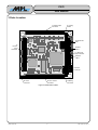
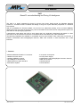
3 Parts Location
J1 Analog Input
Connector
S1 Config
Switch
BA
32
1
DCBA
CD
30
19
D4 Power OK
LED
8
7
6
5
4
J3
PC104+
(PCI)
Connector
3
2
1
O
N
D5 User
LED 0
J7 / J8 PC104
(ISA) Connector
D6 User
LED 1
0
1
1
J5 Power
Connector
1
1
1
J2 JTAG
Connector
J4 TPU / Serial
Connector
1
J6 Debug
Connector
Figure 3.1: PATI Parts Location
2009 by MPL AG
10
MEH-10102-001 Rev. D
PATI
User Manual
High-Tech • Made in Switzerland
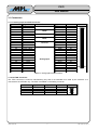
3.1 Connectors
3.1.1 J1 Analog Input and CAN Connector
Pin Number
1
3
5
7
9
11
13
15
17
19
21
23
25
27
29
31
33
35
37
39
41
43
45
47
49
Signal Name
rfu
rfu
GND
CAN2 Low
rfu
rfu
GND
CAN1 Low
rfu
rfu
rfu
GND
EXT_TRG1
CH8GND
CH7+
CH6GND
CH5+
CH4GND
CH3+
CH2GND
CH1+
I/O Function
reserved
CAN2
reserved
CAN1
reserved
Analog Input
Signal Name Pin Number
rfu
2
rfu
4
CAN2 High
6
GND
8
rfu
10
rfu
12
CAN1 High
14
GND
16
rfu
18
rfu
20
rfu
22
EXT_TRG2
24
GND
26
CH8+
28
CH730
GND
32
CH6+
34
CH536
GND
38
CH4+
40
CH342
GND
44
CH2+
46
CH148
GND
50
Pinout
1
2
49
50
Tabelle 3.1: Analog Input and CAN connector
3.1.2 J2 JTAG Connector
The JTAG connector is used for manufacturing only and is not intended to be used by the customer. It is
connected to the 2 EPLDs only. The CPU is available on the Debug connector
Pin Number
1
2
3
4
Signal Name
TDO
TDI
GND
GND
Signal Name Pin Number
TCK
8
TMS
7
VCC5
6
PORST#
5
Pinout
1
2
3
4
8
7
6
5
Tabelle 3.2: JTAG connector
2009 by MPL AG
11
MEH-10102-001 Rev. D
PATI
User Manual
High-Tech • Made in Switzerland
3.1.3 J3 - PC104+ Interface pin numbers
Number
1
2
3
4
5
6
7
8
9
10
11
12
13
14
15
16
17
18
19
20
21
22
23
24
25
26
27
28
29
30
Row A
GND
+5V
AD5
C/BE0
GND
AD11
AD14
(+3.3V)2
SERR
GND
STOP
(+3.3V) 2
FRAME
GND
AD18
AD21
(+3.3V) 2
IDSEL0
AD24
GND
AD29
+5V
REQ0
GND
GNT1
+5V
CLK2
GND
(+12V) 1
(-12V) 1
Row B
NC
AD2
GND
AD7
AD9
+5V
AD13
C/BE1
GND
PERR
(+3.3V) 2
TRDY
GND
AD16
(+3.3V) 2
AD20
AD23
GND
C/BE3
AD26
+5V
AD30
GND
REQ2
+5V
CLK0
+5V
INTD
INTA
NC
Row C
+5V
AD1
AD4
GND
AD8
AD10
GND
AD15
(SBO) 1
(+3.3V) 2
(LOCK) 1
GND
IRDY
(+3.3V) 2
AD17
GND
AD22
IDSEL1
+5V
AD25
AD28
GND
REQ1
+5V
GNT2
GND
CLK3
+5V
INTB
NC
Row D
AD0
+5V
AD3
AD6
GND
(M66EN) 1
AD12
(+3.3V) 2
PAR
(SDONE) 1
GND
DEVSEL
(+3.3V) 2
C/BE2
GND
AD19
(+3.3V) 2
IDSEL2
IDSEL3
GND
AD27
AD31
+5V
GNT0
GND
CLK1
GND
RST
INTC
GND
Pinout
ABCD
1
30
Tabelle 3.3: J10 PC/104 Plus connector
Notes:
1
2
2009 by MPL AG
Signal not available. (SBO, SDONE and LOCK are pull-up to 5V, M66EN is connected to GND and
+12V and -12V are not connected).
3.3V pins are connected to a plane, but not connected to the 3.3V Power Supply.
12
MEH-10102-001 Rev. D
PATI
User Manual
High-Tech • Made in Switzerland
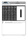
3.1.4 J4 TPU and Serial Connector
Pin Number
1
3
5
7
9
11
13
15
17
19
21
23
25
27
29
31
33
35
37
39
41
43
45
47
49
Signal Name
CH1
CH3
CH5
CH7
CH9
CH11
CH13
CH15
GND
CH17
CH19
CH21
CH23
CH25
CH27
CH29
CH31
GND
TPU_T2CLKA
GND
SPI_SDI
SPI_CS0#
GND
TXD1
TXD2
I/O Function
TPU
SPI
1st & 2nd RS232
Signal Name
CH2
CH4
CH6
CH8
CH10
CH12
CH14
CH16
GND
CH18
CH20
CH22
CH24
CH26
CH28
CH30
CH32
GND
TPU_T2CLKB
SPI_SDO
SPI_CLK
VCC5
RXD1
RXD2
GND
Pin Number
Pinout
2
1
2
4
6
8
10
12
14
16
18
20
22
24
26
28
30
32
34
36
38
40
42
44
49
50
46
48
50
Tabelle 3.4: TPU and Serial connector
3.1.5 J5 - Power Connector
This connector is needed for stand alone operation only.
3-pin power connector Phoenix Contact AG type MC1,5/3-G-3.81. Counterpart is the Phoenix Contact AG
connector type MC1,5/3-ST-3.81 (5-10A).
Pin number
1
2
3
Signal
VIN
GND
SRESET#
Description
Input voltage (+5 VDC)
Ground
System Reset Input (active low)
Pinout
1 2 3
Tabelle 3.5: J9 Power connector
2009 by MPL AG
13
MEH-10102-001 Rev. D
PATI
User Manual
High-Tech • Made in Switzerland
3.1.6 J6 - Debug Connector
The Debug Signals of the MPC555 is available on a 10Pin 2mm Header.
Pin Number
Signal Name
Signal Name Pin Number
1
VFLS0
SRESET#
2
3
GND
DSCK
4
5
GND
VFLS1
6
7
HRESET#
DSDI
8
9
VCC3
DSDO
10
Pinout
1
2
9
10
Tabelle 3.6: J6 Debug connector
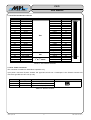
3.1.7 J7/8 - PC104 interface pin numbers
The PC104 (ISA) connector is not used on the PATI, only the power supply (+5V and GND Pins) are connected.
Number Row A
Row B
Row C
Row D
Pinout
0
--GND
GND
1
/IOCHCK
GND
/SBHE
/MEMCS16
2
SD7
RSTDRV
LA23
/IOCS16
3
SD6
+5V
LA22
IRQ10
4
SD5
IRQ9
LA21
IRQ11
5
SD4
(-5V)
LA20
IRQ12
AB
6
SD3
DRQ2
LA19
IRQ15
1
7
SD2
(-12V)
LA18
IRQ14
8
SD1
/ENDXFR
LA17
/DACK0
9
SD0
(+12V)
/MEMR
DRQ0
10
IOCHRDY
NC
/MEMW
/DACK5
11
AEN
/SMEMW
SD8
DRQ5
DC
12
SA19
/SMEMR
SD9
/DACK6
0
13
SA18
/IOW
SD10
DRQ6
14
SA17
/IOR
SD11
/DACK7
15
SA16
/DACK3
SD12
DRQ7
16
SA15
DRQ3
SD13
+5V
17
SA14
/DACK1
SD14
(/MASTER)
18
SA13
DRQ1
SD15
GND
19
SA12
/REFRESH NC
GND
20
SA11
SYSCLK
--21
SA10
IRQ7
--22
SA9
IRQ6
--23
SA8
IRQ5
--24
SA7
IRQ4
--19
25
SA6
IRQ3
--26
SA5
/DACK2
--27
SA4
TC
--28
SA3
BALE
--32
29
SA2
+5V
--30
SA1
OSC
--31
SA0
GND
--32
GND
GND
--Tabelle 3.7: PC/104 connector
2009 by MPL AG
14
MEH-10102-001 Rev. D
PATI
User Manual
High-Tech • Made in Switzerland
3.2 Switch
Default switch settings are bold.
3.2.1 DIP switch S1 –Configuration switch
Switch
S1-1
S1-2
S1-3
S1-4
S1-5
S1-6
S1-7
S1-8
On
Off
S1
PCI Slot Selection see below
PCI Disabled
Enable Boot
IP = 0 after reset
Boot from internal Flash
Use internal config word
not yet defined
Normal Operation
Disable Boot
IP = 1 after reset
Boot from external Flash
Use config word from PLD
not yet defined
1
2
3
4
5
6
7
8
O
N
Tabelle 3.8: S1: Software Configuration Switch
S1-1& S1-2: sets the PC104+ Slots. The Slot 1 is if the PATI is mounted direct on the host. Slot 2 is if there is
another card between the PATI and the host.
S1-2
S1-1 PCI Mux
Off
Off
Slot 1
Off
On
Slot 2
On
Off
Slot 3
On
On
Slot 4
S1-3:
PCI Disabled. If this switch is on, the PATI act in stand alone mode.
Do not switch on if using the PATI in PCI Agent mode! It will assert the PCI Reset Signal and
your host system will become inoperable!
S1-4:
If switched on, the PATI will boot regardless if it is initiated by the PCI host. If switched on the host
has to issue the Hardware configuration word to start-up the PATI.
S1-4..8:
These switches are not defined in the PCI Agent-mode. They are readable via the Software. In
Stand-alone Mode, these switches decide over different boot modes.
2009 by MPL AG
15
MEH-10102-001 Rev. D
PATI
User Manual
High-Tech • Made in Switzerland
4 Operation
The following chapters describes the operation of the PATI in the PCI Agent mode. The information are based
on the environment used for the first power-up and may not be valid for other environments.
4.1 Block Schematic
IO
Connector1
50Pin Dual
Row 2.54mm
TPU &
RS232
8Ch Analog In
Analog Filter
Analog Filter
32Channel TPU
RS232
Interface
RS232
Interface
RS232
Interface
RS232
Interface
Serial 0
PowerPC
PowerPC
MPC555
MPC555
Serial 1
CAN 1
Up to
Up to
16MByte
16MByte
SDRAM
SDRAM
soldered
on soldered
Board
on Board
System
System
Conroller
Conroller
PC/104+
Connector
PCI Part
PCI Bus
CAN 0
PCI Bridge
PCI Bridge
PLX9096
PLX9096
IO
Connector2
50Pin Dual
Row 2.54mm
Analog &
CAN
Local Bus
SDRAM
SDRAM
Conroller
Conroller
Power /Reset
Connector
Power
Power
Supply
Supply
Module
Module
Up to 8MByte
Up
to 8MByte
Flash
Flash
Figure 4.1: PATI Block Schematic
2009 by MPL AG
16
MEH-10102-001 Rev. D
PATI
User Manual
High-Tech • Made in Switzerland
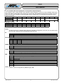
4.2 Mapping Overview
PCI Bridge
MPC555
EPLD
0x04001000.. 0x040010FF
0x07000000.. 0x070000FF
Direct Slave
Space 0
CS3
Local
Configurations
Register
0x04000000.. 0x04000FFF
CS2
IMMR Mapped
internal
peripherals
CPU: 0x03000000.. 0x03FFFFFF
Access only possible if
CPU in Slave Mode and
IMMR below 16MByte
PCI:0x01000000.. 0x01FFFFFF
Direct Master
Address
translation
CPU: 0x00000000.. 0x00FFFFFF
PCI:0x01000000.. 0x01FFFFFF
CS1
0x00000000.. 0x00FFFFFF
SDRAM
0x06000000.. 0x06FFFFFF
CS0
0xFFC00000.. 0xFFFFFFFF
Flash
0x03000000.. 0x03FFFFFF
Direct Slave
Space 1
Figure 4.2: PATI Mapping Overview
Note:
●
Accessing the CPU is only possible if taking the MPC555 in slave mode and change the IMMR
Address below the first 16MByte.
2009 by MPL AG
17
MEH-10102-001 Rev. D
PATI
User Manual
High-Tech • Made in Switzerland
4.3 Used Environment
To have full access to the PCI resources the environment used to test the PATI consist of a PCI Host (MIP405)
without a operating system. Instead a special version of the bootloader „U-Boot“ has been used.
The bootloader on the PATI is also a special version of the „U-Boot“
4.4 Local Memory Map
Although the PATI supports different boot modes, only the boot from external flash is used so far, and therefore
discussed in this document.
The „U-Boot“ requires to have the SDRAM started from address 0, but with other software other mapping is
also possible.
Local Address
CS
Area
Size
Bus Size
0x00000000-0x00FFFFFF
CS1
SDRAM
16MByte 32Bit
0x01C00000-0x01FFFFFF
none
MPC Internal Registers and Memory
4MByte
32Bit
0x03000000-0x03FFFFFF
CS2
PCI Master Area (Mapped to PCI)
16MByte 32Bit
0x04000000-0x04000FFF
CS3
PCI Bridge Configuration Area
4KByte
32Bit
0x04001000-0x0400101F
CS3
EPLD Config Address
32Byte
32Bit-only
0xFFC00000-0xFFFFFFFF
CS0
External Flash
4MByte
16Bit-only
Tabelle 4.1: Local Memory Map
Notes:
• The EPLD Config Area and the External Flash are accessible only in their bus size. The byte enable
signals on these areas are ignored.
• Access to all areas are self-timed, which means, the MPC555 memory controller has to be programmed
with the SETA bit.
• Since the IP Bit is set on start-up the MPC555 fetches its first instruction from the flash at address
0xFFF00100.
• The PCI Master area is seen on the address 0x01000000 on the local bus of the PCI Bridge, not on
address 0x03000000. This is because the CS2 issues 0x01XXXXXX to the PCI Bridge
This mapping leads to the following MPC555 memory controller definition:
/* CS0 (Flash): Bank Valid, Burst Inhibit, Port Size 16Bit External TA */
#define BR0
0xFFC00807
#define OR0
0xFFC00000 /* SCY is not used if external TA is set */
/* CS1 (SDRAM): Bank Valid, Burst Inhibit, Port Size 32Bit, External TA */
#define BR1
0x00000007
#define OR1
0xFF000000 /* SCY is not used if external TA is set */
/* CS2 (PCI): Bank Valid, Burst Inhibit, Port Size 32Bit, External TA */
#define BR2
0x03000007
#define OR2
0xFF000000 /* SCY is not used if external TA is set */
/* CS3 (Config registers): Bank Valid, Burst Inhibit, Port Size 32Bit, External TA */
#define BR3
0x04000007
#define OR3
0xFFFF0000 /* SCY is not used if external TA is set */
The internal Memory mapping is mapped via the Hardware Configuration word to 0x01C00000, set the Bits
ISB[0..3] to 0x7.
#define IMMR 0x01C00000 /* Physical start address of internal memory map */
The „U-Boot“ bootloader fetches the first instruction from 0xFFF00100 and reprograms the IP bit to 0 during
initialization, in order to set-up its exceptions in the SDRAM. So set the IP bit to 1 in the hardware configuration
word.
2009 by MPL AG
18
MEH-10102-001 Rev. D
PATI
User Manual
High-Tech • Made in Switzerland
4.5 PCI Memory Map
4.5.1 PCI Bridge Local Bus Memory Mapping
Since the PCI Bridge don’t have a chipselect logic, the local mapping of the PCI bridge is fixed:
Local Area
Range
Descriptor
SDRAM
0x06000000-0x06FFFFFF
TA enable, no burst, prefetch, 32Bit port size
External Flash
0x03000000-0x03FFFFFF
TA enable, no burst, no prefetch, 16Bit port size
EPLD Registers
0x07000000-0x07FFFFFF
TA enable, no burst, no prefetch, 32Bit port size
CPU
0x01000000-0x01FFFFFF
TA enable, no burst, no prefetch, 32Bit port size
Tabelle 4.2: PCI Bridge Local Bus Memory Map
Notes:
• Areas smaller than 16MByte are mirrored over the entire 16MByte range.
• The CPU access is only possible if taking the MPC555 in slave mode and change the IMMR Address
below the first 16MByte.
4.5.2 PCI Bridge PCI Memory Map
The PCI addresses are full configurable on the PCI side. In a PC environment the configuration space must be
mapped to the IO Space, all others areas are mapped to the memory space.
The term „Direct Slave“ denotes an area whereas the PCI host can access local memory. The term „Direct
Master“ denotes an area whereas the MPC555 can access PCI host memory.
To save PCI resources the direct slave space 0 is assigned to the PLD configuration area and its size has been
restricted to 256bytes. The size of the direct slave space 1 is 1MByte and this space can be used for all other
areas, by reprogram the LAS1BA (base address) and LBRD1 (Bus descriptor) registers.
PCI Area
Base Register
Size
Default local Area
PCIBAR0
Configuration Space
512Bytes
PCI Bridge configurations Registers
@ PCI Config Cycle + 0x10
Configuration
PCIBAR1
256Bytes
PCI Bridge configurations Registers
Space I/O
@ PCI Config Cycle + 0x14
PCIBAR2
Direct Slave Space 0
256Bytes
EPLD configuration Registers
@ PCI Config Cycle + 0x18
PCIBAR3
Direct Slave Space 1
1MBytes
SDRAM (@ 0x00000000)
@PCI Config Cycle + 0x1C
DMPBAM
Direct Master Space
1MBytes
PCI Area (@ 0x03000000)
@PCIBAR0 + 0x28
Tabelle 4.3: PCI Bridge PCI Memory Map
The EEPROM on the PATI sets all local addresses, and sizes on start-up. The host BIOS should set the PCI
addresses where these areas are accessible from the PCI bus.
4.5.3 Direct Slave Space 0 Mapping
The Direct Slave Space 0 is mapped by the EEPROM to the EPLD area. This leads to following register
contents:
Register
Contents
Description
LAS0RR
0xFFFFFF00 Range Register (256B)
(PCIBAR0+0x00)
LAS0BA
0x07000001
Local address of the EPLD and enabled
(PCIBAR0+0x04)
LBRD0
Bus Descriptor: clear [24] (no burst), set [8] (no prefetch), set [6]
0x42430143
(PCIBAR0+0x18)
(TA enable), set [1..0] to 0x3 (bussize 32bit)
Tabelle 4.4: Direct Slave Space 0 Register for EPLD access
2009 by MPL AG
19
MEH-10102-001 Rev. D
PATI
User Manual
High-Tech • Made in Switzerland
4.5.4 Direct Slave Space 1 Mapping
The Direct Slave Space 1 can be used to access the SDRAM, Flash and CPU. It’s size is 1MByte. To access
an address which lies over the size of the Direct Slave Space 1, the higher part of the address has to be added
to the local base address and written to the LAS1BA register. For example, an access to the SDRAM address
0x0089ABCD takes place when the LAS1BA register is programmed to 0x06800001 and an access at
„pci_address_of_direct_space1“ (contents of PCIBAR3) + 0x0009ABCD is performed.
The SDRAM area is the default mapping of the Direct Slave Space 1. This leads to following register contents:
Register
Contents
Description
LAS1RR
0xFFF00000 Range Register (1MByte)
(PCIBAR0+0xF0)
LAS1BA
0x06000001
Local address of the SDRAM and enabled
(PCIBAR0+0xF4)
LBRD1
Bus Descriptor: clear [8] (no burst), clear [9] (prefetch), set [6]
0x00000043
(PCIBAR0+0xF8)
(TA enable), set bit[1..0] to 0x3 (bussize 32bit)
Tabelle 4.5: Direct Slave Space 1 Register for SDRAM access
To map the Direct Slave Space to other areas the registers „Direct Slave Space 1 Local Base Address
(Remap)“ and „Local Address Space Local 1 Bus Descriptor“ must be set accordingly. The range register
should not be touched because the PCI mapping done by the BIOS relies on the size of the initial configuration.
Following contents is used to access the flash:
Register
Contents
Description
LAS1BA (PCIBAR0+0xF4) 0x03000001
Local address of the Flash and enabled
Bus Descriptor: clear [8] (no burst), set [9] (no prefetch), set
LBRD1 (PCIBAR0+0xF8)
0x00000241
[6] (TA enable), set [1..0] to 0x1 (bussize 16bit)
Tabelle 4.6: Direct Slave Space 1 Register for Flash access
Following contents is used to access the CPU:
Register
Contents
Description
LAS1BA (PCIBAR0+0xF4) 0x01000001
Local address of the CPU and enabled
Bus Descriptor: clear [8] (no burst), set [9] (no prefetch), set
LBRD1 (PCIBAR0+0xF8)
0x00000243
[6] (TA enable), set [1..0] to 0x3 (bussize 32bit)
Tabelle 4.7: Direct Slave Space 1 Register for CPU access
Note:
●
The CPU access is only possible if taking the MPC555 in slave mode and change the IMMR Address
below the first 16MByte.
4.5.5 Direct Master Mapping
The CS2 signal is used to select the direct master area on the PCI Bridge. The EPLD converts the CS2 signal
to the local address 0x01XXXXXX. So the PCI Bridge sees the access to the direct master area on the local
address 0x01000000.
Register
Description
Access
DMRR
Local Range for Direct Master-to-PCI
PCIBAR0+0x1C
DMLBAM
Local Base Address for Direct Master-to-PCI Memory
PCIBAR0+0x20
DMPBAM
PCI Base Address (Remap) for Direct Master-to-PCI Memory
PCIBAR0+0x28
Tabelle 4.8: Register used to configure direct master access
Note:
●
The base address in the register DMPBAM will be set from the PCI host, when enabling the master
access.
2009 by MPL AG
20
MEH-10102-001 Rev. D
PATI
User Manual
High-Tech • Made in Switzerland
The default mapping of the direct master access leads to following register contents:
Register
Contents
Description
DMRR (PCIBAR0+0x1C)
0xFFF00000
Range Register (1MByte)
DMLBAM (PCIBAR0+0x20)
0x01000000
Local master address
DMPBAM (PCIBAR0+0x28) 0xXXXX0001
bit[31..16] PCI Address, bit[15..0] 0x0001, Enabled
Tabelle 4.9: Default register contents for master access
4.6 Hardware Configuration Word
To have this flexibility on the PAT, it is necessary to control the start-up behavior of the MPC555. Therefore
Parts of the Hardware configuration word for the MPC555 is writable via the PCI Bridge.
4.6.1 Writing the Hardware Configuration Word
This is done via the USERo Signal and the EEPROM channel:
1. Assert LRESET# => asserts Power-On Reset / System Reset
2. Deassert USERo USERo=0 = reset
3. Deassert LRESET# => PLL of CPU Starts but since the USERo is deasserted, HRESET# is asserted.
4. Write the configuration via the EEPROM Channel into the PLD. Data is latched with the rising edge of the
clock
5. Assert USERo => HRESET# is released and the Hardware Configuration Word is latched in.
Following code is used for this purpose:
/*******************************************************************
* set the EECLK High, wait some time, set EECLK low again
*******************************************************************/
void clock_eeprom(void)
{
unsigned long reg;
/* clock is low, data is valid */
reg = read32cfg (pci_cfg_mem_base + PCI9056_EEPROM_CTRL_STAT);
udelay(1);
/* set clock high */
reg |= (1<<24);
write32cfg (pci_cfg_mem_base + PCI9056_EEPROM_CTRL_STAT,reg);
/* wait some time */
udelay(1);
/* set clock low */
reg &= ~(1<<24);
write32cfg(pci_cfg_mem_base + PCI9056_EEPROM_CTRL_STAT,reg);
/* wait some time */
udelay(1);
}/*******************************************************************
* Write HW config word. Bit 11 in config is Bit 11 of Hardware config word
*******************************************************************/
void write_hw_config(unsigned long config)
{
/* we write the config via the BAR0 register into the configuration */
unsigned long reg;
int i;
reg=read32cfg(pci_cfg_mem_base + PCI9056_EEPROM_CTRL_STAT);
/* first assert LRESET */
reg |= 1<<19; /* assert reset set usero as usero */
write32cfg(pci_cfg_mem_base + PCI9056_EEPROM_CTRL_STAT,reg);
udelay(100); /* wait some time */
reg &= ~((1<<16)+(1<<24)); /* clear usero and clock */
write32cfg(pci_cfg_mem_base + PCI9056_EEPROM_CTRL_STAT,reg);
udelay(100); /* wait some time */
reg |= (1<<25); /* set EECS */
write32cfg(pci_cfg_mem_base + PCI9056_EEPROM_CTRL_STAT,reg);
udelay(100); /* wait some time */
/* write data bits (D11 first, D0 last) */
for(i=11;i>=0;i--) {
/* clock is low */
if((config & (1<<i))==0)
reg &= ~(1<<26); /* clear bit */
else
reg |= (1<<26); /* set bit */
write32cfg(pci_cfg_mem_base + PCI9056_EEPROM_CTRL_STAT,reg);
clock_eeprom();
2009 by MPL AG
21
MEH-10102-001 Rev. D
PATI
User Manual
High-Tech • Made in Switzerland
}
/* written, take it out from reset */
reg &= ~(0xF << 24); /* clear all EEPROM bits */
/* set usero */
udelay(100);
write32cfg(pci_cfg_mem_base + PCI9056_EEPROM_CTRL_STAT,reg | (1<<16));
/* clear usero */
write32cfg(pci_cfg_mem_base + PCI9056_EEPROM_CTRL_STAT,reg & ~(1<<16));
udelay(100);
/* set usero */
write32cfg(pci_cfg_mem_base + PCI9056_EEPROM_CTRL_STAT,reg | (1<<16));
udelay(100);
}
4.6.2 Hardware Configuration Word description
The first programmed date is D11, the last is D0.
Bit
D11
D10
D9
D8
D7
D6
Desc PCIM
BDIS PRPM CONF ISB0
ISB1
D5
ISB2
D4
IP
D3
FLAG
D2
D1
D0
Boot Index
Tabelle 4.10: Hardware configuration Bits
PCIM:
PCIM
0
1
Desc
Normal Operation (CPU and PCI Bridge can access the local bus)
PCI Only Mode (Only PCI Bridge can access the local bus)
BDIS:
BDIS
0
1
Desc
Memory bank 0 is active and matches all addresses immediately after reset (default)
Memory controller is not activated after reset
PRPM
0
1
Desc
RCPU starts up normal (default)
RCPU starts up in Slave Mode
CONF
0
1
Desc
Hardreset Config is sampled from PLD (default if SW1-7 = Off)
Hardreset Config is sampled from internal Flash (default if SW1-7 = On)
PRPM:
CONF:
ISB:
ISB[2..0]
000
001
010
011
100
101
110
111
Base address of the internal memory space.
0x0000 0000
0x0040 0000
0x0080 0000
0x00C0 0000
0x0100 0000
0x0140 0000
0x0180 0000
0x01C0 0000 (default)
IP:
IP
0
1
Desc
Exception vector table starts at 0x0000 0000 (default if SW1-5 = On)
Exception vector table starts at 0xFFF0 0000 (default if SW1-5 = Off)
FLAG:
This Bit can be set or cleared when writing the Hardware configuration word and can be read back by
the local CPU. May be used for deciding the start-up mode
Boot Index:
D2
D1
D0
0
0
0
Boot from External Flash (default if SW1-4 = Off)
0
0
1
Boot from Internal Flash (default if SW1-4 = On)
0
1
1
Boot from PCI
1
0
1
Boot from SDRAM
2009 by MPL AG
22
MEH-10102-001 Rev. D
PATI
User Manual
High-Tech • Made in Switzerland
4.7 EPLD Configuration Register
4.7.1 Configuration Registers Mapping
Area
Size
PCIBridge Registers 4KByte
PLD Registers
4KByte
CPU
CS3# +0x00000000 .. 0x00000FFF
CS3# +0x00001000 .. 0x00001FFF
PCI
Access via base address in PCIBAR0
0x07000000 .. 0x07001FFF
Tabelle 4.11: EPLD Configuration Register Mapping
4.7.2 EPLD Registers
The EPLD Register are located in a 32Bit wide area but not all bits are useable. Since 2 EPLDs are using the
same config area, the registers are fragmented:
Bits
D0
D1
D2
D3
D4
D5
D6
D7
D8
D9 D10 D11 D12 D13 D14 D15
SYS
X
X
X
X
X
SDRAM
X
X
X
X
X
X
Bits
D16
SYS
X
SDRAM
D17
D18
D19
D20
X
D21
D22
D23
D24
D25
D26
D27
X
D28
X
D29
X
D30
X
D31
X
Tabelle 4.12: EPLD Configuration Register Bits
Whereas SYS denotes the Source from the System Controller, and SDRAM the SDRAM Controller.
Notes:
• Access to the EPLD register must be done as 32bit access only, the byte enable lines are ignored in this
area.
• To reset these register a Power-On or LRESET (from the PCI Bridge) is used. So it is possible for the local
CPU to write a new Hardware config word and performs a HRESET to start-up in the new configuration.
4.7.3 PLD Register Map
Address Offset
0x00
0x04
0x08
0x0C
0x10
Description
PLD ID Register
Board Revision, Timing and SDRAM Controller Register
Hardware Word Config Register and Population Option Register
Misc Config Register
Reset Register (a write to this Register asserts the HRESET#)
Tabelle 4.13: EPLD Configuration Register Address
4.7.3.1 EPLD ID Register
The EPLD ID Register is used to identify the EPLD Part and Version. Depending on these ID’s the Registers
may differ. This Document describes the initial Version (V00, P00 and V00, P01) of the EPLD’s.
System Controller
Bits
D0
D1
D3
D4
D5
D16
D20
D28
D29
D30
Read
Part ID
Version
Default
0
0
SDRAM Controller:
Bits
D9
D10
D11
D12
D13
D14
D19
D31
Read
Part ID
Version
Default
1
0
Tabelle 4.14: EPLD Part ID Register
2009 by MPL AG
23
MEH-10102-001 Rev. D
PATI
User Manual
High-Tech • Made in Switzerland
4.7.3.2 Board Revision & Timing / SDRAM Controller Register
System Controller
Bits
D0
D1
D3
D4
D5
D16
Read
Board Revision
Res
Res
Write
0
0
0
Default
0
X
X
SDRAM Controller:
Bits
D9
D10
D11
D12
D13
D14
Read
CAL
RCD
WREQ
PR
RC
LMR
Write
Default
0
0
0
0
0
0
D20
Res
0
X
D19
IIP
0
D28
D29
D30
Wait0
Wait1
Wait2
1
1
1
D31
0
Res
0
Tabelle 4.15: Board Revision & Timing Register
Board Revision:
Binary value of the PCB Revision (D0 is MSB) currently 0000.
Waitx:
Waitstates for Flash access: Access = waitx + 3 clocks. Default 7
CAL:
CAL
Desc
0
CAS Latency 2
1
CAS Latency 3
RCD:
RCD
Desc
0
ACTIVE to READ or WRITE Delay (RAS to CAS Delay) <= 25ns
1
ACTIVE to READ or WRITE Delay (RAS to CAS Delay) <= 50ns
WREQ:
WREQ Desc
0
Write Recovery tWR <= 25ns
1
Write Recovery tWR <= 50ns
PR:
PR
Desc
0
Precharge Command Time tPR <= 25ns
1
Precharge Command Time tPR <= 50ns
RC:
RC
Desc
0
Auto Refresh to Active Time <= 75ns
1
Auto Refresh to Active Time <= 100ns
LMR:
Set this bit to write the Mode Register of the SDRAM. If set, the next access to the SDRAM is the Load
Mode Register Command.
IIP:
Set this bit to initialize the SDRAM. Setting this bit issues a PRECHARGE_ALL command to the
SDRAM, if read back as 0, the PRECHARGE_ALL command has been issued.
To set-up the SDRAM follow these steps:
• If set-up via the PCI Bridge, set the direct slave space 1 to the SDRAM start.
• Set the bits CAL, RCD, WREQ, PR and RC in the Register.
• Set the bit IIP to issue a PRECHARGE_ALL command.
• After the IIP is read back 0 wait at least for 9 refresh cycles (ca. 200usec)
• calculate the contents of the mode register, set the LMR bit and read from the address
MODE_REGISTER + SDRAM_START.
CAS Latency
MODE_REGISTER Description
CAL = 2
0x00000088
Sequential burst 4 data, CAL 2 => 0x00000022 << 2
CAL = 3
0x000000C8
Sequential burst 4 data, CAL 3 => 0x00000032 << 2
2009 by MPL AG
24
MEH-10102-001 Rev. D
PATI
User Manual
High-Tech • Made in Switzerland
4.7.3.3 Hardware Word Config Register and Population Option Register
The Hardware Word Config Register and Population Option Register is used to set the Hardware Reset word.
Since this doesn’t make sense if the CPU is up and running, this Register should only be read by the CPU.
Some of these bits are settable via the EEPROM channel, please refer to 4.6 Hardware Configuration Word.
System Controller
Bits
D0
D1
D3
D4
D5
D16
D20
D28
D29
D30
Read
FLAG
IP
Boot Config Index
PRPM CONF
ISB
Write
Default
0
0
0
0
0
0
0
0
0
0
SDRAM Controller:
Bits
D9
D10
D11
D12
D13
D14
D19
D31
Read
CFG0
CFG1
CFG2
CFG3
CFG4
CFG5
CFG6
Res
Default
0
0
0
0
0
0
0
0
Tabelle 4.16: Hardware Word Config Register and Population Option Register
FLAG:
This Bit can be set or cleared when writing the Hardware configuration word and can be read back by
the local CPU. May be used for deciding the start-up mode
IP:
IP
Desc
0
After reset Exception vector table starts at the physical address 0x0000 0000 (default)
1
After reset Exception vector table starts at the physical address 0xFFF0 0000
Boot Index:
D3
D4
D5
0
0
0
Boot from External Flash (default)
0
0
1
Boot from Internal Flash
0
1
1
Boot from PCI
1
0
1
Boot from SDRAM
PRPM:
PRPM Desc
0
RCPU starts up normal (default)
1
RCPU starts up in Slave Mode
CONF:
CONF Desc
0
Hardreset Config is sampled from PLD (default)
1
Hardreset Config is sampled from internal Flash
ISB:
ISB
Base address of the internal memory space.
000
0x0000 0000 (default)
001
0x0040 0000
010
0x0080 0000
011
0x00C0 0000
100
0x0100 0000
101
0x0140 0000
110
0x0180 0000
111
0x01C0 0000
CFGx:
Used for various Configurations (SDRAM Type) TBD.
2009 by MPL AG
25
MEH-10102-001 Rev. D
PATI
User Manual
High-Tech • Made in Switzerland
4.7.3.4 Misc Config Register
The Misc Config Register is used to set the Hardware Reset word. Since this doesn’t make sense if the CPU is
up and running, this Register should only be read by the CPU. Some of these bits are settable via the
EEPROM channel, please refer to 4.6 Hardware Configuration Word.
System Controller:
Bits
D0
D1
D3
D4
D5
D16
D20
D28
D29
D30
Read
Config Inputs
BEN
CPU
EXT
EXT
BDIS
PCIM
VPP
VPP
WP
Write
Default
0
0
X
X
X
X
X
0
0
0
SDRAM Controller:
Bits
D9
D10
D11
D12
D13
D14
D19
D31
MUX0
MUX1
Res
Res
Res
Res
Res
Res
Default
X
X
0
0
0
0
0
0
Tabelle 4.17: Misc Config Register
BDIS:
BDIS
0
1
Desc
Memory bank 0 is active and matches all addresses immediately after reset (default)
Memory controller is not activated after reset
PCIM:
PCIM Desc
0
Normal Operation (default)
1
PCI is the only Master on the Local Bus. Bus Request from CPU is ignored.
Config Inputs:
These Bits are set if the corresponding DIP switch is on. CFG0 is D3 and CFG4 is D20.
Normal Mode:
S4..S8
Description
Off
CFGx = 0
On
CFGx = 1.
Standalone Mode:
S4
CFG0 Description
Off
0
IP = 0
On
1
IP = 1.
S5
CFG1 Description
Off
0
Boot from external Flash
On
1
Boot from internal Flash
S6
CFG2 Description
Off
0
Hardreset Config is sampled from PLD (default)
On
1
Hardreset Config is sampled from internal Flash
BEN:
BEN
Desc
0
Boot disabled (no auto startup on power on) SW1-4 is Off
1
Boot enabled SW1-4 is On.
CPU_VPP:
CPU_VPP
Description
0
VPP for the internal Flash is switched off (default)
1
VPP for the internal Flash is switched on
EXT_VPP:
EXT_VPP Description
0
VPP for the external Flash is switched off (default)
1
VPP for the external Flash is switched on
EXT_WP:
CPU_VPP Description
0
External Flash is not write protected (default)
1
External Flash is write protected
2009 by MPL AG
26
MEH-10102-001 Rev. D
PATI
User Manual
High-Tech • Made in Switzerland
MUX[0..1]:
Signals from PCI Muxers:
Switch
Bits
S5
S6
MUX1
MUX0
Off
Off
0
0
Off
On
0
1
On
Off
1
0
On
On
1
1
PCICLK
PCIIRQ#
REQ#/GNT#
Description
CLK0
CLK1
CLK2
CLK3
IRQA#
IRQB#
IRQC#
IRQD#
REQ0#/GNT0#
REQ1#/GNT1#
REQ2#/GNT2#
REQ2#/GNT2#
Slot 0
Slot 1
Slot 2
Slot 3
4.7.3.5 Reset Register
A write to the Reset Register (offset = 0x010) causes the assertion of the HRESET#.
4.8 Resets
The various reset sources of the PATI are assigned to following 3 reset states:
CPU
Reset States
PORST#
HRESET#
SRESET#
Power-On Reset
asserted
asserted
asserted
HRESET#
deasserted
asserted
asserted
SRESET#
deasserted
deasserted
asserted
EPLD
Registers
reset
not reset
not reset
Table .4.18 Reset States
Reset source
PCI RST#
PCI Software Reset (CNTRL[30]=1) (asserts
LRESET#)
PCI
Bridge
USERO
=
0
(CNTRL[19]=1,
CNTRL[16]=0)
Local Power-On Reset
CPU HRESET#
CPU SRESET#
EPLD write to the Reset Register (offset = 0x010)
Reset State
Power-On Reset
Power-On Reset
Remarks
Resets also the entire PCI Bridge
Resets parts of the PCI Bridge
HRESET#
State to write the HW Config
Word
Power-On Reset
HRESET#
SRESET#
HRESET#
Table .4.19 Reset Sources
4.9 Interrupts and I/Os
Several different states of the PCI Bridge may cause the assertion of the LINTo of the PCI Bridge. This allows
the host to interrupt the local CPU.
The local CPU may interrupt the host by setting certain register bits in the PCI Bridge, which causes the
assertion of the PCI INT# signal. Additional the LINTi# signal of the PCI Bridge is connected to the CPU, with
which the local CPU may also issue a PCI interrupt.
Two CPU I/O signals are connected to user LED’s, with which the local CPU can signal different states to the
user.
Following table shows the assigning of the interrupt and I/O Signals:
CPU
Connected to
Signal
Configured Direction Device
Remarks
IRQ1#/RSV#/GPIO1
IRQ1#
Input
PCI Bridge INTO#
Host interrupts local CPU
GPIO7/IRQOUT#/LWP0
GPIO7
Output
PCI Bridge INTI#
Local CPU interrupts Host
IRQ2#/CR#/GPIO2/MTS#
GPIO2
Output
PCI Bridge USERi# Not yet used
IRQ5#/GPIO5/MODCK1
GPIO5
Output
User LED0
If set LED is on
GPIO6/FRZ/PTR#
GPIO6
Output
User LED1
If set LED is on
Table .4.20 Interrupts and I/O routing
2009 by MPL AG
27
MEH-10102-001 Rev. D
PATI
User Manual
High-Tech • Made in Switzerland
5 Operation via the PCI bus
5.1 Normal Set-Up
This chapter describes how to set-up the PCI Bridge if the EEPROM is programmed.
1. Find the PCI Device with the Vendor ID 0x18E6 Device ID 0x00DA.
2. The bits Memory Space access, IO Space access and Master enable in the PCI Command register should
be already set by the BIOS
3. Get the four Base Address for:
•
PCI Bridge config access in I/O space (PCIBAR1)
•
PCI Bridge config access in Memory space (PCIBAR0)
•
Direct Slave Space 0 (EPLD Config Registers) (PCIBAR2)
•
Direct Slave Space 1 (SDRAM Access) (PCIBAR3)
4. Depending on your host system you may set the endian register (BIGEND @ PCIBAR0 + 0x0C)
5. If the PATI is not in the Boot direct mode, clear USERO and set it again, to start the PATI up.
6. You could now reprogram the direct slave space 1 Registers to access another area than the SDRAM.
7. If using the direct master mode, program the Direct Master Registers accordingly.
5.2 Set-Up without programmed EEPROM
Setting up the PCI Bridge without programmed EEPROM is only needed, if the EEPROM has been erased or
wrongly programmed before.
Note:
Be careful if you assign PCI addresses to the different PATI address spaces. The host BIOS
may have already assigned the PCI address you like to assign. It is recommended, only to
reprogram the EEPROM in this state and reboot the system.
1.
2.
3.
4.
5.
6.
7.
6.
Find the PCI Device with the Vendor ID 0x10B5 Device ID 0x9056. (default PLX IDs)
Set the bits Memory Space access and IO Space access in the PCI Command register
Get the Config Base Address by reading the PCIBAR0.
Set registers LAS0RR, LAS0BA, LBRD0 and LAS1RR, LAS1BA, LBRD1 to a valid value.
Write 0xFFFFFFF0 to the registers PCIBAR2 and PCIBAR3.
Read the registers PCIBAR2 and PCIBAR3 back to determinate the size value.
Set the registers PCIBAR2 and PCIBAR3 to a valid value.
Read the register PCIBAR2 and PCIBAR3 to get the base address of the direct slave space0 and space1
area.
5.3 Set-Up the PATI via PCI Bridge
After the PCI Bridge is set up, you may want to program the flash or set-up the SDRAM without the local CPU
intervention. This can be done by writing the Hardware Configuration word accordingly.
To disable the CPU set the bit PCIM and the PRPM bit in the hardware configuration word. You may set also
the ISP bits to an address below 16MByte to have access to the CPU peripheries. After the Hardware
configuration word is written you have access via the PCI Bridge to the area you have programmed in the
LAS0RR, LAS0BA, LBRD0 and the LAS1R, LAS1A, LBRD1 Registers.
5.4 Program the Flash
To erase/program the external flash, you have to configure to have access to the EPLD configuration Registers
and to the Flash area.
1. Set the external Flash VPP, by setting the Bit EXT_VPP and clearing the Bit EXT_WP in the Misc Config
Register. Note: Access to the EPLD area MUST be done 32 bit wide. So read the register first, set/clear
the bits and write it back.
2. Determinate the flash type by reading its ID, and erase/program it according the specified algorithm. Refer
to the datasheet of the respective flash manufacturer for details. Note: Access to the Flash MUST be
done in 16Bit mode only. Please calculate the flash address via the various mapping register to get the
physical starting address from the PATI.
2009 by MPL AG
28
MEH-10102-001 Rev. D
PATI
User Manual
High-Tech • Made in Switzerland
5.5 Set-Up the SDRAM
In normal operation, the SDRAM is set-up by the firmware on the PATI itself. So set-up the SDRAM from the
PCI Bridge is only necessary in special cases, such as booting directly from SDRAM. To set-up the SDRAM,
you have to configure to have access to the EPLD configuration Registers and to the SDRAM area.
1. Set the bits CAL, RCD, WREQ, PR and RC in the Board Revision & Timing / SDRAM Controller Register
according to the populated SDRAM Chips. (currently: CAL=1, RCD=0, WREQ=0, PR=0, RC=0).
Note:
Access to the EPLD area MUST be done 32 bit wide. So read the register first, set/clear the bits
and write it back.
2. Set the bit IIP in the Board Revision & Timing / SDRAM Controller Register. This issues a precharge all
command to the SDRAM.
3. Poll the IIP Bit and if it is cleared wait for at least 8 refresh (200usec) before proceeding (8 refresh a 17usec
= 136usec).
4. Set the bit LMR in the Board Revision & Timing / SDRAM Controller Register. This causes the next access
is a set mode register command to the SDRAM.
5. The Mode register address is 0x0C8 if the CAL bit is 1 and 0x88 if CAL is 0.
6. Read from the SDRAM Start + Mode Register Address, to load the value into the SDRAM.
The SDRAM should now be accessible normal.
5.6 Start-Up the PATI
To start-up the local CPU write the hardware configuration word with the PCIM and the PRPM cleared. The
default hardware configuration word is 0x00F0. If using in the default configuration, it is sufficient to clear the
USERo bit and set it again.
If the S1-4 is On, the PATI starts with the default configuration word after power-up.
2009 by MPL AG
29
MEH-10102-001 Rev. D
PATI
User Manual
High-Tech • Made in Switzerland
6 Open issues
6.1 Flash access problem while programming the MPC555 PLL
When programming the MPC555 PLL to 40MHz, the access to the external flash fails. The reason is that the
CLOCK Out Signal of the MPC555 is unstable in this state. To solve this problem the part which programs the
PLL is copied into the internal SRAM and executed from there.
6.2 MPC555 does not allows access to the internal Peripheries.
The MPC555 does not allow access to it’s internal peripheries while running in normal mode. In Slave Mode
(Bit PRPM set), this access works. This problem has not yet been solved, since the U-Boot mapping doesn’t
allow the access to the internal peripheries anyway. This is because the internal peripheral must be mapped
below the first 16MByte to allow external master access, and this entire area is assigned to the SDRAM.
6.3 MPC555 asserts resets if using PATI in PCI only mode or slave mode.
Since the MPC555 watchdog is enabled after a power-on reset, the MPC555 asserts HRESET if the CPU does
not get the local bus (PCI-only mode) or/and it is configured in slave mode. This may lead to erroneous access
which may even cause a system hang.
Workaround:
• configure the PATI in PCI only mode, CPU slave and IMMR below 16MBytes
• disable the watchdog (write 0xFFFFFF01 to the SYPCR Register
6.4 PLX Bridge hangs if an access doesn’t terminate (missing TA).
If a direct slave access is disturbed by a HRESET (happens only, if the MPC555 is not running), the PLX
Bridge waits forever for a TA. To reset the PLX Bridge a Power-on reset is needed.
Workaround:
• Program the PLX Register “(LMISC2; PCI:0Fh, LOC:8Fh) Local Miscellaneous Control 2“ to 0x0330. This
causes a PCI Target Abort if the TA is not sampled within 1024 local bus clocks after TS. Please note, that
on the PLX Bridge no method exists to detect this failure. The register should only be modified, on debug
purposes.
2009 by MPL AG
30
MEH-10102-001 Rev. D
PATI
User Manual
High-Tech • Made in Switzerland
7 Debug Cable wiring
To connect the PATI to an ABATRON BDI2000 (or similar Debuging Tools) an atapter cable is necessary.
Please use the following wiring:
PATI J6
BDI2000 TARGET A
10pin 2mm Header
10pin 2.54mm Header
female.
female
Pin Number
Signal
Pin Number
1
VFLS0
1
2
SRESET#
2
3
GND
3
4
DSCK
4
5
GND
5
6
VFLS1
6
7
HRESET#
7
8
DSDI
8
9
VCC3
9
10
DSDO
10
Tabelle 7.1: Debug Cable wiring
Notes:
• Please consult the documentation of your debug tool details.
2009 by MPL AG
31
MEH-10102-001 Rev. D
PATI
User Manual
High-Tech • Made in Switzerland
8 COPYRIGHT
Copyright © 2009 by MPL AG Elektronikunternehmen. All rights are reserved. Reproduction of this document in
part or whole, by any means is prohibited, without written permission from MPL AG Elektronikunternehmen.
9 DISCLAIMER
MPL AG has fully tested the PATI and reviewed the documentation. However, MPL AG makes no warranty or
representation, either expressed, or implied, with respect to this product, its quality, performance,
merchantability, or fitness for a particular purpose.
In no event will MPL AG be liable for direct, indirect, special, incidental, or consequential damages resulting
from any defect in the product or its documentation, even if advised of the possibility of such damages. In
particular MPL AG shall have no liability for any parts connected to this product.
MPL AG reserves the right to make changes to any product herein to improve reliability, function or design.
10 TRADEMARKS
Brand or product names are trademarks and registered trademarks of their respective holders.
11 SUPPORT
11.1 SERIAL NUMBER AND REVISION
For support it is needed that you know the product name, the product variant and the serial number of your
PATI. Please have a look at the label on the PATI for this.
PATI-1
S/N: 100 [A]
Production
Serial Number
Production
Revision Number
Figure 11.1: PATI Label
11.2 CONTACT MPL AG
In case of general information questions please feel free to contact us at our homepage (www.mpl.ch) or per
email ([email protected]).
In case of sales information questions please send an email to [email protected].
If you have a technical problem with a PATI, first please read the BIOS User Manual, the Technical Reference
Manual and also this manual carefully. If you can’t solve the problem on your own you can contact us for
technical support per email at [email protected].
Our local Distributor:
2009 by MPL AG
32
MEH-10102-001 Rev. D