1
DO-16TS-uso-e
12-10-2011
13:10
Pagina 1
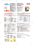
mod. IO-MB/DO-16TS
M.U. IO-MB/DO-16TS-3/09.02
Cod. J30-658-1ADO-16TS E
User manual
ISO9001 Certified
Contents
- Characteristics
- Functional Block Diagram
- Function Codes used by the module
- Diagnostics
- MODBUS Address Map organisation
- Hardware Setup
- Common parameters
- Module parameters
- Parameters Store/Restore
- Three way isolation diagram
- MODBUS Map summary
Ascon Tecnologic S.r.l.
via Indipendenza 56,
27029 - Vigevano (PV), Italia
Tel.: +39 0381 69871,
Fax: +39 0381 698730
www.ascontecnologic.com
E
MODBUS I/O module
16 Isolated
Digital Outputs
mod. IO-MB/DO-16TS
Each of the Output terminals can
be programmed as standard
optoisolated Output
APPLICABLE STANDARDS
A WARNING
The DO-16TS module is suited for the Modbus-IDA Organization protocol [1] and implements a subset of it, as explained in the text. MODBUS is a registered trademark of
Schneider Automation Inc.
The product described in this manual should only be installed, operated and maintained by
qualified application programmers and software engineers who are familiar with automation
safety concepts and applicable national standards.
Characteristics
Function Codes used by the module
Technical data
Number of channels
Polarity (EN 61131-2 type 2)
Output Voltage (nominal)
Output Current
Max. total continuous output current
ON/OFF delay
Output Single Pulse width
16
Source (PNP)
24 Vdc
0.5 A for each channel
11... 30 Vdc
5 ms
min.: 5 ms
max.: 65 s
Bit
access
Data
access
Word
access
Physical Digital Inputs
Internal Bits Or
Physical Digital
output
Physical Input Registers
Internal Registers
Or Physical Output
Registers
Read Inputs status
Read Coil status
Write Single Coil
Write Multiple Coils
Read Input Register
Read Holding Registers
Write Single Register
Write Multiple Registers
Read Exception status
Diagnostics
Diagnostics
General
3 way isolation
(see last page)
Power supply
Overvoltage protection
Dimensions
Safety regulations
EN61010-1
CE marking
Ch. to ch.: no isolation; ch. to logic: 800 Vp
serial bus to logic: 800 Vp; power supply to logic: 2.5 kVp
24 Vdc; –15...+25%
Consuption: 3 W
40 Vdc
L: 76; H: 110; W: 65;
Weight: 220g
Isolation class II (50 Vrms), Installation cathegory II
Pollution degree 2
EN61131-2
Operating
Storage
-10...+65°C
-40...+85°C
5...95% non condensing
5...95% non condensing
Relative
Appropriate measures must For a short period, slight
Humidity
be taken against
condensation may appear
humidity >85%
on the housing
Mounting
Vertical, free air
Protection
IP20
Vibrations (3 axes) 10...57Hz 0.0375mm, 57...150Hz 0.5g
Shock (3 axes)
15g, 11ms half sine
Temperature
Functional Block Diagram
02
01
05
0F
04
03
06
10
07
08
The function codes provided for all the modules are a subset of the “Public Function
Codes”, validated by the Modbus-IDA Organization.
Function 01 and Function 02 can be used to read both digital output and digital input.
Function 03 and Function 04 can be used to read both output and input registers.
Diagnostics
MODBUS Exception Responses:
Meaning
The function code received in the query is not an
allowable action for the server (or slave)
02 ILLEGAL DATA
The data address received in the query is not an
ADDRESS
allowable address for the server (or slave).
03 ILLEGAL DATA
A value contained in the query data field is not an
VALUE
allowable value for server (or slave)
07 NEGATIVE
The server (or slave) is in the wrong state to process
ACKNOWLEDGE
a request of this type or an attempt to write to a read
- NAK
only address has been made
Code 07 has not been provided by Modbus.org Protocol. Use it for ASCON products compatibility only.
Function Code 07: Read Exception Status:
bit
status
Write
state
PON or
error value
(hex)
02
01
05
15
04
03
06
16
07
08
Code Name
01 ILLEGAL FUNCTION
Environment
Receive
Functions
7
0
6
0
5
0
4
X
3
X
2
X
Discrete Input writing attempted (1)
Dummy Data Field (0 fill) (1)
Output Data Valid (1)
PON or
error mode
Function Code 08: Diagnostics
The only supported sub code is 0 – Return Query Data
1
X
0
X
Local Value status (1)
Invalid Input Data (1)
DO-16TS-uso-e
12-10-2011
13:10
Pagina 2
MODBUS Address Map organisation
Data TypeAddress RangeSub rangeData sub type
1 - 100 Physical Digital I/O
101 - 200 Digital I/O Extension
Digital I/O
1 - 400
20 - 300 Alarms
301 - 400 Status variables
1 - 120 Field/Process I/O Data
121 - 200 Device Id/Info Area
201 - 300 Field/Process I/O Extension
301 - 400 Non retentive Device Management
Registers
1 - 1200
401 - 800 Retentive Device Management
801 - 1000 Configuration Data
1001 - 1050 Diagnostics
1101 - 1200 Reserved registers
Writing and reading data length limits:
Number of Digital Outputs to be written in a single message
Max. 128
Number of Digital I/O to be read in a single message
Max. 160
Number of Output Registers to be written in a single message
Max. 16
Number of I/O Registers to be read in a single message
Max. 125
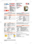
Hardware Set-up
Hexadecimal rotary switches, service and I/O LEDs
Top view
Hi
Lo
Fro
nt s
ide
LED Status
RUN Blinking
OFF
ERR Blinking
OFF
ST
Always OFF
•
•
•PWR ON
• OFF
I/O LED
Status
OUT 1...8 ON
OFF
OUT 9...16 ON
OFF
Flat blade
screwdriver
0.4 x 2.5 mm
•
•
Meaning
When in communication
Communication not present
Modbus error
No error. Device working
Module Power Supply ON
Module Power Supply OFF
Lo switch
0
1
2
3
4
5
Node ID
Baud rate
bps
300
1200
2400
4800
9600
19200
Hi
Lo
switch switch
0
1
0
2
F
7
Common Digitals
Digital outputs Name
Access
397
Parity
R/W
398
EvenOdd
R/W
Notes
0: Disabled;
1: Enabled
0: Even;
1: Odd
Output Registers Name
Access Notes
400
StackCom
R/W
Modbus Stack Command Register
Commands:
0x0
Normal State
0x5354 (ASCII code “ST”) Store Configuration in non volatile memory
0x5253 (ASCII code “RS”) Restore default configuration values
0x5254 (ASCII code “RT”) RESET (Cold Start)
Output Registers Name
801
NodeA
802
BaudR
Baud Rate
300
1200
2400
4800
9600
19200
Access
R/W
R/W
Register Value
0
1
2
3
4
5
Notes
Node Address Register
Baud Rate Register
Node Address
0 reserved
1
…
…
247
248..256 reserved
Register Value
0
1
…
…
0xF7
0xF8...0xFF
Meaning
Output active
Output not active
Output active
Output not active
Baud Rate and Node ID configuration
Baud Rate
Common parameters
Valid ID Node
1 (address 1)
2 (address 2)
0xF7 (address 247)
Module Identity Registers
Output Registers
121
122
123
124
125
126
127
Name
ManuCode
ProdCode-1
ProdCode-2
RelCode-1
RelCode-2
SpecialCode
ProdCode-3
Access
R
R
R
R
R
R
R
Notes
Manufacturer Code
Product Code # 1
Product Code # 2
Hardware Release Code
Software Release Code
Special Product Code
Product Code # 3
Access
R/W
R/W
…
R/W
Notes
User Defined Register # 1 (retentive)
User Defined Register # 2 (retentive)
...
User Defined Register # 10 (retentive)
User defined Registers
Output Registers
189
190
…
198
Name
Usr#1
Usr#2
…
Usr#10
Module parameters
Procedure for Node Address and Baud Rate configuration
The HI and LO hexadecimal rotary swithches set the module’s Baud Rate and MODBUS
Node Address. To configure the module, follow the procedure:
1 Turn the Power OFF
2 Set the HI and LO switches to “F”
3 Turn the Power ON
4 Select the desired Baud Rate value by setting the LO switch following the table
(e.g. “4” for 9600 bps)
5 Shift the HI switch to “E” (all the module service LEDs should flash)
6 Turn the Power OFF. Now configure Node ID
7 Set the HI and LO switches to the desired valid Node ID following the table
8 Turn the Power ON.
Alternatively, at step 7 set the value 00h (default value). Then, at the next Power ON, the last valid
stored value will be resumed as Node ID. The default values are: Baud Rate = 9600 bps, Node ID = 247.
Standard Outputs
Digital Outputs Name
1
DO-1
…
…
16
DO-16
Access Notes
R/W
R/W Output values
R/W
Power ON output status Register
Output Registers Name
Access Notes
Output states at Power ON
401
PO-Value
R/W
or error mode
bit
15 14 13 12 11 10 9 8 7 6 5 4 3 2 1
Channel 16 15 14 13 12 11 10 9 8 7 6 5 4 3 2
0
1
DO-16TS-uso-e
12-10-2011
13:11
Pagina 3
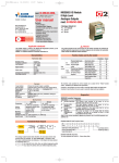
MODBUS Map summary (with default values)
Parameter Store/Restore
This module allows parameters to be saved in a non volatile memory. In order
to avoid storing configuration data parameters (registers 801...1000) by mistake, storage is only executed when a specific signature is written to the appropriate register. The signature is “ST”.
Similarly, the default values of parameters are restored. On receipt of the correct
signature in the appropriate register, the device restores the default parameters. The
signature is “RS”.
The new configuration becomes active after a reset, i.e. after a “Power Down”
or a reset command (signature “RT”). See Register 400.
es.Node address change by serial communications:
1. Write the new address in register 801 (NodeA). - Write value.
2. Write 0x5354 (ASCII code “ST”) to register 400. - Store value.
3. Write 0x5254 (ASCII code “RT”) to register 400. - Cold reset.
Modbus
address
0
...
15
396
397
Module
digital I/O
1
…
16
397
398
The retentive device management data (registers 401... 800) are immediately
valid after writing. To maintain the values after a power OFF/ON cyle, the command Store (“ST”) must be executed.
Modbus
address
120
121
122
123
124
125
126
188
189
Module
registers
121
122
123
124
125
126
127
189
190
…
198
399
400
401
801
802
197
398
399
400
800
801
Name
Access Description
DO-1
…
DO-16
Parity
EvenOdd
R/W
R/W
R/W
R/W
R/W
Name
Access Description
ManuCode
ProdCode-1
ProdCode-2
RelCode-1
RelCode-2
SpecialCode
ProdCode-3
Usr#1
Usr#2
Usr#n
Usr#8
ModuleCom
StackCom
PO_Value
NodeA
BaudR
R
R
R
R
R
R
R
R/W
R/W
R/W
R/W
RW
RW
RW
RW
RW
Logic
Output
channels
1 - 16
Manufacturer Code
Product code # 1
Product code # 2
Hardware Release Code
Software Release Code
Special Product Code # 1
Product code # 3
User Defined Register # 1
User Defined Register # 2
User Defined Register # n
User Defined Register # 8
Module Command Register
Modbus Stack Command Register
Output states at Power On
Node Address Register
Baud Rate Register
default
(hex)
0258
3136
5453
444F
FFFF
FFFF
FFFF
FFFF
0000
0000
0000
00F7
0004
A WARNING
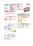
Three way isolation diagram
Serial
bus
Output 1
Output n
Output 16
0: Parity Disabled; 1: Parity Enabled
0: Parity Even; 1: Parity Odd
default
(hex)
0
0
0
0
0
The data written at retentive and configuration registers are stored in EEPROM (see “Address
Map organisation” paragraph for details). This type of memory has a limited number of writing
cycles. Also if this number is very high (about 100000 cycles), this limit can be easily reached
if the storing process is forced through a serial communications line. Please check that the
storing procedure of these registers is not performed automatically.
Power supply
2500Vp
800Vp
Reference documents
The user should refer to the following list of documents:
[1] MODBUS.ORG: MODBUS Application Protocol Specification V1.1a, June 2004
Accessories, Spare Parts and Warranty
Power Supply 45W 24Vdc 2A
Power Supply 120W 24Vdc 5A
Additional Terminal Block 2x11
Female Plug 11 Screw clamp
Female Plug 11 Spring clamp
RJ45 terminated cable 14cm
RJ45 terminated cable 22cm
Termination Adapter
AP-S2/AL-DR45-24
AP-S2/AL-DR120-24
AP-S2/TB-211-1
AP-S2/SPINA-V11
AP-S2/SPINA-M11
AP-S2/LOCAL-BUS76
AP-S2/LOCAL-BUS152
AP-S2/TERM-CAN
Warranty: 3 years excluding defects due to improper use