1
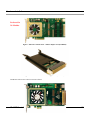
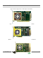
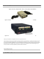
About the X6 XMC Modules
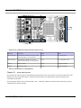
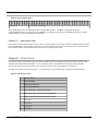
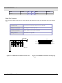
LVDS 2.5 Pins
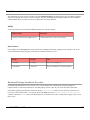
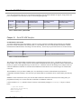
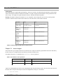
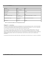
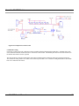
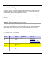
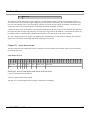
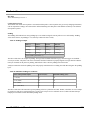
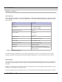
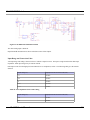
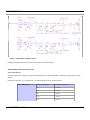
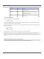
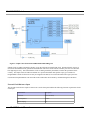
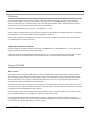
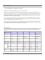
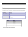
The LVDS signal pairs support high speed signaling. All pairs are routed as 100 ohm differential impedance, 50 ohm singleended. All LVDS pairs must be terminated to 100 ohms. For inputs, designers should instantiate on-chip termination in the
Virtex-6 logic. For outputs, the signal destination must have 100 ohm termination impedance.
Warning: the LVDS 2.5 DIO pins are NOT 3.3V or 5V compatible. Input voltage must not exceed 2.8V during normal
operation. Undershoot and overshoot must be limited: see the Xilinx Virtex-6 User Guide for details.
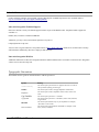
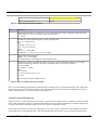
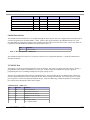
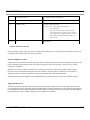
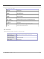
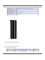
Parameter
Value
Notes
Input commonmode voltage
1.2V typical
0.3V min; 2.2V max
For differential input voltage =
+/- 350 mV
Input
Differential
Voltage
1000mV max
100mV min
100 ohm differential load
Output High
Voltage
P or N
1.765V max
100 ohm differential load
Output Low
Voltage
P or N
0.715V max
100 ohm differential load
Output
Differential
Voltage
840mV max
350mV min
100 ohm differential load
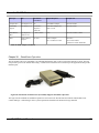
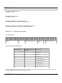
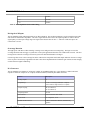
Table 16. LVDS2.5 Digital IO Bits Electrical Characteristics
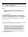
Chapter 19: Software Support
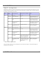
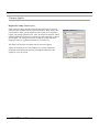
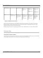
The Framework Logic configures these bit I/O connections as a simple port that has programmable bit direction and data by
the host. The port is configured and accessed directly from the PCI Express host.
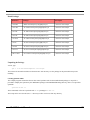
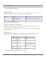
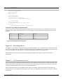
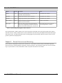
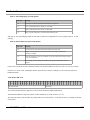
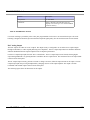
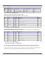
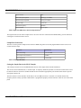
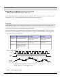
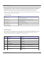
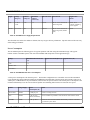
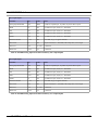
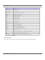
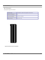
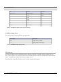
The digital I/O hardware is controlled by the IUsesDioPort class. Its properties:
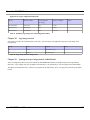
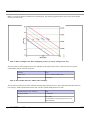
Table 17. IUsesDioPort Class Operations
Function
Type
Description
DioPortConfig()
Property
Configures banks of bits for input or output
DioPortData()
Property
Broadside Read/Write to low-order 32-bits of
DIO.
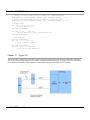
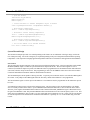
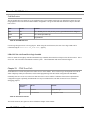
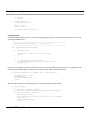
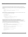
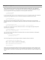
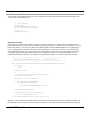
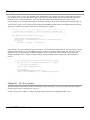
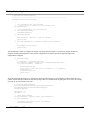
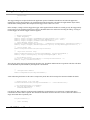
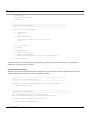
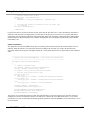
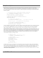
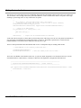
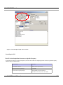
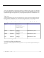
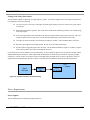
Typical use of the digital IO port involves first configuring the port using the Config() operator. This sets the byte direction and
the clock mode. The port is then ready for read/write configurations to each port. For instance:
// Open the module
X6-400M User's Manual
46