1
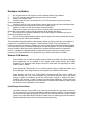
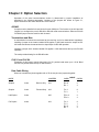
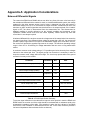
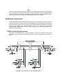
10623 Roselle Street, San Diego, CA 92121 • (858) 550-9559 • FAX (858) 550-7322
[email protected] • www.accesio.com
MODEL PCI-422/485-2
USER MANUAL
FILE: MPCI-422-485-2.A1b
Notice
The information in this document is provided for reference only. ACCES does not assume any liability
arising out of the application or use of the information or products described herein. This document may
contain or reference information and products protected by copyrights or patents and does not convey
any license under the patent rights of ACCES, nor the rights of others.
IBM PC, PC/XT, and PC/AT are registered trademarks of the International Business Machines
Corporation.
Printed in USA. Copyright 2000, 2005 by ACCES I/O Products Inc, 10623 Roselle Street, San Diego,
CA 92121. All rights reserved.
WARNING!!
ALWAYS CONNECT AND DISCONNECT YOUR FIELD CABLING
WITH THE COMPUTER POWER OFF. ALWAYS TURN COMPUTER
POWER OFF BEFORE INSTALLING A CARD. CONNECTING AND
DISCONNECTING CABLES, OR INSTALLING CARDS INTO A
SYSTEM WITH THE COMPUTER OR FIELD POWER ON MAY CAUSE
DAMAGE TO THE I/O CARD AND WILL VOID ALL WARRANTIES,
IMPLIED OR EXPRESSED.
Warranty
Prior to shipment, ACCES equipment is thoroughly inspected and tested to applicable specifications.
However, should equipment failure occur, ACCES assures its customers that prompt service and
support will be available. All equipment originally manufactured by ACCES which is found to be
defective will be repaired or replaced subject to the following considerations.
Terms and Conditions
If a unit is suspected of failure, contact ACCES' Customer Service department. Be prepared to give the
unit model number, serial number, and a description of the failure symptom(s). We may suggest some
simple tests to confirm the failure. We will assign a Return Material Authorization (RMA) number which
must appear on the outer label of the return package. All units/components should be properly packed
for handling and returned with freight prepaid to the ACCES designated Service Center, and will be
returned to the customer's/user's site freight prepaid and invoiced.
Coverage
First Three Years: Returned unit/part will be repaired and/or replaced at ACCES option with no charge
for labor or parts not excluded by warranty. Warranty commences with equipment shipment.
Following Years: Throughout your equipment's lifetime, ACCES stands ready to provide on-site or inplant service at reasonable rates similar to those of other manufacturers in the industry.
Equipment Not Manufactured by ACCES
Equipment provided but not manufactured by ACCES is warranted and will be repaired according to the
terms and conditions of the respective equipment manufacturer's warranty.
General
Under this Warranty, liability of ACCES is limited to replacing, repairing or issuing credit (at ACCES
discretion) for any products which are proved to be defective during the warranty period. In no case is
ACCES liable for consequential or special damage arriving from use or misuse of our product. The
customer is responsible for all charges caused by modifications or additions to ACCES equipment not
approved in writing by ACCES or, if in ACCES opinion the equipment has been subjected to abnormal
use. "Abnormal use" for purposes of this warranty is defined as any use to which the equipment is
exposed other than that use specified or intended as evidenced by purchase or sales representation.
Other than the above, no other warranty, expressed or implied, shall apply to any and all such
equipment furnished or sold by ACCES.
Table of Contents
Chapter 1: Introduction........................................................................................................................................ 5
Multi-Protocol Operation.................................................................................................................................. 5
RS485 and RS422 Balanced Mode Operation ................................................................................................ 5
COM Port Compatibility.................................................................................................................................... 5
Communication Modes .................................................................................................................................... 5
RTS and Auto Transceiver Control ................................................................................................................. 6
CE Mark.............................................................................................................................................................. 6
Specification...................................................................................................................................................... 7
Figure 1-1: Block Diagram.............................................................................................................................. 8
Chapter 2: Installation.......................................................................................................................................... 9
Chapter 3: Option Selection .............................................................................................................................. 11
422/485 ............................................................................................................................................................. 11
Terminations and Bias ................................................................................................................................... 11
CLK X1 and CLK X4 ........................................................................................................................................ 11
Data Cable Wiring ........................................................................................................................................... 11
Interrupts ......................................................................................................................................................... 12
In Windows NT 4 and Lower Without PCIFind.EXE..................................................................................... 12
Figure 3-1: Option Selection Map................................................................................................................. 13
Chapter 4: Address Selection ........................................................................................................................... 14
Chapter 5: Programming ................................................................................................................................... 15
Sample Programs............................................................................................................................................ 15
Windows Programming.................................................................................................................................. 15
Initialization ..................................................................................................................................................... 15
Table 5-1: Baud Rate Divisors...................................................................................................................... 16
Reception......................................................................................................................................................... 17
Transmission................................................................................................................................................... 17
Chapter 6: Connector Pin Assignments .......................................................................................................... 19
Table 6-1: Connector Pin Assignments ........................................................................................................ 19
Appendix A: Application Considerations......................................................................................................... 20
Balanced Differential Signals ........................................................................................................................ 20
Table A-1: RS422 Specification Summary ................................................................................................... 20
RS485 Data Transmission.............................................................................................................................. 21
RS485 Two-Wire Multidrop Network ............................................................................................................. 21
Figure A-1: Typical RS485 Two-Wire Multidrop Network ............................................................................ 21
RS485 Four-Wire Multidrop Network ............................................................................................................ 22
Chapter 1: Introduction
This Serial Communications Card was designed for use in PCI-Bus computers and provides
two serial ports for effective communication in the most common protocols. The card is 6.15
inches long (156 mm) and may be installed in any 5-volt PCI slot in IBM or compatible
computers.
Multi-Protocol Operation
These are dual-protocol serial cards that support RS422 and RS485 communications. RS422
uses differential (or balanced) line drivers to improve noise immunity and increase the
maximum distance to 4000 feet. RS485 improves on RS422 with switchable transceivers and
the ability to support multiple devices on a single "party line". The RS485 specification defines a
maximum of 32 devices on a single line. The number of devices served on a single line can be
expanded by use of "repeaters".
RS485 and RS422 Balanced Mode Operation
The cards support RS422 and RS485 modes which use differential balanced drivers for
increased range and noise immunity. The card also has capability to add bias voltages and to
add load resistors to terminate the communications lines. RS485 communications requires that
one transmitter supply a bias voltage to ensure a known "zero" state when all transmitters are
off. Also, receiver inputs at each end of the network should be terminated to eliminate "ringing".
These cards support these options by means of jumpers on the card. See the "Option
Selection" section of this manual for more details.
COM Port Compatibility
Type 16550 UARTs are used as the Asynchronous Communication Element (ACE). These
include a 16-byte transmit/receive FIFO buffer to protect against lost data in multitasking
operating systems, while maintaining 100% compatibility with the original IBM serial port. PCI
bus architecture allows addresses between 0000 and FFF8 hex to be assigned to the cards.
PCIFind.EXE is a utility provided to determine the base addresses assigned by the system.
A crystal oscillator is located on the card. This oscillator permits selection of baud rates up to
115,200. Rates up to 460,800 baud (4X UART clock) are available by jumper selection.
The driver/receiver used, the 75176, is capable of driving extremely long communication lines
at high baud rates. It can drive up to +60 mA on balanced lines and receive inputs as low as
200 mV differential signal superimposed on common mode noise of +12 V or -7 V. In case of
communication conflict, the driver/receivers feature thermal shutdown.
Communication Modes
The cards support Half-Duplex, and Full-Duplex communications in 2- and 4-wire cable
connections. Half-Duplex allows traffic to travel in both directions, but only one way at a time. In
Full-Duplex operation, data travels in both directions at the same time. RS485 communications
use the half-duplex mode because only a single pair of wires need to be used and installation
costs are dramatically reduced.
RTS and Auto Transceiver Control
In RS485 communications the driver must be enabled and disabled as needed, allowing all
cards to share a two wire cable. This card provides automatic control, where the driver is
enabled when data is ready to be transmitted. The driver remains enabled for the transmission
time of one additional character after data transfer is complete and then is disabled. The cards
automatically adjust their timing to the baud rate of the data.
The receiver is also normally disabled during RS485 transmissions.
CE Mark
If your card is CE-marked, it meets the requirements of EN50081-1:1992 (Emissions),
EN50082-1:1992 (Immunity), and EN60950:1992 (Safety).
Specification
Communications Interface
•
Serial Ports:
Shielded male D-sub 9-pin IBM AT style connectors
compatible with RS422 and RS485 specifications.
•
Character length:
5, 6, 7, or 8 bits.
•
Parity:
Even, odd or none.
•
Stop Interval:
1, 1.5, or 2 bits.
•
Serial Data Rates:
Up to 115,200 baud, asynchronous. A faster range of rates, up
to 460,800 baud, is achieved by jumper selection on the card.
Type 16550 buffered UART.
Caution
The OUT2 bit of the UART must be set low for proper interrupt driven communication. This bit enables
or disables the interrupts and the card will not communicate if the bit is pulled high.
Differential Communication Mode
•
Multipoint:
Compatible with RS422 and RS485 specifications. Up to 32
drivers and receivers allowed on line. Serial communications
ACE used is type 16550. Driver/Receivers used are type
75176.
•
Receiver Input Sensitivity:
+200 mV, differential input.
•
Common Mode Rejection:
+12V to -7V
•
Transmitter Output Drive Capability:
60 mA.
Environmental
•
Operating Temperature Range: 0 °C. to +60 °C.
•
Storage Temperature Range:
-50 °C. to +120 °C.
•
Humidity:
5% to 95%, non-condensing.
•
Power Required:
+5VDC at 125 mA typical, +12VDC at 5 mA typical, 685 mW
total power consumption.
•
Size:
6 1/2" long (165 mm) by 3 7/8" (98 mm).
CO MPUTER PCI BUS
OSCILLATOR
Tx
PCI
Tx/Rx+
UART
16550
OR
SIMILAR
INTERFACE
CHIP
DB9M
TRANSCEIVER
Tx/RxRx
IRQ
AUTO RTS
CIRCUITRY
RS485 MODE
ONLY
TYPICAL OF 2
Figure 1-1: Block Diagram
Chapter 2: Installation
A printed Quick-Start Guide (QSG) is packed with the card for your convenience. If you’ve already
performed the steps from the QSG, you may find this chapter to be redundant and may skip forward to
begin developing your application.
The software provided with this card is on CD and must be installed onto your hard disk prior to use. To
do this, perform the following steps as appropriate for your operating system.
CD Software Installation
The following instructions assume the CD-ROM drive is drive “D”. Please substitute the appropriate
drive letter for your system as necessary.
DOS
1.
2.
3.
4.
Place the CD into your CD-ROM drive.
Type B- to change the active drive to the CD-ROM drive.
Type GLQR?JJ- to run the install program.
Follow the on-screen prompts to install the software for this board.
WINDOWS
1.
Place the CD into your CD-ROM drive.
2.
The system should automatically run the install program. If the install program does not run
promptly, click START | RUN and type BGLQR?JJ, click OK or press -.
3.
Follow the on-screen prompts to install the software for this board.
LINUX
1.
Please refer to linux.htm on the CD-ROM for information on installing under linux.
Caution! * ESD A single static discharge can damage your card and cause premature
failure! Please follow all reasonable precautions to prevent a
static discharge such as grounding yourself by touching any
grounded surface prior to touching the card.
Hardware Installation
1.
Do not install card into the computer until the software has been fully installed.
2.
Turn OFF computer power AND unplug AC power from the system.
3.
Remove the computer cover.
4.
Carefully install the card in an available 5V or 3.3V PCI expansion slot (you may need to
remove a backplate first).
5.
Inspect for proper fit of the card and tighten screws. Make sure that the card mounting bracket
is properly screwed into place and that there is a positive chassis ground.
6.
Install an I/O cable onto the card’s bracket mounted connector.
7.
Replace the computer cover and turn ON the computer which should auto-detect the card
(depending on the operating system) and automatically finish installing the drivers.
8.
Run PCIfind.exe to complete installing the card into the registry (for Windows only) and to
determine the assigned resources.
9.
Run one of the provided sample programs that was copied to the newly created card directory
(from the CD) to test and validate your installation.
The base address assigned by BIOS or the operating system can change each time new hardware is
installed into or removed from the computer. Please recheck PCIFind or Device Manager if the
hardware configuration is changed. Software you write can automatically determine the base address
of the card using a variety of methods depending on the operating system. In DOS, the PCI\SOURCE
directory shows the BIOS calls used to determine the address and IRQ assigned to installed PCI
devices. In Windows, the Windows sample programs demonstrate querying the registry entries
(created by PCIFind and NTIOPCI.SYS during boot-up) to determine this same information.
Windows COM Numbers
Under Windows 9x, the card will typically install as COM5 and COM6. Using Device Manager,
these assignments can be changed to any available COM number greater than COM4;
limitations in the Microsoft COM drivers prevent PCI COM ports from appearing as COM1,
COM2, COM3, or COM4.
Under Windows NT 2000 and NT XP, the card will typically install as COM3 and COM4. Using
Device Manager, these assignments can be changed to any available COM number.
Under Windows NT4 and lower, PCIFind.EXE will typically install the card as COM5 and
COM6. Because this is not a PNP-compliant OS, PCIFind.EXE will place itself in the system
registry to update the installation should the card move(for example, if another PCI card is
installed) or be removed. In order to change the COM number assignment, PCIFind.EXE must
be removed from the registry(which will also sacrifice its pseudo-PNP behavior); please contact
the factory for further assistance if this is desired.
Input/Output Connections
Two DB9 connectors are provided on the card mounting bracket for input/output connections.
To ensure that there is minimum susceptibility to EMI and minimum radiation, it is important that
the card mounting bracket be properly screwed into place and that there be a positive chassis
ground. Also, proper EMI cabling techniques (cable connect to chassis ground at the aperture,
shielded twisted-pair wiring, etc) be used for the input/output wiring.
Chapter 3: Option Selection
Operation of the serial communications section is determined by jumper installation as
described in the following paragraphs. Locations of the jumpers are shown in Figure 3-1,
Option Selection at the end of this section of the manual.
422/485
Jumpers must be installed in these blocks for each COM port. The function of the 422 and 485
jumpers is to configure the port for RS-422 or RS-485 mode communications. Either an RS-422
or RS-485 jumper must be used for each channel.
Terminations and Bias
A transmission line should be terminated at the receiving end in its characteristic impedance.
Installing a jumper at the location labeled LDO applies a 120Ω load across the output for RS422 mode and across the transmit/receive input/output for RS-485 operation.
Installing a jumper at the location labeled LDI applies a 120Ω load across the input for RS-422
operation.
The card provides biasing for the RS-485 mode.
CLK X1 and CLK X4
Placement of this jumper controls baud rate. CLK X1 permits baud rates up to 115.2K Baud
and CLK X4 permits baud rates up to 460.8K Baud.
Data Cable Wiring
When two numbers are joined together with a "&" the two pins are jumpered together.
CABLE
MODE
JUMPERS
CARD1
CARD2
Simplex
2-wire
Receive Only
422
Rx+ 9
Rx- 1
2
3
Simplex
2-wire
Transmit Only
422
Tx+ 2
Tx- 3
9
1
Half Duplex
2-wire
485
TRx+ 2
TRx- 3
2
3
Full Duplex
4-wire
422
Tx+ 2
Tx- 3
Rx+ 9
Rx- 1
9
1
2
3
Interrupts
Use PCIFind.EXE to determine the IRQ that was assigned to the card by the BIOS or Operating
System. Alternatively, in Windows 9x or NT2000, the Device Manager can be used. The PCI422/485-2’s ports are listed under the Ports class. Selecting the port, clicking Properties, then
selecting the Resources tab will show the base addresses and IRQ assigned to the port.
In Windows NT 4 and Lower Without PCIFind.EXE
In Windows NT, changes must be made to the system registry to support IRQ sharing.
PCIFind.EXE normally detects the COM boards in the system and makes these changes, but if
PCIFind.EXE will not be run or is working improperly for some reason, these changes must be
made manually. The following is excerpted from "Controlling Multiport Serial I/O Cards"
provided by Microsoft in the MSDN library, documentid:mk:@ivt:nt40res/D15/S55FC.HTM, also
available in the WindowsNT Resource Kit. The text enclosed in brackets ("[ ]") denotes a
comment by the editors.
The Microsoft serial driver can be used to control many dumb multiport serial cards. Dumb
indicates that the control includes no on-board processor. Each port of a multiport card has a
separate subkey under the CurrentControlSet\Services\Serial subkey in the registry. In each of
these subkeys, you must add values for DosDevices, Interrupt, InterruptStatus,
PortAddress, and PortIndex because these are not detected by the Hardware Recognizer.
(For descriptions and ranges for these values, see Regentry.hlp, the Registry help file on the
WindowsNT Workstation Resource Kit CD.)
For example, if you have a four-port COM card configured to use address 0xFFF0 with an
interrupt of 0xFFF8, the values in the Registry are: [assuming that every port is configured to
use the same IRQ and that the addresses are configured to be consecutive and contiguous]
Serial2 Subkey:
PortAddress = REG_DWORD 0xFFF0
Interrupt = REG_WORD 5
DosDevices = REG_SZ COM3
InterruptStatus = REG_DWORD 0xFFF8
PortIndex = REG_DWORD 1
Serial4 Subkey:
PortAddress = REG_DWORD 0xFF90
Interrupt = REG_DWORD 5
DosDevices = REG_SZ COM5
InterruptStatus = REG_DWORD 0xFFF8
PortIndex - REG_DWORD 3
Serial3 Subkey:
PortAddress = REG_DWORD 0xFFE0
Interrupt = REG_DWORD 5
DosDevices = REG_SZ COM4
InterruptStatus = REG_DWORD 0xFFF8
PortIndex = REG_DWORD 2
Serial5 Subkey:
PortAddress = REG_DWORD 0xFF80
Interrupt = REG_DWORD 5
Dos Devices = REG_SZ COM6
InterruptStatus = REG_DWORD 0xFFF8
PortIndex = REG_DWORD 4
R S 422
LD I
LD O
A
R S 422
Figure 3-1: Option Selection Map
Jumpers
RS422:
RS485-A, RS485-B:
LDO:
LDI:
X1/X4:
Select differential(RS-422, four-wire) communications mode
Select differential(RS-485, two-wire) communications mode
Apply load to RS-422 output or RS-485
Apply load to RS-422 input
Select either 115.2 Kbaud or 460.8 Kbaud maximum
RS485-A
LD O
RS485-B
B
X4
X1
LD I
Chapter 4: Address Selection
The card uses two separate address spaces, each occupying eight consecutive register
locations, for COM A and COM B, respectively. PCI architecture is Plug-and-Play. This means
the BIOS or Operating System determines the resources assigned to PCI cards, rather than
you selecting these resources with switches or jumpers. As a result, the card's base address
cannot be changed, it can only be determined.
To determine the base address that has been assigned to the card, run the provided
PCIFind.EXE utility program (PCINT.EXE for Windows95 systems.). This utility will display a list
of all of the ACCES cards detected on the PCI bus, the addresses assigned to each function on
each of the cards, and the respective IRQs and DMAs (if any) allotted.
Alternatively, some operating systems (Windows 95/98/2000) can be queried to determine
which resources were assigned. In these operating systems, you can use either PCIFind or the
Device Manager utility from the System Properties Applet of the control panel. These cards are
installed in the Data Acquisition class of the Device Manager list. Selecting the card then
clicking Properties, then selecting the Resources Tab will display a list of the resources
allocated to the card.
PCIFind uses the Vendor ID and the device ID to search for your card, then reads the base
address and IRQ assigned. If you want to determine the base address and IRQ assigned, use
the following information:
The Vendor ID code for this card is 494F (ASCII for "I/O").
The Device ID code for the card is 1150
PCI supports 64 K of address space, so your card's addresses may be located anywhere in the
0000 to FFF8 hex range.
Chapter 5: Programming
Sample Programs
There are sample programs provided with the card in C, Pascal, QuickBASIC, and several
Windows languages. DOS samples are located in the DOS directory and Windows samples are
located in the WIN32 directory.
Windows Programming
The card installs into Windows as COM ports. Thus the Windows standard API functions can
be used. In particular:
► CreateFile() and CloseHandle() for opening and closing a port.
► SetupComm(), SetCommTimeouts(), GetCommState(), and SetCommState() to set
and change a port’s settings.
► ReadFile() and WriteFile() for accessing a port.
See the documentation for your chosen language for details.
Under DOS, the process is very different. The remainder of this chapter describes DOS
programming.
Initialization
Initializing the chip requires knowledge of the UART's register set. The first step is to set the
baud rate divisor. You do this by first setting the DLAB (Divisor Latch Access Bit) high. This bit
is Bit 7 at Base Address +3. In C code, the call would be:
outportb(BASEADDR +3,0x80);
You then load the divisor into Base Address +0 (low byte) and Base Address +1 (high byte).
The following equation defines the relaionship between baud rate and divisor:
Desired Baud Rate = (UART clock frequency) ÷ (32 divisor)
When the BAUD jumper is in the X1 position, the UART clock frequency is 1.8432MHz. When
the jumper is in the X4 position, the clock frequency is 7.3728 MHz. The following table lists
popular divisor frequencies. Note that there are two columns to consider depending on the
position of the BAUD jumper.
Baud Rate
460800
230400
153600
115200
57600
38400
28800
19200
14400
9600
4800
2400
1200
Divisor x1
1
2
3
4
6
8
12
24
48
96
Divisor x4
1
2
3
4
8
12
16
24
32
48 – Most Common
96
192
384
Max Diff. Cable Length*
550 ft
1400 ft
2500 ft
3000 ft
4000 ft
4000 ft
4000 ft
4000 ft
4000 ft
4000 ft
4000 ft
4000 ft
4000 ft
* Recommended maximum distances for differentially driven data cables (RS422 or RS485) are for typical conditions.
Table 5-1: Baud Rate Divisors
In C, the code to set the chip to 9600 baud is:
outportb(BASEADDR, 0x0C);
outportb(BASEADDR +1,0);
The second initializing step is to set the Line Control Register at Base Address +3. This register
defines word length, stop bits, parity, and the DLAB.
Bits 0 and 1 control word length and allow word lengths from 5 to 8 bits. Bit settings are
extracted by subtracting 5 from the desired word length.
Bit 2 determines the number of stop bits. There can be either one or two stop bits. If Bit 2 is
set to 0, there will be one stop bit. If Bit 2 is set to 1, there will be two stop bits.
Bits 3 through 6 control parity and break enable. They are not commonly used for
communications and should be set to zeroes.
Bit 7 is the DLAB discussed earlier. It must be set to zero after the divisor is loaded or else
there will be no communications.
The C command to set the UART for an 8-bit word, no parity, and one stop bit is:
outportb(BASEADDR +3, 0x03)
The third step of the initialization sequence is to set the Modem Control Register at Base
Address +4. Bit 1 is the Request to Send (RTS) control bit. This bit should be left low until
transmission time. (Note: When operating in the automatic RS485 mode, the state of this bit is
not significant.) Bits 2 and 3 are user-designated outputs. Bit 2 may be ignored on this card. Bit
3 is used to enable interrupts and should be set high if an interrupt-driven receiver is to be
used.
The final initialization step is to flush the receiver buffers. You do this with two reads from the
receiver buffer at Base Address +0. When done, the UART is ready to use.
Reception
Reception can be handled in two ways: polling and interrupt-driven. When polling, reception is
accomplished by constantly reading the Line Status Register at Base Address +5. Bit 0 of this
register is set high whenever data are ready to be read from the chip. A simple polling loop
must continuously check this bit and read in data as it becomes available. The following code
fragment implements a polling loop and uses a value of 13, (ASCII Carriage Return) as an endof-transmission marker:
do{
while (!(inportb(BASEADDR +5) & 1));
data[i++]= inportb(BASEADDR);
}while (data[i]!=13);
/*Wait until data ready*/
/*Reads the line until null character rec'd*/
Interrupt-driven communications should be used whenever possible and is required for high
data rates. Writing an interrupt-driven receiver is not much more complex than writing a polled
receiver but care should be taken when installing or removing your interrupt handler to avoid
writing the wrong interrupt, disabling the wrong interrupt, or turning interrupts off for too long a
period.
The handler would first read the Interrupt Identification Register at Base Address +2. If the
interrupt is for Received Data Available, the handler then reads the data. If no interrupt is
pending, control exits the routine. A sample handler, written in C, is as follows:
readback = inportb(BASEADDR +2);
if(readback & 4)
data[i++] = inportb(BASEADDR);
outportb(0x20,0x20);
return;
/*Readback will be set to 4 if data are
available*/
/*Write EOI to 8259 Interrupt Controller*/
Transmission
The Auto feature of the PCI-422/485-2 card automatically enables the transmitter when data
are ready to send so no software enabling is required. The following software example is for
non-Auto operation.
First the RTS line should be set high by writing a 1 to Bit 1 of the Modem Control Register at
Base Address +4. The RTS line is used to toggle the transceiver from receive mode to transmit
mode and vice versa. It is not carried out on the line in RS485 and is not used for handshaking.
Similarly, the CTS line is not used in RS485 and should always be enabled by installing a
jumper as described earlier.
After the above is done, the card is ready to send data. To transmit a string of data, the
transmitter must first check Bit 5 of the Line Status Register at Base Address +5. That bit is the
transmitter-holding-register-empty flag. If it is high, the transmitter has sent the data. The
process of checking the bit until it goes high followed by a write is repeated until no data
remains. After all data has been transmitted, the RTS bit should be reset by writing a 0 to Bit 1
of the Modem Control Register.
The following C code fragment demonstrates this process:
outportb(BASEADDR +4, inportb(BASEADDR +4)|0x02);
/*Set RTS bit without altering states of other bits*/
while(data[i]); /*While there is data to send*/
{
while(!(inportb(BASEADDR +5)&0x20)); /*Wait until transmitter is empty*/
outportb(BASEADDR,data[i]);
i++;
}
outportb(BASEADDR +4, inportb(BASEADDR +4)&0xFD);
/*Reset RTS bit without altering states of other bits*/
Caution
The OUT2 bit of the UART must be set low for proper interrupt driven communication. This bit
enables or disables the interrupts and the card will not communicate if the bit is pulled high.
Chapter 6: Connector Pin Assignments
The popular 9-pin D subminiature connector is used for interfacing to communication lines. The
connector is equipped with 4-40 threaded standoffs (female screw lock) to provide strain relief.
Pin No.
RS422 Functions
RS485 Functions
1
Rx- Receive Data
2
Tx+ Transmit Data
TRx+ Transmit/Receive Data
3
Tx- Transmit Data
TRx- Transmit/Receive Data
GND Ground
GND Ground
4
5
6
7
8
9
Rx+ Receive Data
Table 6-1: Connector Pin Assignments
Note
If connections are to be made to a CE-marked version, then CE-certifiable cabling and
breakout methodology (Cable shields connected to ground at the mounting bracket shielded
twisted-pair wiring, etc) must be used.
Appendix A: Application Considerations
Balanced Differential Signals
The reason that RS422 and RS485 devices can drive long lines with more noise immunity is
that a balanced differential drive method is used. In a balanced differential system, the voltage
produced by the driver appears across a pair of wires. A balanced line driver will produce a
differential voltage from +2 to +6 volts across its output terminals. A balanced line driver can
also have an input "enable" signal that connects the driver to its output terminals. If the "enable"
signal is OFF, the driver is disconnected from the transmission line. This disconnected or
disabled condition is usually referred to as the "tristate" condition and represents a high
impedance. RS485 drivers must have this control capability. RS422 drivers may have this
control but it is not always required.
A balanced differential line receiver senses the voltage state of the transmission line across the
two signal input lines. If the differential input voltage is greater than +200 mV, the receiver will
provide a specific logic state on its output. If the differential voltage input is less than -200 mV,
the receiver will provide the opposite logic state on its output. The maximum operating voltage
range is from +6V to -6V allowing for voltage attenuation that can occur on long transmission
cables.
A maximum common mode voltage rating of +7V provides good noise immunity from voltages
induced on the twisted pair lines. The signal ground line connection is necessary in order to
keep the common mode voltage within that range. The circuit may operate without the ground
connection but may not be reliable.
Parameter
Conditions
Driver Output Voltage (unloaded)
Driver Output Voltage (loaded)
Min.
Max.
4V
6V
-4V
-6V
LDO
2V
jumpers in
-2V
Driver Output Resistance
50Ω
Driver Output Short-Circuit Current
+150 mA
Driver Output Rise Time
10% unit interval
Receiver Sensitivity
+200 mV
Receiver Common Mode Voltage Range
+7V
Receiver Input Resistance
4KΩ
Table A-1: RS422 Specification Summary
To prevent signal reflections in the cable and to improve noise rejection in both the RS422 and
RS485 mode, the receiver end of the cable should be terminated with a resistance equal to the
characteristic impedance of the cable. (The exception is when the line is driven by an RS422
driver that is never "tristated" or disconnected from the line. In this case, the driver provides a
low internal impedance that terminates the line at that end.)
Note
You do not have to add a terminator resistor to your cables when you use the PCI-422/485-2
card. Termination resistors for the RX+ and RX- lines are provided on the card and are placed
in the circuit when you install the termination jumpers. Moreover, installing the BIAS jumpers
properly biases these lines. (See the Option Selection section of this manual.)
RS485 Data Transmission
The RS485 Standard allows a balanced transmission line to be shared in a party-line mode. As
many as 32 driver/receiver pairs can share a two-wire party line network. Many characteristics
of the drivers and receivers are the same as in the RS422 Standard. One difference is that the
common mode voltage limit is extended and is +12V to -7V. Since any driver can be
disconnected (or tristated) from the line, it must withstand this common mode voltage range
while in the tristate condition.
RS485 Two-Wire Multidrop Network
The following illustration shows a typical multidrop or party line network. Note that the
transmission line is terminated on both ends of the line but not at drop points in the middle of
the line.
Figure A-1: Typical RS485 Two-Wire Multidrop Network
RS485 Four-Wire Multidrop Network
An RS485 network can also be connected in a four-wire mode. In a four-wire network it's
necessary that one node be a master node and all others be slaves. The network is connected
so that the master communicates to all slaves and all slaves communicate only with the master.
This has advantages in equipment that uses mixed protocol communications. Since the slave
nodes never listen to another slave's response to the master, a slave node cannot reply
incorrectly.
Customer Comments
If you experience any problems with this manual or just want to give us some feedback, please
email us at: [email protected].. Please detail any errors you find and include your
mailing address so that we can send you any manual updates.
10623 Roselle Street, San Diego CA 92121
Tel. (858)550-9559 FAX (858)550-7322
www.accesio.com