1
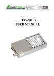
FC-301/D USER MANUAL SHENZHEN FRIENDCOM TECHNOLOGY DEVELOPMENT CO.,LTD ADD: 6/F, 17 Building , Guangqian Industrial Park, Longzhu Road, Xili Town, Nanshan, Shenzhen City 518055 P.R.CHINA. TEL: +86-755-86026600 +86-755-86026192 FAX: +86-755-86026300 E-MAIL : [email protected] WEBSITE: www.friendcom.cn TABLE OF CONTENTS TABLE OF CONTENTS ...................................... 01 .. SPECIFICATIONS ..........................................02 CIRCUIT DIAGRAM........................................07 INTRODUCTION...........................................08 FEATURES................................................08 TROUBLE SHOOTING GUIDE...............................09 WIRING DIAGRAM.........................................10 PROGRAMMING ..........................................13 FACTORY DEFAULT SETTING ..............................27 -1- SPECIFICATION GENERAL Equipment Type…………………………………Data Radio Performance Specification…………..................TIA/EIA-603 & ETS 300-113 Band …………………………………………...UHF/VHF Channel Spacing………………………………25KHz,12.5KHz programmable RF Output Power……………………………….1W - 5W Programmable Modulation type ………………………………..16K0F3E,8K5F3E Intermediate Frequency………………………… 45.1MHz & 455KHz Number of Channels…………………………….16 Frequency Source ……………………………….Synthesizer Operation Rating…………………………………Intermittent 5:5:90 ( TX: RX: Standby ) Power Supply ……………………………………12.5V DC Nominal Voltage Temperature Range Storage………………………………………from –40°C to +80°C Operating……………………………………from –30°C to +60°C Current Consumption Standby (Muted) ……………………………≤40mA Transmit 5 Watts RF Power …………………< 1.5A Transmit 1 Watt RF Power…………………..<0.8A -2- Frequency Bands ………………RX ………………TX UHF: 400 – 470 MHz VHF: 136 – 174 MHz UHF: 400 – 470 MHz VHF: 136 – 174 MHz Dimensions………………………………………..(120mm)L x (60mm)W x (20mm)H Weight……………………………………………..≤150 grams TRANSMITTER Sustained Transmission…………………………… Nominal conditions Time: 5 10 Power: >95% >95% 30 sec >90% Frequency Error…………………………………..±2.5 ppm Frequency Deviation: 25kHz Channel Spacing……………………..≤±5.0kHz, 12.5kHz Channel Spacing……………………≤±2.5kHz, Audio Frequency Response………………………. Within +1/-3dB of 6dB octave @300Hz to 2.55kHz for 12.5kHz C.S @300Hz to 3.0khz for 25kHz C.S Adjacent Channel Power 25kHz…………………………………………< 70 dBc @ Nominal Condition <65 dBc @ Extreme Condition 12.5kHz ………………………………………< 60 dBc @ Nominal Condition < 55 dBc @ Extreme Condition Conducted Spurious Emission …………………….< -36 dBM Modulation Sensitivity……………………………. 100mV RMS@60% peak Dev. Hum & Noise: 25kHz Channel Spacing………………….….>40 dB (with no PSOPH) -3- 12.5kHz Channel Spacing………………..……>36 dB (with POSPH) Modulation Symmetry ……………………………..<10% Peak Dev@1kHz input for nominal dev +20dB Load Stability……………………………………No osc at >= 10:1 VSWR all phase angles and suitable antenna No destroy at >= 20:1 all phase angle RECEIVER Sensitivity(12dB Sinad) ………………………….UHF <-117 dBm, VHF<[email protected] Amplitude Characteristic………………………….<±3dB Adjacent Channel Selectivity: 25 kHz Channel Spacing …………………….≥70dB @ Nom. 12.5kHz Channel Spacing…………………….≥60dB@Nom. Spurious Response Rejection………………………70dB Image Response…………………………………… > 70 dB IF Response ………………………………………. >70 dB Others………………………………………………> 70 dB Intermodulation Response Rejection………………≥65 dB Conducted Spurious Emission @ Nominal Conditions………<-57 dBm AF Distortion ………………………………………………....<5% @ Nom., <10%@ Extreme Condition RX Hum & Noise: 25.0kHz CP……………………………………………< 40dB No PSOPH 12.5kHz CP ………………………………………..…< 40dB with PSOPH -4- Receiver Response Time …………………………….< 20ms Squelch Opening sensitivity: ………………………-118dBm Squelch Closing sensitivity ……………………….. -121dBm Squelch Attack Time: RF Level at Threshold ………………………… <40ms RF Level at Threshold +20dB…………………<30ms L.O. Frequency Temperature Stability…………….1 st <2.5 ppm, 2 nd <10 ppm for –30°C to +60°C L.O. Frequency Aging Rate………………………….±2 ppm/year REFERENCE CRYSTAL Frequency…………………………………………………. 13MHz Temperature Characteristic……………………………+/- 2.5PPM from –30°C to +60°C Aging Rate……………………………………………….< 2ppm/year in 1 st year <1ppm/year thereafter Lock Time …………………………………………………<10 ms TX to RX ………………………………………………… < 20 ms RX to TX ………………………………..……………….. < 25 ms ENVIRONMENTAL ( performance without degradation unless stated) Temperature……………………………………………… deg C Operating………………………………………………….-30° to +60°C Degradation Specified@Extreme Storage …………………………………………………… -40°C to +80°C -5- Recharging ……………………………………………… -10 to +55 ESD………………………………………………………. 20kV (C-MIC >= 15kV) Vibration………………………………………………… MIL STD 810 C Procedures I,II,V and IEC68 26 ·Due to continuing researching and development the company reserves the right to alter these specifications without prior notice. -6- FC-301/D CIRCUIT DIAGRAM Fig.1. Circuit diagram -7- INTRODUCTION The FC-301/D Series of RF Link Modules from Friendcom utilizes the latest technology in its design and manufacturing. Both the UHF and VHF models are PLL (Phase Lock Loop Synthesizer) / microprocessor controlled, and offer one to five watts of power with 16 channel capability. Multiple functions including AC audio coupling, 1200 to 9600 baud rates GMSK and FSK modulation capability are standard in these fully programmable wide bandwidth RF Link Module units. FEATURES ● 16 Channels ●1- 5 Watt Programmable Output ●12.5 / 25 kHz Programmable Channel Spacing -8- TROUBLE SHOOTING GUIDE Table 1: Trouble shootings SYMPTOM S Unit does not work Bad RX Sensitivity CAUSES 1.No power incomplete connection 2. No input voltage of 5V or 8V 3. CPU does not work 4. EEPROM fail 5. Channel error 6. PLL error 1.Antenna signal short-circuit 2.Antenna signal open-circuit 3. Bad electronic turner 4. Defective high frequency amplifier 5. Bad mixer 6. Local signal amplitude become small 7. Bad 1st and 2nd intermediate COUNTERMEASURES 1.Check COM1 connection 2. Check IC500、IC504 3. Check IC510 4. Check IC502 5. Check CF3 6. Check TCXO、VCO、PLL IC 1. Check D106 D107 2. Antenna loose weld 3. Check L23 L24 L25 L26 4. Replace Q15 5. Check IC3 T3 T4 6. Check D103 Q111 7. Check XF1 XF2 IC2 frequency Defective RX 1. No output signal 2. Bad signal waveform 3. Bad stability of VCO 1. Replace IC801 2. Check U2 c412 c404 3. Check component of VCO PLL Error 1. TCXO frequency error 2. Bad stability of VCO 3. PLL can’t be locked 1.Check crystal oscillator of TCXO 2.Check the component of TX/RXVCO 3. IC301 Q321 Q320 C327 Low TX Power 1. Bad amplifier circuit 2. Bad APC circuit 1. Replace IC102 2. Check D102 IC1 No TX Power 1. No power on TX 2. No signal on driver 3. Bad amplifier circuit 4. Bad APC circuit 1. Check Q502 Q503 2. Check Q1 Q2 D101 3. Check IC102 D102 4. Check IC1 No Modulation 1. No input signal 2. No TX signal 1. Check IC801 2. Check U1 R403 R404 -9- WIRING DIAGRAM The standard FC-301/D is shown as below picture. The pins of CON1, CON2 and CON3 are all connected via the bridge board (As shown in Fig.2 and Fig.3). Fig.2. FC-301/D with bridge board - 10 - Fig.3. Wiring diagram - 11 - Table2 : Pin Description Pin Function Type Pin 1 Audio TX) Pin 2 Audio out (Data Output RX ) 150mV-250mV Demodulation Output Pin 3 PTT 0 V/+5V in(Data Input Input Range 200mVP-P 300mVP-P Description ------ External Modulation Input Transmit Enable 0V - Radio in Transmit status 5V Radio status(Default ) in receive Pin 4 GND GND 0V GND Pin 5 B+ V+ 10-15V Power Supply(+12.5V typical ) Output Open/Short RF Carrier Detect Pin 6 SQ Open -- low level, Short -- high level (Default). Pin 7 RSSI Pin 8 Switch Output 0.8V-2.2V Input 0V/5V Programming Enable 0V - Radio programmable 5V - Radio work (Default ) Pin 9 Speaker Output 8ohm /0.5W - 12 - PROGRAMMING When you want to program FC-301/D, you should connect the radio with the program cable (TTL to RS-232) to PC as shown in below Fig. 4.: Fig.4. Program cable of FC-301/D And the radio should be connected with the bridge board as shown in Fig.2. FC-301/D should be connected with PC via program cable as Fig.4. when in program mode. The detailed description as below: Red wire (Pin 5): Power supply +12.5V, Black wire (Pin 4): Power negative (GND). Yellow wire(Pin 8): GND. (Yellow wire to GND for program, hung for - 13 - normal work mode). Run program software ‘QuickSet.exe’ for FC-301/D to program the radio. The detailed procedures on programming FC-301/D as following: Ⅰ. To start FC-301/D Program Software and read the parameters of FC-301/D RF Link Module Step 1: Make sure the radio FC-301/D is in program status (pin8 SW of CON1(DB9) in low level-GND) and the connection is ready between FC-301/D and PC via program cable. Step 2: Double click ‘QuickSet.exe’ for FC-301/D. It will enter into program interface of FC-301/D as following: - 14 - Fig.5. Step 3: Click Icon ‘Port’ , choose and open the right serial port of PC. - 15 - Fig.6. Step 4: Click Icon ‘Read’, the software will automatically detect and read the parameters of FC-301/D as shown in Fig.7. - 16 - Fig.7. The basic information about the radio will be displayed: Model:FC-301/D Hardware version: Indicates the hardware version. Firmware version: Indicates the software version of the radio. - 17 - Frequency range: Indicates the frequency range. Current channel:the default current channel 1. ID: User can Input 5 digits(decimal) for ID code(for example 12345) (range from 0 to 65535). Zero will be added to the front.. You can set an ID for different FC-301/D. It can be changed by ‘Write’ as fig.8. Fig.8. - 18 - Ⅱ. To read / write the frequency and the Tx power of each channel Click ‘Read ’, the frequency and the Tx power of each channel from 1 to 16 will be displayed on the screen as shown in Fig.9. Fig.9. - 19 - The frequency and Tx power of each channel be changed by clicking the ‘Write’ button as shown in Fig.10. Fig.10. Ⅲ. To Read/Set squelch level. - 20 - Click ‘Read’ in the column of ‘Squelch Level’ as shown in Fig.11. Fig.11. Set squelch level: Select the SQ level in the column of ‘Squelch Level’, for example, select ‘Level 2’ then click ‘Set’ as shown in Fig.12 - 21 - Fig.12. Ⅳ. To choose channel spacing between 12.5kHz and 25kHz In the ‘Band Control’ column, Click ‘Read’, the current channel spacing 25kHz can be read out as shown in Fig.13. - 22 - Fig.13. Click ‘Set’, the selected channel spacing 12.5kHz can be written into FC-301/D as shown in Fig.14. - 23 - Fig.14. Ⅴ. To Read/set Tx power of the current channel. When you just want to read the Tx power of current channel, Click the ‘Read’ as fig. 15. The Tx power of current channel will be displayed. - 24 - Fig.15. When you just want to change the Tx power of current channel, choose the required Tx power(such as 2W)and click the ‘Set’ as fig. 16. The Tx power of current channel will be changed to 2W. - 25 - Fig.16. - 26 - FACTORY DEFAULT SETTING The hardware default setting: S1,S2,S3:The default position of S1,S2,S3 are all down(Data_out, Data_in, Audio) as figure 17. Fig.17. Channel Switch (DIP): The default channel is channel 1. All the four DIP switches are at the ON side as the figure 17. You can choose other channel as your working channel according to figure 18. - 27 - Fig.18. Table 3: FC-301/D UHF Default Frequency and Tx Power Channel RX Frequency TX Frequency TX Power 1 400.1250MHZ 400.1250MHZ 5W 2 405.1250MHZ 405.1250MHZ 5W 3 410.1250MHZ 410.1250MHZ 5W 4 415.1250MHZ 415.1250MHZ 65 5 420.1250MHZ 420.1250MHZ 5W 6 425.1250MHZ 425.1250MHZ 5W 7 430.1250MHZ 430.1250MHZ 5W 8 435.1250MHZ 435.1250MHZ 5W 9 436.1250MHZ 436.1250MHZ 5W 10 440.1250MHZ 440.1250MHZ 5W 11 445.1250MHZ 445.1250MHZ 5W 12 450.125MHZ 450.1250MHZ 5W 13 455.1250MHZ 455.1250MHZ 5W 14 460.1250MHZ 460.1250MHZ 5W 15 465.1250MHZ 465.1250MHZ 5W 16 469.9750MHZ 469.9750MHZ 5W - 28 - Table 4: FC-301/D VHF Default Frequency and Tx Power Channel RX Frequency TX Frequency TX Power 1 136.1250MHZ 136.1250MHZ 5W 2 138.1250MHZ 138.1250MHZ 5W 3 140.1250MHZ 140.1250MHZ 5W 4 143.1250MHZ 143.1250MHZ 5W 5 145.1250MHZ 145.1250MHZ 5W 6 147.1250MHZ 147.1250MHZ 5W 7 150.1250MHZ 150.1250MHZ 5W 8 153.1250MHZ 153.1250MHZ 5W 9 155.1250MHZ 155.1250MHZ 5W 10 157.1250MHZ 157.1250MHZ 5W 11 160.1250MHZ 160.1250MHZ 5W 12 163.1250MHZ 163.1250MHZ 5W 13 165.1250MHZ 165.1250MHZ 5W 14 167.1250MHZ 167.1250MHZ 5W 15 170.1250MHZ 170.1250MHZ 5W 16 174.1250MHZ 174.1250MHZ 5W 2009-October - 29 -