1
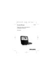
DVD Portable Player
PET716
All version
Service Manual
TABLE OF CONTENTS
Chapter
Technical Specification & Service Tips…………..……….. 1
Safety Instructions…………………………………………….. 2
Instruction for Use……………………………………………… 3
Mechanical Instructions………………………………………. 4
Troubleshooting …………………………………………………5
Overall Block Diagram…………………………………………. 6
Electrical Diagram……………………………………………… 7
Service Part List………………………………...………………. 8
Revision List……………………………………………………. 9
©Copyright 2005 Philips Consumer Electronics B.V. Eindhoven, The Netherlands
All rights reserved. No part of this publication may by reproduced, stored in a
retrieval system or transmitted, in any form or by any means, electronics,
mechanical, photocopying, or otherwise without the prior permission of Philips
3141 785 31862
Version 1.2
1.0 TECHNICAL SPECIFICATION
General
Dimensions (W x H x D):
Bear Unit Weight:
Power supply:
Power consumption:
Operating temp. & RH:
Video System
Audio System
Output voltage 1kHz:
THD 20-20kHz (%):
Dynamic range:
Signal/Noise ratio:
Frequency response (2020kHz):
Channel Separation 1kHz
Channel Balance 1kHz
210 x 178 x 39mm
719.3g +/- 5%
Input: 100-240V AC, 50/60Hz
0.3A
Output: DC 9V 1.0A
9W
-10 ~ +50degC / 40-90%
NTSC / PAL / AUTO
2+/-0.2V
</=3%
>/=70dB
>/=70dB
+/-1dB
>=60dB
<2dB
Current consumption
DVD, Picture-CD,
SVCD, Video CD, MP3CD, CD-R/CD-RW,
WMA-CD, DVD-R, DVDRW, DVD+R, DVD+RW
Video Playback Format:
DVD / VCD / JPEG
Audio Playback Format:
CD/MP3, MP3-DVD,
WMA
Disc Diameter
12cm
Pixel specification
Max. 0 bright-dot & max. 3 dark-dots
Factory Service Mode (FSM)
DC-IN SUPPLY (9V)
Battery Charging Current
450 +/- 50mA
BATT. SUPPLY
Power Off
Playback with TFT on
Playback without TFT on
Playback time
Headphone out (headphone output load 2x16 ohm)
Maximum output power:
Frequency response:
SNR (A-wght):
THD (0.2-20kHz):
Left-Right Channel
Separation:
Left-Right Channel
Balance:
Playback disc type:
1.5mW
+/-1dB
>70dB
1%
>/=50dB
To check the software version and change
region code of your DVD Portable
1. Power ON the DVD player and open the DVD
door
2. Press the “SETUP” button on remote control,
then select the “Preference MENU”
3. Press the remote button in the sequence as
9 -> 6 -> 5 -> 3
4. The LCD display showed the existing region
(navigation up) or
code. Press
(navigation down) repeatedly to select the
number from 0 to 6.
5. Refer below table for your region code setting
</=1dB
Supported disc type
Select “0” setting = Region Free (confidential)
Video Playback
Formats:
Audio Playback
Formats:
1.0 TECHNICAL SPECIFICATION
Procedure on how to upgrade the software of
the DVD Portable
For the best performance of your DVD Portable.
Check www.philips.com/support for latest
software upgrades available.
A) By CD-ROM
1.
2.
3.
4.
5.
Download the “PHILIPS.BIN” file from the Philips
support site
Unzip the file and then burn it into a CD-ROM to
make a disc for upgrade
CD-ROM disc name must be “PHILIPS”
(otherwise it will not be recognized as a disc for
upgrade)
Power on the Portable DVD Player with AC/DC
adaptor
Play CD-ROM for firmware upgrade
Warning: Do not unplug the AC adaptor during
firmware upgrade to prevent flash corrupt of the
set!!
6.
7.
Once upgrade is completed, the player will restart
automatically and observed PHILIPS LOGO on the
screen.
Open the DVD door to remove the disc
2.0 SAFTETY INSTRUCTIONS
GB
NL
ESD
WARNING
Alle IC’s en vele andere halfgeleiders zijn
gevoelig voor electrostatische ontladingen
(ESD).
Onzorgvuldig behandelen tijdens reparatie kan
de levensduur drastisch doen verminderen.
Zorg ervoor dat u tijdens reparatie via een
polsband met weerstand verbonden bent met
hetzelfde potentiaal als de massa van het
apparaat.
Houd componenten en hulpmiddelen ook op
ditzelfde potentiaal.
All ICs and many other semi-conductors are
susceptible to electrostatic discharges (ESD).
Careless handling during repair can reduce life
drastically.
When repairing, make sure that you are
connected with the same potential as the mass
of the set via a wrist wrap with resistance.
Keep components and tools also at this
potential.
F
WAARSCHUWING
ATTENTION
I
Tous les IC et beaucoup d’autres
semi-conducteurs sont sensibles aux
décharges statiques (ESD).
Leur longévité pourrait être considérablement
écourtée par le fait qu’aucune précaution n’est
prise à leur manipulation.
Lors de réparations, s’assurer de bien être relié
au même potentiel que la masse de l’appareil et
enfiler le bracelet serti d’une résistance de
sécurité.
Veiller à ce que les composants ainsi que les
outils que l’on utilise soient également à ce
potentiel.
D
AVVERTIMENTO
WARNUNG
Alle ICs und viele andere Halbleiter sind
empfindlich gegenüber elektrostatischen
Entladungen (ESD).
Unsorgfältige Behandlung im Reparaturfall kan
die Lebensdauer drastisch reduzieren.
Veranlassen Sie, dass Sie im Reparaturfall über
ein Pulsarmband mit Widerstand verbunden
sind mit dem gleichen Potential wie die Masse
des Gerätes.
Bauteile und Hilfsmittel auch auf dieses gleiche
Potential halten.
Tutti IC e parecchi semi-conduttori sono
sensibili alle scariche statiche (ESD).
La loro longevità potrebbe essere fortemente
ridatta in caso di non osservazione della più
grande cauzione alla loro manipolazione.
Durante le riparazioni occorre quindi essere
collegato allo stesso potenziale che quello della
massa dell’apparecchio tramite un braccialetto
a resistenza.
Assicurarsi che i componenti e anche gli utensili
con quali si lavora siano anche a questo
potenziale.
GB
Safety regulations require that the set be restored to its original
condition and that parts which are identical with those specified,
be used.
“Pour votre sécurité, ces documents
doivent être utilisés par des spécialistes agréés, seuls habilités à réparer
votre appareil en panne”.
NL
Veiligheidsbepalingen vereisen, dat het apparaat bij reparatie in
zijn oorspronkelijke toestand wordt teruggebracht en dat onderdelen,
identiek aan de gespecificeerde, worden toegepast.
CLASS 1
LASER PRODUCT
3122 110 03420
F
Les normes de sécurité exigent que l’appareil soit remis à l’état
d’origine et que soient utiliséés les piéces de rechange identiques
à celles spécifiées.
GB
Warning !
Invisible laser radiation when open.
Avoid direct exposure to beam.
D
Bei jeder Reparatur sind die geltenden Sicherheitsvorschriften zu
beachten. Der Original zustand des Geräts darf nicht verändert werden;
für Reparaturen sind Original-Ersatzteile zu verwenden.
S
Varning !
Osynlig laserstrålning när apparaten är öppnad och spärren
är urkopplad. Betrakta ej strålen.
SF Varoitus !
I
Le norme di sicurezza esigono che l’apparecchio venga rimesso
nelle condizioni originali e che siano utilizzati i pezzi di ricambio
identici a quelli specificati.
Avatussa laitteessa ja suojalukituksen ohitettaessa olet alttiina
näkymättömälle laserisäteilylle. Älä katso säteeseen!
DK Advarse !
"After servicing and before returning set to customer perform a
leakage current measurement test from all exposed metal parts to
earth ground to assure no shock hazard exist. The leakage current
must not exceed 0.5mA."
Usynlig laserstråling ved åbning når sikkerhedsafbrydere er
ude af funktion. Undgå udsaettelse for stråling.
2.1 ESD PROTECTION
Whenthepowersupplyisbeingturnedon,youmaynotremovethislasercautionslabel.Ifitremoves,radiationoflaser
maybereceived.
PREPARATIONOFSERVICING
PickupHeadconsistsofalaserdiodethatisverysusceptibletoexternalstaticelectrocity.
Althoughitoperatesproperlyafterreplacement,ifitwassubjecttoelectrostaticdischargeduringreplacement,
itslifemightbeshortened.Whenreplacing,useaconductivemat,solderingironwithgroundwire,etc.to
protectthelaserdiodeformdamagebystaticelectricity.
Andalso,theLSIandICaresameasabove.
Groundconductive
wriststrapforbody.
Solderingiron
withgroundwire
orceramictype
1M
Conductivemat
Thegroundresistance
betweenthegroundline
andthegroundislessthan10
SAFTY NOTICE
SAFTY PRECAUTIONS
LEAKAGE CURRENT CHECK
Plug the AC line cord directly into a 120V AC outlet (do
not use an isolation transformer for this check). Use an
AC voltmeter, having 5000 per volt or more sensitivity.
Connect a 1500 10W resistor,paralleled by a 0.15uF
150V AC capacitor between a knomn good earth ground
(water pipe, conduit, etc.) and all exposed metal parts of
cabinet (antennas, handle bracket, metal cabinet
screwheads, metal overlays, control shafts, etc.).
Measure the AC voltage across the 1500 resistor.
The test must be conducted with the AC switch on and
then repeated with the AC switch off. The AC voltage
indicated by the meter may not exceed 0.3V.A reading
exceeding 0.3V indicates that a dangerous potential
exists, the fault must be located and corrected.
Repeat the above test with the DVD VIDEO PLAYER
power plug reversed.
NEVER RETURN A DVD VIDEO PLAYER TO THE
CUSTOMER WITHOUT TAKING NECESSARY
CORRECTIVE ACTION.
READING SHOULD NOT EXCEED 0.3V
AC VOLTMETER
DVD VIDEO PLAYER
(5000 per volt
or more sensitivity)
1500
10W
AC OUTLET
Good earth ground
such as a water pipe,
conduit, etc.
0.15uF 150V AC
Test all exposed metal.
Voltmeter Hook-up for Leakage Current Check
The lightning flash with arrowhead symbol, within an
equilateral triangle, is intended to alert the user to the
presence of uninsulated "dangerous voltage" within the
product's enclosure that may be of sufficient magnitude to
constitute a risk of electric shock to persons.
The exclamation point within an equilateral triangle is
intended to alert the user to the presence of important
operating and maintenance (servicing) instructions in the
literature accompanying the appliance.
3.0 INSTRUCTION FOR USE
4.0 MECHANICAL INSTRUCTION
Disassembly Procedure
1. Remove 7pcs of screws on the side of bottom cabinet.
2. Open the bottom cabinet, up-plug all the wire connecter
from main board (The wire connecter are for : DVD
loder, battery board and TFT driver board, Key board
and speaker) Remove all the screws on the main board,
then take the main board from bottom cabinet.
3. up-plug the FFC from DVD driver, then you can take out
the DVD Driver.
4. Remove the flex cable on the bottom side.
5. Remove 2 pcs of screws on the battery board. Then take
out the battery together with the battery board.
6. Remove 4pcs of screws on the display frame. Carefully
open the display frame with the catches by screwdriver.
(There are six catches as shown in the pictures) Refer to
next picture.
4.0 MECHANICAL INSTRUCTION
7. To remove the hinge, remove the screws on the hinge.
8. To remove the TFT, de-soldering the wire connected between
TFT and TFT board first. (Please note the wire location as
shown in picture during re-assembly) And up pulg wire
connecter from TFT board.
9. Take out the driver board from cabinet using eradicator.
5.0 TROUBLESHOOTING
SYMPTOM: BATTERY NO POWER
BATTERY CAN'T
Power ON
Start
Check Battery capacity?
no
Check charging
function OK?
Check adaptor
power-ON OK?
Yes
yes
SET OK?
Yes
No
Check the Power-ON
button and cable OK?
NO
Replace Button or
Cable
No
Yes
Replace Main Board
No Defect, return
set to Customer
5.0 TROUBLESHOOTING
SYMPTOM: NO IMAGE / NO SOUND
SYMPTOM: NO IMAGE OUTPUT ( THE PANEL SHOW BLUE PICTURE)
Start
Check DVD Drive work?
no
Replace DVD Drive
no
Exchange AV cable
yes
NOTE: AV Cable TYPE from outside to
Inside L-Audio, R-Audio, Video, Ground
Check the external AV
Cable TYPEnote and
connection is OK?
yes
Replace Main Board
SYMPTOM: NO SOUND COMES FROM SPEAKER
Start
Check the Connection OK?
no
Reinsertion
no
Change the speaker
yes
Check speaker OK?
yes
Replace Main Board
5.0 TROUBLESHOOTING
SYMPTOM: THE DVD DRIVE DOES NOT WORK
SYMPTOM: THE DVD DRIVE DOESN'T WORK
Start
Check DVD-Loader
connection OK?
NO
Cable Reinsertion
NO
Replace DVDLoader
Yes
Check the DVD-Loader
OK?
Yes
Replace main board
5.0 TROUBLESHOOTING
SYMPTOM: ADAPTOR CANNOT POWER ON
Adaptor can not Power ON
Start
Check Adaptor OK?
NO
Change adaptor
SET OK?
Yes
Yes
No
Check the Power-ON
button and cable OK?
YES
Return set to
Customer
Replace Main Board
NO
Replace Button or
Cable
OK
5.0 TROUBLESHOOTING
SYMPTOM: REMOTE CONTROL CANNOT WORK
SYMPTOM: THE REMOTE CONTROL CAN NOT
WORK
Start
Check CABLE form
bottom board to top board
connection OK?
NO
Cable Reinsertion
NO
Replace IR receiver
Yes
Check TOP-board OK?
NO
Replace top board
OK
Yes
OK
Replace main board
OK
Return to custormer
5.0 TROUBLESHOOTING
SYMPTOM: NO SOUND FROM HEADPHONE
5.0 TROUBLESHOOTING
SYMPTOM: LED DISPLAY FAILURE
SYMPTOM: LED Display Fail
Start
Check CABLE form Main board to top board
connection OK?
NO
Cable Reinsertion
Yes
Check TOP-board OK?
NO
Replace LED
NO
Replace top board
OK
Yes
OK
Replace main board
OK
Return to custormer
5.0 TROUBLESHOOTING
SYMPTOM: KEY & BOTTON FAILURE
SYMPTOM: Key & Botton Fail
Start
Check CABLE form board to
board connection OK?
NO
Cable Reinsertion
Yes
Check KEY board OK?
NO
OK
Yes
Replace main board
Replace KEY board
OK
Return to custormer
6.0 BLOCK DIAGRAM
7.0 Electrical Diagram
VCC1
2
3
VCC1
R222
33K
R224
39K
R226
10K
COLOR
R228
18K
PEAK-LIMIT
1
4
5
6
7
R234
56K
RGB-AMP
R236
56K
SUBB
C221
104
R227
5K1
SUBR
56K
C220
104
R225
R223
10K
C222
104
R229
12K
9
10
12
11
VCC
R232
OPEN
R230
OPEN
R240
39K
GM1
GM2
R242
18K
BRIGHT
VDD
CONTRAST
R3
100K
PICTURE
R305
15K
TIN
C219
104
8
R231
OPEN
C223
104
C228
104
C225
104
R235
22K
R233
OPEN
C224
104
C226
104
R241
18K
C227
104
R237
18K
C229
104
BOUT
R306 10K
C230
104
R243
OPEN
R6
100K
R8
100K
GOUT
ROUT
R7
100K
R1
00K
R9
100K
U301
IMT1
D
CSY
E1
R302
10K
R301
10K
B1
CSY
R303
100K
HSY
FRP
C2
D
3
4
2
5
1
6
C1
B2
E2
IC401
C301
150P
C302
390P
BLK
C3
100P
22uF/10V
C212
5
4
6
3
7
2
RB42 100
VCC
R304
39K
R307
39
R217
C303
OPEN
RT2
10
RT3
A
8
430
1
RT1
PLOS
47K
VDD
VRB4
50K
C1
4.7uF/25V
VCC
25
INH
39R
R160
R159
PDA
39R
R161
0
OPEN
R162
R20
100
100
OPEN
R163
49
50
52
51
53
54
55
56
57
59
58
60
61
63
OCPH1
OCPH2
OCPH3
OSTH1
OSTH2
OO2H
LCDD
OCPO
OOEH
VSS
ICP1
IO2H-SEL
ITEST
VGL
VGH
OSCI
42
R144
41
R143
39
40
R142
39
VDD
BOUT
GOUT
ROUT
39
CLK
R21
0
STV
R4
R/L
INH
CLI1
38
R154 39R
37
36
STHL
10
R139
OPEN
35
R138
NC
34
R137
OPEN
R12
OE
STHL
39
VGL
COM
C
7" LG PANEL
33
32
31
561
561
R130
IRES2
IRESS
LVDD
C114
103
OSCO
39
IRES1
R131
17
MVCD
30
VDDH
C102
103
ITST1
HOVSY
IODO-SEL
16
VDDH
HONSY
ICPH-SEL
15
DOE3
29
14
OPEN
DOE2
ONPO
28
39R
R114
DOE1
CBL
OPEN
R18
CPOLC
OPEN
13
R129
12
0
R128
39R
R112
VSS
ICPO-SEL
11
R111
OSTV2
OPCLS
IMODE
R110
CPSC
27
10
39R
OPEN
VSYOUT
39R
OCPV
OSTV1
R127
OE
R109
IAREA-SEL
FRP
BLK
9
IHOS2
PLOS
39R
OPSI
STV
CLK
OE
43
HVDO
IC101
PVI-1004
CMCL
26
PSC
R108
CLOC
25
R245
8.2K
8
OPEN
R244
22K
39R
OPEN
7
R107
R126
OPEN
R125
R106
HSY
IHPOS1
39
CLK
VSS
R16
C231
104
45
44
IOSCO
24
C204
C205
104
COUPS
U/D
VDDH
46
VSS
23
5
1
2
3
4
5
6
7
8
9
10
11
12
13
14
15
16
17
18
19
20
21
22
23
24
25
26
27
28
29
30
0R
47
DOSCO
22
39R
CSY
OPEN
R104
48
DPDA
FRST
OPEN
12
11
10
473 9
OPEN
AY
R124
4
VDD
RA6
DSRST
R123
3
IVPOS2
10K
21
R102
VDDH
VSYNC
39R
VSY-IN
2
R122
OPEN
6
PEAK-LIMIT
R/L
U/D
1
R103
IOEH-SCL
R206
8K2
IVPOS1
C206
103
C101
1uF
20
TIN
62
64
14
13
CON?
C111
104
IUNR
R208 220R
R207
5K6
INNP
15
C207
474
R105
R205
1M
CLI1
VDDL
RGB-AMP
L201
18UH
10M
680P
C232
22P
C203
R202
OPEN
COLOR
R204
R201 220
8
7
6
5
4
3
2
1
100R
105
C202
10uF/16V
R203
C201
R151
39
16
CSY
PICTURE
R164
105
17
39R
TINT
C208
18
IUND
VCC2
27
26
BLK
SUB B
SUB R
28
29
FRP
GN1
30
31
GN2
34
33
32
S/H-R
BRIGHT
35
S/H-B
SYN N
PICTURE
C218
105
VCD IN
R11
39R
R156
39R
ROUT
R121
R219
OPEN
C217
105
C
AGC D
105
IMODE3
48
APC FILTER
AGC FILTER
C251
R157
39R
105
IMODE2
47
COLOR
CLAMP
105
GOUT
C209
20
19
C250
IMODE1
330K
46
105
19
R218
682
VCD OUT
BOUT
C210
22
21
105
C249
24
23
18
680K
VCOM
X201
4.4336MHZ(P)
C216
R216
F ADJ
R-Y/B-Y PHASE
BRIGHT
GND
ACC FILTER
45
C234
0.1U
VEE
TRAP
C233
10uF/16V
44
R DC
VCC
RGB AMP
R215 18K
IC201
D3031
CONTRAST
PEAK LIMIT
L203
18uH
R IN
CILLER FILTER
43
RD
SW
42
G DC
G IN
CDLOR
41
CONTRAST
VDDH
GD
B IN
CIN
40
BO
B DC
SYN SEP
IDENT FILTER
VCC1
39
SYNC
S/H-G
36
38
VIDEO IN
37
H FILTER DUT
R214 1K
10K
RT6
A
VCC
10K
RT8
5.6K
CA6
0.01
STHL
104
C211
SUBR
SUBB
GM2
R212
100R
GM1
R213
000R
BRIGHT
R246 10K
R116
10K
L6
18uH
VDD
C103
104
L3
18uH
VDD1
OPEN
R132
561
CON?
VDDH
9V
CA8
1uF
CT2
0.1uF
+5V
DA1
DA204
LA1
VGH
18uH
LA5 22uH
Y
C
CA16
0.1uF
BR
CA14
10uF/16V
DA3
BAS85
RA1
100
RA5
OPEN
RA2
1M
CA15
1M
CA2
4.7uF/25V
5 3
4
2 1
CA10
1uF
ICP1
EL7630
CA18
OPEN
RA7
9K1
R/L
C103
103
B
R16
R14
CA11
1uF
CA5
4.7uF/25VV
560
CA21
0.1uF
1U
C9
CA4
4.7uF/25V
6800PF
R15
22K
CA3
0.1uF
CA9
0.1uF
C10
15K
PAD
CA12
1uF
7.5V
VCC
U/D
VGL
18uH
DA6
DA204
RA3
27K
DA4
DA204
LA2 18uH
1K
LA3
WIDE
CON7
1K
R135
VDDL
VGH
CA22
OPEN
CA1
4.7uF/25V
LA4 22uH
R136
OSCI
CA17
10uF/16V
WIDE
R120
VDDH
VDDH
1
2
3
4
5
6
7
101
OPEN
C104
104
Q10
SS9969
B
R118
R119
WIDE
C6
D1
56P
ISV215
C8
VR1
10K
10P
L1
6.8UH
MP1029_ACTION
MP1029_ACTION.SCH
C7
68P
150P
OSCO
IL
LV
IS
IS
LV
IL
DIM
DIM
C5
A
A
TITLE: PET76 MONITOR
APPROVED
1
2
3
4
5
6
7
8
9
10
11
CHECKED
DRAWER
REV:
0
GEYULAN
Date:
20070310
12
5
4
3
2
1
U5
B+
7.0 Electrical Diagram
CHECK
U6
B-
D
CHECK
F1
U1
D
B1184 Q3
B+
1
1.25A
C6
10UF
1
R33
1M
3
D10
1
C2
1
U2
1
U3
2
LED
R29
221
R32
10K
Q20
2412
IC1
7805
2
R22
150K
R19
10M
U4
Q5
2412
C7
R30
R17
3K3
IC11
Q4
C945
1UF
VDD
2
VSS
3
DO
CO
R137
470K
C83
0.1UF
C
0.47UF
4
R21
10M
B-
R135
1K
IC2
R9
100K
1
VSS VDD
8
2
XIN P0.0
7
XOUTP0.1
6
P1.2 P0.2
5
2
OPEN
LED
R11
470
3
4
R24
10K
R16
12K
1
R15
470
4
2
R3
R13
R14
C84
0.1UF
C10
104
0.1
47K
0.1
C85
0.1UF
0.1
R10
104
LM358
B
C1
D1
7
R4
+
5
-
IC3A
C9
104
6
+
3
LM358
S3C9444
R23
0R
Q7
2312
8
C12
10UF
R5
100K
C8
104
2
R1
1
C30
10UF
R12
10K
R20
3K3
1
C4
0.47UF
R18
2K2
1
30K
R31
47K
C5
R2
OPEN
C
B
S-8241ABJ
100K
5
R7
VM
1
GND
4
1
R6
221
2
3
SK34
2
1
R138
470K
Q6
SI2313
10UF\25v
BAS85
8
IC3B
R25
10K
1.8K
R27
1K
C3
0.1UF
R26
OPEN
A
A
.
TITLE:LMD-4808UC BATTERY BOARD
APPROVED
5
4
3
2
CHECKED
DRAWER
REV:
SHILIHUA
DATE:
1
0
2006-06-20
5
4
4
3
2
1
9V_IN
9V_IN
RESET Circuit
DC_IN
DC_IN
DV33
DC_IN
4
URST#
IR
2
2
D1
URST#
IR
D
VCC3
IR1
R1
1K
TP1
R2
10k
1N4148
15V
P+5V
1
2
3
2
GND
URST#
R3
2,3,4,5
GND
1K
R5
10
IR
Q1
3904
3
AVCC
GND
R4
10
IR_IN
D
1
AVCC
IR
POWER_SW
D2
2
VCC3
+
2
CE1
10uF/6.3v
GND
BC1
0.1UF
靠近主芯片
+ EC1
100uF/16V
GND
GND
D3
1
2
SS14
DC_IN
9V_IN
3
Q2
2307
R7
47K
C
R6
10K
BC2
NC
1
L1
SI2307
2
22UH
VCC3
Q3
VDD
1
U1
EXT
4
C
L2
FB / 0805
Q4
3904
EC2
100UF/16V
VOUT
GND
3
S8521F33MC
2
3
+
1
GND
1
R8
1K
EC7
100UF/16V
1
POWER_SW
VSS
2
ON/OFF
BC3
0.1UF
EC3
100UF/16V
2
9V_LCD
2
2
1
3
5
DC_IN
D4
9V_IN
Q5
SI2307
47K
R12
1
2
EC4
100uF/16V
2
J2
1K
GND
3
1
GND
+
Q8
NC
EXT
4
VOUT
3
L5
FB / 0805
1
2
1
1
Q9
100k
S8521F50MC
BC5
0.1UF
GND
EC6
100UF/16V
2,3,4,5
2
R15
1
R14
9V_IN
B
22UH
ON/OFF
EC5
100UF/16V
VSS
GND
U2
R13
100k
L4
VCC5
GND
3904
SI2307
3
2
DV33
DV33
Q6
1
OPEN/CLOSE_SW
LED3.0
2
DC_IN
SI2307
3
2
BC4
0.1uF
Q7
LED1
2
L9
10uH_0805
1
R10
47K
2
SS14
2
1
4
3
2
1
CHARGE
DISCHARGE
1LED
R11
SI2307
3
2
1
L3
3
VDD
4PIN/1.25mm(TO SPEAKER)
5
J1
D5
GND
B
SS14
R16
10k
2
BATTER
VCC3
VCC5
10k
L6
FB / 0805
L7
FB / 0805
1.8V POWER FOR DSP KERNEL
VCC3
1
1
3
R17
1.5K
2
4
2
POWER_SW
2
Batter
5
2
100uF/16V
GND
GND
GND
4
A
7.0 Electrical Diagram
6
J4
POWER LED
EC8
100uF/16V
0.1uF
GND
3
LED2
LED3.0
+
BC7
0.1UF
BC9
EC10
OFF
1
GND
47uF/16V
RFV33
AVCC
+
1
2
GND
A
BC8
OUT1
OUT2
0.1uF
1
VCC3
+
EC9
DC JACK(+9V~+12V)
IN
1
3
SS14
1
J3
L8
FB / 0805
V18
U3
APL1117-18V
DP1
2
DC_IN
2
2A_FUSE
2
ADJ
F1
1
DV33
P+5V
ON
POWER ON/OFF SWITCH
DESIGN
APPROVED
Title
POWER
Size
C
Date:
5
4
3
2
Document Number
Rev
B
PET716 DVD MAIN BOARD
2005.12.12
Sheet
1
1
of
4
5
4
3
2
1
V18
L11
RFVDD3
CE6
47uF/6.3v
0.1uF
C8
0.1uF
C13
10uF/10v
CE8
CE2
10uF/16v
CE4
+
1500pF
C60
10uF/10v
XI
0.1uF
XT1
XI
XO
XO
DACVDD3
YUV3
DACVDD3
YUV1
YUV2
APLLVDD3
AADVDD3
ADVCM
89_AR
89_AL
ADACVDD3
ADACVDD3
27MHz
RFV18
JITFN
JITFO
PLLVDD3
0.047uF
C17
RFVDD3
0.047uF
4.7uF
C9
0.1uF
TRIN
2
C23
1uF
C22
1
2
3
4
5
6
7
8
9
10
11
12
13
14
15
16
17
18
19
20
21
22
23
24
25
26
27
28
29
30
31
32
33
34
35
36
37
38
39
40
41
42
43
44
45
46
47
48
49
50
51
52
53
54
1uF
1uF
C
RFO
100
GND
1uF
C24
1uF
C25
C
D
A
B
C26
1uF
ADIN
OPO
E
F
OPOP+
R25
150k
R26
150k
MDI1
MDI2
R27
C29
2200pF
LDO2
LDO1
680k
V1P4
RFVDD3
CB12
1
DV33
R28
0.1uF
V2P8
V20
V1P4
10k
TEZISLV
SLSL+
OPO
OPOP+
DMO
FMO
C30
J7
0.1uF
J6
4x1 W/HOUSING
CON4
1
2
TRO
FOO
ADIN
2x1 W/HOUSING
CON2
IO_3
IO_6
STBY
Arima
OPA-601PH
AVCC
L17
GND
V20
AVCC1
E
F
D
A
B
C
RFO
GND
MDI1
GND
+
Pin Assignment v1.4
A18
A19
EC11
100uF/16v
DV33
162
161
160
159
158
157
156
155
154
153
152
151
150
149
148
147
146
145
144
143
142
141
140
139
138
137
136
135
134
133
132
131
130
129
128
127
126
125
124
123
122
121
120
119
118
117
116
115
114
113
112
111
110
109
DACVDD3
CB23
FB
0.1uF
Very Important to
reduce Noise
0.1uF
10uH
1
10
CB7
CB8
CB9
CB10
CB11
MA4
MA5
MA6
MA7
MA8
MA9
MA11
DCKE
0.1uF
0.1uF
0.1uF
0.1uF
0.1uF
DCLK
MA3
MA2
MA1
CB13
CB14
CB15
CB16
B
0.1uF
0.1uF
0.1uF
0.1uF
CB17
CB18
CB19
CB20
CB21
CB22
0.1uF
0.1uF
0.1uF
0.1uF
0.1uF
0.1uF
MA0
MA10
BA1
BA0
CS#
RAS#
CAS#
WE#
DQM1
DQ8
DQ9
4
1
1,4
1
1
C
DV33
89_AL
89_AR
DQ10
DQ11
DQ12
DQ13
DQ14
DQ15
DQ0
DQ1
DQ2
DQ3
DQ4
89_AL
89_AR
A[0..20]
AD[0..7]
PRD#
PWR#
PCE#
R31
R32
R33
R34
FOSO
TRSO
FMSO
DMSO
C32
C33
330pF 330pF
C34
C35
0.1uF
0.015uF
39k
39k
15k
10k
DCKE
CAS#
RAS#
WE#
CS#
FOO
TRO
FMO
DMO
3
3
3
3
3
FLASH
MA[0..11]
3
DQ[0..15] 3
BA[0..1]
3
DQM[0..1]
DCLK
U11
MT1389E
LQFP216/SMD
4
4
A[0..20]
AD[0..7]
PRD#
PWR#
PCE#
DQM[0..1]
DCLK
3
3
DCKE
CAS#
RAS#
WE#
CS#
SDRAM
SCL
SDA
3
3
3
3
3
SCL
SDA
MUTE_DAC
3
3
B
MUTE_DAC
4
AUDIO INTERFACE
E3
C
AVCC
DV33
LDO_DVD
B
AVCC2
RFV33
4.7
E
R91
0
RFV33
Q18
RN2
4.7K
4.7K
47uF/16v
R43
1
U5
TP2
MO_VCC
T+
A
15
16
SL+ 17
18
19
20
21
FMSO
TRSO
V1P4
STBY
VOTK+
VOTKVOLD+
VOLDPGND
VNFTK
PVCC2
30
G2
22
23
24
25
26
27
28
PREGND
VINLD
CTK2
CTK1
VINTK
BIAS
STBY
VOFC+
VOFCVOSL+
VOSLPGND
PVCC1
VCC
14
13
12
11
10
9
8
G1
29
VNFFC
VOSL
VINSLVINSL+
CF2
CF1
VINFC
7
6
5
4
3
2
1
RS-232
J8
IO_0
IO_1
IO_2
IO_3
IO_4
IO_5
IO_6
2SB1132/8550
Q11
F-
T-
4
3
2
1
2N3906
LDO_CD
1
2
3
4
5
6
7
F+
R42
1
DV33
RxD
TxD
CON4
4PIN/2.0
+ CE10
3
2
C
CB26
0.1uF
MO_VCC
1
2
3
4
CE9
47uF/16v
RN3
1
2
3
4
3
+
4.7
10uH
L19
FB
10K IOA
R9
1
CB32
4
AVCC
VCC
URST#
IR
MA[0..11]
DQ[0..15]
BA[0..1]
2SB1132
R39
20k
4
YUV3
DV33
V18
Q10
2SB1132/8550
1
R40
C36
150pF
YUV2
IIC
L20
Arima OPA-601PH
R45
4
V18
TRIN
LIMIT
8
7
6
5
R36
SL-
4
YUV1
10
HEADER 24 SMD0.5 TOP
TP3
AVCC
VCC
URST#
IR
C
L18
WIDE
INT/EXT
V1P4
AVCC2
MDI2
R41
1
INT/EXT
2
R35
LD-CD
LD-DVD
D
1,3,4,5
C18
L16
PWR#
A16
A15
1
2
3
4
5
6
7
8
9
10
11
12
13
14
15
16
17
18
19
20
21
22
23
24
2
TOP
B
C31
0.1uF
CB24
0.1uF
MT1389E
55
56
57
58
59
60
61
62
63
64
65
66
67
68
69
70
71
72
73
74
75
76
77
78
79
80
81
82
83
84
85
86
87
88
89
90
91
92
93
94
95
96
97
98
99
100
101
102
103
104
105
106
107
108
FB
HA1
YUV3
IOA18
IOA19
IOWR#
A16
HIGHA7
DVDD3
HIGHA6
HIGHA5
HIGHA4
HIGHA3
HIGHA2
HIGHA1
IOA20
IOCS#
IOA1
IOOE#
AD0
AD1
AD2
DVSS
AD3
AD4
AD5
AD6
IOA21
ALE
AD7
A17
IOA0
DVDD18
UWR#
URD#
DVDD3
UP1_2
UP1_3
GPIO6
UP1_4
UP1_5
UP1_6
UP1_7
UP3_0
UP3_1
UP3_4
UP3_5
GPIO7
ICE
PRST#
IR
INT0#
DQM0#
RD7
RD6
RD5
DVDD3
A2
V18
A3
A4
A5
A6
A7
A8
YUV2
FS
VREF
8
7
6
5
R29
4
3
2
1
C
SPSP+
LIMIT
GND
YUV1
DQM0
DQ7
DQ6
DQ5
680k
C28
0.1uF/N.C
URST#
IR
R24
27P
V18
FS
VREF
DACVDDC
SPDIF
MC_DATA
ASDATA3
ASDATA2
ASDATA1
ASDATA0
ALRCK
ACLK
ABCK
GPIO5
DVSS
GPIO4
GPIO3
DVDD18
RA4
RA5
RA6
RA7
RA8
RA9
RA11
CKE
DVDD3
RCLK
RA3
RA2
RA1
DVDD18
RA0
RA10
BA1
BA0
RCS#
RAS#
CAS#
RWE#
DQM1
RD8
RD9
DVSS
RD10
RD11
RD12
RD13
RD14
RD15
RD0
RD1
RD2
RD3
RD4
IO_2
IOA
IO_1
IO_0
SCL
SDA
WIDE
MUTE_DAC
RXD
TXD
2200pF
AD7
A17
A0
C27
AD3
AD4
AD5
AD6
IO_4
R182
AGND
DVDA
DVDB
DVDC
DVDD
DVDRFIP
DVDRFIN
MA
MB
MC
MD
SA
SB
SC
SD
CDFON
CDFOP
TNI
TPI
MDI1
MDI2
LDO2
LDO1
SVDD3
CSO/RFOP
RFLVL/RFON
SGND
V2REFO
V20
VREFO
FEO
TEO
TEZISLV
OP_OUT
OP_INN
OP_INP
DMO
FMO
TROPENPWM
PWMOUT1/ADIN0
TRO
FOO
FG/ADIN1
GPIO0/VSYNC#
GPIO1/HSYNC#
GPIO2
IOA2
DVDD18
IOA3
IOA4
IOA5
IOA6
IOA7
HIGHA0
A14
A13
A12
A11
A10
A9
IO_5
PCE#
A1
PRD#
AD0
AD1
AD2
OPEN/CLOSE_SW
C11
27P
GND
AVDD3
IREF
RFGC
OSN
OSP
RFGND
CRTPLP
HRFZC
RFRPAC
RFRPDC
RFVDD3
ADCVSS
ADCVDD3
LPFOP
LPFIN
LPFIP
LPFON
PLLVDD3
IDACEXLP
PLLVSS
JITFN
JITFO
XTALI
XTALO
RFVDD18
RFGND18
ADACVDD2
ADACVDD1
ALF(CTR)
ALS/SDATA0
AL/SDATA2
AVCM
AR/SDATA1
ARS
ARF(SW)
ADACVSS2
ADACVSS1
APLLVSS
APLLCAP
APLLVDD
AADVDD
AKIN1
ADVCM
AKIN2
AADVSS
R/Cr/CVBS/SY
B/Cb/SC
DACVSSA
G/Y/SY/CVBS
DACVDDA
DACVSSB
DACVDDB
CVBS
DACVSSC
1
C21
C10
WIDE
CE7
47uF/6.3v
10k
B
A
D
100K
+
R181
J5
R20
R23
0.1uF
C19
0.1uF
V1P4
CB6
+
CE3
220uF/10v
FB
680R
CE5
47uF/6.3v
0.033uF
R21
15k
C12
0.1uF
R19
V20
CB5
+
FB
FB
L15
0.1uF
C6
C14
C20
V2P8
CB4
DV33
CE4
100uF/6.3v
+
0.1uF
CB3
0.1uF
RFVDD3
CE13
47uF/6.3v
0.1uF
D
PLLVDD3
6.8
+
L12
L14
CB2
R22
AADVDD3
C61
10uH
DV33
ADACVDD3
APLLVDD3
DACVDD3
750k
2200pF
C15
L25
JITFN
390pF
216
215
214
213
212
211
210
209
208
207
206
205
204
203
202
201
200
199
198
197
196
195
194
193
192
191
190
189
188
187
186
185
184
183
182
181
180
179
178
177
176
175
174
173
172
171
170
169
168
167
166
165
164
163
DV33
C1
R18
C16
0.01uF
C7 1000pF
0.1uF
C4
STBY
TRIN
TCK
TMS
JITFO
100k
C3
RFVDD3
C2
FB
20PF
C5
RFV33
RFV33
0.1uF
0.1uF
RFV18
CB1
FB
+
V18
V1P4
L13
R44
1
SPSP+
MO_VCC
7.0 Electrical Diagram
A
R46
10k
R47
20k
DMSO
V1P4
R48
FOSO
reserve this circuit for
protection OPU
20k
C37
150pF
0.1uF
BA5954
R49
CB33
10k
0.1uF
+ CE11
DESIGN
47uF/16v
LDO2
LDO_DVD
LDO1
LDO_CD
APPROVED
Title
PORTABLE1389HD_FORYOU-DM520ANR
Size
Document Number
Custom
Rev
B
PET716 DVD MAIN BOARD
Date:
5
4
3
2
2005.12.12
Sheet
1
2
of
4
5
4
3
2
1
U6
2
2
2
2
2
2
2
2
2
2
D
DQ[0..15]
MA[0..11]
BA[0..1]
DQM[0..1]
DCLK
DCKE
CAS#
RAS#
WE#
CS#
DQ[0..15]
MA[0..11]
BA[0..1]
DQM[0..1]
DCLK
DCKE
CAS#
RAS#
WE#
CS#
SDRAM
2
2
2
2
2
PCE#
PRD#
PWR#
A[0..20]
AD[0..7]
PCE#
PRD#
PWR#
A[0..20]
AD[0..7]
FLASH
RN1
DRAS#
DCS#
DBA0
DBA1
C
4
3
2
1
MA0
MA1
MA2
MA3
MA4
MA5
MA6
MA7
MA8
MA9
MA10
MA11
DBA0
DBA1
23
24
25
26
29
30
31
32
33
34
22
35
20
21
A0
A1
A2
A3
A4
A5
A6
A7
A8
A9
A10/AP
A11
BA0/A13
BA1/A12
SDCLK
SDCKE
38
37
CLK
CKE
DCS#
DRAS#
DCAS#
DWE#
19
18
17
16
CS
RAS
CAS
WE
DQM0
DQM1
15
39
DQML
DQMH
36
40
NC
NC
54
41
28
VSS
VSS
VSS
RAS#
CS#
BA0
BA1
5
6
7
8
33
RA1
RA2
33
33
SDCKE
R51
33
DCKE
SDCLK
R52
33
DCLK
DCAS#
DWE#
CAS#
WE#
DQ0
DQ1
DQ2
DQ3
DQ4
DQ5
DQ6
DQ7
DQ8
DQ9
DQ10
DQ11
DQ12
DQ13
DQ14
DQ15
2
4
5
7
8
10
11
13
42
44
45
47
48
50
51
53
VCC
VCC
VCC
1
14
27
VCCQ
VCCQ
VCCQ
VCCQ
3
9
43
49
VSSQ
VSSQ
VSSQ
VSSQ
6
12
46
52
DQ7
DQ6
DQ5
DQ4
DQ3
DQ2
DQ1
DQ0
DQ8
DQ9
DQ10
DQ11
DQ12
DQ13
DQ14
DQ15
2
DQ[0..15]
DQ[0..15]
DRAM
2
AD[0..7]
AD[0..7]
D
FLASH
SD33
SD33
DV33
SD33
L21
FB
C
+
CE12
CB34
CB35
CB36
CB25
100uF/10v
0.1uF
0.1uF
0.1uF
0.1uF
ESMT M12L64164A-7T
TSOP54
U7
B
DV33
A1
A2
A3
A4
A5
A6
A7
A8
A9
A10
A11
A12
A13
A14
A15
A16
A17
A18
A19
R56
DV33
10k
PCE#
PRD#
PWR#
25
24
23
22
21
20
19
18
8
7
6
5
4
3
2
1
48
17
16
9
10
A0
A1
A2
A3
A4
A5
A6
A7
A8
A9
A10
A11
A12
A13
A14
A15
A16
A17
A18
A19
A20
26
28
11
CE
OE
WE
12
A
D0
D1
D2
D3
D4
D5
D6
D7
D8
D9
D10
D11
D12
D13
D14
D15
29
31
33
35
38
40
42
44
30
32
34
36
39
41
43
45
WP/ACC
14
BYTE
47
VCC
37
GND1
GND2
27
46
AD0
AD1
AD2
AD3
AD4
AD5
AD6
AD7
B
DV33
DV33
BC12
DV33
0.1uF
A0
U8
1
2
3
4
CB37
0.1uF
A0
A1
A2
GND
VCC
WP
SCL
SDA
8
7
6
5
R54
R30
4.7K
4.7K
GND
SCL
SDA
2
2
24C01/CAT24C021
GND
I2C ADDR = 0XA0
RESET
A
MX29LV160
TSOP 48 pin
GND
Title
1,2,4,5
SDRAM&FLASH
Size
B
4
3
Rev
7.0 Electrical Diagram
Date:
5
Document Number
2
B
PET716 DVD MAIN BOARD
2005.12.12
Sheet
1
3
of
4
5
R59
5.1k
R58 10K
10uF/10V
C41
2
3
R50 100K
C40
R60
10uF/10V 330R
U9A
1
NJM4558
A_MUTE
R62
2
YUV2
2
YUV3
C43
100uF/10V
1K
2000p
L
5.6K
GND
3
3904
1,2,3,5
D
A_VCC
VER
+
DV33
DV33
C42
1
SOP8
R63 10K
2
A_L_SPEAKER
Q12
2700p
D
R61
ML_OUT
2
C39
LMAIN1
WIDE
WIDE
GND
270p
A_VCC
9V_IN
VCC3
A_VCC
DC_IN
8
2
1
2
3
4
5
ML_OUT
CVBS R
C38
+
1
CVBS_1
MR_OUT
MUTE_DAC
INT/EXT
A_VCC
9V_IN
VCC3
A_VCC
DC_IN
1
1
1
AV_1
+
MUTE_DAC
INT/EXT
2
4
89_AL
89_AR
2
2
3
R57
24K
89_AL
89_AR
+
2
2
4
YUV1
YUV1
-
2
R64
10K
CB22
0.1uF
AUD_GND
YUV2
DV33
YUV3
9V_IN
9V_IN
R65
24K
89_AL
GND
R53
4.7K
LMAIN1
89_AR
SC
WIDE
C44
RMAIN1
1
2
3
4
5
6
7
8
9V_LCD
SY
GND
270p
6
5
C47
A_MUTE
2700p
R70
1K
C59
100uF/16V
+
CB38
0.1uF
MR_OUT
C48
1
SOP8
9V_IN
R69
R68 330R
A_R_SPEAKER
Q13
8
MUTE_Circuit
NJM4558
控制屏的16:9,4:3
J9
8PIN/1.25mm
3904
5.6K
2000p
3
R38 100K
C46
10uF/10V
U9B
7
2
VER
10uF/10V
+
R66 10K
+
C45
RMAIN1
R67
5.1k
4
2
+
INT/EXT
-
INT/EXT
A_VCC
R37 1R/0805
D6
1
1N4148
2
L22 1.8uH
2
R71
C
R72
1K
D7
YUV1
C49
C
R73
75
220uF/16V
3
680K
1
1N4148
C52
+
VJ1
C50
C51
100P
100P
A_L_SPEAKER
R_HP_IN
Q14
3906
1
L_HP_IN
A_R_SPEAKER
470
A_MUTE
2
R74
SY
+
AUD_GND
100uF/16V
1
2
3
4
5
VOLUME 10K
BC6
L23 1.8uH
SC
YUV2
R75
75
VCC3
1
2
3
4
5
C53
C54
100P
100P
0.1UF
R76
3
4.7k
R55
MUTE_DAC
Q15
3906
1
L24 1.8uH
CVBS_1
YUV3
R77
100K
2
10k
100P
100P
R78
75
OUT_R
R79
330 PHONE_R
OUT_L
R80
330 PHONE_L
R81
0_0805
SP_L
AUD_GND
OUT_L
SP_R
OUT_R
B
9V_IN
1
2
3
4
5
6
7
8
9
10
11
L1
L2
R1
R2
GND
SW1
C56
B
SW2
C55
J10
PHONE-JACK
R82
1R(0805)
EC13
1uF/50V
R83
+
EC12
100uF/16V
200K
+
R_HP_IN
2
1
C57
470
NC 330P
3904(NC)
EC14
220uF/16V
7
3
R84
AUD_GND
2
Q16
A_MUTE
BC13
0.1uF
U10
OUT_R
1
10K
8
+
R85
+
AUD_GND
EC15
100uF/16V
AUD_GND
C58
6
NC 330P
R86
OUT_L
3
+
5
EC18
1uF/50V
EC16
220uF/16V
10K
BC14
+
EC17
100uF/16V
2
R87
4
+
L_HP_IN
APA2822
0.1uF
Q17
A_MUTE
R88
1
AUD_GND
A
470
0.1uF
4.7R
AUD_GND
R89
4.7R
A
7.0 Electrical Diagram
3904(NC)
3
R90
BC15
200K
AUD_GND AUD_GND
AUD_GND
SP_R
4
3
2
1
AUD_GND
SP_L
Title
A/V IN/OUT
J11
4PIN/1.25mm(TO SPEAKER)
Size
C
Document Number
Rev
4
3
2
B
PET716 DVD MAIN BOARD
Date: 2005.12.12
5
Sheet
1
4
of
4
5
4
IO-2
IO-1
SW1
D
MENU
1
2
1
IO-0
SW2
2
3
RIGHT
1
SW3
D
LEFT
2
1
2
IO-6
UP
BAND
1
PLAY/PAUSE
2
DSC
1
K5
2
DOWN
MUTE
1
K6
2
IO-5
STOP
SOURCE
1
2
NEXT
AUTO PROG/RAD PROG
1
2
IO-4
PRE
SOURCE
1
2
C
WIDE
AUTO PROG/RAD PROG
1
2
C
IO-3
B
B
A
A
7.0 Electrical Diagram
Title
KEY
Size
C
Document Number
Rev
5
4
3
2
B
PET716 KEY BOARD
Date:
Sheet
1
4
of
4
8.0 SERVICE PART LIST
Electrical Part List:
CTN
PET716/05
PET716/12
PET716/58
PET716S/05
PET716/05
PET716/12
PET716/58
PET716S/05
PET716/05
PET716/12
PET716/58
PET716S/05
PET716/05
PET716/12
PET716/58
PET716S/05
Service 12NC
996510002358
996510009821
996510009821
996510004269
996510009822
996510009822
996510002371
996510009827
996510009827
996510002368
996510009826
996510009826
Service Description
MAIN PCBA ASSY PET716
(for S/N: GS1Axxxxxxxx / below
VN1Cxxxxxxxx)
MAIN PCBA ASSY PET716LP
(for S/N: GS2Bxxxxxxxx or above /
VN1Cxxxxxxxx or above)
Photo
Pos.
No.
100
MAIN PCBA ASSY PET716LP
KEY PCBA ASSY PET716
(for S/N: GS1Axxxxxxxx / below
VN1Cxxxxxxxx)
KEY PCBA ASSY PET716LP
(for S/N: GS2Bxxxxxxxx or above /
VN1Cxxxxxxxx or above)
110
KEY PCBA ASSY PET716LP
TFT DRIVER PCB ASSY PET716
(for S/N: GS1Axxxxxxxx / below
VN1Cxxxxxxxx)
TFT DRIVER PCB ASSY PET716LP
(for S/N: GS2Bxxxxxxxx or above /
VN1Cxxxxxxxx or above)
120
TFT DRIVER PCB ASSY PET716LP
BATTERY PCB ASSY PET716
(for S/N: GS1Axxxxxxxx / below
VN1Cxxxxxxxx)
BATTERY PCB ASSY PET716LP
(for S/N: GS2Bxxxxxxxx or above /
VN1Cxxxxxxxx or above)
BATTERY PCB ASSY PET716LP
130
8.0 SERVICE PART LIST
Mechanical Part List:
CTN
PET716/05
PET716/12
PET716/58
Service
12NC
996510002360
996510009823
Service Description
7'' LCD PANEL ASSY LG A2
(for S/N: GS1Axxxxxxxx / below
VN1Cxxxxxxxx)
7'' LCD PANEL ASSY LG E2
(for S/N: GS2Bxxxxxxxx or above /
VN1Cxxxxxxxx or above)
PET716S/05
996510009823
7'' LCD PANEL ASSY LG E2
PET716/05
PET716/12
PET716/58
996510002361
DVD LOADER PET716
PET716S/05
996510007686
DVD LOADER PET716S
PET716/05
PET716/12
PET716/58
PET716S/05
996510002384
FFC 24P
Photo
Pos.
No.
200
210
220
8.0 SERVICE PART LIST
Mechanical Part List:
No.
Service
12NC
PET716/05
PET716/12
PET716/58
996510004270
PET716S/05
996510007687
PET716/05
PET716/12
PET716/58
Service Description
Photo
Pos.
No.
FRONT CABINET PET716
300
996510004271
996510009824
FRONT CABINET PET716S
BOTTOM CABINET PET716
(for S/N: GS1Axxxxxxxx / below
VN1Cxxxxxxxx)
BOTTOM CABINET PET716LP
(for S/N: GS2Bxxxxxxxx or above /
VN1Cxxxxxxxx or above)
PET716S/05
996510009923
BOTTOM CABINET PET716S
PET716/05
PET716/12
PET716/58
996510004279
DISPLAY FRAME & SPEAKER
PET716
PET716S/05
996510009928
DISPLAY FRAME & SPEAKER
PET716S
PET716/05
PET716/12
PET716/58
996510004277
DVD TOP CABINET PET716
PET716S/05
996510009922
DVD TOP CABINET PET716S
PET716/05
PET716/12
PET716/58
996510004278
CD DOOR PET716
PET716S/05
996510009924
CD/DVD DOOR PET716S
PET716/05
PET716/12
PET716/58
996510004276
LENS PET716
PET716S/05
996510007690
LENS PET716S
PET716/05
PET716/12
PET716/58
PET716S/05
996510002356
HINGE PET716
310
320
330
340
350
360
8.0 SERVICE PART LIST
Mechanical Part List:
CTN
Service
12NC
PET716S/05
996510009925
PLAY BUTTON PET716S
400
PET716/05
PET716/12
PET716/58
996510004272
NAVIGATION BUTTON PET716
400
PET716S/05
996510009927
NAVIGATION BUTTON PET716S
420
PET716/05
PET716/12
PET716/58
996510004273
OK BUTTON PET716
PET716S/05
996510009926
OK BUTTON PET716S
996510004274
KEY ASSY PET716
(for S/N: GS1Axxxxxxxx / below
VN1Cxxxxxxxx)
996510009825
KEY ASSY PET716LP
(for S/N: GS2Bxxxxxxxx or above /
VN1Cxxxxxxxx or above)
PET716/05
PET716/12
PET716/58
996510004275
OPEN BUTTON PET716
PET716S/05
996510007682
OPEN BUTTON PET716S
PET716/05
PET716/12
PET716/58
PET716S/05
996510002366
OPEN SPRING
440
PET716/05
PET716/12
PET716/58
996510004268
POWER BUTTON PET716
450
PET716/05
PET716/12
PET716/58
Service Description
Photo
Pos.
No.
410
420
430
8.0 SERVICE PART LIST
Accessories Part List:
Service 12NC
Service Description
996510002353
AC/DC ADAPTER EU (for
PET716/12, PET716/58)
996510005927
AC/DC ADAPTER UK (for
PET716/05)
996510009921
AC/DC ADAPTER UK (for
PET716S/05)
996510004265 /
996510004975
AV CABLE PET716 / for PET716S
996510004266 /
996510009920
CAR ADAPTOR PET716 / for
PET716S
996510004267 /
996510004972
REMOTE CONTROL PET716 / for
PET716S
Photo
Pos. No.
ACADAPTOR
AVCABLE
CARADAPTOR
RC
9.0 REVISION LIST
Version 1.0 (3141 785 31860)
• Initial release PET716/12
Version 1.1 (3141 785 31861)
• Update partlist for PET716/05 & PET716/58
Version 1.2 (3141 785 31862)
• Update partlist for PET716S/05