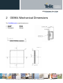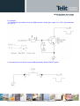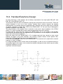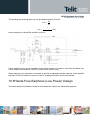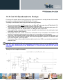
1
GE864 Hardware User Guide
1vv0300694 Rev.9 - 21/06/07
GE864 Hardware User Guide
1vv0300694 Rev.9 - 21/06/ 07
This document is relating to the following products:
GE864-QUAD 3990250648
GE864- PY
3990250650
Reproduction forbidden without Telit Communications S.p.A. written authorization - All Rights Reserved
page 2 of 79
GE864 Hardware User Guide
1vv0300694 Rev.9 - 21/06/ 07
Contents
1
Overview.......................................................................................................................................... 7
2
GE864 Mechanical Dimensions ................................................................................................ 8
3
GE864 module connections....................................................................................................... 9
3.1
3.1.1
4
BGA Balls Layout ................................................................................................................. 13
Hardware Commands................................................................................................................15
4.1
Turning ON the GE864-QUAD / PY........................................................................................15
4.2
Turning OFF the GE864-QUAD / PY......................................................................................17
4.2.1
4.2.2
5
PIN-OUT......................................................................................................................................9
Hardware shutdown .............................................................................................................. 17
Hardware Unconditional Restart ............................................................................................ 17
Power Supply...............................................................................................................................19
5.1
Power Supply Requirements.................................................................................................19
5.2
General Design Rules.............................................................................................................20
5.2.1
Electrical Design Guidelines .................................................................................................. 20
5.2.1.1 + 5V input Source Power Supply Design Guidelines ............................................................ 20
5.2.1.2 + 12V input Source Power Supply Design Guidelines .......................................................... 21
5.2.1.3 Battery Source Power Supply Design Guidelines ................................................................ 23
5.2.1.4 Battery Charge control Circuitry Design Guidelines ............................................................. 23
5.2.2
Thermal Design Guidelines ................................................................................................... 25
5.2.3
Power Supply PCB layout Guidelines ..................................................................................... 26
6
7
Antenna .........................................................................................................................................27
6.1
GSM Antenna Requirements .................................................................................................27
6.2
GSM Antenna - PCB line Guidelines.....................................................................................28
6.3
GSM Antenna - Installation Guidelines ................................................................................29
Logic level specifications .........................................................................................................30
7.1
8
9
Reset signal .............................................................................................................................31
Serial Ports ...................................................................................................................................32
8.1
MODEM SERIAL PORT ...........................................................................................................32
8.2
RS232 level translation...........................................................................................................34
8.3
5V UART level translation ......................................................................................................36
Audio Section Overview............................................................................................................38
9.1
Microphone Paths Characteristic and Requirements.........................................................39
9.2
General Design Rules.............................................................................................................42
Reproduction forbidden without Telit Communications S.p.A. written authorization - All Rights Reserved
page 3 of 79
GE864 Hardware User Guide
1vv0300694 Rev.9 - 21/06/ 07
9.3
Other considerations..............................................................................................................42
9.4
Microphone Biasing................................................................................................................43
9.4.1
9.4.2
9.5
Balanced Microphone Biasing................................................................................................ 43
Unbalanced Microphone Biasing............................................................................................ 44
Microphone Buffering.............................................................................................................46
9.5.1
9.5.2
Buffered Balanced Mic .......................................................................................................... 46
Buffered Unbalanced (Single Ended) Microphone . ................................................................. 48
10 OUTPUT LINES (Speaker).........................................................................................................51
10.1
Short description.................................................................................................................51
10.2
Output Lines Characteristics .............................................................................................52
10.3
General Design Rules .........................................................................................................53
10.3.1
Noise Filtering ...................................................................................................................... 53
10.4
Handset Earphone Design..................................................................................................54
10.5
Hands-Free Earphone (Low Power) Design.....................................................................55
10.6
Car Kit Speakerphone Design............................................................................................56
10.7
The Evaluation Kit for Telit Modules EVK2 ......................................................................57
10.7.1
10.7.2
Short Description .................................................................................................................. 57
EVK2 Audio Lines Characteristics.......................................................................................... 58
11 General Purpose I/O...................................................................................................................59
11.1
GPIO Logic levels................................................................................................................61
11.2
Using a GPIO Pad as INPUT ...............................................................................................62
11.3
Using a GPIO Pad as OUTPUT...........................................................................................62
11.4
Using the RF Transmission Control GPIO4......................................................................62
11.5
Using the RFTXMON Output GPIO5 ..................................................................................62
11.6
Using the Alarm Output GPIO6..........................................................................................63
11.7
Using the Buzzer Output GPIO7 ........................................................................................63
11.8
Indication of network service availability.........................................................................64
11.9
RTC Bypass out ...................................................................................................................65
11.10
VAUX1 power output...........................................................................................................65
12 DAC and ADC section................................................................................................................66
12.1
12.1.1
12.1.2
12.1.3
12.2
12.2.1
12.2.2
DAC Converter.....................................................................................................................66
Description ........................................................................................................................... 66
Enabling DA C....................................................................................................................... 67
Low Pass Filter Example ....................................................................................................... 67
ADC Converter.....................................................................................................................68
Description ........................................................................................................................... 68
Using ADC Converter............................................................................................................ 68
Reproduction forbidden without Telit Communications S.p.A. written authorization - All Rights Reserved
page 4 of 79
GE864 Hardware User Guide
1vv0300694 Rev.9 - 21/06/ 07
12.3
12.3.1
12.3.2
12.3.3
12.3.4
12.3.5
12.3.6
12.3.7
12.3.8
12.4
12.4.1
12.4.2
Mounting the GE864 on your Board..................................................................................69
General ................................................................................................................................ 69
Module finishing & dimensions............................................................................................... 69
Recommended foot print for the application (GE864) .............................................................. 70
Debug of the GE 864 in production ......................................................................................... 71
Stencil.................................................................................................................................. 71
PCB pad design.................................................................................................................... 72
Solder paste ......................................................................................................................... 73
GE864 Solder reflow ............................................................................................................. 74
Packing system....................................................................................................................75
GE864 orientation on the tray ................................................................................................ 76
Moisture sensibility ............................................................................................................... 76
13 Conformity Assessment Issues..............................................................................................77
14 SAFETY RECOMMANDATIONS ..............................................................................................78
15 Document Change Log..............................................................................................................79
Reproduction forbidden without Telit Communications S.p.A. written authorization - All Rights Reserved
page 5 of 79
GE864 Hardware User Guide
1vv0300694 Rev.9 - 21/06/ 07
DISCLAIMER
The information contained in this document is the proprietary information of Telit Communications
S.p.A. and its affiliates (“TELIT”). The contents are confidential and any disclosure to persons other
than the officers, employees, agents or subcontractors of the owner or licensee of this document,
without the prior written consent of Telit, is strictly prohibited.
Telit makes every effort to ensure the quality of the information it makes available. Notwithstanding the
foregoing, Telit does not make any warranty as to the information contained herein, and does not
accept any liability for any injury, loss or damage of any kind incurred by use of or reliance upon the
information.
Telit disclaims any and all responsibility for the application of the devices characterized in this
document, and notes that the application of the device must comply with the safety standards of the
applicable country, and where applicable, with the relevant wiring rules.
Telit reserves the right to make modifications, additions and deletions to this document due to
typographical errors, inaccurate information, or improvements to programs and/or equipment at any
time and without notice. Such changes will, nevertheless be incorporated into new editions of this
application note.
All rights reserved.
© 2006 - 2007 Telit Communications S.p.A.
Reproduction forbidden without Telit Communications S.p.A. written authorization - All Rights Reserved
page 6 of 79
GE864 Hardware User Guide
1vv0300694 Rev.9 - 21/06/ 07
1 Overview
The aim of this document is the description of some hardware solutions useful for developing a product with the
Telit GE864-QU AD / PY module.
In this document all the basic functions of a mobile phone will be taken into account; for each one of them a
proper hardware solution will be suggested and eventually the wrong solutions and common errors to be
avoided will be evidenced. Obviously this document cannot embrace the whole hardware solutions and products
that may be designed. The wrong solutions to be avoided shall be considered as mandatory, while the
suggested hardware configurations shall not be considered mandatory, instead the information given shall be
used as a guide and a starting point for properly developing your product with the Telit GE864-QU AD / PY module.
For further hardware details that may not be explained in this doc ument refer to the Telit GE864-QUA D / PY
Product Description document where all the hardware information is reported.
NOTICE
(EN) The integration of the GSM/GPRS GE864-QUAD / PY cellular module within user application shall be
done according to the design rules described in thi s manual.
(IT) L’integrazione del modulo cellulare GSM/GPRS GE864-QUAD / PY all’interno dell’applicazione
dell’utente dovrà ri spettare le indicazioni progettuali descritte in questo manuale.
(DE) Die integration des GE864-QUAD / PY GSM/GPRS Mobilfunk-Moduls in ein Gerät muß gemäß der in
diesem Dokument beschriebenen Kunstruktionsregeln erfolgen
(SL) Integracija GSM/GPRS GE864-QUAD / PY modula v uporabni ški aplikaciji bo morala upoštevati
projektna navodila, opi sana v tem piročniku.
(SP) La utilización del modulo GSM/GPRS GE864-QUAD / PY debe ser conform e a los usos para los cuales
ha sido deseñado descritos en este manual del usuario.
(FR) L’intégration du modul e cellulaire GSM/GPRS GE864-QUAD / PY dans l’application de l’utili sateur
sera faite selon les règles de conception décri tes dans ce manuel.
GE864-QUAD / PY
The information presented in this document is believed to be accurat e and reliable. However, no responsibility is
assumed by Telit Communications S.p.A. for its use, nor any inf ringement of patents or ot her rights of third
parties which may result from its use. No license is granted by implication or otherwise under any patent rights of
Telit Communications S.p.A. other than for circuitry embodied in Telit products. This document is subject to
change without notice.
Reproduction forbidden without Telit Communications S.p.A. written authorization - All Rights Reserved
page 7 of 79
GE864 Hardware User Guide
1vv0300694 Rev.9 - 21/06/ 07
2 GE864 Mechanical Dimensions
The Telit GE864 module overall dimension are:
•
•
•
Length:
Width:
Thickness:
30 mm
30 mm
2.8 mm
Reproduction forbidden without Telit Communications S.p.A. written authorization - All Rights Reserved
page 8 of 79
GE864 Hardware User Guide
1vv0300694 Rev.9 - 21/06/ 07
3 GE864 module connections
3.1 PIN-OUT
Ball
Signal
I/O
Function
Internal PULL UP
Type
Audio
H9
EAR_MT-
AO
Handset earphone signal output, phase -
Audio
G10
EAR_MT+
AO
Handset earphone signal output, phase +
Audio
H10
EAR_HF+
AO
Handsfree ear output, phase +
Audio
J10
EAR_HF-
AO
J9
MIC_HF-
AI
F9
AXE
I
Handsfree ear output, phase Handset mic.signal input; phase+, nom.
50mVrms
Handset mic.signal input; phase-, nom.
50mVrms
Handsfree mic. input; phase +, nom.
3mVrms
Handsfree mic.input; phase -, nom.
3mVrms
Handsfree sw itching
C10
SIMCLK
O
External SIM signal – Clock
1,8 / 3V
E9
SIMRST
O
External SIM signal – Reset
1,8 / 3V
D10
SIMIO
I/O
External SIM signal - Data I/O
C11
SIMIN
I
External SIM signal - Presence (active low)
D4 1
SIMVCC
-
External SIM signal – Power supply for the SIM
D11
TX_TRACE
O
TX Data for debug monitor
CMOS 2.8V
F10
RX_TRACE
I
RX Data for debug monitor
CMOS 2.8V
E7
C103/TXD
I
Serial data input (TXD) from DTE
CMOS 2.8V
H8
C104/RXD
O
CMOS 2.8V
B7
C108/DTR
I
F7
C105/RTS
I
F6
C106/CTS
O
D9
C109/DCD
O
E11
C107/DSR
O
Serial data output to DTE
Input for Data terminal ready signal (DTR) from
DTE
Input for Request to send signal (RTS) from
DTE
Output for Clear to send signal (CTS) to DTE
Output for Data carrier detect signal (DCD) to
DTE
Output for Data set ready signal (DSR) to DTE
B6
C125/RING
O
Output for Ring indicator signal (RI) to DTE
CMOS 2.8V
J8
MIC_MT+
AI
G9
MIC_MT-
AI
G8
MIC_HF+
AI
Audio
level
Audio
level
Audio
level
Audio
level
Audio
100K
CMOS 2.8V
SIM card interface
1,8 / 3V
47K
1,8 / 3V
1,8 / 3V
Trace
Prog. / Data + HW Flow Control
1
CMOS 2.8V
CMOS 2.8V
CMOS 2.8V
CMOS 2.8V
CMOS 2.8V
On this line a maximu m of 10nF bypass capacitor is allo wed
Reproduction forbidden without Telit Communications S.p.A. written authorization - All Rights Reserved
page 9 of 79
GE864 Hardware User Guide
1vv0300694 Rev.9 - 21/06/ 07
Ball
Signal
I/O
Function
Internal PULL UP
Type
DAC and ADC
C7
DAC_OUT
AO
Digital/Analog converter output
D/A
J11
ADC_IN1
AI
Analog/Digital converter input
A/D
H11
ADC_IN2
AI
Analog/Digital converter input
A/D
G11
ADC_IN3
AI
Analog/Digital converter input
A/D
Miscellaneous Functions
A2
RESET*
I
Reset input
E2
VRTC
AO
VRTC Backup capacitor
Pow er
D8
STAT_LED
O
Status indicator led
CMOS 1.8V
G1
CHARGE
AI
Charger input (*)
Pow er
G2
CHARGE
AI
Charger input (*)
Pow er
J5
ON_OFF*
I
D5
VAUX1
-
Input command for sw itching power ON or OFF
(toggle command). The pulse to be sent to the
47K
GE864 must be equal or greater than 1
second.
Pow er output for external accessories
L8
PWRMON
O
Pow er ON Monitor
L4
Antenna
O
Antenna output - 50 ohm
Pull up to VBATT
CMOS 2.8V
RF
GPIO
G4
TGPIO_12
I/O
Telit GPIO12 Configurable GPIO
CMOS 2.8V
C2
TGPIO_03
I/O
CMOS 2.8V
B3
TGPIO_04
I/O
C3
TGPIO_20
I/O
Telit GPIO03 Configurable GPIO
Telit GPIO04 Configurable GPIO / RF
Transmission Control
Telit GPIO20 Configurable GPIO
B4
TGPIO_14
I/O
Telit GPIO14 Configurable GPIO
CMOS 2.8V
D1
TGPIO_11
I/O
Telit GPIO11 Configurable GPIO
CMOS 2.8V
B1
TGPIO_19
I/O
Telit GPIO19 Configurable GPIO
CMOS 2.8V
C1
TGPIO_01
I/O
Telit GPIO01 Configurable GPIO
CMOS 2.8V
K7
TGPIO_18
I/O
Telit GPIO18 Configurable GPIO
CMOS 2.8V
H5
TGPIO_17
I/O
Telit GPIO17 Configurable GPIO
CMOS 2.8V
F5
TGPIO_15
I/O
Telit GPIO15 Configurable GPIO
CMOS 2.8V
K11
TGPIO_08
I/O
Telit GPIO08 Configurable GPIO
CMOS 2.8V
B5
TGPIO_06 / ALARM
I/O
Telit GPIO06 Configurable GPIO / ALARM
CMOS 2.8V
C9
TGPIO_09
I/O
Telit GPIO09 GPIO I/O pin
CMOS 2.8V
E6
TGPIO_02 / JDR
I/O
Telit GPIO02 I/O pin / Jammer detect report
CMOS 2.8V
L9
TGPIO_07 / BUZZER
I/O
Telit GPIO07 Configurable GPIO / Buzzer
CMOS 2.8V
H6
TGPIO_16
I/O
Telit GPIO16 Configurable GPIO
CMOS 2.8V
K10
TGPIO_13
I/O
CMOS 2.8V
K8
TGPIO_05 / RFTXMON I/O
L10
TGPIO_21
I/O
Telit GPIO13 Configurable GPIO
Telit GPIO05 Configurable GPIO / Transmitter
ON monitor
Telit GPIO21 Configurable GPIO
E8
TGPIO_22
I/O
Telit GPIO22 Configurable GPIO
H3
TGPIO_10
I/O
Telit GPIO10 Configurable GPIO
J1
VBATT
-
Main pow er supply
CMOS 2.8V
CMOS 2.8V
CMOS 2.8V
CMOS 2.8V
CMOS 1.8V
(not 2.8V !!)
CMOS 2.8V
Power Supply
Reproduction forbidden without Telit Communications S.p.A. written authorization - All Rights Reserved
Pow er
page 10 of 79
GE864 Hardware User Guide
1vv0300694 Rev.9 - 21/06/ 07
Ball
Signal
I/O
Function
Internal PULL UP
Type
K1
VBATT
-
Main pow er supply
Pow er
J2
VBATT
-
Main pow er supply
Pow er
K2
VBATT
-
Main pow er supply
Pow er
A1
GND
-
Ground
Pow er
F1
GND
-
Ground
Pow er
H1
GND
-
Ground
Pow er
L1
GND
-
Ground
Pow er
H2
GND
-
Ground
Pow er
L2
GND
-
Ground
Pow er
J3
GND
-
Ground
Pow er
K3
GND
-
Ground
Pow er
L3
GND
-
Ground
Pow er
K4
GND
-
Ground
Pow er
K5
GND
-
Ground
Pow er
D6
GND
-
Ground
Pow er
K6
GND
-
Ground
Pow er
L6
GND
-
Ground
Pow er
A11
GND
-
Ground
Pow er
F11
GND
-
Ground
Pow er
L11
GND
-
Ground
Pow er
RESERVED
A10
-
A3
-
A4
-
A5
-
A6
-
A7
-
A8
-
A9
-
B10
-
B11
-
B2
-
B8
-
B9
-
C4
-
C8
-
D2
-
D3
-
E1
-
E10
-
E3
-
E4
-
F2
-
Reproduction forbidden without Telit Communications S.p.A. written authorization - All Rights Reserved
page 11 of 79
GE864 Hardware User Guide
1vv0300694 Rev.9 - 21/06/ 07
Ball
Signal
I/O
F3
-
F4
-
G6
-
G7
-
H4
-
H7
-
J4
-
J6
-
J7
-
K9
-
L5
-
E5
-
L7
-
G5
-
G3
-
D7
-
C6
-
F8
-
C5
-
Function
Internal PULL UP
Type
NOTE: RESERVED pins must not be connected
NOTE: If not used, almost all pins should be left disconnected. The only exceptions are the following
pins:
pin
J1,K1,J2,K2
A1,F1,H1,L1,H2,L2,J3,K3,L3,
K4,K5,D6,K6,L6,A11,F11,L11
J5
E7
A2
H8
F7
1
signal
VBATT
GND
ON/OFF*
TXD
RESET*
RXD
RTS1
RTS should be connected to the GND ( on the module side) if flo w control is not used
Reproduction forbidden without Telit Communications S.p.A. written authorization - All Rights Reserved
page 12 of 79
GE864 Hardware User Guide
1vv0300694 Rev.9 - 21/06/ 07
3.1.1 BGA Balls Layout
TOP VIEW
A
B
C
D
E
F
G
H
J
K
L
1
GND
TGPIO_1 9
TGPIO_0 1
TGPIO_1 1
-
GND
CHARGE
GND
VBATT
VBATT
GND
2
RESET*
-
TGPIO_0 3
-
VRTC
-
CHARGE
GND
VBATT
VBATT
GND
3
-
TGPIO_0 4
TGPIO_2 0
-
-
-
VMICN
TGPIO_1 0
GND
GND
GND
4
--
TGPIO_1 4
-
SIMVCC
-
-
TGPIO_1 2
-
-
GND
Antenna
5
-
TGPIO_0 6
/ ALARM
VAUX1
-
TGPIO_1 5
VMICP
TGPIO_1 7
ON_OFF*
GND
-
6
-
C125/RING
GND
TGPIO_0 2
/ JDR
C106 /
CTS
-
TGPIO_1 6
-
GND
GND
7
-
C108 /
DTR
DAC_OUT
-
C103 /
TXD
C105 /
RTS
-
-
-
TGPIO_1 8
-
8
-
-
-
STAD_
LED
TGPIO_2 2
-
MIC_HF+
C104 /
RXD
MIC_MT+
TGPIO_0 5
/
RFTXMON
PWRMON
9
-
-
TGPIO_0 9
C109 /
DCD
SIMRST
AXE
MIC_MT-
EAR_MT-
MIC_HF-
-
TGPIO_0 7
/ BUZZER
10
-
-
SIMCLK
SIMIO
-
RX_TRACE
EAR_MT+
EAR_HF+
EAR_HF-
TGPIO_1 3
TGPIO_2 1
11
GND
-
SIMIN
TX_TRACE
C107 /
DSR
GND
ADC_IN3
ADC_IN2
ADC_IN1
TGPIO_0 8
GND
Reproduction forbidden without Telit Communications S.p.A. written authorization - All Rights Reserved
page 13 of 79
GE864 Hardware User Guide
1vv0300694 Rev.9 - 21/06/ 07
AUDIO Signals balls
SIM CARD interface balls
TRACE Signals balls
Prog. / data + Hw Flow Control signals balls
DAC and ADC signals balls
MISCELLANEOUS functions signals balls
TELIT GPIO balls
POWER SUPPLY VBATT balls
POWER SUPPLY GND balls
RESERVED
Reproduction forbidden without Telit Communications S.p.A. written authorization - All Rights Reserved
page 14 of 79
GE864 Hardware User Guide
1vv0300694 Rev.9 - 21/06/ 07
4 Hardware Commands
4.1 Turning ON the GE864-QUAD / PY
To turn on the GE864-QUAD / PY the pad ON# must be tied low for at least 1 seconds and then
released.
The maximum current that can be drained from the ON# pad is 0,1 mA.
A simple circuit to do it is:
ON#
R1
Q1
Power ON impulse
R2
GND
NOTE: don't use any pull up resistor on the ON# line, it is internally pulled up. Using pull up resistor may bring to
latch up problems on the GE864-QUAD / PY power regulator and improper power on/off of the module. The line ON#
must be connected only in open collector configuration.
NOTE: In this document all the lines that are inverted, hence have active low signals are labeled with a name that
ends with a "#" or with a bar over the name.
NOTE: The GE864-QUAD / PY turns fully on also by supplying power to the Charge pad (Module provided with a
battery on the VBATT pads).
TIP: To check if the device has powered on, the hardware line PWRMON should be monitored. After 900ms the line
raised up the device could be considered powered on.
PWRMON line rises up also when supplying power to the Charge pad
Reproduction forbidden without Telit Communications S.p.A. written authorization - All Rights Reserved
page 15 of 79
GE864 Hardware User Guide
1vv0300694 Rev.9 - 21/06/ 07
10k
For example:
1- Let's assume you need to drive the ON# pad with a totem pole output of a +3/5 V microcontroller
(uP_OUT1):
1s
2- Let's assume you need to drive the ON# pad directly with an ON/OFF button:
Reproduction forbidden without Telit Communications S.p.A. written authorization - All Rights Reserved
page 16 of 79
GE864 Hardware User Guide
1vv0300694 Rev.9 - 21/06/ 07
4.2 Turning OFF the GE864-QUAD / PY
The turning off of the device can be done in three ways:
• by software command (see GE864-QUAD / PY Software User Guide)
• by hardware shutdown
• by Hardware Unconditional Restart
When the device is shut down by software command or by hardware shutdown, it issues to the
network a detach request that informs the network that the device will not be reachable any more.
4.2.1 Hardware shutdown
To turn OFF the GE864-QUAD / PY the pad ON# must be tied low for at least 2 seconds and then
released.
The same circuitry and timing for the power on shall be used.
The device shuts down after the release of the ON# pad.
TIP: To check if the device has powered off, the hardware line PWRMON should be monitored. When PWRMON goes
low, the device has powered off.
4.2.2 Hardware Unconditional Restart
To unconditionally Restart the GE864-QUAD / PY, the pad RESET# must be tied low for at least 200
milliseconds and then released.
The maximum current that can be drained from the ON# pad is 0,15 mA.
A simple circuit to do it is:
RESET#
Unconditional Restart
impulse
GND
Reproduction forbidden without Telit Communications S.p.A. written authorization - All Rights Reserved
page 17 of 79
GE864 Hardware User Guide
1vv0300694 Rev.9 - 21/06/ 07
NOTE: don't use any pull up resistor on the RESET# line nor any totem pole digital output. Using pull up resistor
may bring to latch up problems on the GE864-QUAD / PY power regulator and improper functioning of the module.
The line RESET# must be connected only in open collector configuration.
TIP: The unconditional hardware Restart should be always implemented on the boards and software should use it
as an emergency exit procedure.
10k
For example:
1- Let's assume you need to drive the RESET# pad with a totem pole output of a +3/5 V
microcontroller (uP_OUT2):
Reset Signal Operating levels:
Signal
RESET Input high
RESET Input low
Min
2.2V*
0V
Max
3.3V
0.2V
* this signal is internally pulled up so the pin can be left floating if not used.
Reproduction forbidden without Telit Communications S.p.A. written authorization - All Rights Reserved
page 18 of 79
GE864 Hardware User Guide
1vv0300694 Rev.9 - 21/06/ 07
5 Power Supply
The power supply circuitry and board layout are a very important part in the full product design and
they strongly reflect on the product overall performances, hence read carefully the requirements and
the guidelines that will follow for a proper design.
5.1 Power Supply Requirements
The GE864-QUAD / PY power consumptions are:
GE864-QUAD/PY
Mode
Average (mA)
Mode description
IDLE mode
Stand by mode; no call in progress
AT+CFUN=1
23,9
Normal mode: full functionality of the module
AT+CFUN=4
22
AT+CFUN=0 or
AT+CFUN=5
7,20 / 3,56 1
Disabled TX and RX; module is not registered on the
network
Power saving: CFUN=0 module registered on the network
and can receive voice call or an SMS; but it is not possible
to send A T commands; module wakes up with an
unsolicited code (call or SMS) or rising RTS line. CFUN=5
full functionality with power saving; module registered on
the network can receive incoming calls and SMS
RX mode
1 slot in downlink
52,3
2 slot in downlink
65,2
3 slot in downlink
78,6
4 slot in downlink
88,4
GSM TX and RX mode
Min power level
78,1
Max power level
200,1
GPRS (class 10) TX and RX mode
Min power level
123,7
Max power level
370,8
GSM Receiving data mode
GSM Sending data mode
GPRS Sending data mode
The GSM system is made in a way that the RF transmission is not continuous, else it is packed into
bursts at a base frequency of about 216 Hz, the relative current peaks can be as high as about 2A.
Therefore the power supply has to be designed in order to withstand with these current peaks without
big voltage drops; this means that both the electrical design and the board layout must be designed for
this current flow.
1
Worst/best case depends on network configuration and is not under module control
Reproduction forbidden without Telit Communications S.p.A. written authorization - All Rights Reserved
page 19 of 79
GE864 Hardware User Guide
1vv0300694 Rev.9 - 21/06/ 07
If the layout of the PCB is not well designed a strong noise floor is generated on the ground and the
supply; this will reflect on all the audio paths producing an audible annoying noise at 216 Hz; if the
voltage drop during the peak current absorption is too much, then the device may even shutdown as a
consequence of the supply voltage drop.
TIP: The electrical design for the Power supply should be made ensuring it will be capable of a peak current output
of at least 2 A.
5.2 General Design Rules
The principal guidelines for the Power Supply Design embrace three different design steps:
• the electrical design
• the thermal design
• the PCB layout.
5.2.1 Electrical Design Guidelines
The electrical design of the power supply depends strongly from the power source where this power is
drained. We will distinguish them into three categories:
• +5V input (typically PC internal regulator output)
• +12V input (typically automotive)
• Battery
5.2.1.1 + 5V input Source Power Supply Design Guidelines
•
•
•
•
•
The desired output for the power supply is 3.8V, hence there's not a big difference between the
input source and the desired output and a linear regulator can be used. A switching power supply
will not be suited because of the low drop out requirements.
When using a linear regulator, a proper heat sink shall be provided in order to dissipate the power
generated.
A Bypass low ESR capacitor of adequate capacity must be provided in order to cut the current
absorption peaks close to the GE864-QUAD / PY, a 100µF tantalum capacitor is usually suited.
Make sure the low ESR capacitor on the power supply output (usually a tantalum one) is rated at
least 10V.
A protection diode should be inserted close to the power input, in order to save the GE864-QUAD /
PY from power polarity inversion.
Reproduction forbidden without Telit Communications S.p.A. written authorization - All Rights Reserved
page 20 of 79
GE864 Hardware User Guide
1vv0300694 Rev.9 - 21/06/ 07
An example of linear regulator with 5V input is:
5.2.1.2 + 12V input Source Power Supply Design Guidelines
•
•
•
•
•
•
•
•
The desired output for the power supply is 3.8V, hence due to the big difference between the input
source and the desired output, a linear regulator is not suited and shall not be used. A switching
power supply will be preferable because of its better efficiency especially with the 2A peak current
load represented by the GE864-QUAD/PY.
When using a switching regulator, a 500kHz or more switching frequency regulator is preferable
because of its smaller inductor size and its faster transient response. This allows the regulator to
respond quickly to the current peaks absorption.
In any case the frequency and Switching design selection is related to the application to be
developed due to the fact the switching frequency could also generate EMC interferences.
For car PB battery the input voltage can rise up to 15,8V and this should be kept in mind when
choosing components: all components in the power supply must withstand this voltage.
A Bypass low ESR capacitor of adequate capacity must be provided in order to cut the current
absorption peaks, a 100µF tantalum capacitor is usually suited.
Make sure the low ESR capacitor on the power supply output (usually a tantalum one) is rated at
least 10V.
For Car applications a spike protection diode should be inserted close to the power input, in order
to clean the supply from spikes.
A protection diode should be inserted close to the power input, in order to save the GE864QUAD/PY from power polarity inversion. This can be the same diode as for spike protection.
Reproduction forbidden without Telit Communications S.p.A. written authorization - All Rights Reserved
page 21 of 79
GE864 Hardware User Guide
1vv0300694 Rev.9 - 21/06/ 07
An example of switching regulator with 12V input is in the below schematic (it is split in 2 parts):
Reproduction forbidden without Telit Communications S.p.A. written authorization - All Rights Reserved
page 22 of 79
GE864 Hardware User Guide
1vv0300694 Rev.9 - 21/06/ 07
5.2.1.3 Battery Source Power Supply Design Guidelines
•
The desired nominal output for the power supply is 3.8V and the maximum voltage allowed is
4.2V, hence a single 3.7V Li-Ion cell battery type is suited for supplying the power to the Telit
GE864-QUAD/PY module.
The three cells Ni/Cd or Ni/MH 3,6 V Nom. battery types or 4V PB types MUST NOT BE USED
DIRECTLY since their maximum voltage can rise over the absolute maximum voltage for the
GE864-QUAD/PY and damage it.
NOTE: DON'T USE any Ni-Cd, Ni-MH, and Pb battery types directly connected with GE864-QUAD/PY. Their
use can lead to overvoltage on the GE864-QUAD/PY and damage it. USE ONLY Li-Ion battery types.
•
•
•
•
A Bypass low ESR capacitor of adequate capacity must be provided in order to cut the current
absorption peaks, a 100µF tantalum capacitor is usually suited.
Make sure the low ESR capacitor (usually a tantalum one) is rated at least 10V.
A protection diode should be inserted close to the power input, in order to save the GE864QUAD/PY from power polarity inversion. Otherwise the battery connector should be done in a way
to avoid polarity inversions when connecting the battery.
The battery capacity must be at least 500mAh in order to withstand the current peaks of 2A; the
suggested capacity is from 500mAh to 1000mAh.
5.2.1.4 Battery Charge control Circuitry Design Guidelines
The charging process for Li-Ion Batteries can be divided into 4 phases:
• Qualification and trickle charging
• Fast charge 1 - constant current
• Final charge - constant voltage or pulsed charging
• Maintenance charge
The qualification process consists in a battery voltage measure, indicating roughly its charge status. If
the battery is deeply discharged, that means its voltage is lower than the trickle charging threshold,
then the charge must start slowly possibly with a current limited pre-charging process where the
current is kept very low with respect to the fast charge value: the trickle charging.
During the trickle charging the voltage across the battery terminals rises; when it reaches the fast
charge threshold level the charging process goes into fast charge phase.
During the fast charge phase the process proceeds with a current limited charging; this current limit
depends on the required time for the complete charge and from the battery pack capacity. During this
phase the voltage across the battery terminals still raises but at a lower rate.
Once the battery voltage reaches its maximum voltage then the process goes into its third state: Final
charging. The voltage measure to change the process status into final charge is very important. It
must be ensured that the maximum battery voltage is never exceeded, otherwise the battery may be
damaged and even explode. Moreover for the constant voltage final chargers, the constant voltage
Reproduction forbidden without Telit Communications S.p.A. written authorization - All Rights Reserved
page 23 of 79
GE864 Hardware User Guide
1vv0300694 Rev.9 - 21/06/ 07
phase (final charge) must not start before the battery voltage has reached its maximum value,
otherwise the battery capacity will be highly reduced.
The final charge can be of two different types: constant voltage or pulsed. GE864-QUAD/PY uses
constant voltage.
The constant voltage charge proceeds with a fixed voltage regulator (very accurately set to the
maximum battery voltage) and hence the current will decrease while the battery is becoming charged.
When the charging current falls below a certain fraction of the fast charge current value, then the
battery is considered fully charged, the final charge stops and eventually starts the maintenance.
The pulsed charge process has no voltage regulation, instead the charge continues with pulses.
Usually the pulse charge works in the following manner: the charge is stopped for some time, let's say
few hundreds of ms, then the battery voltage will be measured and when it drops below its maximum
value a fixed time length charging pulse is issued. As the battery approaches its full charge the off
time will become longer, hence the duty-cycle of the pulses will decrease. The battery is considered
fully charged when the pulse duty-cycle is less than a threshold value, typically 10%, the pulse charge
stops and eventually the maintenance starts.
The last phase is not properly a charging phase, since the battery at this point is fully charged and the
process may stop after the final charge. The maintenance charge provides an additional charging
process to compensate for the charge leak typical of a Li-Ion battery. It is done by issuing pulses with
a fixed time length, again few hundreds of ms, and a duty-cycle around 5% or less.
This last phase is not implemented in the GE864-QUAD/PY internal charging algorithm, so that the
battery once charged is left discharging down to a certain threshold so that it is cycled from full charge
to slight discharge even if the battery charger is always inserted. This guarantees that anyway the
remaining charge in the battery is a good percentage and that the battery is not damaged by keeping it
always fully charged (Li-Ion rechargeable battery usually deteriorate when kept fully charged).
Last but not least, in some applications it is highly desired that the charging process restarts when the
battery is discharged and its voltage drops below a certain threshold, GE864-QUAD/PY internal
charger does it.
As you can see, the charging process is not a trivial task to be done; moreover all these operations
should start only if battery temperature is inside a charging range, usually 5°C - 45°C.
The GE864-QUAD/PY measures the temperature of its internal component, in order to satisfy this last
requirement, it's not exactly the same as the battery temperature but in common application the two
temperature should not differ too much and the charging temperature range should be guaranteed.
NOTE: For all the threshold voltages, inside the GE864-QUAD/PY all threshold are fixed in order to
maximize Li-Ion battery performances and do not need to be changed.
NOTE: In this application the battery charger input current must be limited to less than 400mA. This can
be done by using a current limited wall adapter as the power source.
NOTE: When starting the charger from Module powered off the startup will be in CFUN4; to activate the
normal mode a command AT+CFUN=1 has to be provided. This is also possible using the POWER ON.
There is also the possibility to activate the normal mode using the ON_OFF* signal.
In this case, when HW powering off the module with the same line (ON_OFF*) and having the charger still
connected, the module will go back to CFUN4.
Reproduction forbidden without Telit Communications S.p.A. written authorization - All Rights Reserved
page 24 of 79
GE864 Hardware User Guide
1vv0300694 Rev.9 - 21/06/ 07
5.2.2 Thermal Design Guidelines
The thermal design for the power supply heat sink should be done with the following specifications:
• Average current consumption during transmission @PWR level max:
500mA
• Average current consumption during transmission @ PWR level min:
100mA
• Average current during Power Saving (CFUN=5):
4mA
• Average current during idle (Power Saving disabled)
24mA
NOTE: The average consumption during transmissions depends on the power level at which the device is requested
to transmit by the network. The average current consumption hence varies significantly.
Considering the very low current during idle, especially if Power Saving function is enabled, it is
possible to consider from the thermal point of view that the device absorbs current significantly only
during calls.
If we assume that the device stays into transmission for short periods of time (let's say few minutes)
and then remains for a quite long time in idle (let's say one hour), then the power supply has always
the time to cool down between the calls and the heat sink could be smaller than the calculated one for
500mA maximum RMS current, or even could be the simple chip package (no heat sink).
Moreover in the average network conditions the device is requested to transmit at a lower power level
than the maximum and hence the current consumption will be less than the 500mA, being usually
around 150mA.
For these reasons the thermal design is rarely a concern and the simple ground plane where the
power supply chip is placed can be enough to ensure a good thermal condition and avoid overheating.
For the heat generated by the GE864-QUAD / PY, you can consider it to be during transmission 1W
max during CSD/VOICE calls and 2W max during class10 GPRS upload.
This generated heat will be mostly conducted to the ground plane under the GE864-QUAD / PY; you
must ensure that your application can dissipate it.
Reproduction forbidden without Telit Communications S.p.A. written authorization - All Rights Reserved
page 25 of 79
GE864 Hardware User Guide
1vv0300694 Rev.9 - 21/06/ 07
5.2.3 Power Supply PCB layout Guidelines
As seen on the electrical design guidelines the power supply shall have a low ESR capacitor on the
output to cut the current peaks and a protection diode on the input to protect the supply from spikes
and polarity inversion. The placement of these components is crucial for the correct working of the
circuitry. A misplaced component can be useless or can even decrease the power supply
performances.
•
•
•
•
•
•
•
•
The Bypass low ESR capacitor must be placed close to the Telit GE864-QUAD / PY power input
pads or in the case the power supply is a switching type it can be placed close to the inductor to
cut the ripple provided the PCB trace from the capacitor to the GE864-QUAD / PY is wide enough
to ensure a dropless connection even during the 2A current peaks.
The protection diode must be placed close to the input connector where the power source is
drained.
The PCB traces from the input connector to the power regulator IC must be wide enough to ensure
no voltage drops occur when the 2A current peaks are absorbed. Note that this is not made in
order to save power loss but especially to avoid the voltage drops on the power line at the current
peaks frequency of 216 Hz that will reflect on all the components connected to that supply,
introducing the noise floor at the burst base frequency. For this reason while a voltage drop of 300400 mV may be acceptable from the power loss point of view, the same voltage drop may not be
acceptable from the noise point of view. If your application doesn't have audio interface but only
uses the data feature of the Telit GE864-QUAD / PY, then this noise is not so disturbing and power
supply layout design can be more forgiving.
The PCB traces to the GE864-QUAD / PY and the Bypass capacitor must be wide enough to
ensure no significant voltage drops occur when the 2A current peaks are absorbed. This is for the
same reason as previous point. Try to keep this trace as short as possible.
The PCB traces connecting the Switching output to the inductor and the switching diode must be
kept as short as possible by placing the inductor and the diode very close to the power switching
IC (only for switching power supply). This is done in order to reduce the radiated field (noise) at the
switching frequency (100-500 kHz usually).
The use of a good common ground plane is suggested.
The placement of the power supply on the board should be done in such a way to guarantee that
the high current return paths in the ground plane are not overlapped to any noise sensitive circuitry
as the microphone amplifier/buffer or earphone amplifier.
The power supply input cables should be kept separate from noise sensitive lines such as
microphone/earphone cables.
Reproduction forbidden without Telit Communications S.p.A. written authorization - All Rights Reserved
page 26 of 79
GE864 Hardware User Guide
1vv0300694 Rev.9 - 21/06/ 07
6 Antenna
The antenna connection and board layout design are the most important part in the full product design
and they strongly reflect on the product overall performances, hence read carefully and follow the
requirements and the guidelines for a proper design.
6.1 GSM Antenna Requirements
As suggested on the Product Description the antenna and antenna line on PCB for a Telit GE864QUAD / PY device shall fulfill the following requirements:
ANTENNA REQUIREMENTS
Frequency range
Bandwidth
Gain
Impedance
Input power
VSWR absolute
max
VSWR
recommended
Depending by frequency band(s) provided by
the network operator, the customer shall use
the most suitable antenna for that/those
band(s)
70 MHz in GSM850, 80 MHz in GSM900,
170 MHz in DCS & 140 MHz PCS band
Gain < 3dBi
50 ohm
> 2 W peak power
<= 10:1
<= 2:1
When using the Telit GE864-QUAD / PY, since there's no antenna connector on the module, the
antenna must be connected to the GE864-QUAD / PY through the PCB with the antenna pad.
In the case that the antenna is not directly developed on the same PCB, hence directly connected at
the antenna pad of the GE864-QUAD / PY, then a PCB line is needed in order to connect with it or
with its connector.
Reproduction forbidden without Telit Communications S.p.A. written authorization - All Rights Reserved
page 27 of 79
GE864 Hardware User Guide
1vv0300694 Rev.9 - 21/06/ 07
This line of transmission shall fulfill the following requirements:
ANTENNA LINE ON PCB REQUIREMENTS
Impedance
50 ohm
Max Attenuation
0,3 dB
No coupling with other signals allowed
Cold End (Ground Plane) of antenna shall be equipotential to
the GE864-QUAD / PY ground pins
Furthermore if the device is developed for the US market and/or Canada market, it shall comply to the
FCC and/or IC approval requirements:
This device is to be used only for mobile and fixed application. The antenna(s) used for this transmitter
must be installed to provide a separation distance of at least 20 cm from all persons and must not be
co-located or operating in conjunction with any other antenna or transmitter. End-Users must be
provided with transmitter operation conditions for satisfying RF exposure compliance. OEM integrators
must ensure that the end user has no manual instructions to remove or install the GE864-QUAD / PY
module. Antennas used for this OEM module must not exceed 3dBi gain for mobile and fixed
operating configurations.
6.2 GSM Antenna - PCB line Guidelines
•
•
•
•
•
•
•
•
•
•
Ensure that the antenna line impedance is 50 ohm;
Keep the antenna line on the PCB as short as possible, since the antenna line loss shall be less
than 0,3 dB;
Antenna line must have uniform characteristics, constant cross section, avoid meanders and
abrupt curves;
Keep, if possible, one layer of the PCB used only for the Ground plane;
Surround (on the sides, over and under) the antenna line on PCB with Ground, avoid having other
signal tracks facing directly the antenna line track;
The ground around the antenna line on PCB has to be strictly connected to the Ground Plane by
placing vias once per 2mm at least;
Place EM noisy devices as far as possible from GE864-QUAD / PY antenna line;
Keep the antenna line far away from the GE864-QUAD / PY power supply lines;
If you have EM noisy devices around the PCB hosting the GE864-QUAD / PY, such as fast
switching ICs, take care of the shielding of the antenna line by burying it inside the layers of PCB
and surround it with Ground planes, or shield it with a metal frame cover.
If you don't have EM noisy devices around the PCB of GE864-QUAD / PY, by using a strip-line on
the superficial copper layer for the antenna line, the line attenuation will be lower than a buried
one;
Reproduction forbidden without Telit Communications S.p.A. written authorization - All Rights Reserved
page 28 of 79
GE864 Hardware User Guide
1vv0300694 Rev.9 - 21/06/ 07
6.3 GSM Antenna - Installation Guidelines
•
•
•
•
Install the antenna in a place covered by the GSM signal.
The Antenna must be installed to provide a separation distance of at least 20 cm from all persons
and must not be co-located or operating in conjunction with any other antenna or transmitter;
Antenna shall not be installed inside metal cases
Antenna shall be installed also according Antenna manufacturer instructions.
Reproduction forbidden without Telit Communications S.p.A. written authorization - All Rights Reserved
page 29 of 79
GE864 Hardware User Guide
1vv0300694 Rev.9 - 21/06/ 07
7 Logic level specifications
Where not specifically stated, all the interface circuits work at 2.8V CMOS logic levels. The following
table shows the logic level specifications used in the Telit GE864-QUAD / PY interface circuits:
Absolute Maximum Ratings -Not Functional
Parameter
Min
Max
Input level on any -0.3V
digital pin when on
Input voltage on -0.3V
analog pins when on
Voltage on Buffered -0.3V
pins
+3.6V
+3.0 V
25V
Operating Range - Interface levels (2.8V CMOS)
Level
Min
Max
Input high level
Input low level
Output high level
Output low level
2.1V
0V
2.2V
0V
3.3V
0.5V
3.0V
0.35V
For 2,0V signals:
Operating Range - Interface levels (2.0V CMOS)
Level
Min
Max
Input high level
Input low level
Output high level
Output low level
1.6V
0V
1,65V
0V
3.3V
0.4V
2.2V
0.35V
Current characteristics
Level
Typical
Output Current
Input Current
1mA
1uA
Reproduction forbidden without Telit Communications S.p.A. written authorization - All Rights Reserved
page 30 of 79
GE864 Hardware User Guide
1vv0300694 Rev.9 - 21/06/ 07
7.1 Reset signal
Signal
RESET
Function
Phone reset
I/O
I
Bga Ball
A2
RESET is used to reset the GE864-QUAD / PY modules. Whenever this signal is pulled low, the GE864QUAD / PY is reset. When the device is reset it stops any operation. After the release of the reset
GE864-QUAD / PY is unconditionally shut down, without doing any detach operation from the network
where it is registered. This behaviour is not a proper shut down because any GSM device is requested
to issue a detach request on turn off. For this reason the Reset signal must not be used to normally
shutting down the device, but only as an emergency exit in the rare case the device remains stuck
waiting for some network response.
The RESET is internally controlled on start-up to achieve always a proper power-on reset sequence,
so there's no need to control this pin on start-up. It may only be used to reset a device already on that
is not responding to any command.
NOTE: do not use this signal to power off the GE864-QUAD / PY. Use the ON/OFF signal to perform this
function or the AT#SHDN command.
Reset Signal Operating levels:
Signal
RESET Input high
RESET Input low
Min
2.0V*
0V
Max
2.2V
0.2V
* this signal is internally pulled up so the pin can be left floating if not used.
If unused, this signal may be left unconnected. If used, then it must always be connected with an
open collector transistor, to permit to the internal circuitry the power on reset and under voltage
lockout functions.
Reproduction forbidden without Telit Communications S.p.A. written authorization - All Rights Reserved
page 31 of 79
GE864 Hardware User Guide
1vv0300694 Rev.9 - 21/06/ 07
8 Serial Ports
The serial port on the Telit GE864-QUAD/PY is the core of the interface between the module and
OEM hardware.
2 serial ports are available on the module:
• MODEM SERIAL PORT
• MODEM SERIAL PORT 2 (DEBUG)
8.1 MODEM SERIAL PORT
Several configurations can be designed for the serial port on the OEM hardware, but the most
common are:
• RS232 PC com port
• microcontroller UART @ 2.8V - 3V (Universal Asynchronous Receive Transmit)
• microcontroller UART@ 5V or other voltages different from 2.8V
Depending from the type of serial port on the OEM hardware a level translator circuit may be needed
to make the system work. The only configuration that doesn't need a level translation is the 2.8V
UART.
The serial port on the GE864-QUAD/PY is a +2.8V UART with all the 7 RS232 signals. It differs from
the PC-RS232 in the signal polarity (RS232 is reversed) and levels. The levels for the GE864QUAD/PY UART are the CMOS levels:
Absolute Maximum Ratings -Not Functional
Parameter
Min
Max
Input level on any
digital pad when on
Input voltage on
analog pads when on
-0.3V
+3.6V
-0.3V
+3.0 V
Operating Range - Interface levels (2.8V CMOS)
Level
Min
Max
Input high level
VIH
2.1V
3.3V
Input low level VIL
Output high level VOH
0V
2.2V
0.5V
3.0V
Output low level VOL
0V
0.35V
Reproduction forbidden without Telit Communications S.p.A. written authorization - All Rights Reserved
page 32 of 79
GE864 Hardware User Guide
1vv0300694 Rev.9 - 21/06/ 07
The signals of the GE864 serial port are:
RS232 Pin
Number
Signal
1
DCD dcd_uart
RXD tx_uart
TXD rx_uart
DTR dtr_uart
GND
2
3
4
5
6
7
8
9
DSR dsr_uart
RTS rts_uart
CTS cts_uart
RI - ri_uart
GE864QUAD / PY
Pad
Number
D9
Name
Usage
Data Carrier Detect
H8
Transmit line *see Note
Output from the GE864-QUAD / PY that indicates
the carrier presence
Output transmit line of GE864-QUAD / PY U ART
E7
Receive line *see Note
Input receive of the GE864-QUAD / PY U ART
B7
Data Terminal Ready
A1,F1,H1,L1
, H2, L2, J3,
K3….
E11
Ground
Input to the GE864-QUAD / PY that controls the
DTE READ Y condition
ground
Data Set Ready
F7
Request to Send
F6
Clear to Send
B6
Ring Indicator
Output from the GE864-QUAD / PY that indicates
the module is ready
Input to the GE864-QUAD / PY that controls the
Hardware flow control
Output from the GE864-QUAD / PY that controls
the Hardware flow control
Output from the GE864-QUAD / PY that indicates
the incoming call condition
NOTE: According to V.24, RX/TX signal names are referred to the application side, therefore on
the GE864 side these signal are on the opposite direction: TXD on the application side will be
connected to the receive line (here named TXD/ rx_uart ) of the GE864 serial port and
viceversa for RX.
TIP: For a minimum implementation, only the TXD and RXD lines can be connected, the other
lines can be left open provided a software flow control is implemented.
Reproduction forbidden without Telit Communications S.p.A. written authorization - All Rights Reserved
page 33 of 79
GE864 Hardware User Guide
1vv0300694 Rev.9 - 21/06/ 07
8.2 RS232 level translation
In order to interface the Telit GE864 with a PC com port or a RS232 (EIA/TIA-232) application a level
translator is required. This level translator must
invert the electrical signal in both directions
change the level from 0/3V to +15/-15V
Actually, the RS232 UART 16450, 16550, 16650 & 16750 chipsets accept signals with lower levels on
the RS232 side (EIA/TIA-562) , allowing for a lower voltage-multiplying ratio on the level translator.
Note that the negative signal voltage must be less than 0V and hence some sort of level translation is
always required.
The simplest way to translate the levels and invert the signal is by using a single chip level translator.
There are a multitude of them, differing in the number of driver and receiver and in the levels (be sure
to get a true RS232 level translator not a RS485 or other standards).
By convention the driver is the level translator from the 0-3V UART level to the RS232 level, while the
receiver is the translator from RS232 level to 0-3V UART.
In order to translate the whole set of control lines of the UART you will need:
5 driver
3 receiver
NOTE: The digital input lines working at 2.8VCMOS have an absolute maximum input voltage
of 3,75V; therefore the level translator IC shall not be powered by the +3.8V supply of the
module. Instead it shall be powered from a +2.8V / +3.0V (dedicated) power supply.
This is because in this way the level translator IC outputs on the module side (i.e. GE864
inputs) will work at +3.8V interface levels, stressing the module inputs at its maximum input
voltage.
This can be acceptable for evaluation purposes, but not on production devices.
NOTE: In order to be able to do in circuit reprogramming of the GE864 firmware, the serial port
on the Telit GE864 shall be available for translation into RS232 and either it's controlling device
shall be placed into tristate, disconnected or as a gateway for the serial data when module
reprogramming occurs.
Only RXD, TXD, GND and the On/off module turn on pad are required to the reprogramming of
the module, the other lines are unused.
All applicator shall include in their design such a way of reprogramming the GE864.
Reproduction forbidden without Telit Communications S.p.A. written authorization - All Rights Reserved
page 34 of 79
GE864 Hardware User Guide
1vv0300694 Rev.9 - 21/06/ 07
An example of level translation circuitry of this kind is:
The RS232 serial port lines are usually connected to a DB9 connector with the following layout:
Reproduction forbidden without Telit Communications S.p.A. written authorization - All Rights Reserved
page 35 of 79
GE864 Hardware User Guide
1vv0300694 Rev.9 - 21/06/ 07
8.3 5V UART level translation
If the OEM application uses a microcontroller with a serial port (UART) that works at a voltage different
from 2.8 - 3V, then a circuitry has to be provided to adapt the different levels of the two set of signals.
As for the RS232 translation there are a multitude of single chip translators. For example a possible
translator circuit for a 5V TRANSMITTER/RECEIVER can be:
TO TELIT
MODULE
TIP: This logic IC for the level translator and 2.8V pull-ups (not the 5V one) can be powered directly from PWRMON
line of the GE864-QUAD / PY. Note that the TC7SZ07AE has open drain output, therefore the resistor R2 is
mandatory.
Reproduction forbidden without Telit Communications S.p.A. written authorization - All Rights Reserved
page 36 of 79
GE864 Hardware User Guide
1vv0300694 Rev.9 - 21/06/ 07
NOTE: The UART input line TXD (rx_uart) of the GE864-QUAD / PY is NOT internally pulled up with a resistor, so
there may be the need to place an external 47KΩ pull-up resistor, either the DTR (dtr_uart) and RTS (rts_uart) input
lines are not pulled up internally, so an external pull-up resistor of 47KΩ may be required.
A power source of the internal interface voltage corresponding to the 2.8VCMOS high level is
available at the PWRMON pin on the connector, whose absolute maximum output current is 1mA.
A maximum of 9 resistors of 47 KΩ pull-up can be connected to the PWRMON pin, provided no other
devices are connected to it and the pulled-up lines are GE864-QUAD / PY input lines connected to
open collector outputs in order to avoid latch-up problems on the GE864-QUAD / PY.
Care must be taken to avoid latch-up on the GE864-QUAD / PY and the use of this output line to
power electronic devices shall be avoided, especially for devices that generate spikes and noise such
as switching level translators, micro controllers, failure in any of these condition can severely
compromise the GE864-QUAD / PY functionality.
NOTE: The input lines working at 2.8VCMOS can be pulled-up with 47KΩ resistors that can be connected directly to
the PWRMON line provided they are connected as in this example.
NO OTHER devices than those suggested should be powered with the PWRMON line; otherwise the module
functionality may be compromised.
It is important to consider that the added circuit must have consumption lower than 1mA.
In case of reprogramming of the module has to be considered the use of the RESET line to start correctly the
activity.
The preferable configuration is having an external supply for the buffer.
Reproduction forbidden without Telit Communications S.p.A. written authorization - All Rights Reserved
page 37 of 79
GE864 Hardware User Guide
1vv0300694 Rev.9 - 21/06/ 07
9 Audio Section Overview
16
-12dBFS
16
8
audio2.skd
The Base Band Chip of the GE864-QUAD / PY Telit Module provides two different audio blocks; both
in transmit (Uplink) and in receive (Downlink) direction:
“MT lines” should be used for handset function,
“HF lines” is suited for hands -free function (car kit).
These two blocks can be active only one at a time, selectable by AXE hardware line or by AT
command.The audio characteristics are equivalent in transmit blocks, but are different in the receive
ones and this should be kept in mind when designing.
Single
ended
Ear_HF-
GE863-GPS Audio Paths
Ear_HF+
Mic_HF+
Mic_HF-
Ear_MT-
Balanced
23mVrms
365mV
rms
+20dB
+10dB
-45dBV/Pa
0,33mV rms
50cm
7cm
-45dBV/Pa
3,3mV
rms
Mic_MT-
Ear_MT+
Mic_MT+
GM863-GPS
Differential
Line-Out Drivers
Fully Differential
Power Buffers
EXTERNAL
AM PLIFIER
Reproduction forbidden without Telit Communications S.p.A. written authorization - All Rights Reserved
page 38 of 79
GE864 Hardware User Guide
1vv0300694 Rev.9 - 21/06/ 07
9.1 Microphone Paths Characteristic and Requirements
TIP: being the microphone circuitry the more noise sensitive , its design and layout must be
done with particular care. Both microphone paths are balanced and the OEM circuitry should
be balanced designed to reduce the common mode noise typically generated on the ground
plane. However also an unbalanced circuitry can be used for particular OEM application needs
.
TIP: due to the difference in the echo canceller type, the “Mic_MT” audio path is suited for
Handset applications, while the “Mic_HF”audio path is suited for hands-free function (car kit).
The Earphone applications should be made using the “Mic_HF” audio path but DISABLING the
echo canceller by software AT command. If the echo canceller is left active with the Earphone,
then some echo might be introduced by the echo cancel algorithm.
“Mic_MT” 1st differential microphone path
•
•
•
•
•
•
•
•
line coupling
line type
coupling capacitor
differential input resistance
differential input voltage
microphone nominal sensitivity
analog gain suggested
echo canceller type
AC
balanced
≥ 100nF
50kΩ
≤ 1,03Vpp (365mVrms)
-45 dBVrms/Pa
+ 20dB
handset
“Mic_HF” 2nd differential microphone path
•
•
•
•
•
•
line coupling
line type
coupling capacitor
differential input resistance
differential input voltage
microphone nominal sensitivity
AC
balanced
≥ 100nF
50kΩ
≤ 65mVpp (23mVrms)
-45 dBVrms/Pa
•
•
analog gain suggested
echo canceller type
+10dB
car kit hands-free
Reproduction forbidden without Telit Communications S.p.A. written authorization - All Rights Reserved
page 39 of 79
GE864 Hardware User Guide
1vv0300694 Rev.9 - 21/06/ 07
TIP: definition of the nominal sensitivity of the microphone lines .
The nominal sensitivity of the microphone lines indicates the voltage level on the GE864-QUAD / PY
pins present during "normal spoken" conditions.
For a handset , the "normal spoken” conditions take place when the talker mouth is 7cm far from the
microphone ; under these conditions the voice will produce an acoustic pressure of -4,7dBPa @1kHz
on the microphone membrane .
TIP: electrical equivalent signal and operating voice levels .
At "normal spoken" conditions, a microphone having the suggested nominal sensitivity of 45dBVr ms /Pa , will produce
the electrical equivalent signal :
that means :
MicLevel = ( -45) + (-4.7) = -49.7 dBVr ms
MicVoltage = 10 ( -49.7 / 20 ) = 3.3* 10 -3 Vr ms
During a call, this level varies according to the volume of the talker voice; usually the following rough
thumb rule for the dynamic range may be used :
1) the talker is screaming . This is the strongest voice level condition: the signal increases by
+20dB;
2) the talker is whispering. This is the lowest voice level condition: the voice level decreases by –
50dB.
These changes must be considered for designing the external microphone amplifier.
TIP: example of external microphone amplifier calculation .
Let’s suppose to use the 1st differential microphone path .In this case the maximum differential input
voltage to “Mic_MT” lines is 365mVrms (1,03Vpp) corresponding to –8,76dBV.
Now we can calculate the maximum voltage gain of an external microphone amplifier GA :
[(MicLevel + 20dB ) + GA ] = −8,76dBV
[− 49,7 + 20 + GA ] = −8,76
− 40,9 + 20 = −GA
GA = 20,94 dB
you can set GA= +20dB to use standard resistor values .
Reproduction forbidden without Telit Communications S.p.A. written authorization - All Rights Reserved
page 40 of 79
GE864 Hardware User Guide
1vv0300694 Rev.9 - 21/06/ 07
TIP: environment consideration .
For hands-free/car kit microphone, you must take into account the voice attenuation, due to the
distance between the microphone itself and the talker, when designing the external microphone
amplifier.
Not only, you must consider that the microphone will pick up also ambient noise; to overcome this
problem it is preferable to set the gain of the microphone 10dB lower with respect to the calculated
value for a nominal sensitivity. The corresponding reduction in signal level will be compensated by an
increased voice volume of the talker which will speak louder because of the ambient noise.
For a car cabin usually the distance between the microphone itself and the talker is 40/50cm; in these
conditions the attenuation can be considered as a thumb rule around 20dB .
For the earphone we shall distinguish two different types: the earphones having the microphone
sustained close to the mouth and the ones having the microphone on the earpiece cable.
The same considerations for the additional voice attenuation due to the distance from the microphone
and the noise pick up can be made for the earphone having the microphone on the earpiece cable,
while the other kind of earphone shall be threaten as an handset.
TIP: how to compensate the losses in car cabin hands-free condition .
The voice signal , that in the "normal spoken” conditions produces on the microphone membrane an
acoustic pressure of -4,7dBPa at 1kHz , will have a further attenuation of 20dB due the 50cm distance
.
Therefore a microphone having the suggested nominal sensitivity of -45dBVr ms /Pa,will produce a lower
electrical
equivalent signal :
MicLevel = ( -45) + (-4.7)-20 = -69.7
dBV
that means :
MicVoltage = 10 ( -49.7 / 20 ) = 0,33* 10 -3
V
Setting the “microphone gain” at +10dB (3 times), the signal in the nominal conditions on the
“Mic_HF” inputs s of GE864-QUAD / PY Telit Module will be :
“Mic_HF” Level = 0,33* 10 -3 * 3=1* 10 -3
V
Hence in these conditions the signal level on the“Mic_HF” input pads of the GE864-QUAD / PY is 10
dB (3 times) lower than the nominal, as suggested.
Reproduction forbidden without Telit Communications S.p.A. written authorization - All Rights Reserved
page 41 of 79
GE864 Hardware User Guide
1vv0300694 Rev.9 - 21/06/ 07
9.2 General Design Rules
There are several configurations for the audio paths, but the most effective difference is between
balanced and unbalanced microphone configuration.
It is highly recommended to keep the whole microphone path balanced even if this means having 2
wires connecting the microphone instead of one needed (plus ground) in the unbalanced case. The
balanced circuitry is more suited because of its good common mode noise rejection, reducing the 216
Hz burst noise produced during the GSM transmissions.
• Where possible use balanced microphone circuitry
• Keep the microphone traces on the PCB and wires as short as possible.
• If your application requires an unbalanced microphone, then keep the lines on the PCB balanced
and "unbalance" the path close to the microphone wire connector if possible.
• For the microphone biasing voltage use a dedicated voltage regulator and a capacitor multiply
circuit.
• Make sure that the microphone traces in the PCB don't cross or run parallel to noisy traces
(especially the power line)
• If possible put all around to the microphone lines a ground trace connected to the ground plane by
several vias. This is done in order to simulate a shielded trace on the PCB.
• The biasing circuit and eventually the buffer can be designed in the same manner for the internal
and external microphones.
9.3 Other considerations
If your application is a hands-free/car kit scenario, but you need to put microphone and speaker inside
the same box:
• Try to have the maximum possible distance between them, at least 7cm;
• Due to the fact the microphone type is very important, if you use an omni-directional one (and this
is the typical application) please seal it on the rear side (no back cavity) in order not to collect
unwanted signals;
• Try to make divergent the main axes of the two devices.
Reproduction forbidden without Telit Communications S.p.A. written authorization - All Rights Reserved
page 42 of 79
GE864 Hardware User Guide
1vv0300694 Rev.9 - 21/06/ 07
9.4 Microphone Biasing
The electret microphones usually need a biasing voltage to work properly. Refer to your microphone
provider for the characteristics required.
NOTE: The microphones have a hot wire were the positive biasing must be connected. Usually
it is indicated by a + symbol or a red point. If the polarity of the bias is reversed, then the
microphone will not work properly. For this reason be sure to respect the mic. biasing polarity.
9.4.1 Balanced Microphone Biasing
The balanced microphone bias voltage should be obtained from a dedicated voltage regulator, in order
to eliminate the noise present on the power lines. This regulator can be the same for all the audio
paths. The microphone should be supplied from a capacitor multiply circuit.
For example a circuit for the balanced microphone biasing can be:
Reproduction forbidden without Telit Communications S.p.A. written authorization - All Rights Reserved
page 43 of 79
GE864 Hardware User Guide
1vv0300694 Rev.9 - 21/06/ 07
NOTE: In the balanced application the resistors R2 and R3 must have the same value to keep
the circuit balanced.
NOTE: The cable to the microphone should not be shielded, instead a twisted pair cable shall
be used.
NOTE: The microphone sensitivity changes with the value of R2 and R3. Usually the
microphones are characterized with 2kΩ biasing resistance, so try to keep the sum of R2 and
R3 around 2kΩ. Refer to your microphone manufacturer for the mic. characteristics.
9.4.2 Unbalanced Microphone Biasing
The unbalanced microphone biasing voltage should be obtained from a dedicated voltage regulator, in
order to eliminate the noise present on the power lines. This regulator can be the same for all the
audio paths. The microphone should be supplied from a capacitor multiply circuit.
For example a circuit for the unbalanced microphone biasing can be:
Reproduction forbidden without Telit Communications S.p.A. written authorization - All Rights Reserved
page 44 of 79
GE864 Hardware User Guide
1vv0300694 Rev.9 - 21/06/ 07
NOTE: In the unbalanced application the capacitor C3 shall be > 200nF otherwise the frequency
response will be cut at low band frequencies (down to 300Hz). This capacitor can be placed
close to the MIC- pad (MIC_HF- or MIC_MT- depending on the audio path chosen) or if possible
it should be placed close to the shielded cable connector. If the ground return path is well
designed, then it is possible to eliminate the C3 capacitor, provided the buffer is close to the
mic. input.
NOTE: The cable to the microphone should be shielded.
NOTE: The microphone changes with the value of R2. Usually the microphone sensitivity is
characterized with 2kΩ biasing resistance, so try to keep the value of R2 around 2kΩ. For mic.
characteristics refer to the manufacturer.
Reproduction forbidden without Telit Communications S.p.A. written authorization - All Rights Reserved
page 45 of 79
GE864 Hardware User Guide
1vv0300694 Rev.9 - 21/06/ 07
9.5 Microphone Buffering
As seen previously, a microphone shall be connected to the input pins of the GE864-QUAD / PY
through a buffer amplifier that boosts the signal level to the required value.
Again the buffered microphone circuitry can be balanced or unbalanced: where possible it is always
preferable a balanced solution. The buffering circuit shall be placed close to the microphone or close
to the microphone wire connector.
9.5.1 Buffered Balanced Mic
A sample circuit can be:
+20dB
15K
to
GE863
270pF
15K
270pF
This circuit has a gain of 10 times (+20 dB), and is therefore suited for the “Mic_MT “ input if you have
a microphone with a sensitivity close to the suggested one (-45 dBVr ms/ Pa). If your microphone has a
different sensitivity or if the buffer is connected to the “Mic_HF “ inputs, then a gain adjustment shall
be done by changing resistors R604 and R606 (if the required value is not a standard one , you can
change R605 e R607 ) and as a consequence the capacitors C636 and C637 to maintain the
bandwidth 150-4000Hz (at -3dB).
Reproduction forbidden without Telit Communications S.p.A. written authorization - All Rights Reserved
page 46 of 79
GE864 Hardware User Guide
1vv0300694 Rev.9 - 21/06/ 07
The buffer gain is given by the formula:
Gain =
R604 R606
=
R605 R607
The C636 and C637 capacitors are placed in order to cut off the gain at higher frequencies than the
transmitted GSM band, the cutoff frequency (-3dB) should be 3500Hz in order to have -1dB at 3kHz.
The cutoff frequency is given by the formula:
freq. =
1
1
=
[Hz]
2π * R604 * C637 2π * R606 * C 636
TIP: example of calculation .
Let's assume you have a microphone with a sensitivity of -45 dBVrms /Pa and you want to use it in 1st
differential microphone path (“Mic_MT” inputs) in "normal spoken" conditions at acoustic pressure of
-4.7dBPa.
As reported at page 33 , the electrical level output from the microphone will be :
MicLevel = ( -45) + (-4.7) = -49.7 dBVr ms
corresponding to:
MicVoltage = 10 ( -49.7 / 20 ) = 3.3* 10 -3 Vr ms
When the talker is screaming ,we will have a signal of 330 mVr ms on the “Mic_MT “ inputs due to a
20dB higher Mic Level (see TIP 1) with a buffer gain GA :
GA =20 log (AmplifierOutput / MicVoltage) =20 log (330 * 10
-3
)/( 33 * 10
-3
) = 20 log 10=20dB
The corresponding values for the resistors on the buffer could be ( if we keep the input resistance
10kΩ )
R604 = R606 = gain* R607= gain* R605 = 10* 15 = 150 kΩ
The commercial values of 150kΩ & 15kΩ are then chosen.
As a consequence the values of the capacitors C636 and C637 shall be:
C636=C637= 1/ (2π*4000*R606)= 265 *10 -12 F
A commercial value of 270pF gives a cutoff frequency of 3931Hz with an errorless than 1,8% .
Reproduction forbidden without Telit Communications S.p.A. written authorization - All Rights Reserved
page 47 of 79
GE864 Hardware User Guide
1vv0300694 Rev.9 - 21/06/ 07
9.5.2 Buffered Unbalanced (Single Ended) Microphone .
GE863
Mic+
To
GE863
2,7nF
GE863
Mic-
6,8nF
The above schematic can be used for a single ended (buffered unbalanced) microphone ; the required
biasing circuitry is not included. Note also that the capacitor C3 is not needed .
The gains of the two amplifiers are given by the formulas :
Gain(not inverting buffer ) = 1 +
R719
R720
Gain(inverting buffer ) =
R711
R708
Assigning half of overall gain to each amplifier, you will obtain the requested gain because of doubling
the microphone signal path; in fact by the use of two amplifiers (the upper as “inverting” and the lower
as “not inverting” configuration ) we obtain an additional +6dB gain (2 times) .
Remember: the “not inverting“ amplifier section gain shall not be less than 1 .
Like for the balanced buffered microphone, the amplifier overall gain can be modify changing the value
of resistor R719/R720 and R711 and as a consequence the capacitors C726 and C727. It is
advisable to change R708 only if you have difficulty to find a commercial value for R711; in this case
change R708 as little as possible.
The -3dB bandwidth is given by the approximated formula (considering C725 >> C726):
Reproduction forbidden without Telit Communications S.p.A. written authorization - All Rights Reserved
page 48 of 79
GE864 Hardware User Guide
1vv0300694 Rev.9 - 21/06/ 07
1
1
freq. =
=
[Hz]
2π * R719 * C726 2π * R711 * C 727
The buffer bandwidth at -3dB shall be 4KHz.
Note that the biasing of the operational amplifier is given for the inverting amplifier by the series divider
R714-R715. The 100nF capacitor C719 is needed to filter the noise that could be coupled to that
divider. For the not inverting operational amplifier the biasing is given by a different divider R715-R717
with the capacitor C720 and through a series resistor R718 of 470KΩ.
TIP: example of calculation.
Let's assume you have a microphone with a sensitivity of -45dBVrms /Pa and you want to use it in 2nd
differential microphone path (“Mic_HF” inputs) in "normal spoken" conditions at acoustic pressure
of -4.7dBPa.
As reported at page XX , the electrical level output from the microphone will be :
MicLevel = ( -45) + (-4.7) = -49.7 dBVrms
but we have to consider 20dB loss due to the higher distance from the mouth of the talker ( 50cm ) .
MicLevel = ( -49.7) + (-20) = -69.7 dBVr ms
corresponding to
MicVoltage = 10 ( -69.7 / 20 ) = 0,33* 10 -3
V
In order to have a signal of 1 mVr ms at the “Mic_HF” inputs , as suggested at TIP “environment
consideration “,
the buffer must have a gain
GA = “Mic_HF /MicVoltage = (1*10 -3)/(0,33*10 -3)=3
or +10 dB
Keeping in mind that “ balancing the line will double the signal”, to calculate the resistor values assign
half of required gain GA to each amplifier section . And therefore GS =1,5times (or +3,52dB) .
Choosing as 10kΩ as the input resistance , the corresponding values for the resistors on the buffer will
be :
R711 = GS * R708= 1.5*10 =15 kΩ
R719 = (GS -1) * R720 = (1.5 -1)*10 =5 kΩ
The commercial values of 15kΩ and 5.6kΩ be accepted .
Reproduction forbidden without Telit Communications S.p.A. written authorization - All Rights Reserved
page 49 of 79
GE864 Hardware User Guide
1vv0300694 Rev.9 - 21/06/ 07
As a consequence of the assigned values of the resistors, the nominal values of C726 and C727 are
:
C726= 1/ (2π*4000*R719)= 7.10 *10 -9 F
C727= 1/ (2π*4000*R711)= 2,65 *10 -9 F
modified in 6,8nF (fc1=4181Hz ) and 2,7nF (fc2=3931Hz) because of commercial values .
Reproduction forbidden without Telit Communications S.p.A. written authorization - All Rights Reserved
page 50 of 79
GE864 Hardware User Guide
1vv0300694 Rev.9 - 21/06/ 07
10 OUTPUT LINES (Speaker)
10.1Short description
The Telit GE864-QUAD / PY provides two audio paths in receive section. Only one of the two paths
can be active at a time, selectable by AXE hardware line or by AT command.
You must keep in mind the different audio characteristics of the receive blocks when designing :
the “Ear_MT” lines EPN1 and EPP1 are the Differential Line-Out Drivers ; they can drive an
external amplifier or directly a 16 Ω earpiece at –12dBFS (*) ;
the “Ear_HF” lines EPPA1_2 and EPPA2 are the Fully Differential Power Buffers ; they can directly
drive a 16Ω speaker in differential (balanced) or single ended (unbalanced) operation mode .
(*) FS : acronym of Full Scale. It is equal to 0dB, the maximum Hardware Analog Receive Gain of
BaseBand Chip.
The “Ear_MT” audio path should be used for handset function, while the “Ear_HF” audio path is suited
for hands-free function (car kit).
Both receiver outputs are B.T.L. type (Bridged Tie Load) and the OEM circuitry shall be designed
bridged to reduce the common mode noise typically generated on the ground plane and to get the
maximum power output from the device; however also a single ended circuitry can be designed for
particular OEM application needs.
Reproduction forbidden without Telit Communications S.p.A. written authorization - All Rights Reserved
page 51 of 79
GE864 Hardware User Guide
1vv0300694 Rev.9 - 21/06/ 07
10.2 Output Lines Characteristics
“Ear_MT” Differential Line-out Drivers Path
• line coupling:
• line type:
• output load resistance :
• internal output resistance:
• signal bandwidth:
• max. differential output voltage
• differential output voltage
• SW volume level step
• number of SW volume steps
DC
bridged
≥ 14 Ω
4 Ω (typical)
150 - 4000 Hz @ -3 dB
1310 mVrms (typ, open circuit)
328mVrms /16 Ω @ -12dBFS
- 2 dB
10
“Ear_HF” Power Buffers path
• line coupling:
• line type:
• output load resistance :
• internal output resistance:
• signal bandwidth:
• max. differential output voltage
• max. single ended output voltage
• SW volume level step
• number of SW volume steps
DC
bridged
≥ 14 Ω
4 Ω ( >1,7 Ω )
150 - 4000 Hz @ -3 dB
1310 mVrms (typ, open circuit)
656 mVrms (typ, open circuit)
- 2 dB
10
Reproduction forbidden without Telit Communications S.p.A. written authorization - All Rights Reserved
page 52 of 79
GE864 Hardware User Guide
1vv0300694 Rev.9 - 21/06/ 07
10.3 General Design Rules
There are several configurations for the audio output path, but the various design requirements can be
grouped into three different categories:
•
•
•
handset earphone (low power, typically a handset)
hands-free earphone (low power, typically a earphone)
car kit speakerphone (high power, typically a speaker)
The three groups have different power requirements, usually the first two applications need only few
mW of power, which can be directly drained from the GE864-QUAD / PY pads, provided a suited
speaker is used. This direct connect design is the cheaper and simpler solution and will be suited for
the most of the earphone design requirements. There's no need to decouple the output ear lines if a
suited earpiece is connected. For the last group, the speakerphone, a power amplifier is required to
raise the output power up to 5-10W required in a car cabin application.
All the designs shall comply with the following guidelines:
• Where possible use a bridged earphone circuitry, to achieve the maximum power output from the
device.
• Keep the earphone traces on the PCB and wires as short as possible.
• If your application requires a single ended earpiece and you want a direct connection, then leave
one of the two output lines open and use only the other referred to ground. Remember that in this
case the power output is 4 times lower than the bridged circuit and may not be enough to ensure
a good voice volume.
• Make sure that the earphone traces in the PCB don't cross or run parallel to noisy traces
(especially the power line)
• The cable to the speaker shall be a twisted pair with both the lines floating for the bridged output
type, shielded with the shield to ground for the single ended output type.
10.3.1 Noise Filtering
The I/O of the PCB should have a noise filter close to the connector, to filter the high frequency GSM
noise. The filter can be a Π formed by 2 capacitor and a inductance, with the one capacitor of 39pF 0603 case , and the other capacitor of 1nF - 0603; the inductance shall have a value of 39µH.
Reproduction forbidden without Telit Communications S.p.A. written authorization - All Rights Reserved
page 53 of 79
GE864 Hardware User Guide
1vv0300694 Rev.9 - 21/06/ 07
10.4 Handset Earphone Design
As seen previously, a 16Ω earpiece can be directly connected to the output pads EAR_MT+ and
EAR_MT- of the GE864-QUAD / PY.
This solution is often the more cost effective, reducing the components count to a minimum. There are
several limitations to the use of this solution: speaker direct connect imposes the speaker
characteristics to be almost exactly the suggested ones, otherwise the power output may be reduced
(if speaker impedance is bigger than 16Ω) or the GE864-QUAD / PY ear port may be damaged (if
speaker impedance is less than 15Ω).
The other limitation of the speaker direct connection is the power output capability of the GE864QUAD / PY which is limited and for some particular applications may not be enough.
For these reasons, when the power output of the GE864-QUAD / PY is not enough or if the speaker
characteristics are different from the suggested, then it is preferable to use an amplifier to increase the
power and current output capabilities.
Again the output from the GE864-QUAD / PY is bridged and both lines should be used, where
possible, as inputs to the power amplifier. This ensures a higher common mode rejection ratio,
reducing the GSM current busts noise on the speaker output.
In this case the “EAR_MT” lines from the GE864-QUAD / PY should be AC coupled with a ceramic
capacitor of 100nF (or bigger).
It is always desirable to have a mute control on the amplifier, in order to turn it off while the device is
not sending signal to the output, in this manner the amplifier background noise which may be audible
during idle conditions is cut off.
A principle schematic may be:
Reproduction forbidden without Telit Communications S.p.A. written authorization - All Rights Reserved
page 54 of 79
GE864 Hardware User Guide
1vv0300694 Rev.9 - 21/06/ 07
The resulting gain and high pass cut can be obtained with the formula:
Gain =
freq. =
R3
R2
1
[Hz]
2π * R3 * C 4
And an example of internal Ear amplifier could be :
+12dB
GE864-QUAD / PY
Some amplifier require a low impedance load at high frequency in order to avoid auto oscillation, this
can be made with a capacitor (100nF) in series with a resistor (15Ω).
When designing your application, remember to provide an adequate bypass capacitor to the amplifier
and place it close to the power input pin of the IC, keeping the traces as short as possible.
10.5Hands-Free Earphone (Low Power) Design
The same design considerations made for the handset are valid for the hands-free earphone.
Reproduction forbidden without Telit Communications S.p.A. written authorization - All Rights Reserved
page 55 of 79
GE864 Hardware User Guide
1vv0300694 Rev.9 - 21/06/ 07
10.6 Car Kit Speakerphone Design
For the car kit speaker phone function the power output requirement is usually at least 4W, therefore
an amplifier is needed to boost the GE864-QUAD / PY output.
The design of the amplifier shall comply with the following guidelines:
•
•
•
•
•
•
The input to the amplifier MUST be taken from the “Ear_HF” audio path of the GE864-QUAD / PY,
because of its echo canceller parameters suited to a car cabin use.
The amplifier shall have a gain of 30-40 times (29-32 dB) to provide the desired output power of 510W with the signal from the GE864-QUAD / PY “Ear_HF” audio output lines.
If the amplifier has a fixed gain then it can be adjusted to the desired value by reducing the input
signal with a resistor divider network.
The amplifier shall have a mute control to be used while not in conversation. This results in two
benefits: eliminating the background noise when not in conversation and saving power.
The power to the amplifier should be decoupled as much as possible from the GE864-QUAD / PY
power supply, by either keeping separate wires and placing bypass capacitors of adequate value
close to the amplifier power input pads.
The biasing voltage of the amplifier shall be stabilized with a low ESR (e.g. a tantalum) capacitor of
adequate value.
NOTE: The GE864-QUAD / PY audio path connected to the car kit hands-free amplifier MUST be
“Ear_HF” one, otherwise the echo cancellation will not be done due to the difference in the
echo canceller characteristics of the GE864-QUAD / PY internal audio path from the external
audio path.
Example of car kit amplifier schematic.
Reproduction forbidden without Telit Communications S.p.A. written authorization - All Rights Reserved
page 56 of 79
GE864 Hardware User Guide
1vv0300694 Rev.9 - 21/06/ 07
10.7 The Evaluation Kit for Telit Modules EVK2
10.7.1 Short Description
Telit supplies the Evaluation Kit for Telit modules EVK2 to assist the designer to develop his own
applications based on GE864-QUAD / PY Telit module.
The EVK2 is formed by a mother board and a dedicated Telit module Interface Board with RF antenna
connectors.
It provides a fully functional solution for a complete data/phone application.
The motherboard has multiple power supply possibilities and is equipped with SIM card housing, RS
232 serial port level translator, direct USB1.1 connection, and two audio input/output paths.
The only items you have to provide are:
1)
2)
3)
4)
5)
a personal computer or microcontroller ;
a SIM card with a valid Network subscription;
the audio accessories;
a knowledge of AT commands programming ;
a power supply
The connection between the EVK2 and your PC (or other DTE) are realized by standard RS232 or
USB 1.1 ports.
The communications between your application and Telit Modules are realized connecting the
Asynchronous Serial Interfaces of the module’s Base Band Chips (ASC0 and ASC1) through:
a double stacked standard DB9 connector, that provides 2 serial communication paths RS232
protocol up to 115Kbit/sec .
a CMOS HUB, that makes both serial interfaces accessible through one physical connection
providing two-way communication in compliance with USB version 1.1 specification .
The second one is the only possibility with portable personal computers, that generally have not the
RS232 port .
Furthermore, the EVK2 allows to benefit of the special features of the new Telit Module versions with
PYTHON Script Interpreter.
Reproduction forbidden without Telit Communications S.p.A. written authorization - All Rights Reserved
page 57 of 79
GE864 Hardware User Guide
1vv0300694 Rev.9 - 21/06/ 07
The ASC1 port is used for:
-
Continuous of debug messages of the PYTHON Script Interpreter (requires PYTHON version
modules;
10.7.2 EVK2 Audio Lines Characteristics
Low Power Audio1 Outputs (Ear_MT+”
• line coupling:
• line type:
• load impedance:
• signal bandwidth:
• max.output
• max. differential output voltage
line)
Low Power Audio2 Outputs (Ear_HF+”
• line coupling:
• line type:
• load impedance:
• signal bandwidth:
• max. single ended output voltage
line)
High Power Audio1 / Audio2 Outputs
• line coupling:
• line type:
• load impedance:
• signal bandwidth:
• maximum power output:
• THD+N
AC
single ended referred to GND
≥ 16 Ω
150 - 4000 Hz @ -3 dB
655mVrms (open circuit)
164mVrms (typ) /16 Ω @ -12dBFS
AC
single ended referred to GND
≥ 16 Ω
150 - 4000 Hz @ -3 dB
655mVrms (open circuit)
DC
balanced
≥8Ω
150 - 4000 Hz @ -3 dB
500 mW @ 8 Ω
1% @ 350mW
Reproduction forbidden without Telit Communications S.p.A. written authorization - All Rights Reserved
page 58 of 79
GE864 Hardware User Guide
1vv0300694 Rev.9 - 21/06/ 07
11 General Purpose I/O
The general purpose I/O pads can be configured to act in three different ways:
• input
• output
• alternate function (internally controlled)
Input pads can only be read and report the digital value (high or low) present on the pad at the read
time; output pads can only be written or queried and set the value of the pad output; an alternate
function pad is internally controlled by the GE864-QUAD / PY firmware and acts depending on the
function implemented. For Logic levels please refer to chapter 7.
The following GPIO are available on the GE864-QUAD and GE864-PY:
Default
State
CMOS 2.8V
Input /
output
current
1uA / 1mA
INPUT
ON_OFF
state
LOW
GPIO02 Configurable GPIO
CMOS 2.8V
1uA / 1mA
INPUT
LOW
I/O
GPIO03 Configurable GPIO
CMOS 2.8V
1uA / 1mA
INPUT
LOW
TGPIO_04
I/O
GPIO04 Configurable GPIO
CMOS 2.8V
1uA / 1mA
INPUT
LOW
K8
TGPIO_05
I/O
GPIO05 Configurable GPIO
CMOS 2.8V
1uA / 1mA
INPUT
LOW
B5
TGPIO_06
I/O
GPIO06 Configurable GPIO
CMOS 2.8V
1uA / 1mA
INPUT
Pict 01
L9
TGPIO_07
I/O
GPIO07 Configurable GPIO
CMOS 2.8V
1uA / 1mA
INPUT
LOW
K11
TGPIO_08
I/O
GPIO08 Configurable GPIO
CMOS 2.8V
1uA / 1mA
INPUT
LOW
C9
TGPIO_09
I/O
GPIO09 Configurable GPIO
CMOS 2.8V
1uA / 1mA
INPUT
LOW
H3
TGPIO_10
I/O
GPIO10 Configurable GPIO
CMOS 2.8V
1uA / 1mA
INPUT
LOW
D1
TGPIO_11
I/O
GPIO11 Configurable GPIO
CMOS 2.8V
1uA / 1mA
INPUT
LOW
Ball
Signal
I/O
Function
Type
C1
TGPIO_01
I/O
GPIO01 Configurable GPIO
E6
TGPIO_02
I/O
C2
TGPIO_03
B3
G4
TGPIO_12
I/O
GPIO12 Configurable GPIO
CMOS 2.8V
1uA / 1mA
INPUT
LOW
K10
TGPIO_13
I/O
GPIO13 Configurable GPIO
CMOS 2.8V
1uA / 1mA
INPUT
LOW
B4
TGPIO_14
I/O
GPIO14 Configurable GPIO
CMOS 2.8V
1uA / 1mA
INPUT
LOW
F5
TGPIO_15
I/O
GPIO15 Configurable GPIO
CMOS 2.8V
1uA / 1mA
INPUT
LOW
H6
TGPIO_16
I/O
GPIO16 Configurable GPIO
CMOS 2.8V
1uA / 1mA
INPUT
LOW
H5
TGPIO_17
I/O
GPIO17 Configurable GPIO
CMOS 2.8V
1uA / 1mA
INPUT
LOW
K7
TGPIO_18
I/O
GPIO18 Configurable GPIO
CMOS 2.8V
1uA / 1mA
INPUT
LOW
B1
TGPIO_19
I/O
GPIO19 Configurable GPIO
CMOS 2.8V
1uA / 1mA
INPUT
LOW
C3
TGPIO_20
I/O
GPIO20 Configurable GPIO
CMOS 2.8V
1uA / 1mA
INPUT
LOW
L10
TGPIO_21
I/O
GPIO21 Configurable GPIO
1uA / 1mA
INPUT
HIGH
E8
TGPIO_22
I/O
GPIO22 Configurable GPIO
CMOS 2.8V
CMOS 1.8V
(not 2.8V
!!)
1uA / 1mA
INPUT
LOW
Reproduction forbidden without Telit Communications S.p.A. written authorization - All Rights Reserved
State
during
Reset
Note
Alternate function
(JDR)
HIGH
Alternate function
(RF Transmission
Control)
Alternate function
(RFTXMON)
Alternate function
(ALARM)
Alternate function
(BUZZER)
page 59 of 79
GE864 Hardware User Guide
1vv0300694 Rev.9 - 21/06/ 07
Not all GPIO pads support all these three modes:
• GPIO2 supports all three modes and can be input, output, Jamming Detect Output (Alternate
function)
• GPIO4 supports all three modes and can be input, output, RF Transmission Control (Alternate
function)
• GPIO5 supports all three modes and can be input, output, RFTX monitor output (Alternate
function)
• GPIO6 supports all three modes and can be input, output, alarm output (Alternate function)
• GPIO7 supports all three modes and can be input, output, buzzer output (Alternate function)
pict01
ch1: ON_OFF (2sec)
ch2: GPIO 06 [ bis ]
GE864
Reproduction forbidden without Telit Communications S.p.A. written authorization - All Rights Reserved
page 60 of 79
GE864 Hardware User Guide
1vv0300694 Rev.9 - 21/06/ 07
11.1 GPIO Logic levels
Where not specifically stated, all the interface circuits work at 2.8V CMOS logic levels.
The following table shows the logic level specifications used in the GE864-QUAD/PY interface circuits:
Absolute Maximum Ratings -Not Functional
Parameter
Min
Max
Input level on any -0.3V
digital pin when on
Input voltage on -0.3V
analog pins when on
+3.6V
+3.0 V
Operating Range - Interface levels (2.8V CMOS)
Level
Min
Max
Input high level
Input low level
Output high level
Output low level
2.1V
0V
2.2V
0V
3.3V
0.5V
3.0V
0.35V
For 2,0V signals:
Operating Range - Interface levels (2.0V CMOS)
Level
Min
Max
Input high level
1.6V
3.3V
Input low level
Output high level
Output low level
0V
1,65V
0V
0.4V
2.2V
0.35V
Reproduction forbidden without Telit Communications S.p.A. written authorization - All Rights Reserved
page 61 of 79
GE864 Hardware User Guide
1vv0300694 Rev.9 - 21/06/ 07
11.2 Using a GPIO Pad as INPUT
The GPIO pads, when used as inputs, can be connected to a digital output of another device and
report its status, provided this device has interface levels compatible with the 2.8V CMOS levels of the
GPIO.
If the digital output of the device to be connected with the GPIO input pad has interface levels different
from the 2.8V CMOS, then it can be buffered with an open collector transistor with a 47K pull up to
2.8V.
11.3 Using a GPIO Pad as OUTPUT
The GPIO pads, when used as outputs, can drive 2.8V CMOS digital devices or compatible hardware.
When set as outputs, the pads have a push-pull output and therefore the pull-up resistor may be
omitted.
11.4 Using the RF Transmission Control GPIO4
The GPIO4 pin, when configured as RF Transmission Control Input, permits to disable the Transmitter
when the GPIO is set to Low by the application.
In the design is necessary to add a pull up resistor (47K to PWRMON);
11.5 Using the RFTXMON Output GPIO5
The GPIO5 pin, when configured as RFTXMON Output, is controlled by the GE864-QUAD / PY
module and will rise when the transmitter is active and fall after the transmitter activity is completed.
For example, if a call is started, the line will be HIGH during all the conversation and it will be again
LOW after hanged up.
The line rises up 300ms before first TX burst and will became again LOW from 500ms to 1sec after
last TX burst.
Reproduction forbidden without Telit Communications S.p.A. written authorization - All Rights Reserved
page 62 of 79
GE864 Hardware User Guide
1vv0300694 Rev.9 - 21/06/ 07
11.6 Using the Alarm Output GPIO6
The GPIO6 pad, when configured as Alarm Output, is controlled by the GE864-QUAD / PY module
and will rise when the alarm starts and fall after the issue of a dedicated AT command.
This output can be used to power up the GE864-QUAD / PY controlling microcontroller or application
at the alarm time, giving you the possibility to program a timely system wake-up to achieve some
periodic actions and completely turn off either the application and the GE864-QUAD / PY during sleep
periods, dramatically reducing the sleep consumption to few µA.
In battery-powered devices this feature will greatly improve the autonomy of the device.
NOTE: During RESET the line is set to HIGH logic level.
11.7 Using the Buzzer Output GPIO7
The GPIO7 pad, when configured as Buzzer Output, is controlled by the GE864-QUAD / PY module
and will drive with appropriate square waves a Buzzer driver.
This permits to your application to easily implement Buzzer feature with ringing tones or melody
played at the call incoming, tone playing on SMS incoming or simply playing a tone or melody when
needed by your application.
A sample interface scheme is included below to give you an idea of how to interface a Buzzer to the
GPIO7:
NOTE: To correctly drive a buzzer a driver must be provided, its characteristics depend on the Buzzer and for them
refer to your buzzer vendor.
Reproduction forbidden without Telit Communications S.p.A. written authorization - All Rights Reserved
page 63 of 79
GE864 Hardware User Guide
1vv0300694 Rev.9 - 21/06/ 07
11.8 Indication of network service availability
The STAT_LED pin status shows information on the network service availability and Call status.
In the GE864 modules, the STAT_LED usually needs an external transistor to drive an external LED.
Therefore, the status indicated in the following table is reversed with respect to the pin status.
LED status
Device Status
Permanently off
Fast blinking
(Period 1s, Ton 0,5s)
Slow blinking
(Period 3s, Ton 0,3s)
Permanently on
Device off
Net search / Not registered /
turning off
Registered full service
a call is active
Reproduction forbidden without Telit Communications S.p.A. written authorization - All Rights Reserved
page 64 of 79
GE864 Hardware User Guide
1vv0300694 Rev.9 - 21/06/ 07
11.9 RTC Bypass out
The VRTC pin brings out the Real Time Clock supply, which is separate from the rest of the digital
part, allowing having only RTC going on when all the other parts of the device are off.
To this power output a backup capacitor can be added in order to increase the RTC autonomy during
power off of the battery. NO Devices must be powered from this pin.
11.10
VAUX1 power output
A regulated power supply output is provided in order to supply small devices from the module.
This output is active when the module is ON and goes OFF when the module is shut down.
The operating range characteristics of the supply are:
Operating Range – VAUX1 power supply
Min
Typical
Output voltage
Output current
Output bypass capacitor
2.75V
2.85V
Max
2.95V
100mA
2.2µF
Reproduction forbidden without Telit Communications S.p.A. written authorization - All Rights Reserved
page 65 of 79
GE864 Hardware User Guide
1vv0300694 Rev.9 - 21/06/ 07
12 DAC and ADC section
12.1 DAC Converter
12.1.1 Description
The GE864-QUAD / PY module provides a Digital to Analog Converter. The signal (named
DAC_OUT) is available on BGA Ball C7 of the GE864-QUAD / PY module and on pin 17 of PL102 on
EVK2 Board (CS1152).
The on board DAC is a 10 bit converter, able to generate a analogue value based a specific input in
the range from 0 up to 1023. However, an external low-pass filter is necessary
Voltage range (filtered)
Range
Min
0
0
Max
2,6
1023
Units
Volt
Steps
The precision is 10 bits so, if we consider that the maximum voltage is 2V, the integrated voltage could
be calculated with the following formula:
Integrated output voltage = 2 * value / 1023
DAC_OUT line must be integrated (for example with a low band pass filter) in order to obtain an
analog voltage.
Reproduction forbidden without Telit Communications S.p.A. written authorization - All Rights Reserved
page 66 of 79
GE864 Hardware User Guide
1vv0300694 Rev.9 - 21/06/ 07
12.1.2 Enabling DAC
An AT command is available to use the DAC function.
The command is AT#DAC[=<enable>[,<value>]]
<value> - scale factor of the integrated output voltage (0..1023 - 10 bit precision)
it must be present if <enable>=1
Refer to SW User Guide or AT Commands Reference Guide for the full description of this function.
NOTE: The DAC frequency is selected internally. D/A converter must not be used during
POWERSAVING.
12.1.3 Low Pass Filter Example
Reproduction forbidden without Telit Communications S.p.A. written authorization - All Rights Reserved
page 67 of 79
GE864 Hardware User Guide
1vv0300694 Rev.9 - 21/06/ 07
12.2 ADC Converter
12.2.1 Description
The on board A/D are 11-bit converter. They are able to read a voltage level in the range of 0÷2 volts
applied on the ADC pin input, store and convert it into 11 bit word.
Input Voltage range
AD conversion
Resolution
Min
0
-
Max
2
11
<1
Units
Volt
bits
mV
The GE864-QUAD / PY module provides 3 Analog to Digital Converters. The input lines are:
ADC_IN1 available on Ball J11 and Pin 19 of PL102 on EVK2 Board (CS1152).
ADC_IN2 available on Ball H11 and Pin 20 of PL102 on EVK2 Board (CS1152).
ADC_IN3 available on Ball G11 and Pin 21 of PL102 on EVK2 Board (CS1152).
12.2.2 Using ADC Converter
An AT command is available to use the ADC function.
The command is AT#ADC=1,2
The read value is expressed in mV
Refer to SW User Guide or AT Commands Reference Guide for the full description of this function.
Reproduction forbidden without Telit Communications S.p.A. written authorization - All Rights Reserved
page 68 of 79
GE864 Hardware User Guide
1vv0300694 Rev.9 - 21/06/ 07
12.3 Mounting the GE864 on your Board
12.3.1 General
The Telit GE864 modules have been designed in order to be compliant with a standard lead-free SMT
process.
12.3.2 Module finishing & dimensions
Pin A1
Lead-free Alloy:
Surface finishing Sn/Ag/Cu for all solder pads
Reproduction forbidden without Telit Communications S.p.A. written authorization - All Rights Reserved
page 69 of 79
GE864 Hardware User Guide
1vv0300694 Rev.9 - 21/06/ 07
12.3.3 Recommended foot print for the application (GE864)
Top View
Reproduction forbidden without Telit Communications S.p.A. written authorization - All Rights Reserved
page 70 of 79
GE864 Hardware User Guide
1vv0300694 Rev.9 - 21/06/ 07
12.3.4 Debug of the GE864 in production
To test and debug the mounting of the GE864, we strongly recommend to foreseen test pads on the
host PCB, in order to check the connection between the GE864 itself and the application and to test
the performance of the module connecting it with an external computer. Depending by the customer
application, these pads include, but are not limited to the following signals:
• TXD
• RXD
• ON/OFF
• RESET
• GND
• VBATT
• TX_TRACE
• RX_TRACE
• PWRMON
12.3.5 Stencil
Stencil’s apertures layout can be the same of the recommended footprint (1:1), we suggest a
thickness of stencil foil ≥ 120µm.
Reproduction forbidden without Telit Communications S.p.A. written authorization - All Rights Reserved
page 71 of 79
GE864 Hardware User Guide
1vv0300694 Rev.9 - 21/06/ 07
12.3.6 PCB pad design
Non solder mask defined” (NSMD) type is recommended for the solder pads on the PCB.
Recommendations for PCB pad dimensions
Ball pitch [mm]
Solder resist opening diameter A [mm]
Metal pad diameter B [mm]
2,5
1,150
1 ± 0.05
Placement of microvias not covered by solder resist is not recommended inside the “Solder resist
opening”, unless the microvia carry the same signal of the pad itself.
Reproduction forbidden without Telit Communications S.p.A. written authorization - All Rights Reserved
page 72 of 79
GE864 Hardware User Guide
1vv0300694 Rev.9 - 21/06/ 07
Holes in pad are allowed only for blind holes and not for through holes.
Recommendations for PCB pad surfaces:
Finish
Layer thickness [µm]
Electro-less Ni / 3 –7 /
Immersion Au
0.05 – 0.15
Properties
good solder ability protection, high
shear force values
The PCB must be able to resist the higher temperatures which are occurring at the lead-free process.
This issue should be discussed with the PCB-supplier. Generally, the wettability of tin-lead solder
paste on the described surface plating is better compared to lead-free solder paste.
12.3.7 Solder paste
Solder paste
Lead free
Sn/Ag/Cu
Reproduction forbidden without Telit Communications S.p.A. written authorization - All Rights Reserved
page 73 of 79
GE864 Hardware User Guide
1vv0300694 Rev.9 - 21/06/ 07
12.3.8 GE864 Solder reflow
The following is the recommended solder reflow profile
Profile Feature
Pb-Free Assembly
A verage ramp-up rate (TL to TP)
Preheat
– Temperature Min (Tsmin)
– Temperature Max (Tsmax)
– Time (min to max ) (ts)
Tsmax to TL
– Ramp-up Rate
Time maintained above:
– Temperature (TL)
– Time (tL)
Peak Temperat ure (Tp)
Time within 5°C of actual Peak
Temperat ure (tp)
Ramp-down Rate
Time 25°C to Peak Temperature
3°C/second max
150°C
200°C
60-180 seconds
3°C/second max
217°C
60-150 seconds
245 +0/-5°C
10-30 seconds
6°C/second max.
8 minutes max.
NOTE: All temperatures refer to topside of the package, measured on the package body surface.
NOT E: GE864 module can accept only one r eflow process
Reproduction forbidden without Telit Communications S.p.A. written authorization - All Rights Reserved
page 74 of 79
GE864 Hardware User Guide
1vv0300694 Rev.9 - 21/06/ 07
12.4 Packing system
The Telit GE864 modules are packaged on trays of 20 pieces each. This is especially suitable for the
GE864 according to SMT processes for pick & place movement requirements.
Section A-A
The size of the tray is: 329 x 176mm
NOTE: These trays can withstand at the maximum temperature of 65° C.
Reproduction forbidden without Telit Communications S.p.A. written authorization - All Rights Reserved
page 75 of 79
GE864 Hardware User Guide
1vv0300694 Rev.9 - 21/06/ 07
12.4.1 GE864 orientation on the tray
12.4.2 Moisture sensibility
The level of moisture sensibility of GE864 module is “3”, in according with standard IPC/JEDEC J-STD020, take care all the relatives requirements for using this kind of components.
Reproduction forbidden without Telit Communications S.p.A. written authorization - All Rights Reserved
page 76 of 79
GE864 Hardware User Guide
1vv0300694 Rev.9 - 21/06/ 07
13 Conformity Assessment Issues
The GE864-QUAD / PY module is assessed to be conform to the R&TTE Directive as stand-alone
products, so If the module is installed in conformance with Dai Telecom installation instructions require
no further evaluation under Article 3.2 of the R&TTE Directive and do not require further involvement
of a R&TTE Directive Notified Body for the final product.
In all other cases, or if the manufacturer of the final product is in doubt then the equipment integrating
the radio module must be assessed against Article 3.2 of the R&TTE Directive.
In all cases assessment of the final product must be made against the Essential requirements of the
R&TTE Directive Articles 3.1(a) and (b), safety and EMC respectively, and any relevant Article 3.3
requirements.
The GE864-QUAD / PY module is conform with the following European Union Directives:
• R&TTE Directive 1999/5/EC (Radio Equipment & Telecommunications Terminal Equipments)
• Low Voltage Directive 73/23/EEC and product safety
• Directive 89/336/EEC for conformity for EMC
In order to satisfy the essential requisite of the R&TTE 99/5/EC directive, the GE864-QUAD /
PY module is compliant with the following standards:
•
•
•
GSM (Radio Spectrum). Standard: EN 301 511 and 3GPP 51.010-1
EMC (Electromagnetic Compatibility). Standards: EN 301 489-1 and EN 301 489-7
LVD (Low Voltage Directive) Standards: EN 60 950
In this document and the Hardware User Guide, Software User Guide all the information you may
need for developing a product meeting the R&TTE Directive is included.
The GE864-QUAD / PY module is conform with the following US Directives:
• Use of RF Spectrum. Standards: FCC 47 Part 24 (GSM 1900)
• EMC (Electromagnetic Compatibility). Standards: FCC47 Part 15
To meet the FCC's RF exposure rules and regulations:
- The system antenna(s) used for this transmitter must be installed to provide a separation
distance of at least 20 cm from all the persons and must not be co-located or operating in
conjunction with any other antenna or transmitter.
- The system antenna(s) used for this module must not exceed 3 dBi for mobile and fixed or mobile
operating configurations.
- Users and installers must be provided with antenna installation instructions and transmitter
operating conditions for satisfying RF exposure compliance.
Manufacturers of mobile, fixed or portable devices incorporating this module are advised to clarify
any regulatory questions and to have their complete product tested and approved for FCC
compliance.
Reproduction forbidden without Telit Communications S.p.A. written authorization - All Rights Reserved
page 77 of 79
GE864 Hardware User Guide
1vv0300694 Rev.9 - 21/06/ 07
14 SAFETY RECOMMANDATIONS
READ CAREFULLY
Be sure the use of this product is allowed in the country and in the environment required. The use of
this product may be dangerous and has to be avoided in the following areas:
Where it can interfere with other electronic devices in environments such as hospitals, airports,
aircrafts, etc
Where there is risk of explosion such as gasoline stations, oil refineries, etc
It is responsibility of the user to enforce the country regulation and the specific environment regulation.
Do not disassemble the product; any mark of tampering will compromise the warranty validity.
We recommend following the instructions of the hardware user guides for a correct wiring of the
product. The product has to be supplied with a stabilized voltage source and the wiring has to be
conforming to the security and fire prevention regulations.
The product has to be handled with care, avoiding any contact with the pins because electrostatic
discharges may damage the product itself. Same cautions have to be taken for the SIM, checking
carefully the instruction for its use. Do not insert or remove the SIM when the product is in power
saving mode.
The system integrator is responsible of the functioning of the final product; therefore, care has to be
taken to the external components of the module, as well as of any project or installation issue,
because the risk of disturbing the GSM network or external devices or having impact on the security.
Should there be any doubt, please refer to the technical documentation and the regulations in force.
Every module has to be equipped with a proper antenna with specific characteristics. The antenna has
to be installed with care in order to avoid any interference with other electronic devices and has to
guarantee a minimum distance from the body (20 cm). In case of this requirement cannot be satisfied,
the system integrator has to assess the final product against the SAR regulation.
The European Community provides some Directives for the electronic equipments introduced on the
market. All the relevant information’s are available on the European Community website:
http://europa.eu.int/comm/enterprise/rtte/dir99-5.htm
The text of the Directive 99/05 regarding telecommunication equipments is available, while the
applicable Directives (Low Voltage and EMC) are available at:
http://europa.eu.int/comm/enterprise/electr_equipment/index_en.htm
Reproduction forbidden without Telit Communications S.p.A. written authorization - All Rights Reserved
page 78 of 79
GE864 Hardware User Guide
1vv0300694 Rev.9 - 21/06/ 07
15 Document Change Log
Rev ision
Date
Change s
ISSUE#0
ISSUE #1
ISSUE #2
ISSUE #3
12/06/ 06
22/11/ 05
19/12/ 05
07/02/ 06
ISSUE #4
07/09/ 06
ISSUE #5
03/10/ 06
ISSUE #6
ISSUE #7
23/10/ 06
08/02/ 07
ISSUE #8
07/06/07
ISSUE #9
21/06/07
Release First ISSUE # 0
Added notice on page 4.
Added Paragr.10 Conformity Assessment Issues
Added products order codes table
Added Disclaimer
Added Safety Recommendations
Full Review of the manual
Added ADC description
Added DAC description
Added Pinout and Process flow description
Added Packaging
TGPIO23 now RESERVE D ; modified low pass filter example for DAC, 6.1
antenna characteristics
Updated “GE864 orient ation on the tray” layout.
Pinout updated, Camera removed, Added Stat Led and GP IO5 description,
added VAUX1, schematics updated for On_off, reset, level adapter 5V, RS232
transceiver, Power supply. Modified Charger description.
Updated DIS CLA IMER, Added note on charger (CFUN4 and ON_OFF), Added
Power consumptions table, Added new t able for GP IO status in Reset and
Power on, added RFTXMON timing, Switching description modified in “+ 12V
input Source Power S upply Design Guidelines”, Added Alternat e Function for
GPIO4, Added BGA balls mechanical drawing.
modified absolute maximum ratings ; added GP IO2 Alternat e function
description
Reproduction forbidden without Telit Communications S.p.A. written authorization - All Rights Reserved
page 79 of 79