1
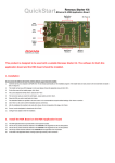
REG10J0052-0200
Renesas Starter Kit Ethernet & USB
Application Board User's Manual
RENESAS STARTER KIT
Rev.2.00
Revision date:17.Jan.2008
Renesas Technology Europe Ltd.
www.renesas.com
D007133_11
Table of Contents
Chapter 1. Preface ..................................................................................................................................................3
Chapter 2. Purpose .................................................................................................................................................4
Chapter 3. Board Layout .........................................................................................................................................5
3.1. Component References ...............................................................................................................................5
3.2. Board Component functions.........................................................................................................................6
3.3. Board Dimensions ........................................................................................................................................7
Chapter 4. User Circuitry.........................................................................................................................................8
4.1. Fitting the Target RSK to the RSK application board ...................................................................................8
4.2. Network Controller........................................................................................................................................8
4.3. USB Controller..............................................................................................................................................9
4.4. SRAM ......................................................................................................................................................... 11
4.5. Option Links................................................................................................................................................12
Chapter 5. Headers...............................................................................................................................................13
5.1. Application Headers ...................................................................................................................................13
Chapter 6. Code Development .............................................................................................................................17
Chapter 7. Additional Information..........................................................................................................................18
ii
Chapter 1. Preface
Cautions
This document may be, wholly or partially, subject to change without notice.
All rights reserved. Duplication of this document, either in whole or part is prohibited without the written permission of Renesas
Technology Europe Limited.
Trademarks
All brand or product names used in this manual are trademarks or registered trademarks of their respective companies or
organisations.
Copyright
© Renesas Technology Europe Ltd. 2007. All rights reserved.
Website:
http://www.eu.renesas.com/
Glossary
CPU
Central Processing Unit
RTE
Renesas Technology Europe Ltd.
HEW
High-performance Embedded Workshop
RSO
Renesas Solutions Organisation.
USB
Universal Serial Bus
RSK
Renesas Starter Kit
PC
Program Counter
NIC
Network Interface Controller
E10A
‘E10A for Starter Kits’ Emulator
3
Chapter 2.Purpose
This RSK Application Board is an evaluation tool for using Renesas microcontrollers with Ethernet and USB interfaces. It is used in
conjunction with the RSK for the microcontroller to be evaluated.
Features include:
•
Mounting connections to allow RSK to be added to top of board.
•
Interface to standard RSK ‘Application Interface’ connectors.
•
Interface to Memory Expansion connectors.
•
Power connector for +5V (reverse polarity protected), with on-board regulated 3.3V conversion and level translation to
allow operation with RSK boards working at either +5V or +3.3V.
•
LAN9118-MT NIC and RJ45 Ethernet connector with integral status LEDs.
•
ISP1761BE USB Hi-Speed 2.0 Host Controller with:
•
o
1 Host/Slave USB (Mini AB) connector and
o
2 Host USB (Standard A) connectors.
512 kByte Static Ram arranged as 256k x 16 bit words.
4
Chapter 3.Board Layout
3.1.Component References
The following diagram shows the component references for the board.
Figure 3-1: Component References
5
3.2.Board Component functions
The following diagram the shows the functions of the components on the board.
+5V DC
Application Board Interface
JA5
USB
JA1
J4
J1
Mini AB
USB
J5
Std A
J3
JA3
RJ45
J2
JA6
JA2
Application Board Interface
Figure 3-2: Board Layout
6
Memory Extension Interface
3.3.Board Dimensions
The following diagram gives the board dimensions and connector positions. All through hole connectors are on a common 0.1” grid for easy
interfacing.
Figure 3-3 : Board Dimensions
7
Chapter 4.User Circuitry
4.1.Fitting the Target RSK to the RSK application board
The board is supplied with 2x 24 way sockets, 2x 26 way sockets and 1 x 50 way socket.
These should be soldered on the underside of the host RSK in JA1, JA2, JA5, JA6 and JA3 positions.
The RSK should be plugged into the equivalent connectors on the RSK LCD application board.
A separate application note is available to explain how to configure the host RSK to enable it to connect to this
application board.
The board is designed to be 5V I/O tolerant. Therefore this board can be connected to an RSK with 5V I/O.
4.2.Network Controller
The network functionality is provided by the SMCS LAN9118-MT non-PCI Ethernet controller.
Refer to the manufacturer’s datasheet for more information on this peripheral.
The Ethernet controller is configured to use a 16 bit data bus. It uses single 16 bit read and write strobes.
Byte or long word accesses are not available for this device.
The chip select used for the network controller is CS1 which is on JA3 pin 27.
Please note the timing. This will require programming the bus controller for the Host RSK.
5ns
A[7:1]
0ns
40ns
CSn,RDn
0ns
35ns
Valid
Data
Figure 4-1: Ethernet controller read timing
8
5ns
A[7:1]
5ns
35ns
CSn,WRn
10ns
5ns
Valid
Data
Figure 4-2: Ethernet controller write timing
The Ethernet controller can drive two interrupts.
IRQ0 is the IRQ from the Ethernet controller.
IRQ2 is the PME output from the Ethernet controller. PME interrupts can be enabled on the IRQ pin, so this can
be disabled for host RSKs with fewer interrupt lines, if the PME interrupt is required.
Both interrupts are pulled high to 3.3V by 1K resistors.
4.3.USB Controller
The Universal Serial Bus functionality is provided by the Philips ISP1761 controller.
Refer to the manufacturer’s datasheet for more information on this peripheral.
This peripheral provides 2 Host type A and one On the Go Host/Peripheral mini AB type USB controller.
The ISP1761 controller is configured to use a 16 bit data bus. It uses single 16 bit read and write strobes.
Byte or long word accesses are not available for this device.
The chip select used for the USB controller is CS2 which is on JA3 pin 28.
Please note the timing. This will require programming the bus controller for the Host RSK.
9
5ns
A[17:1]
5ns
40ns
CSn,RDn
0ns
35ns
Valid
Data
Figure 4-3: USB controller read timing
5ns
A[17:1]
5ns
20ns
CSn,WRn
8ns
5ns
Valid
Data
Figure 4-4: USB controller write timing
The ISP1761 controller can drive two interrupts.
IRQ1 is the HC_IRQ from the ISP1761 controller.
IRQ3 is the DC_IRQ output from the ISP1761 controller. DC_IRQ interrupts can be enabled on the HC_IRQ pin,
so this can be disabled for host RSKs with fewer interrupt lines, if the DC_IRQ interrupt is required.
Both interrupts are pulled high to 3.3V by 1K resistors.
10
4.4.SRAM
The board is provided with 512 kilobytes of static RAM arranged as 256k x 16 bit words.
This RAM is byte addressable, provided the host RSK supports this.
The chip select used for the RAM is CS3 which is on JA3 pin 45.
Please note the timing. This will require programming the bus controller for the Host RSK.
5ns
A[18:1]
5ns
20ns
CSn,RDn
0ns
15ns
Valid
Data
Figure 4-5: SRAM read timing
5ns
A[18:1]
5ns
20ns
CSn,WRn
8ns
Valid
Data
Figure 4-6: SRAM write timing
11
5ns
4.5.Option Links
Table 4-1 below describes the function of the option links contained on this CPU board. The default configuration is indicated by BOLD
text.
Option Link Settings
Reference
Function
Fitted
Alternative (Removed)
Related To
R2
3V power select
Regulator drives Board_3V3
Board_3V from RSK
R7
Write Strobe Select
High Byte writes from WR1n
WR1n not connected
R8, R9, R10
R8
Write Strobe Select
High Byte writes from WR1n
WR1n not connected
R7, R9, R10
R9
Write Strobe Select
Low Byte writes from WR0n
WR0n not connected
R7, R8, R10
R10
Write Strobe Select
Low Byte writes from WR0n
WR0n not connected
R7, R8, R9
Table 4-1: JA1 Option Link Settings
12
Chapter 5.Headers
5.1.Application Headers
This information is supplied for reference. Only pins marked
are connected on this board.
These connections are not level translated.
Table 5-1 and Table 5-2 below show the standard application header connections.
JA1
Pin
Generic Header Name
CPU board
Pin
Header Name
Signal Name
CPU board
Signal Name
1
Regulated Supply 1
5V
2
Regulated Supply 1
GROUND
3
Regulated Supply 2
3V3
4
Regulated Supply 2
GROUND
5
Analogue Supply
AVcc
6
Analogue Supply
AVss
7
Analogue Reference
AVref
8
ADTRG
ADTRG
9
ADC0
I0
AD0
10
ADC1
I1
AD1
11
ADC2
I2
AD2
12
ADC3
I3
AD3
13
DAC0
DAC0
14
DAC1
DAC1
15
IOPort
IO_0
16
IOPort
IO_1
17
IOPort
IO_2
18
IOPort
IO_3
19
IOPort
IO_4
20
IOPort
IO_5
21
IOPort
IO_6
22
IOPort
IO_7
23
Open drain
IRQ3
24
I²C Bus - (3rd pin)
IIC_EX
25
I²C Bus
IIC_SDA
26
I²C Bus
IIC_SCL
IRQAEC
Table 5-1: JA1 Standard Generic Header
13
JA2
Pin
Generic Header Name
CPU board
Pin
Header Name
CPU board
Signal Name
Signal Name
1
Open drain
RESn
2
External Clock Input
EXTAL
3
Open drain
NMIn
4
Regulated Supply 1
Vss1
5
Open drain output
WDT_OVF
6
Serial Port
SCIaTX
7
Open drain
IRQ0
8
Serial Port
SCIaRX
9
Open drain
IRQ1
10
Serial Port
SCIaCK
11
Up/down
MO_UD
12
Serial Port Handshake
CTS/RTS
13
Motor control
MO_Up
14
Motor control
MO_Un
15
Motor control
MO_Vp
16
Motor control
MO_Vn
17
Motor control
MO_Wp
18
Motor control
MO_Wn
19
Output
TMR0
20
Output
TMR1
21
Input
TRIGa
22
Input
TRIGb
23
Open drain
IRQ2
24
Tristate Control
TRSTn
25
SPARE
-
26
SPARE
-
WUP
Table 5-2: JA2 Standard Generic Header
Table 5-3 and Table 5-4 below show the optional generic header connections
JA5
Pin
Generic Header Name
CPU board
Pin
Header Name
Signal Name
CPU board
Signal Name
1
ADC4
I4
AD4
2
ADC5
I5
AD5
3
ADC6
I6
AD6
4
ADC7
I7
AD7
5
CAN
CAN1TX
6
CAN
CAN1RX
7
CAN
CAN2TX
8
CAN
CAN2RX
9
Reserved
10
Reserved
11
Reserved
12
Reserved
13
Reserved
14
Reserved
15
Reserved
16
Reserved
17
Reserved
18
Reserved
19
Reserved
20
Reserved
21
Reserved
22
Reserved
23
Reserved
24
Reserved
Table 5-3: JA5 Optional Generic Header
14
JA6
Pin
Generic Header Name
CPU board
Pin
Header Name
Signal
CPU board
Signal Name
Name
1
DMA
DREQ
2
DMA
DACK
3
DMA
TEND
4
Standby (Open drain)
STBYn
5
Host Serial
RS232TX
6
Host Serial
RS232RX
7
Serial Port
SCIbRX
8
Serial Port
SCIbTX
9
Serial Port
Synchronous
SCIcTX
10
Serial Port
SCIbCK
11
Serial Port
Synchronous
SCIcCK
12
Serial Port
13
Reserved
14
Reserved
15
Reserved
16
Reserved
17
Reserved
18
Reserved
19
Reserved
20
Reserved
21
Reserved
22
Reserved
23
Reserved
24
Reserved
SCIdTX
Table 5-4: JA6 Optional Generic Header
15
SCIdRX
Synchronous
SCIcRX
Table 5-5 below shows the Memory Expansion connections
These connections support 5 to 3.3V level translation.
JA3
Pin
Generic Header Name
Signal Name
Pin
Header Name
1
A(0)
A(0)
2
A(1)
A(1)
3
A(2)
A(2)
4
A(3)
A(3)
5
A(4)
A(4)
6
A(5)
A(5)
7
A(6)
A(6)
8
A(7)
A(7)
9
A(8)
A(8)
10
A(9)
A(9)
11
A(10)
A(10)
12
A(11)
A(11)
13
A(12)
A(12)
14
A(13)
A(13)
15
A(14)
A(14)
16
A(15)
A(15)
17
D(0)
D(0)
18
D(1)
D(1)
19
D(2)
D(2)
20
D(3)
D(3)
21
D(4)
D(4)
22
D(5)
D(5)
23
D(6)
D(6)
24
D(7)
D(7)
25
RDn
RDn
26
WRn
WRn
27
CS1n
CS1n
28
CS2n
CS2n
29
D(8)
D(8)
30
D(9)
D(9)
31
D(10)
D(10)
32
D(11)
D(11)
33
D(12)
D(12)
34
D(13)
D(13)
35
D(14)
D(14)
36
D(15)
D(15)
37
A(16)
A(16)
38
A(17)
A(17)
39
A(18)
A(18)
40
A(19)
A(19)
41
A(20)
A(20)
42
A(21)
A(21)
43
A(22)
A(22)
44
SDCLK
SDCLK
45
CS3n
CS3n
46
ALE
ALE
47
WR1n
WR1n
48
WR0n
WR0n
49
CASn
CASn
50
RASn
RASn
Table 5-5: JA3 Memory Expansion connector
16
Signal Name
Chapter 6.Code Development
RSKs with appropriate connections will include suitable sample software to drive the interfaces on this board.
17
Chapter 7.Additional Information
For details on how to use High-performance Embedded Workshop (HEW), refer to the HEW manual available on the CD or from the web
site.
Online technical support and information is available at: http://www.renesas.com/renesas_starter_kits
Technical Contact Details
America:
[email protected]
Europe:
[email protected]
Japan:
[email protected]
General information on Renesas Microcontrollers can be found on the Renesas website at: http://www.renesas.com/
18
Renesas Starter Kit Ethernet & USB Application Board
User's Manual
Publication Date
Published by:
Rev.2.00
17.Jan.2008
Renesas Technology Europe Ltd.
Duke’s Meadow, Millboard Road, Bourne End
Buckinghamshire SL8 5FH, United Kingdom
©2007 Renesas Technology Europe and Renesas Solutions Corp., All Rights Reserved.
Renesas Starter Ethernet & USB
Application Board User's Manual
Renesas Technology Europe Ltd.
Duke’s Meadow, Millboard Road, Bourne End
Buckinghamshire SL8 5FH, United Kingdom