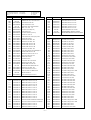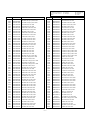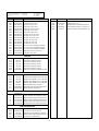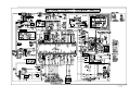
1
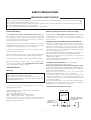
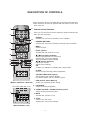
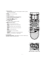
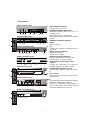
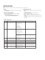
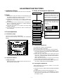
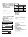
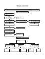
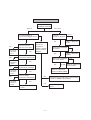
website:http://biz.LGservice.com
e-mail:http://www.LGEservice.com/techsup.html
COLOR TV
SERVICE MANUAL
CHASSIS : MC-049B
MODEL:RT-21FA35R/RX/V/VX
MODEL:RT-21FA315EX/PX
CAUTION
BEFORE SERVICING THE CHASSIS,
READ THE SAFETY PRECAUTIONS IN THIS MANUAL.
CONTENTS
Contents ...................................................................................................................2
Safety Precautions..............................................................................................3
Control Descriptions..........................................................................................4
Specifications........................................................................................................7
Adjustment Instructions .................................................................................8
Trouble Shooting.................................................................................................12
Printed circuit board.........................................................................................16
Block Diagram ......................................................................................................19
Exploded View....................................................................................................20
Exploded View Parts List ..............................................................................21
Replacement Parts List .................................................................................22
SVC. Sheet..................................................................................................................
- 2 -
SAFETY PRECAUTIONS
IMPORTANT SAFETY NOTICE
Many electrical and mechanical parts in this chassis have special safety-related characteristics. These parts are identified by
in
the Schematic Diagram and Replacement Parts List.
It is essential that these special safety parts should be replaced with the same components as recommended in this manual to
prevent X-RADIATION, Shock, Fire, or other Hazards.
Do not modify the original design without permission of manufacturer.
General Guidance
Before returning the receiver to the customer,
An isolation Transformer should always be used during
the servicing of a receiver whose chassis is not isolated from
the AC power line. Use a transformer of adequate power rating
as this protects the technician from accidents resulting in
personal injury from electrical shocks.
always perform an AC leakage current check on the exposed
metallic parts of the cabinet, such as antennas, terminals, etc.,
to be sure the set is safe to operate without damage of
electrical shock.
Leakage Current Cold Check(Antenna Cold Check)
It will also protect the receiver and it's components from being
damaged by accidental shorts of the circuitry that may be
inadvertently introduced during the service operation.
If any fuse (or Fusible Resistor) in this TV receiver is blown,
replace it with the specified.
When replacing a high wattage resistor (Oxide Metal Film
Resistor, over 1W), keep the resistor 10mm away from PCB.
Keep wires away from high voltage or high temperature parts.
Due to high vacuum and large surface area of picture tube,
extreme care should be used in handling the Picture Tube.
Do not lift the Picture tube by it's Neck.
X-RAY Radiation
Warning:
The source of X-RAY RADIATION in this TV receiver is the
High Voltage Section and the Picture Tube.
For continued X-RAY RADIATION protection, the
replacement tube must be the same type tube as specified in
the Replacement Parts List.
To determine the presence of high voltage, use an accurate
high impedance HV meter.
With the instrument AC plug removed from AC source,
connect an electrical jumper across the two AC plug prongs.
Place the AC switch in the on position, connect one lead of
ohm-meter to the AC plug prongs tied together and touch other
ohm-meter lead in turn to each exposed metallic parts such as
antenna terminals, phone jacks, etc.
If the exposed metallic part has a return path to the chassis, the
measured resistance should be between 1MΩ and 5.2MΩ.
When the exposed metal has no return path to the chassis the
reading must be infinite.
An other abnormality exists that must be corrected before the
receiver is returned to the customer.
Leakage Current Hot Check (See below Figure)
Plug the AC cord directly into the AC outlet.
Do not use a line Isolation Transformer during this check.
Connect 1.5K/10watt resistor in parallel with a 0.15uF capacitor
between a known good earth ground (Water Pipe, Conduit, etc.)
and the exposed metallic parts.
Measure the AC voltage across the resistor using AC
voltmeter with 1000 ohms/volt or more sensitivity.
Reverse plug the AC cord into the AC outlet and repeat AC
voltage measurements for each exposed metallic part. Any
voltage measured must not exceed 0.75 volt RMS which is
corresponds to 0.5mA.
In case any measurement is out of the limits specified, there is
possibility of shock hazard and the set must be checked and
repaired before it is returned to the customer.
Leakage Current Hot Check circuit
Adjust brightness, color, contrast controls to minimum.
Measure the high voltage.
The meter reading should indicate
23.5 ¡ 1.5KV: 14-19 inch, 26 ¡ 1.5KV: 19-21 inch,
29.0 ¡ 1.5KV: 25-29 inch, 30.0 ¡ 1.5KV: 32 inch
If the meter indication is out of tolerance, immediate service
and correction is required to prevent the possibility of
premature component failure.
AC Volt-meter
To Instrument's
exposed
METALLIC PARTS
Good Earth Ground
such as WATER PIPE,
CONDUIT etc.
0.15uF
1.5 Kohm/10W
- 3 -
DESCRIPTION OF CONTROLS
All the functions can be controlled with the remote control handset.
Some functions can also be adjusted with the buttons on the front
panel of the set.
POWER
MUTE
1
11
2
1
2
3
4
5
6
7
8
9
0
TV/AV
PICTURE
MENU
SOUND
10
OK
T U R B O
Before you use the remote control handset, please install the batteries. See the next page.
1. POWER
switches the set on from standby or off to standby.
12
3 2. NUMBER BUTTONS
switches the set on from standby or directly select a number.
3. MENU
selects a menu.
( )
PR
5
VOL
VOL
Remote control handset
PR
( )
18
13
8
15
19
REW
PLAY
FF
P/STILL
STOP
REC
I/II
SSM
PSM
SLEEP
PIP
LIST
EYE/
FAVOURITE Q.VIEW
4. EYE/ (option)
switches the eye function on or off.
*
5.
14
16
4
6
9
SIZE
STILL
POSITION
9/4PIP
PR
PR
SWAP
INPUT
D / E (Programme Up/Down)
selects a programme or a menu item.
switches the set on from standby.
scans programmes automatically.
F / G (Volume Up/Down)
adjusts the volume.
adjusts menu settings.
OK
accepts your selection or displays the current mode.
6. Q.VIEW
returns to the previously viewed programme.
7. TELETEXT BUTTONS (option)
These buttons are used for teletext.
For further details, see the ÔTeletextÕ section.
(Without TELETEXT / With PIP)
PSM
SLEEP
EYE/
FAVOURITE Q.VIEW
PIP
TEXT/
8. PSM (Picture Status Memory)
recalls your preferred picture setting.
9. FAVOURITE
selects a favorite programme.
10. TURBO PICTURE / SOUND BUTTON (option)
selects Turbo picture and sound.
7
MIX
TIME
REVEAL ? MODE M
SIZE
STILL
POSITION
PR
PR
SWAP
9/4PIP i
INPUT
11. MUTE
switches the sound on or off.
12. TV/AV
selects TV or AV mode.
switches the set on from standby.
(With TELETEXT / PIP)
- 4 -
13. I/II/ (option)
selects the language during dual language broadcast. (option)
selects the sound output.
*
POWER
14. LIST
displays the programme table.
MUTE
11
1
15. SLEEP
sets the sleep timer.
1
2
3
4
5
6
7
8
9
MENU/INDEX
0
TV/AV
2
16. SSM/ (option) (Sound Status Memory)
recalls your preferred sound setting.
*
º/ ) (option)
17. SURROUND (º
selects surround sound.
*
3
18. VCR BUTTONS
control a LG video cassette recorder.
12
TV
4
19. PIP BUTTONS (option)
PIP
switches the sub picture on or off.
PR +/selects a programme for the sub picture.
SWAP
alternates between main and sub picture.
INPUT
selects the input mode for the sub picture.
SIZE
adjusts the sub picture size.
STILL
freezes motion of the sub picture.
POSITION
relocates the sub picture in clockwise direction.
9/4 PIP
5
EYE/
PR
VOL
I / II /
( )
VOL
OK
PR
13
( )
Q.VIE
LIST
W
14
6
PSM
SSM/
SLEEP
8
FAVOURITE
/
9
PICTURE
SOUND
15
16
17
TURBO/
10
switches on or off the 9 or 4 sub pictures.
*
: No function
COLOURED BUTTONS : These buttons are used for teletext (only
TELETEXT models) or programme edit.
(Without TELETEXT / PIP)
Q.VIE
LIST
W
TEXT/MIX/
SIZE/
HOLD/
7
UPDATE/ X
PSM
TIME/
REVEAL/ ?
SSM/
SLEEP/ M
FAVOURITE PICTURE
TURBO/
SOUND
/
(With TELETEXT / Without PIP)
- 5 -
Front panel
RF/RT-21FA35 series
1. MAIN POWER (ON/OFF)
switches the set on or off.
MENU OK
VOL
PR
ON/OFF
2. POWER/STANDBY INDICATOR
illuminates brightly when the set is in
standby mode.
dims when the set is switched on.
blinks when signal is input from the remote
control.
L/MONO
2
4
1 2 3
5
RF/RT-21FB25 series
7
6
AV2
MENU
VOL
OK
PR
ON/OFF
7
1
2 3
4 5
8
4. MENU
selects a menu.
8
5. OK
accepts your selection or displays the current mode.
F / G (Volume Up/Down)
adjusts the volume.
adjusts menu settings.
D / E (Programme Up/Down)
selects a programme or a menu item.
switches the set on from standby.
RF/RT-15/21FB55 series
VIDEO
6
L/MONO AUDIO
R
3. REMOTE CONTROL SENSOR
OK
MENU
VOL
VIDEO
PR
L AUDIO R
ON/OFF
AV
1
2 3 4
6 7
5
RF/RT-17/21FB75 series
1
23
4
6. AUDIO/VIDEO IN SOCKETS (AV2)
(option)
Connect the audio/video out sockets of
external equipment to these sockets.
5
RF/RT-21FC45 series
7. HEADPHONE SOCKET (option)
Connect the headphone plug to this socket.
7
L AUDIO R
6
24
1
5
38
VIDEO
RF/RT-21FB35 series
AV2
ON/OFF
MENU OK
VOL
PR
AV
VIDEO AUDIO
Note :
a. Do not place any heavy objects (over 4Kg) on
the RF/RT-21FA35 series models.
b. Shown is a simplified representation of
front or side panel. Here shown may be
somewhat different from your set.
VIDEO L/MONO AUDIO R
AV3
1
2 3 4
5
6 7
8. EYE (option)
adjusts picture according to the surrounding conditions.
6 7
RF/RT-15/21FB95 series
AV2
7
VIDEO
L
1 23 4
5
8
AUDIO
6
R
- 6 -
SPECIFICATIONS
Note : Specification and others are subject to change without notice for improvement.
F Scope
This specification can be applied to all the television related to
MC-049B Chassis.
F Requirement for Test
Testing for standard of each par must be followed in below
condition
1) Temperature : 20 ± 5¡C
(CST must be tested 40 ± 5¡C . Humidity : 50%)
2) Relative Humidity : 65 ± 10%
3) Power : Standard input Voltage (110-240V~, 50/60Hz)
4) Measurement must be performed after heat-run more than
20min.
5) Adjusting Standard for this chassis is followed a special
standard.
F Test and Inspection Method
1) Capacity : Follow LG electronics TV testing Standard.
2) Another Required Standard
- EMI : Following CE Standard (EN55020, EN55013)
- Safety : Following CB Standard (EN55013)
F General Specification
Item
No
1
Receiving System
Specification
1) PAL/SECAM BG
Remark
For EU/ For Non EU
2) PAL/SECAM DK
3) PAL I/I
4) NTSC M
5) SECAM-L/LÕ
6) NTSC 4.43(AV)
2
Receiving Channel
1) VHF : E2 ~ E12
For EU/ For Non EU
UHF : E21 ~ E69
CATV : S1 ~ S20
HYPER : S21 ~ S41
2) L/LÕ : B,C,D
3) VHF : 02 ~ 13
NTSC-M (Multi - model)
UHF : 14~ 69
CATV : 02 ~ 71
3
Input Voltage
110-240V~, 50/60Hz
240V~, 50Hz
EU
4
Market
EU,CIS, China, Asia, Africa
5
Screen Size
14Ó ~ 21Ó
6
Tuning System
FVS 100Program
7
Operating Environment
1) Temp. : 0 ~ 45 deg
FLAT / CONVENTIONAL
2) Humidity: 85% under
8
Storage Environment
Non EU
1) Temp. : -20 ~ 60 deg
2) Humidity: 85% under
- 7 -
200 PR. (OPTION)
ADJUSTMENT INSTRUCTIONS
1. Application Object
4. Purity & Convergence adjustment
These instructions are applied to all of the color TV, MC-049B.
CPT Assembling
As preparatory operations before
assembling CPT, wind cotton Tape for
protecting to CPT NECK and DY, CPT
connection parts. At this moment, end
of tape should be over-lapped and
wound in direct route to the NECK.
Assembling DY to
CPT
Fix the Magnet to the position as
shown picture below. Be careful not to
make CPT neck shadow while
adjusting DY.
2. Notes
(1) Because this is not a hot chassis, it is not necessary to use
an isolation transformer. However, the use of isolation
transformer will help protect test instrument.
(2) Adjustment must be done in the correct order.But the
adjustment can be changed by consideration of mass
production.
(3) The adjustment must be performed in the circumstance of
25±5¡C of temperature and 65±10% of relative humidity if
there is no specific designation.
(4) The input AC voltage of the receiver must keep rating
voltage in adjusting.
(5) The receiver must be operated for about 15 minutes prior
to the adjustment.
HEAT RUN
Degaussing
Convergence Magnet
2
¢‚
¢‚
3. Focus adjustment
15 ~ 20mm
SCREEN Voltage adj.
Let the screen Standard condition.
Operate Heat-Run at least 15
minutes.
W/B Fixing
Torque is to be 9-11 kg f.cm when
fixing DY.
DY Fixing
Tune the TV set to receive a digital pattern.
(SVC mode:Automatically mode change the STANDARD
MODE)
4
STC Adjustment
PURITY Adjustment
3.1. Preliminary steps
6Pole
FOCUS not yet ADJ.
STC not yet ADJ.
DYC not yet ADJ.
A
B
4.1. Color purity adjustment
(1) It makes CPT enough to demagnetization.
(2) Receive the signal of red raster.
(3) Loosen fixed screw of DY and closely to CPT funnel part.
(4) Check the center of screen that PURITY MAGNET of CPT
by crossing adjustment. At this time, 4 & 6 pole magnet is
located to magnet of nothing.
(5) Move the DY to make equal red on whole screen and it
does not to make the DY by fixed screw after check a
simple color of Red/Green/Blue and white raster whether or
not it is a pollution of color.
(At this time, take care raster of screen and DY must fixing
in the condition which maintains a horizontality.)
(6) Check the receiver by move direction. When adjustment is
not working, adjust with the assisted MAGNET.
<Fig 1. PAL Digital Pattern(EU05CH)>
3.2. Adjustment Method
1) Single Focus CPT
Adjust the upper Focus volume of FBT for the best focus of
horizontal line A,vertical line B.
4.2. Convergence adjustment
These adjustments can the best condition of focus after
finished purity adjustment.
(1) Receive the signal of CROSS HATCH that BACK RASTER
is black.
(2) Adjust brightness and luminosity till dot appear 9 ~12.
(3) Open angle of the two tab of 4 pole MAGNET by isogonic
angle and accord with vertical line of red and blue color in
the middle of screen.
- 8 -
(4) Maintain as angle of (3) and rotate the tab to accord with
vertical line of Red and Blue color in the middle of screen.
(5) Open angle of the two tab of 6 pole magnet by isogonic
angle and accord with vertical line of Red/Blue and Green.
(6) Maintain as angle of (5) and rotate the tab to accord with
horizontal line. In case of twisted horizontal line,repeat
adjustment of (3) ~ (5) remembering the movement of
Red/Green/Blue color.
(7) Move the DY to best condition of convergence and attach
the CPT to a rubber-chock for fixed DY.
2. White balance IIC Parameter
Program
TWBeng_v049
Program
TWBeng_v049
Speed
Delay
Vcd Slave
BCF0
Eprom_Slave
AE
1
30
R_Amp
Program
5. Screen voltage adjustment
(1) Receive the PAL or SECAM(NTSC) signal into RF mode
regardless of channel.
(2) If you press the ÒADJÓbutton in LINE SVC mode(IN-START
button),the LINE SVC mode changes to screen adjustment
mode.
(3) Adjust the screen volume of FBT jack,When width line is
seen turn the FBT screen volume at the position of
disappearance it.
(4) Press the TV/AV button to exit SVC mode.
6. White balance adjustment
NOTE : When adjusting white balance automatically,connect the
adjustment JIG in SVC mode.(When pressing ,MUTE
button on remote control, it changes to CPU OFF MODE
and screen displays ÒAUTOÓ.)
R_Cut
B_Amp
B_Cut
TWBeng_v049 TWBeng_v049 TWBeng_v049 TWBeng_v049
Sub Add
1C8
1C3
1CA
1C5
Start Bit
12
12
12
12
Stop Bit
4
4
4
4
Offset
0
0
0
0
Polarity
1
1
1
1
EP_Rom_S
9091
8A8B
9495
8E8F
Speed/ Plus
1
1
1
1
<CAUTION> W/B Program ÒTwbeng_v049Ó
- W/B adjustment after Cutoff
: Instart -> adj. -> mute(cutoff)-> tv/av(wb)
Release key is EXIT key
- W/B adjustment
: Instart -> mute(cpuoff)
Release key is TV/AV key
7.Deflection setting Data Adjustment
7.1 Adjustment preparation
(1) Tune the TV set to receive an Digital pattern(EU05CH).
(2) Deflection setting data adjustment is operate by SVC
communicator.
(3) Enter the deflection adjustment mode by selection
SERVICE1 on SERVICE MENU after pressing LINE SVC
MODE(IN-START KEY).
(4) Use the CH D ,E key to select adjustment item.
(5) Use the VOL F ,G key to increase/decrease data.
(1) Receive 100% white pattern.
(2) Adjust LOW Light status(4.5FL) of CUT R,CUT B at CG:60.
(3) Adjust HIGH LIght status(35FL) of WDR R,WDR B at
WDR G:450.
(4) Repeat above step (2) and (3) for the best condition each
status of High Light and Low Light.
<Table 1> White Balance Color analyzer
Menu
EU
N-EU
X
288
266
Y
295
273
Color Temperature
9000¡K
13000¡K
<Table 2> White Balance Initial Data
Menu
Menu
Range
DATA
LOW LIGHT
CUT R
0 ~ 511
60
CUT G
0 ~ 511
60
CUT B
0 ~ 511
60
HIGH LIGHT
WDR R
0 ~ 511
450
WDR G
0 ~ 511
450
WDR B
0 ~ 511
450
<Note>
(1) When adjusting a deflection, adjust N50Hz of PAL signal
first and adjust a deflection at Normal 60Hz(NTSC).
(2) Adjust a deflection as shown below.
PAL 4:3 -> NTSC 4:3
(3) After finishing deflection adjustment, press the ENTER key
to exit in adjustment mode.
* Before adjusting the PIP P(PIP Position), store the
deflection data in the EEPROM by using the ÒENTERÓ key.
7.2 Adjustment
(1) VL(Vertical Linearity) adjustment:
Adjust the top & bottom size of inner circle to be equal.
(2) VA (Vertical Amplitude) adjustment:
Adjust so that the circle of a digital circle pattern should be
located interval of 6~7mm from the effective screen of the
CPT.
(3) SC (S correction) adjustment:
Adjust so that all distance between each lattice width of
top/center/bottom are to be the same.
* Auto adjustment
<Table 3> White Balance Initial Data
1. IC
VCD IC
EP_ROM
Name
Maker
VCT49xyi
Micronas
24C16
ST, ATMEL
Algorithm
0
A
* Setting the CPT Default(Initial data) value like that, because
it is decide by CPT DY value
0
- 9 -
(4) VS (Vertical Shift) adjustment:
Adjust so that the geometric vertical center line is in accord
with vertical center line of CPT.
(5) HS(Horizontal Shift) adjustment:
Adjust so that the geometric horizontal center line is in
accord with horizontal center line of CPT.
8-4. OPTION2 Function
Option
Code
AV2
0
Without A/V2
1
With AV2
0
Without DVD
1
With DVD
0
Without SCART1
1
With SCART1
0
Without GAME function
1
With GAME function
0
Without EYE
1
With EYE
0
LARGE
1
SMALL
0
6,8 KEY
1
4 KEY
0
Without DEGAU
1
Whit DEGAU
DVD
<Table 4> Initial deflection setting data
Menu
N50Hz(PAL)
Variable range
FLAT 21Ó
N60Hz(NTSC)
FLAT 21Ó
VS
-512~511
150
140
VA
-512~511
-12
-12
VL
-512~511
140
140
SC
-512~511
6
6
HS
32~2047
100
SCART1
GAME
EYE
TX
123
KEY
8.OPTION Adjustment
DEGAU
8-1. Preparation for Adjustment
1) This option adjustment decides function in accordance with
model. Press IN-START button on SVC communicator,
then adjust the option at OPTION1 mode.
2) Mark the option adjustment data like [111,111,111,111] in
BOM.
8-2. Adjustment Method
OPTION data input
1) Function : YES, No function : NO
2) Select each OPTION function by the CH Up/Down
button and then set up each OPTION(yes or no) by the
VOL Up/Down button.
8-3. OPTION 1
Option
Code
INCH
0
SYS
SOUND
CH+AU
8-5. OPTION3 Function
Option
Code
TEXT
0
Without TEXT (200PR)
1
With TEXT (100PR)
0
FLOP
1
TOP
0
Without ACMS
1
With ACMS
0
Without I 2 SV
1
With I 2 SV
0
VOL 0
1
VOL 1
0
Without TURBO SEARCH
1
With TURBO SEARCH
0
Without TURBO PICTURE/ SOUND
1
With TURBO PICTURE/ SOUND
0
Without HDEV
1
With HDEV
TOP
ACMS
I 2 SV
Function
VOL
21A
1
21B
2
21C
3
29F/25F
4
28WF/32WF
5
28N
6
34F
7
29N/25N
0
BG/I/DK
1
BG/I/DK/L
2
BG/I/DK/M
3
BG/L
0
RF STEREO
1
AV STEREO
2
MONO
3
MONO DUAL
0
Using
1
Not using
Function
TSEAR
T P-S
HDEV
- 10 -
Function
8-6. OPTION4 Function
Option
Code
OSD L
0
ENG ONLY
1
EU-5EA
2
EU ETC
3
GREECE
4
EU-ALL
5
FARSI
6
ARAB URDU
7
E+HINDI
8
E+I+M+V
9
E+THAI
10
E+CHINA
0
WEST EU
1
EAST EU1
2
TURKEY EU
3
EAST EU2
4
CYRILLIC1
5
CYRILLIC2
6
CYRILLIC3
7
TURK GRE1
8
TURK GRE2
TXT L
Function
9
TURK GRE3
10
ARAB FRA
11
ARAB ENG
12
ARAB HEB1
13
ARAB HEB2
14
FARS ENG
15
FARS FA
16
FARS ALL
17
AUTO
HOTEL
0
WITHOUT HDEV
1
WITH HDEV
MAX V
0~
SETTING VOL MAX
100
- 11 -
TROUBLE SHOOTING
RF- STEREO
MODEL
PICTURE O. K / NO SOUND
Selec t ed c o rrec t syst em
In m enu
OK
Chec k t he wavef o rm
IF 1 o f TU101
NO
Chec k / Rep lac e
TU 101
NO
NO
Chec k The Vo lt ag e
At p in 2, 19 , 20, 2 1, 24 o f IIC11
OK
Chec k t he wavef o rm
At p in 4, 5 o f IC11
Chec k The vo lt ag e
At p in o f IC82 1, IC8 22, Q807
OK
NO
Chec k t he wavef o rm
At p in 2, 4 o f IC601
Chec k / Rep la c e
C821, IC822, Q80 7
OK
Chec k t he wavef o rm
At p in 6 o f IC60 1
NO
Chec k / Rep lac e Q60 1
OK
Chec k t he wavef o rm
At p in 8, 9, 1 1, 12 o f IC601
OK
Chec k t he wavef o rm
At p in 5, 6 o f IC601
NO
Chec k / Rep lac e
F80 6, D8 28( D805)
No Rast er / So und OK ( 1/ 2)
Chec k t he
Heat er vo lt ag e o f CPT
( 6 ~ 6. 4 Vrm s)
Chec k
HV, Sc reen Vo lt ag e o f
CPT
Chec k
FBT T4 02
Chec k 185V line o f CPT
Bo ard & if no p ro b lem
c hec k and Rep lac e
Chec k
R, G, B o ut o f
CPT Bo ard
Chec k
IC901 , P903 A
- 12 -
Chec k t he
Heat er p ulse o f FBT
T402
Chec k
RF901 , P4 02
P4 02B, FR401
Chec k
FBT T402
No Ras ter ( 2/ 2)
CHECK B+
At D829 c at ho d e
No rm al
Ab no rm al
Is t he vo lt ag e a t
eac h p in vo lag e o f IC11
NO
Chec k &
Rep lac e
IC11
NO
Chec k &
Rep lac e
Q40 2
NO
Chec k &
Rep lac e
T40 1
NO
Chec k &
Rep lac e
Q40 1
Chec k p in 60
Of IC1 1( H - Out )
Yes
Op en
Chec k
Fuse o f AC line
Chec k t he
In/ o ut o f
reg ulat o r
( IC8 21, IC822
IC82 3, IC824
IC82 5)
Chec k / Rep lac e
Fuse
OK
Chec k / Rep lac e
DB801
OK
Chec k Q40 2
Co llec to r wavef o rm
NO
Chec k t he Vo lta g e
Of C803
NO
Chec k t he Vo lta g e
Pin 4 OF IC801
Yes
OK
Chec k T401
& eac h p in vo lta g e
Chec k / Rep lac e
Fuse IC8 01
Chec k / Rep lac e
IC8 01, IC802 , IC826
Yes
Chec k Q40 1
Co llec to r wavef o rm
18~20V
NO
Chec k Fuse and Dio d e o f sec o nd ary
Lo ad o f SMPS t rans( T803)
Yes
OK
Chec k & Rep lac e
T402
- 13 -
Chec k / Rep lac e
IC1 1
NO Pic t ure / No So und
Is Any OSD d isp la yed ?
OK
OK
Chec k IC11 p in71, 7 2, 73
( R, G, B o ut )
Chec k rec eiving syst em in MENU
& exec ut e Aut o - Pro g ram .
OK
Do es t he auto - Pro g ra m
Op erat e p ro p erly
NO
OK
Sto re o n m anual- p ro g ram MENU
Chec k p in40( V o ut 1)
1 Vp - p
NO
Chec k 1 . 8V , 3. 3 V,
5 V DC Vo ltag e
Chec k p in18
Reset Vo lta g e
3.3 V DC
NO
NO
Chec k SMPS Trans
Sec o nd ary Vo ltag e
Chec k IC13
( Reset IC)
OK
Chec k p in57, 58
SCL, SDA
3.3 V DC
NO
NO
Chec k IC12 ( EEPROM)
& SCL , SDA Line
OK
Relac e IC11
Q501 , Q5 03, Q50 4
( R, G, B o ut o f IC11)
Chec k / Rep la c e
CPT Bo ard c o m p o nent
- 14 -
Go t o
No So und /
Pic t ure OK
AV STERRO / MONO MODEL
Selec t c o rrec t syst em
In m enu
OK
OK
Chec k t he c o nnec t io n
Of AV eq uip m ent
AV
Chec k t he wavef o rm
At p in16, 17 o f IC11
OK
NO
Chec k TU1 01 Tuner
OK
NO
Chec k t he vo lt ag e
Of p in2 , 19, 20, 21, 2 4 o f IC11
Chec k t he wavef o rm
At p in4 , 5 o f IC11
OK
NO
Chec k t he wavef o rm
At p in2 , 4 o f IC601
Chec k t he sig na l line o f
SPK- L, R
OK
NO
Chec k t he wavef o rm
At p in6 o f IC601
Chec k p in 55 ( m ut e)
o f IC11
OK
Chec k t he wavef o rm
At p in8 , 9, 11, 12 o f IC6 01
NO
Chec k t hevp lta g e
At p in7 , 5 o f IC601
NO
Chec k/ Rep lac e
D828, D805, F8 06
OK
Chec k t he c o nnec t io n o f NO
sid e o r Fro nt AV Bo a rd
P603A
OK
Rep la c e IC601
- 15 -
Co rrec t t he Bo ard
PRINTED CIRCUIT BOARD
MAIN
- 16 -
COMPONENT LOCATION GUIDE
ffdf
C10 ........C4
C11 ........C4
C12 ........C4
C13 ........C3
C14.........F1
C16 ........C2
C21.........E1
C22.........B2
C23.........A4
C24.........A3
C25.........B4
C101.......A5
C102.......F1
C103 ......C1
C104.......A5
C105.......A5
C106.......B4
C107.......B5
C108.......B5
C109.......B4
C110.......B4
C111.......A5
C126.......A4
C185 ......C1
C201 ......D5
C202 ......D5
C203 ......C5
C204 ......C5
C205.......E5
C206 ......C5
C207.......B5
C209.......B5
C210.......E5
C211 ......D5
C214 ......D5
C215 ......D5
C216 ......C5
C217 ......D5
C224 ......D5
C225 ......D5
C226 ......D5
C251 ......C1
C252.......B1
C253 ......C1
C254 ......C1
C255 ......C1
C256 ......C1
C259 ......C1
C260 ......C1
C261 ......C1
C301.......E4
C302.......E4
C303.......E4
C304 ......D4
C306.......F4
C307 ......D4
C308 ......D3
C401 ......D3
C402 ......G4
C403 ......G3
C404.......F3
C405 ......G3
C409.......F4
C410.......F3
C411.......F3
C412.......F4
C414.......E5
C415.......E4
C416.......E5
C417.......E5
C419.......E4
C421.......E5
C422.......E5
C450.......E5
C457 ......D5
C501.......B4
C502.......B4
C503 ......D4
C504.......B4
C505 ......C3
C506 ......C3
C507 ......C3
C508 ......C3
C509.......B4
C510.......B3
C511 ......C4
C512.......B3
C513 ......C4
C514 ......C5
C515.......B3
C516.......B3
C517 ......C4
C518.......B3
C519 ......C4
C520 ......C4
C521 ......C4
C522 ......C4
C523 ......C4
C524 ......C5
C525 ......C4
C526 ......C4
C527 ......C4
C528 ......C4
C529 ......C4
C530 ......C4
C531 ......C3
C532 ......C4
C533 ......C4
C534.......B4
C535.......B4
C536.......B4
C537.......B4
C538.......B4
C539 ......C5
C540.......B4
C541 ......C3
C542.......B5
C543 ......C5
C544 ......C3
C545 ......C4
C546.......B2
C547.......B2
C548 ......C4
C549 ......C1
C550 ......C4
C551 ......C4
C601.......A3
C602.......B2
C603.......A3
C604.......A3
C605.......A2
C606.......B2
C607.......A3
C608.......B2
C609.......A4
C610.......A3
C611.......A3
C612.......B2
C613.......B2
C614.......B2
C615.......B4
C616.......A4
C617.......B4
C618.......A4
C619.......A4
C620.......A4
C621.......A3
C622.......A3
C623.......A2
C625 ......D5
C626 ......D5
C627.......A2
C632 ......D4
C636 ......D4
C801 ......G1
C803.......F2
C804 ......G2
C806 ......G2
C807.......F3
C808.......F3
C809.......F2
C810.......F2
C811.......F2
C815.......F3
C816.......F1
C817 ......G3
C818 ......G1
C819 ......G3
C820 ......D1
C821.......E2
C822.......E2
C823.......E1
C824 ......D1
C826 ......D1
C827 ......D2
C828 ......D2
C829 ......D2
C830 ......D2
C831 ......D3
C833 ......D3
C834 ......D3
C835.......E3
C836.......E3
C837.......E3
C838.......E3
C839 ......D2
C840.......E2
C841 ......G3
C842 ......G3
C843 ......G3
C844.......F2
C845 ......D1
C846.......E3
C847 ......D3
C848 ......D3
C849 ......D3
C868 ......D3
C901.......B1
C902.......A1
C903.......A2
C904.......B2
C905.......A1
C906.......B1
D101.......A4
D301.......E4
D402 ......G3
D403.......F3
D405.......E4
D406.......E5
D407.......E5
D444.......E5
D501.......B3
D502.......B2
D503.......B3
D504 ......D4
D601.......B2
D602.......A3
D603.......A2
D604.......A3
D801.......F3
D802.......F3
D803.......F3
D805.......E3
D815 ......G2
D821.......E2
D823.......E1
D827 ......D2
D828 ......D2
D829 ......D3
D830.......E3
D854.......E1
D901.......A1
D902.......A1
D903.......A1
D904.......B2
DB801....G2
HIC01.....C2
IC11........B4
IC12........A4
IC13........B4
IC301......E4
IC601......A3
IC801 .....G2
IC802......F3
IC821 .....D2
IC822......E1
IC824......E1
IC825 .....D1
IC826 .....D3
IC853......E1
IC901......A1
J11 .........A4
J102 .......B4
J103 .......C1
J104 .......A5
J105 .......B5
J107 .......A5
J108 .......B1
J109 .......A5
J110 .......B3
J111 .......B4
J112 .......B5
J113 .......A5
J114 .......C2
J115 .......C1
J116 .......A5
J117 .......A5
J118 .......B5
J119 .......B5
J120 .......C1
J121 .......C2
J181 .......C1
J182 .......C1
J183 .......C1
J201 .......D5
J202 .......D5
J203 .......D5
J204 .......D5
J205 .......D5
J206 .......C3
J207 .......D5
J208 .......C1
J209 .......D4
J210 .......C5
J211 .......C5
J212 .......E5
J213 .......D5
J214 .......D5
J215 .......B5
J216 .......D5
J217 .......B5
J219 .......D4
J220 .......D5
J221 .......D5
J222 .......D5
J223 .......B5
J224 .......B5
J225 .......E5
J226 .......C1
J230 .......C1
J231 .......C1
J232 .......D1
J233 .......C1
J234 .......C1
J235 .......C1
J242 .......D1
J261 .......C5
J301 .......C4
J302 .......D4
J303 .......E4
J306 .......D4
J308 .......B2
J309 .......B2
J310 .......B2
J311 .......E4
J313 .......E4
J314 .......E4
J315 .......D4
J317 .......C3
J318 .......C3
J334 .......C1
J401 .......E5
J402 .......E5
J403 .......E5
J404........F5
J405 .......D3
J408 .......E4
J409........F4
J410........F5
J412........F4
J413 .......E5
J414 .......E4
J415 .......E3
J416 .......G3
J417 .......E3
J501 .......C2
J502 .......C3
J503 .......C3
J504 .......C3
J505 .......D4
J506 .......D4
J507 .......C2
J508 .......A4
J509 .......D4
J510 .......D4
J511 .......B3
J512 .......C4
J513 .......C2
J514 .......C2
J515 .......C2
J516 .......B4
J517 .......C2
J518 .......C2
J519 .......C3
J520 .......B3
J521 .......C3
J522 .......B3
J523 .......C3
J524 .......C3
J525 .......C3
J526 .......C3
J527 .......C3
J528 .......C3
J529 .......B3
J530 .......B3
J531 .......B3
J532 .......B3
J533 .......B2
J534 .......C2
J535 .......C1
J536 .......B4
J537 .......C5
J538 .......C4
J539 .......C4
J540 .......B2
J541 .......B3
J542 .......B3
J543 .......B3
J544 .......B3
J545 .......C2
J546 .......B3
J547 .......B3
J548 .......B3
J549 .......C2
J550 .......B3
J551 .......B3
J552 .......B3
J553 .......B3
J554 .......B3
J555 .......B3
J556 .......B3
J557 .......B3
J558 .......C3
J559 .......B3
J560 .......B3
J561 .......C5
J562 .......C5
J564 .......C4
J565 .......C4
J566 .......C4
J567 .......C4
J568 .......C4
J569 .......B4
J570 .......C4
J571 .......B4
J572 .......C3
J573 .......C4
J574 .......B3
J575 .......D1
J576 .......B3
J577 .......B3
J578 .......B3
J579 .......B3
J580 .......D4
J581 .......C2
J582 .......C3
J583 .......D2
J584 .......D2
J585 .......B2
J586 .......C5
J587 .......C4
J588 .......C4
J589 .......B4
J590 .......B4
J591 .......C4
J601 .......A3
J602 .......A3
J603 .......A4
J604 .......A3
J605 .......B4
J606 .......A2
J607 .......A2
J608 .......B2
J609 .......A4
J610 .......B2
J611 .......B2
J613 .......B2
J614 .......B2
J615 .......A2
J616 .......B4
J617 .......B4
J801 .......D2
J802 .......G1
J803 .......G1
J804 .......G1
J805 .......G1
J806........F1
J807........F1
J808........F1
J809........F2
- 17 -
J810 .......D2
J811 .......D2
J812 .......E2
J813 .......D2
J814 .......D3
J815 .......G3
J816........F3
J817 .......D3
J819........F3
J820 .......D3
J821 .......D2
J822 .......E2
J823 .......E1
J824 .......D2
J825 .......D2
J826 .......D2
J827 .......D2
J828 .......D1
J829 .......D2
J830 .......E1
J832 .......E1
J833 .......D3
J834 .......D3
J835 .......D3
J836 .......D2
J838 .......D1
J840 .......D2
J841 .......E2
J842 .......E2
J901 .......A1
J902 .......A2
J903 .......B1
J904 .......B1
JK202.....C5
JP1.........G2
JP2 .........F2
JW1........G1
JW2 ........B5
Q11 ........E1
Q41 ........C2
Q42 ........C2
Q102 ......A5
Q103 ......A5
Q104 ......B4
Q105 ......A4
Q106 ......A4
Q301 ......D4
Q401 ......G4
Q402 ......G3
Q403 ......D4
Q501 ......B3
Q502 ......B2
Q503 ......C2
Q504 ......C2
Q505 ......C5
Q507 ......B5
Q508 ......B2
Q510 ......B2
Q601 ......A2
Q801 ......D3
Q802 ......D1
Q803 ......D1
Q804 ......D2
Q805 ......E1
Q807 ......D2
Q808 ......D2
R10 ........C2
R11 ........C2
R12 ........C4
R13.........E1
R14 ........D1
R15.........F1
R16.........E1
R17.........E1
R18 ........D1
R19 ........D1
R20 ........D1
R24.........B3
R25.........B3
R26 ........C2
R27 ........C2
R28.........A5
R29 ........C3
R30 ........C3
R31 ........C3
R32 ........D1
R33 ........C3
R34 ........C5
R35 ........C4
R36 ........C2
R37 ........D1
R38.........B4
R39 ........C2
R42 ........D1
R101.......A5
R102.......A5
R103.......A4
R104.......A4
R105.......A5
R106.......B5
R107.......A5
R108.......A5
R109.......B4
R110.......B4
R111.......B4
R112.......B5
R113.......B5
R114.......A5
R115.......A5
R124.......A4
R125.......B5
R126.......A5
R127.......A5
R202.......B5
R203 ......C5
R204 ......C5
R205 ......C5
R207 ......D5
R212 ......C5
R213 ......C5
R215 ......D5
R217 ......D5
R218 ......D5
R219 ......D5
R251 ......C1
R252.......B1
R253.......B1
R302.......E4
R303 ......D4
R304.......E4
R305 ......D4
R306 ......D4
R307 ......D4
R308 ......D3
R309 ......D4
R310 ......D4
R312 ......D4
R313.......F4
R314.......F4
R315.......F4
R328.......E4
R403 ......G4
R404 ......G4
R405.......F3
R409.......F4
R410.......F4
R412 ......D4
R418.......E5
R419.......E5
R420.......E5
R421.......F3
R422 ......G3
R501.......B3
R502.......B4
R503.......B4
R504.......B3
R505.......B3
R506.......B3
R507.......B4
R508.......B4
R509.......B3
R510 ......C2
R511 ......C2
R512.......B3
R513 ......C3
R514 ......C3
R515.......B3
R516 ......C3
R517 ......C3
R518.......B3
R519.......B3
R520.......B4
R521 ......C4
R522 ......C2
R523 ......C2
R524 ......C2
R525 ......D4
R526.......B4
R527 ......C4
R528 ......D4
R529 ......D4
R532 ......C4
R534.......B2
R535.......B2
R536.......B2
R539.......B5
R540 ......C5
R542 ......C5
R543.......B5
R545 ......C3
R555 ......C5
R557.......B3
R558.......B3
R560 ......C2
R561 ......C2
R562 ......C4
R563 ......C4
R601.......A2
R602.......A2
R603.......A2
R604.......A2
R605.......A4
R606.......A4
R607.......A2
R608.......B2
R609.......A2
R610.......A3
R611.......A3
R612.......A4
R613.......B3
R614.......A4
R615.......A3
R616.......A4
R617.......B5
R618.......B5
R619.......B5
R620.......A4
R621.......B5
R623.......B5
R624.......B5
R626.......B5
R664.......B5
R802.......F1
R803.......E2
R804 ......G2
R805 ......G2
R806 ......G3
R807 ......G3
R808.......F3
R809.......F3
R810.......F3
R811.......E3
R812 ......G3
R813.......E3
R814 ......G3
R816 ......D1
R817 ......D1
R818.......F1
R823 ......D1
R824 ......D3
R825.......E1
R827 ......D3
R828.......E3
R831 ......D2
R838 ......D1
R840 ......D3
R841 ......D3
R842 ......D3
R843 ......D3
R844 ......D3
R845 ......D2
R846 ......D3
R847 ......D3
R858 ......D1
R901.......B1
R902.......B1
R903.......B1
R904.......B1
R905.......B1
R906.......A1
R907.......A1
R908.......A1
R909.......A1
R910.......A1
R911.......A2
R912.......B1
R914.......B1
RL801.....E1
T401.......G4
T402 .......F5
T802 .......F1
T803 .......F3
TH801.....F1
TH802.....F2
TU101 ....B5
VD801....G1
X11.........C4
Z101 .......B4
ZD10 ......C2
ZD101 ....C1
ZD122 ....A4
ZD401 ....D4
ZD402 ....E3
ZD447 ....D5
ZD501 ....A4
ZD601 ....B4
ZD801 ....G3
ZD803 ....D3
ZD902 ....B1
ZD903 ....B1
ZD904 ....B1
PIP
- 18 -
VS
PIP-VIDEO
PIP-RGB
- 19 -
TUNER
( TU101)
IIC
GAME HIC
( HIC01)
RESET
H-FLB
VIDEO/AUDIO
SCART RGB-IN
AV-IN
TV / MONITOR OUT
AV-OUT
( JK202)
* SCART/ PHONE/ DVD
SAW FILTER
( Z101)
VCT49* *
MICOM( IC 11 )
ON / OFF
IIC
AUDIO-OUT
H-FLB 5V
PIP_BOARD
( SDA9489X )
DATA/CLOCK
33V 5V
S-Vc c
AUDIO AMP
( IC601)
H-OUT
H-Vc c
VB
VA
5V
3. 3V
ST-1. 8V
ST-3. 3V
ST-5V
ST-5V
190V
H-DRIVE
( Q401 )
S-Vc c
6. 5 V
12V
-14V
14V
FBT
( T402)
B+
190V
H/ T
SCREEN
HV
STR-W6754
( IC801)
RGB AMP
( TDA6107Q )
35V( H-Vc c/ TU-33V)
VERTICAL AMP
( IC301)
TDA4863A
KA78R05C
KA78R33
S1117
-18
( IC825)
S111- 7 33
( IC853)
KIA78S06P
( IC824)
RGB
BLOCK DIAGRAM
Y/Cb/Cr-IN
EXPLODED VIEW
943
913
170
150
400
153
112
P801
570
120
121
300
520
315
330
320
315
- 20 -
The components identified by mark
critical for safety.
Replace only with part number specified.
EXPLODED VIEW PARTS LIST
is
LOCA. No.
PART No.
112
6334V21009A
CPT, A51QDJ420X 01 16KHZ BARE AK MASK (CASA-S, AMATIS)
6335V21019A
CPT, A51QDJ420X 01MDDR M(+0.30G) 0G RT-21FA35V.LDLLAT7(LGEAK)
6341V21012A
BARE CPT ASSEMBLY, LG 21 AK CPT 6334V21009A(6150V-1014J) RT-21FA35RX.ADLLKR
DESCRIPTIONS
120
120-C77M
121
4810V00088A
BRACKET, SPEAKER CE-29K30
4810V00088B
BRACKET, SPEAKER CE-29K3
150
SPEAKER,FULLRANGE C122P02K1459 ESTEC 8 OHM 10/15W 130DB 57*117MM
150-D02N
COIL,DEGAUSSING,CU 21Ó 60T 12 OHM
150-D02T
COIL,DEGAUSSING,AL 21Ó 56T 12 OHM
153
6150V-1014J
170
170-A01N
300
3091V00335W
CABINET ASSEMBLY, RT-21FA35VX STEREO MC049B #117A MT->SET
3091V00335Z
CABINET ASSEMBLY, RT-21FA35VD STEREO MC049B LGEMT-AMATIS
3091V00383Q
CABINET ASSEMBLY, RT-21FA35RX STEREO MC049B
3091V00617B
CABINET ASSEMBLY, RT-21FA35V STEREO E_PHONE MC049B AK LOCAL
5020V00501E
BUTTON, CONTROL RT-21FA35VX ABS, HF-380 6KEY MT LOCAL
5020V00585C
BUTTON, CONTROL RT-21FA35RX ABS, HF-380 6KEY DDM SILVER
3580V00064E
DOOR, CONTROL RT-21FA35VX ABS, HF-380 MT LOCAL
3580V00070C
DOOR, CONTROL RT-21FA35RX ABS, HF-380 DDM SILVER
310
315
DY(DEFLECTION YOKE), 6150Z-1227A 21Ó LG SLIM
CPT EARTH, 21Ó 64T 2LUG 1P HSG CL-21Q20ET(PC-99DA)
320
320-062E
330
5020V00500E
BUTTON, POWER RT-21FA35VX ABS, HF-380 1KEY MT LOCAL
5020V00584C
BUTTON, POWER RT-21FA35RX ABS, HF-380 1KEY DDM SILVER
3809V00250S
BACK COVER ASSEMBLY, RT-21FA35VX 1PHONE MT->SET
3809V00250U
BACK COVER ASSEMBLY, RT-21FA35VX DVD(1PHONE) 8G068 MT-SET
3809V00277K
BACK COVER ASSEMBLY, RT-21FA35RX DVD(1PHONE) 049B(85061)
3809V00423B
BACK COVER ASSEMBLY, RT-21FA35V DVD(1PHONE) MC049B(AK LOCAL)
6871VMM894A
PWB(PCB) ASSEMBLY,MAIN MC049B RT-21FA35RX.ADSLKR
6871VMM897A
PWB(PCB) ASSEMBLY,MAIN MC049B (MODULE)LGEMT
6871VMM897J
PWB(PCB) ASSEMBLY,MAIN MC049B RT-21FA35VD.LMLLTD7 M/I
6871VMM898A
PWB(PCB) ASSEMBLY,MAIN MC049B RT-21FA35V.LDLLAT7
6871VMMU15B
PWB(PCB) ASSEMBLY,MAIN MC-049B RT-21FA35VX.LMLLTD7 M/I
6871VMMU15C
PWB(PCB) ASSEMBLY,MAIN MC-049B RT-21FA35R.LTLLTA7 M/I
570
6871VSMK09A
PWB(PCB) ASSEMBLY,SUB PIP MC049B LGEMT-7
913
332-057B
943
1PTF0403116
400
520
P801
174-009E
6410VEH001J
SPRING, KNOB
SCREW,DRAWING ASSY,HEXAGON HEAD
SCREW TAP TITE(P),TRUSS HEAD + D4.0 L16.0 MSWR3/FZB
POWER CORD, POWER(W/HOLD,HOUSING,L=200,4.0
POWER CORD, EL-207 CHING CHENG VDE/SEMKO 2100MM HOUSING L1=200 BLACK
- 21 -
REPLACEMENT PARTS LIST
For Capacitor & Resistors, the
charactors at 2nd and 3rd digit
in the P/No. means as follows;
LOCA. NO
CC, CX, CK, CN : Ceramic
CQ : Polyestor
CE : Electrolytic
PART NO
RD : Carbon Film
RS : Metal Oxide Film
RN : Metal Film
RF : Fusible
DESCRIPTION
LOCA. NO
PART NO
D602
0DD414809ED
1N4148 TP GRANDE
D603
0DD414809ED
1N4148 TP GRANDE
IC
DESCRIPTION
IC11
0IMCRMN026A
VCT4973F88P PSSDIP ST FLASH
D604
0DD414809ED
1N4148 TP GRANDE
IC11
0IMCRMN026A
VCT4973F88P PSSDIP ST FLASH
D801
0DD100009AM
EU1ZV(1) TP SANKEN
IC12
0IMMRSG036C
M24C16-WBN6 8PIN PDIP ST 16M
D802
0DD100009AM
EU1ZV(1) TP SANKEN
IC13
0IFA752700A
KA75270Z 3 TP RE-SET IC MC-007
D803
0DD100009AM
EU1ZV(1) TP SANKEN
IC301
0IPMGPH002A
TDA4863A 7P SOT524-1 ST
D815
0DD060009AC
TVR06J TP - 600V 250NSEC
IC601
0IPMGSA021C
LA42152 13P ST 15W
D821
0DRTW00164A
RGP10J TP52 DO41 .V 1A 30A .SEC 5UA
IC801
0IPMGSK016B
STR-W6754 SANKEN 7PIN T0220F ST
D827
0DRTW00141A
SFAF504G ST ITO220 200V 5A .A .SEC 10UA
IC802
0ILI817000G
LTV817M-VB 4P,DIP BK
D828
0DRTW00141A
SFAF504G ST ITO220 200V 5A .A .SEC 10UA
IC821
0IMCRKE019A
KIA78R33API KEC 4P TO220 ST 3.3V 1A
D829
0DD300009AC
RU3AMV(1) TP
IC822
0IMCRKE018A
KIA78R05API KEC 4P TO220 ST 5V 1A
D830
0DRTW00164A
RGP10J TP52 DO41 .V 1A 30A .SEC 5UA
IC824
0IMCRKE020A
KIA78S06P KEC 3P TO-92 TP 6V 0.15A
D854
0DD060009AC
TVR06J TP - 600V 250NSEC
IC825
0IMCRAU003A
S1117-18PIC 3P TO220F ST 1.8V 1A
D901
0DR210009AC
BAV21 TP DO35 200V 0.2A 1A 50SEC 100A
IC826
0ISK110000A
SE110N(LF12) 3P 110V ERROR AMP
D902
0DR210009AC
BAV21 TP DO35 200V 0.2A 1A 50SEC 100A
IC853
0IMCRAU004A
S1117-33PIC 3P TO220F ST 3.3V 1A
D903
0DR210009AC
BAV21 TP DO35 200V 0.2A 1A 50SEC 100A
IC901
0IPH610700B
TDA6107JF/N3 9P ST RGB AMP
D904
0DR140049AC
1N4004A T-81 TP DO41 500V 1.0A 30A - 10UA
DB801
0DRTW00131A
D2SB60 ST GBL 600V 1.5A .A .SEC 10UA
ZD101
0DZ510009BF
GDZ5.1B TP GRANDE DO34 0.5W 5.1V 0.02A
TRANSISTOR
Q104
0TR319709AB
KTC3197,TP(KTC388A),KEC
ZD122
0DZ330009DG
GDZJ33B TP GRANDE DO34 0.5W 33.0V
Q11
0TR126609AA
KTA1266-Y(KTA1015) KEC TP TO92 50V 150MA
ZD401
0DZ510009BF
GDZ5.1B TP GRANDE DO34 0.5W 5.1V 0.02A
Q301
0TR198009BA
2SA1980Y TP AUK
ZD402
0DZ240009CG
MTZJ24B TP ROHM-K DO34 - 24V 5UA
Q401
0TRSA10004A
TT2170LS-YB11 ST TO-220FM 1500V 5A
ZD501
0DZ110009AD
MTZJ11B TP ROHM-K DO34 - 11V 5UA
Q402
0TR233109AA
KSC2331-Y TP SAMSUNG TO-92L -
ZD601
0DZ820009AH
MTZJ8.2B TP ROHM-K DO34 - 8.2V 5UA
Q501
0TR198009BA
2SA1980Y TP AUK
ZD801
0DZ620009AH
MTZJ6.2A TP ROHM-K DO34 0.5W 6.2V 150UA
Q502
0TR198009BA
2SA1980Y TP AUK
ZD803
0DZ510009BF
GDZ5.1B TP GRANDE DO34 0.5W 5.1V 0.02A
Q503
0TR198009BA
2SA1980Y TP AUK
Q504
0TR198009BA
2SA1980Y TP AUK
Q505
0TR534309AA
2SC5343Y TP AUK
C10
0CX2200K409
22P 50V J SL TA52
Q507
0TR198009BA
2SA1980Y TP AUK
C101
0CQ2721N409
0.0027UF D 100V 5% PE TP5
Q508
0TR534309AA
2SC5343Y TP AUK
C102
0CN3310K519
330P 50V
Q510
0TR534309AA
2SC5343Y TP AUK
C103
0CN1040K949
0.1UF D 50V 80%,-20% F(Y5V) TA52
Q601
0TR198009BA
2SA1980Y TP AUK
C104
0CN1030F679
10000P 16V M Y TA52
Q802
0TR534309AA
2SC5343Y TP AUK
C106
0CN1030F679
10000P 16V M Y TA52
Q803
0TR102009AB
KRC102M(KRC1202) KEC TP
C107
0CN1030F679
10000P 16V M Y TA52
Q807
0TR127409AB
KTA1274-Y TO-92L TP KEC
C108
0CN1030F679
10000P 16V M Y TA52
Q808
0TR102009AB
KRC102M(KRC1202) KEC TP
C109
0CN1030F679
10000P 16V M Y TA52
C11
0CX2200K409
22P 50V J SL TA52
C110
0CN1030F679
10000P 16V M Y TA52
CAPACITOR
DIODE
K B TA52
D301
0DD400509AA
1N4005 TP KEC
C111
0CE227DD618
220UF STD 10V M FL TP5
D403
0DRTW00164B
RGP15J TP52 DO15 .V 1.5A 50A 250NSEC 100UA
C12
0CE107DD618
100UF STD 10V M FL TP5
D405
0DRTW00164B
RGP15J TP52 DO15 .V 1.5A 50A 250NSEC 100UA
C126
0CE475DK618
4.7UF STD 50V 20% FL TP 5
D406
0DRTW00164B
RGP15J TP52 DO15 .V 1.5A 50A 250NSEC 100UA
C13
0CN1040K949
0.1UF D 50V 80%,-20% F(Y5V) TA52
D407
0DRTW00164A
RGP10J TP52 DO41 .V 1A 30A .SEC 5UA
C14
0CN1020K519
1000P 50V K B TA52
D501
0DD414809ED
1N4148 TP GRANDE
C185
0CN1040K949
0.1UF D 50V 80%,-20% F(Y5V) TA52
D502
0DD414809ED
1N4148 TP GRANDE
C201
0CN1010K519
100P 50V K B TA52
D503
0DD414809ED
1N4148 TP GRANDE
C202
0CN1010K519
100P 50V K B TA52
D504
0DD414809ED
1N4148 TP GRANDE
C205
0CN4710K519
470P 50V K B TA52
D601
0DD414809ED
1N4148 TP GRANDE
C21
0CE107DD618
100UF STD 10V M FL TP5
- 20 -
For Capacitor & Resistors,
the charactors at 2nd and 3rd
digit in the P/No. means as
follows;
LOCA. NO
PART NO
DESCRIPTION
LOCA. NO
PART NO
CC, CX, CK, CN : Ceramic
CQ : Polyestor
CE : Electrolytic
RD : Carbon Film
RS : Metal Oxide Film
RN : Metal Film
RF : Fusible
DESCRIPTION
C211
0CN4710K519
470P 50V K B TA52
C521
0CN1040K949
0.1UF D 50V 80%,-20% F(Y5V) TA52
C214
0CN4710K519
470P 50V K B TA52
C523
0CN1040K949
0.1UF D 50V 80%,-20% F(Y5V) TA52
C215
0CN4710K519
470P 50V K B TA52
C524
0CE107DD618
100UF STD 10V M FL TP5
C216
0CE226DF618
22UF STD 16V M FL TP5
C526
0CN1040K949
0.1UF D 50V 80%,-20% F(Y5V) TA52
C217
0CE226DF618
22UF STD 16V M FL TP5
C527
0CN1040K949
0.1UF D 50V 80%,-20% F(Y5V) TA52
C23
0CN1040K949
0.1UF D 50V 80%,-20% F(Y5V) TA52
C528
0CN1040K949
0.1UF D 50V 80%,-20% F(Y5V) TA52
C24
0CE226DD618
22UF STD 10V 20% FL TP 5
C529
0CN1040K949
0.1UF D 50V 80%,-20% F(Y5V) TA52
C25
0CE105DK618
1UF STD 50V M FL TP5
C530
0CN1010K519
100P 50V K B TA52
C252
0CN2710K519
270P 50V K B TA52
C531
0CX3300K409
33P 50V J SL TA52
C253
0CN4710K519
470P 50V K B TA52
C532
0CN1040K949
0.1UF D 50V 80%,-20% F(Y5V) TA52
C254
0CN1010K519
100P 50V K B TA52
C533
0CE107DD618
100UF STD 10V M FL TP5
C255
0CN2710K519
270P 50V K B TA52
C534
0CN1040K949
0.1UF D 50V 80%,-20% F(Y5V) TA52
C256
0CE106DH618
10UF STD 25V M FL TP5
C535
0CN1040K949
0.1UF D 50V 80%,-20% F(Y5V) TA52
C259
0CN1010K519
100P 50V K B TA52
C536
0CN1040K949
0.1UF D 50V 80%,-20% F(Y5V) TA52
C260
0CN4710K519
470P 50V K B TA52
C537
0CN1040K949
0.1UF D 50V 80%,-20% F(Y5V) TA52
C303
0CQ1041N409
0.1000UF 100V J PE TP
C538
0CN1040K949
0.1UF D 50V 80%,-20% F(Y5V) TA52
C304
0CE107DJ618
100UF STD 35V M FL TP5
C540
0CE107DD618
100UF STD 10V M FL TP5
C306
0CQ3331N509
0.033UF D 100V 10% PE TP5
C541
0CE107DD618
100UF STD 10V M FL TP5
C402
0CE475DK618
4.7UF STD 50V 20% FL TP 5
C542
0CE107DD618
100UF STD 10V M FL TP5
C403
0CQ1521N509
0.0015UF D 100V 10% PE TP5
C543
0CE107DD618
100UF STD 10V M FL TP5
C404
181-015E
MPP 1600V 0.0068UF H
C545
0CX2200K409
22P 50V J SL TA52
C405
181-091Y
R 680PF 2KV 10%,-10% R/TP TP7.5
C546
0CN1510K519
150P 50V K B TA52
C409
0CK8210W515
820P 500V K B TS
C547
0CN2710K519
270P 50V K B TA52
C410
0CE475DP618
4.7UF STD 160V 20% FL TP 5
C548
0CN1040K949
0.1UF D 50V 80%,-20% F(Y5V) TA52
C411
181-013P
MPP 400V 0.33UF J
C550
0CN1040K949
0.1UF D 50V 80%,-20% F(Y5V) TA52
C414
0CK2710W515
270P
C602
0CE108DH618
1000UF STD 25V M FL TP5
C415
0CE108DH618
1000UF STD 25V M FL TP5
C603
0CE475DK618
4.7UF STD 50V 20% FL TP 5
C416
181-009R
PP 200V 0.022UF K
C604
0CQ8221N519
0.0082UF D 100V 10% PE NI TP5
C417
0CK2710W515
270P
C605
0CE476DF618
47UF STD 16V M FL TP5
C419
0CE108DH618
1000UF STD 25V M FL TP5
C606
181-007C
C421
0CK2710W515
270P
C607
0CE106DF618
10UF STD 16V M FL TP5
C422
0CE475DR618
4.7UF STD 250V 20% FL TP 5
C608
0CE106DF618
10UF STD 16V M FL TP5
C501
0CQ6831N509
0.068UF D 100V 10% PE TP5
C609
0CQ8221N519
0.0082UF D 100V 10% PE NI TP5
C502
0CQ6831N509
0.068UF D 100V 10% PE TP5
C610
0CE475DK618
4.7UF STD 50V 20% FL TP 5
C503
0CE475DK618
4.7UF STD 50V 20% FL TP 5
C611
0CE476DH618
47UF STD 25V 20% FL TP 5
C504
0CN1040K949
0.1UF D 50V 80%,-20% F(Y5V) TA52
C612
181-007C
MPE ECQ-V1H104JL3(TR), 50V 0.1UF
C505
0CN2710K519
270P 50V K B TA52
C613
181-007C
MPE ECQ-V1H104JL3(TR), 50V 0.1UF
C506
0CN2710K519
270P 50V K B TA52
C614
181-007C
MPE ECQ-V1H104JL3(TR), 50V 0.1UF
C507
0CN1040K949
0.1UF D 50V 80%,-20% F(Y5V) TA52
C615
0CN1040K949
0.1UF D 50V 80%,-20% F(Y5V) TA52
C508
0CE107DD618
100UF STD 10V M FL TP5
C616
0CE476DD618
47UF STD 10V 20% FL TP 5
C509
0CN1040K949
0.1UF D 50V 80%,-20% F(Y5V) TA52
C617
0CN1040K949
0.1UF D 50V 80%,-20% F(Y5V) TA52
C510
0CE475DK618
4.7UF STD 50V 20% FL TP 5
C618
0CN1010K519
100P 50V K B TA52
C511
0CN1040K949
0.1UF D 50V 80%,-20% F(Y5V) TA52
C619
0CE335DK618
3.3UF STD 50V 20% FL TP 5
C512
0CE107DD618
100UF STD 10V M FL TP5
C620
0CN1010K519
100P 50V K B TA52
C513
0CN1040K949
0.1UF D 50V 80%,-20% F(Y5V) TA52
C625
0CQ3331N509
0.033UF D 100V 10% PE TP5
C514
0CE107DD618
100UF STD 10V M FL TP5
C626
0CQ3331N509
0.033UF D 100V 10% PE TP5
C515
0CN1040K949
0.1UF D 50V 80%,-20% F(Y5V) TA52
C627
0CK1030K945
0.01UF 50V Z F TR
C516
0CN1040K949
0.1UF D 50V 80%,-20% F(Y5V) TA52
C632
0CQ3331N509
0.033UF D 100V 10% PE TP5
C517
0CN1040K949
0.1UF D 50V 80%,-20% F(Y5V) TA52
C636
0CQ3331N509
0.033UF D 100V 10% PE TP5
C518
0CN1040K949
0.1UF D 50V 80%,-20% F(Y5V) TA52
C803
0CE337KV6A0
330UF SLT 450V 20% VNSN BULK
C519
0CN1010K519
100P 50V K B TA52
C803
181-001V
C520
0CE107DD618
100UF STD 10V M FL TP5
C804
0CK10201515
500V K B
500V K B
500V K B
TS
TS
TS
- 21 -
MPE ECQ-V1H104JL3(TR), 50V 0.1UF
CE 450V 220UF M LUG(85)
1000P 1KV K B TS
For Capacitor & Resistors,
the charactors at 2nd and 3rd
digit in the P/No. means as
follows;
CC, CX, CK, CN : Ceramic
CQ : Polyestor
CE : Electrolytic
LOCA. NO
PART NO
C806
0CK10201515
C807
181-091X
C809
RD : Carbon Film
RS : Metal Oxide Film
RN : Metal Film
RF : Fusible
DESCRIPTION
LOCA. NO
PART NO
1000P 1KV K B TS
L504
0LA0101K119
INDUCTOR,1.0UH K 2.3*3.4 TP
R 560PF 2KV 10%,-10% R/TP TP7.5
L505
0LA0102K119
INDUCTOR,10UH K 2.3*3.4 TP
0CE105DK618
1UF STD 50V M FL TP5
L506
0LA0102K119
INDUCTOR,10UH K 2.3*3.4 TP
C810
0CE336DK618
33UF STD 50V M FL TP5
L507
0LA0101K119
INDUCTOR,1.0UH K 2.3*3.4 TP
C811
181-011B
0.001UF D 1.6KV J M/PP NI FM20
L508
0LA0101K119
INDUCTOR,1.0UH K 2.3*3.4 TP
C815
0CK8210K515
820P
L509
0LA0102K119
INDUCTOR,10UH K 2.3*3.4 TP
C816
0CQZVBK002A
A.C 275V 0.1UF M (S=15)
L801
150-C02F
COIL,CHOKE 82UH PHY TURN
C817
0CK1040K945
0.1UF 50V Z F TR
T401
151-C02F
TRANSFORMER,H-DRIVE,EI-19,BULK
C818
0CQZVBK002C
A.C 275V 0.22UF K (S=22.5)
T803
6170VMCA43J
C819
0CK1520K515
1500P 50V K B TS
C820
0CN1040K949
0.1UF D 50V 80%,-20% F(Y5V) TA52
C821
0CK4710W515
470PF 500V K B TR
F802
0RP0050H709
0.05 OHM 1/2 W 10% TA52
C822
0CE477DH618
470UF STD 25V M FL TP5
F804
0RP0050H709
0.05 OHM 1/2 W 10% TA52
C823
0CE477DD618
470UF STD 10V M FL TP5
F805
0RP0020J809
0.02 OHM 1 W 20% TA52
C824
0CE108DD618
1000UF STD 10V M FL TP5
F806
0RP0020J809
0.02 OHM 1 W 20% TA52
C826
0CE108DD618
1000UF STD 10V M FL TP5
FR401
0RF0141K607
1.4 OHM 2 W 5.00% TA62
C827
0CE108DD618
1000UF STD 10V M FL TP5
FR901
0RF0141K607
1.4 OHM 2 W 5.00% TA62
C828
0CE477DD618
470UF STD 10V M FL TP5
J202
0RD1000F609
100 OHM 1/6 W 5% TA52
C829
0CE335CK636
3.3UF SHL,SD 50V 20% FM5 BP(D) TP
J203
0RD1000F609
100 OHM 1/6 W 5% TA52
C830
0CE108DH618
1000UF STD 25V M FL TP5
J204
0RD1000F609
100 OHM 1/6 W 5% TA52
C831
0CE227DP61A
220UF STD 160V 20% FL TP 7.5
J211
0RD1000F609
100 OHM 1/6 W 5% TA52
C833
0CE107CP618
100U SHL 160V M FL TP5
J402
0RD0752F609
75 OHM 1/6 W 5.00% TA52
C835
0CK4710W515
470PF 500V K B TR
R102
0RD6801F609
6.8K OHM 1/6 W 5.00% TA52
C836
0CK12202510
1200P 2KV K B S
R109
0RD0562F609
56 OHM 1/6 W 5.00% TA52
C837
0CQ4731N509
0.047UF D 100V 10% PE TP5
R110
0RD8200F609
820 OHM 1/6 W 5.00% TA52
C838
0CE227DK618
220UF STD 50V M FL TP5
R111
0RD0682F609
68 OHM 1/6 W 5.00% TA52
C840
0CE228BF618
2200UF KME 16V M FL TP5
R112
0RD1501F609
1.5K OHM 1/6 W 5% TA52
C843
181-120K
2200PF 4KV M E FMTW LEAD 4.5
R113
0RD3000F609
300 OHM 1/6 W 5.00% TA52
C845
0CE107DD618
100UF STD 10V M FL TP5
R12
0RD1000F609
100 OHM 1/6 W 5% TA52
C901
0CE475DR618
4.7UF STD 250V 20% FL TP 5
R124
0RD2202F609
22K OHM 1/6 W 5% TA52
C902
0CQ1044R539
0.1UF TE 250V 10% M/PE NI TP5
R125
0RD2700A609
270 OHM 1/2 W(7.0) 5.00% TA52
C903
181-033S
2KV B 122K TP7.5
R126
0RD1000F609
100 OHM 1/6 W 5% TA52
C904
0CE475DR618
4.7UF STD 250V 20% FL TP 5
R127
0RD1000F609
100 OHM 1/6 W 5% TA52
R13
0RD1301F609
1.3K OHM 1/6 W 5.00% TA52
R14
0RD4701F609
4.7K OHM 1/6 W 5% TA52
50V K B
TS
DESCRIPTION
TRANSFORMER,EER3940 400UH RT-21FA35RQ
RESISTOR
COIL & INDUCTOR
L101
0LA0102K139
INDUCTOR,10UH K 4*10.5 TP
R15
0RD3300F609
330 OHM 1/6 W 5.00% TA52
L103
0LA0101K119
INDUCTOR,1.0UH K 2.3*3.4 TP
R16
0RD2200F609
220 OHM 1/6 W 5.00% TA52
L11
0LA0102K119
INDUCTOR,10UH K 2.3*3.4 TP
R17
0RD3000F609
300 OHM 1/6 W 5.00% TA52
L12
0LA0101K119
INDUCTOR,1.0UH K 2.3*3.4 TP
R18
0RD3300F609
330 OHM 1/6 W 5.00% TA52
L202
0LA0102K119
INDUCTOR,10UH K 2.3*3.4 TP
R19
0RD3900F609
390 OHM 1/6 W 5% TA52
L208
0LA0102K119
INDUCTOR,10UH K 2.3*3.4 TP
R20
0RD4300F609
430 OHM 1/6 W 5.00% TA52
L211
0LA0102K119
INDUCTOR,10UH K 2.3*3.4 TP
R204
0RD0752F609
75 OHM 1/6 W 5.00% TA52
L213
0LA0102K119
INDUCTOR,10UH K 2.3*3.4 TP
R205
0RD0752F609
75 OHM 1/6 W 5.00% TA52
L251
0LA0102K119
INDUCTOR,10UH K 2.3*3.4 TP
R212
0RD0752F609
75 OHM 1/6 W 5.00% TA52
L252
0LA0102K119
INDUCTOR,10UH K 2.3*3.4 TP
R213
0RD0752F609
75 OHM 1/6 W 5.00% TA52
L253
0LA0472K119
INDUCTOR,47UH K 2.3*3.4 TP
R24
0RD1000F609
100 OHM 1/6 W 5% TA52
L254
0LA0472K119
INDUCTOR,47UH K 2.3*3.4 TP
R25
0RD1000F609
100 OHM 1/6 W 5% TA52
L401
6140VE0001V
COIL,60UH 0.6PHY 69.5TURN CH-1012S MC019A
R252
0RD1200A609
120 OHM 1/2 W(7.0) 5.00% TA52
L402
6140VB0001F
COIL,130UH 0.45PHY 55.5TURN CH-1012S MC019A
R253
0RD1200A609
120 OHM 1/2 W(7.0) 5.00% TA52
L501
0LA0102K119
INDUCTOR,10UH K 2.3*3.4 TP
R28
0RD1000F609
100 OHM 1/6 W 5% TA52
L502
0LA0102K119
INDUCTOR,10UH K 2.3*3.4 TP
R29
0RD1000F609
100 OHM 1/6 W 5% TA52
L503
0LA0102K119
INDUCTOR,10UH K 2.3*3.4 TP
R30
0RD3301F609
3.3K OHM 1/6 W 5.00% TA52
- 22 -
For Capacitor & Resistors,
the charactors at 2nd and 3rd
digit in the P/No. means as
follows;
LOCA. NO
PART NO
DESCRIPTION
LOCA. NO
PART NO
CC, CX, CK, CN : Ceramic
CQ : Polyestor
CE : Electrolytic
RD : Carbon Film
RS : Metal Oxide Film
RN : Metal Film
RF : Fusible
DESCRIPTION
R302
0RN3602F409
36K OHM 1/6 W 1.00% TA52
R524
0RD1000F609
100 OHM 1/6 W 5% TA52
R303
0RD2400A609
240 OHM 1/2 W(7.0) 5.00% TA52
R526
0RD1201F609
1.2K OHM 1/6 W 5% TA52
R304
0RD0561A609
5.6 OHM 1/2 W(7.0) 5.00% TA52
R527
0RD2702F609
27K OHM 1/6 W 5.00% TA52
R305
0RD1002F609
10K OHM 1/6 W 5% TA52
R530
0RD3304F609
3.3M OHM 1/6 W 5.00% TA52
R306
0RD1002F609
10K OHM 1/6 W 5% TA52
R532
0RD1000F609
100 OHM 1/6 W 5% TA52
R307
0RD3601F609
3.6K OHM 1/6 W 5.00% TA52
R534
0RD1201F609
1.2K OHM 1/6 W 5% TA52
R308
0RN4702F409
47K OHM 1/6 W 1.00% TA52
R535
0RD2200F609
220 OHM 1/6 W 5.00% TA52
R309
0RD2001F609
2K OHM 1/6 W 5% TA52
R536
0RD1801F609
1.8K OHM 1/6 W 5.00% TA52
R31
0RD3301F609
3.3K OHM 1/6 W 5.00% TA52
R539
0RD1002F609
10K OHM 1/6 W 5% TA52
R310
0RN4702F409
47K OHM 1/6 W 1.00% TA52
R540
0RD4702F609
47K OHM 1/6 W 5% TA52
R312
0RD4701F609
4.7K OHM 1/6 W 5% TA52
R542
0RD8200F609
820 OHM 1/6 W 5.00% TA52
R313
0RN0471H609
4.7 OHM 1/2 W 5.00% TA52
R543
0RD9100F609
910 OHM 1/6 W 5.00% TA52
R314
0RN0471H609
4.7 OHM 1/2 W 5.00% TA52
R545
0RD1002F609
10K OHM 1/6 W 5% TA52
R315
0RS2700K607
270 OHM 2 W 5.00% TA62
R555
0RD6800F609
680 OHM 1/6 W 5% TA52
R32
0RD3301F609
3.3K OHM 1/6 W 5.00% TA52
R557
0RD3301F609
3.3K OHM 1/6 W 5.00% TA52
R328
0RN3602F409
36K OHM 1/6 W 1.00% TA52
R558
0RD3001F609
3K OHM 1/6 W 5.00% TA52
R33
0RD1000F609
100 OHM 1/6 W 5% TA52
R562
0RD0752F609
75 OHM 1/6 W 5.00% TA52
R34
0RD1000F609
100 OHM 1/6 W 5% TA52
R563
0RD0752F609
75 OHM 1/6 W 5.00% TA52
R35
0RD1000F609
100 OHM 1/6 W 5% TA52
R601
0RD0221A609
2.2 OHM 1/2 W(7.0) 5.00% TA52
R37
0RD1000F609
100 OHM 1/6 W 5% TA52
R602
0RD0221A609
2.2 OHM 1/2 W(7.0) 5.00% TA52
R38
0RD1002F609
10K OHM 1/6 W 5% TA52
R603
0RD0221A609
2.2 OHM 1/2 W(7.0) 5.00% TA52
R403
0RD5600A609
560 OHM 1/2 W(7.0) 0.05 TA52
R604
0RD0221A609
2.2 OHM 1/2 W(7.0) 5.00% TA52
R404
0RD0332A609
33 OHM 1/2 W(7.0) 5.00% TA52
R605
0RD1001F609
1K OHM 1/6 W 5% TA52
R405
0RS8200K607
820 OHM 2 W 5.00% TA62
R606
0RD3901F609
3.9K OHM 1/6 W 5% TA52
R409
0RD1501A609
1.5K OHM 1/2 W(7.0) 5.00% TA52
R607
0RD1002F609
10K OHM 1/6 W 5% TA52
R410
0RS2702K607
27K OHM 2 W 5.00% TA62
R608
0RD1001F609
1K OHM 1/6 W 5% TA52
R412
0RD7501A609
7.5K OHM 1/2 W(7.0) 5.00% TA52
R609
0RD1000F609
100 OHM 1/6 W 5% TA52
R42
0RD4701F609
4.7K OHM 1/6 W 5% TA52
R610
0RD1802F509
18K OHM 1/6 W 2.00% TA52
R421
0RD3600F609
360 OHM 1/6 W 5.00% TA52
R611
0RD1001F609
1K OHM 1/6 W 5% TA52
R422
0RD1002F609
10K OHM 1/6 W 5% TA52
R612
0RD3901F609
3.9K OHM 1/6 W 5% TA52
R501
0RD3301F609
3.3K OHM 1/6 W 5.00% TA52
R613
0RD0221F609
2.2 OHM 1/6 W 5.00% TA52
R502
0RN6801F409
6.8K OHM 1/6 W 1.00% TA52
R614
0RD1000F609
100 OHM 1/6 W 5% TA52
R503
0RN6801F409
6.8K OHM 1/6 W 1.00% TA52
R615
0RD1001F609
1K OHM 1/6 W 5% TA52
R505
0RD1000F609
100 OHM 1/6 W 5% TA52
R616
0RD2700F609
270 OHM 1/6 W 5% TA52
R506
0RD2202F609
22K OHM 1/6 W 5% TA52
R617
0RD6801F609
6.8K OHM 1/6 W 5.00% TA52
R507
0RD3300F609
330 OHM 1/6 W 5.00% TA52
R618
0RD6801F609
6.8K OHM 1/6 W 5.00% TA52
R508
0RD1201F609
1.2K OHM 1/6 W 5% TA52
R619
0RD6801F609
6.8K OHM 1/6 W 5.00% TA52
R509
0RD3600F609
360 OHM 1/6 W 5.00% TA52
R620
0RD1000F609
100 OHM 1/6 W 5% TA52
R510
0RD3600F609
360 OHM 1/6 W 5.00% TA52
R621
0RD6801F609
6.8K OHM 1/6 W 5.00% TA52
R511
0RD3600F609
360 OHM 1/6 W 5.00% TA52
R624
0RD6801F609
6.8K OHM 1/6 W 5.00% TA52
R512
0RD0332F609
33 OHM 1/6 W 5.00% TA52
R664
0RD6801F609
6.8K OHM 1/6 W 5.00% TA52
R513
0RD0332F609
33 OHM 1/6 W 5.00% TA52
R802
0RKZVTA001K
R514
0RD0332F609
33 OHM 1/6 W 5.00% TA52
R803
180-822N
R515
0RD1600F609
160 OHM 1/6 W 5.00% TA52
R804
0RS4702K619
47K OHM 2 W 5% TR
R516
0RD1600F609
160 OHM 1/6 W 5.00% TA52
R805
0RS4702K619
47K OHM 2 W 5% TR
R517
0RD1600F609
160 OHM 1/6 W 5.00% TA52
R806
180-A01N
R518
0RD0222F609
22 OHM 1/6 W 5.00% TA52
R807
0RD2200A609
220 OHM 1/2 W(7.0) 5.00% TA52
R519
0RD2701F609
2.7K OHM 1/6 W 5% TA52
R808
0RD1501F609
1.5K OHM 1/6 W 5% TA52
R520
0RD1001F609
1K OHM 1/6 W 5% TA52
R809
0RD1001F609
1K OHM 1/6 W 5% TA52
R521
0RD3002F609
30K OHM 1/6 W 5.00% TA52
R810
0RD0472F609
47 OHM 1/6 W 5% TA52
R522
0RD0152F609
15 OHM 1/6 W 5.00% TA52
R814
0RK8204H609
8.2M OHM 1/2 W 5.00% TA52
R523
0RD1000F609
100 OHM 1/6 W 5% TA52
R816
0RD1001F609
1K OHM 1/6 W 5% TA52
- 23 -
0.47M OHM 1/2 W 5% TA52
RWR 7W 1.0 OHM J PD
0.18 OHM 2 W 5% TA62 PRW
For Capacitor & Resistors,
the charactors at 2nd and 3rd
digit in the P/No. means as
follows;
CC, CX, CK, CN : Ceramic
CQ : Polyestor
CE : Electrolytic
LOCA. NO
PART NO
R817
0RD0152F609
R823
0RD4701F609
R827
0RD1001F609
R828
RD : Carbon Film
RS : Metal Oxide Film
RN : Metal Film
RF : Fusible
DESCRIPTION
LOCA. NO
PART NO
15 OHM 1/6 W 5.00% TA52
SK901
6620VBC003A
SOCKET (CIRC),CPTPCS030A 8PIN 14/360
4.7K OHM 1/6 W 5% TA52
T402
6174V-6006M
FBT,BSC25-N1648 21 YY .
1K OHM 1/6 W 5% TA52
TH801
163-051F
0RD1501F609
1.5K OHM 1/6 W 5% TA52
TU101
6700VS0002F
R831
0RD2201F609
2.2K OHM 1/6 W 5.00% TA52
VD801
164-003G
R838
0RD4701F609
4.7K OHM 1/6 W 5% TA52
R858
0RD4701F609
4.7K OHM 1/6 W 5% TA52
R903
0RD2200F609
220 OHM 1/6 W 5.00% TA52
R904
0RD2200F609
220 OHM 1/6 W 5.00% TA52
R905
0RD2200F609
220 OHM 1/6 W 5.00% TA52
R906
0RD1000F609
100 OHM 1/6 W 5% TA52
R907
0RD1000F609
100 OHM 1/6 W 5% TA52
R908
0RD1000F609
100 OHM 1/6 W 5% TA52
R909
0RCZVTA002D
1/2 W 1.5K,10%,PLIKOR(HIGH SURGE)
R910
0RCZVTA002D
1/2 W 1.5K,10%,PLIKOR(HIGH SURGE)
R911
0RCZVTA002D
1/2 W 1.5K,10%,PLIKOR(HIGH SURGE)
R912
0RD2204A609
2.2M OHM 1/2 W(7.0) 5.00% TA52
R914
0RD0102F609
10 OHM 1/6 W 5% TA52
SWITCH
SW11
140-315A
TACT SKHV17910B LG C&D 12V
SW12
140-315A
TACT SKHV17910B LG C&D 12V
SW13
140-315A
TACT SKHV17910B LG C&D 12V
SW14
140-315A
TACT SKHV17910B LG C&D 12V
SW15
140-315A
TACT SKHV17910B LG C&D 12V
SW16
140-315A
SW801
6600VM2002A
TACT SKHV17910B LG C&D 12V
SDKEA3 ALPS IEC 250V 8A HORIZONTAL 480G
FILTER & CRYSTAL
FB201
125-123A
FERRITE BFD3565R2F(TAPING)
FB801
125-022K
FERRITE AXIAL 62MM 1UH NY 3.5X6.0MM
FB802
125-022K
FERRITE AXIAL 62MM 1UH NY 3.5X6.0MM
FB803
125-022K
FERRITE AXIAL 62MM 1UH NY 3.5X6.0MM
FB825
125-022K
FERRITE AXIAL 62MM 1UH NY 3.5X6.0MM
T802
150-F06W
SQE2930 36MH 0.5PHY 105TURN .
X11
6202VDB007B
RESONATOR,HC49U 20.250MHZ 30PPM 13PF BK
Z101
6200QL3001Z
B39361-X6966-D100 EPCOS ST
ACCESSORIES
A1
3828VA0474A
MANUAL,OWNERS LG EN 090A/D TX
A1
3828VA0474L
MANUAL,OWNERS MC049B UKR/BZ03 LG RU/EN
A1
3828VA0474R
MANUAL,OWNERS MC049B AK/TURKM LG EN
A2
6710V00124D
REMOTE CONTROLLER,MC049B W/O TXT
A2
6710V00124E
REMOTE CONTROLLER, MC049B TXT RT-21FA35
A3
5010V00004B
ANTENNA,3SECTION 750MM NTSC W/ADP
MISCELLANEOUS
F801
0FS4001B53C
FUSE,4000MA 250 V 5.2X20
JK202
6612VJH023D
JACK,RCA PPJ 126-04 PIN JACK
P902
387-603E
PA01
6712SCA226B
REMOTE CONTROLLER RECEIVER,KSM-913LG1T
PJ201
6613V00006A
JACK ASSY 3P+EAR(PJ6062A)
CONNECTOR,9P 2.5MM 430MM B-B UL1007AWG26
- 24 -
DESCRIPTION
THERMISTOR,PTC J503P84D140M290Q
TUNER,TAEW-G002D W/W ALL IN W/S 09Z VE
VARISTOR,TVR621D14A THINKING 620V 10%
P/NO: 3854VA0162A - S1
2004.6.12
SVC. SHEET : 3854VA0162A-S
P/NO : 3828VD0188H
Sep.,2004
Printed in Korea