1
SSI
EPS1U Power Supply Design Guide, V1.1
EPS1U
Power Supply Design Guide
A Server System Infrastructure (SSI) Specification
For 1U Rack Chassis Power Supplies
Version 1.1
SSI
EPS1U Power Supply Design Guide, V1.1
Disclaimer:
THIS SPECIFICATION IS PROVIDED "AS IS" WITH NO WARRANTIES WHATSOEVER, INCLUDING ANY WARRANTY OF
MERCHANTABILITY, NONINFRINGEMENT, FITNESS FOR ANY PARTICULAR PURPOSE, OR ANY WARRANTY OTHERWISE ARISING
OUT OF ANY PROPOSAL, SPECIFICATION OR SAMPLE. WITHOUT LIMITATION, THE PROMOTERS (Intel Corporation, NEC
Corporation, Dell Computer Corporation, Data General a division of EMC Corporation, Compaq Computer Corporation, Silicon Graphics Inc.,
and International Business Machines Corporation) DISCLAIM ALL LIABILITY FOR COST OF PROCUREMENT OF SUBSTITUTE GOODS
OR SERVICES, LOST PROFITS, LOSS OF USE, LOSS OF DATA OR ANY INCIDENTAL, CONSEQUENTIAL, DIRECT, INDIRECT, OR
SPECIAL DAMAGES, WHETHER UNDER CONTRACT, TORT, WARRANTY OR OTHERWISE, ARISING IN ANY WAY OUT OF USE OR
RELIANCE UPON THIS SPECIFICATION OR ANY INFORMATION HEREIN.
The Promoters disclaim all liability, including liability for infringement of any proprietary rights, relating to use of information in this specification.
No license, express or implied, by estoppel or otherwise, to any intellectual property rights is granted herein.
This specification and the information herein is the confidential and trade secret information of the Promoters. Use, reproduction and
disclosure of this specification and the information herein is subject to the terms of the S.S.I. Specification Adopter's Agreement.
Copyright Intel Corporation, NEC Corporation, Dell Computer Corporation, Data General a division of EMC Corporation, Compaq Computer
Corporation, Silicon Graphics Inc., International Business Machines Corporation, 2001.
SSI
EPS1U Power Supply Design Guide, V1.1
Contents
1
Purpose .......................................................................................................................................................... 5
2
Conceptual Overview.................................................................................................................................... 5
3
Definitions/Terms/Acronyms ....................................................................................................................... 6
4
Mechanical Overview .................................................................................................................................... 7
4.1
High Power Card Edge Form Factor................................................................................................... 7
4.2
Alternate Enclosure ............................................................................................................................. 8
4.3
Airflow Requirements .......................................................................................................................... 9
4.4
Temperature Requirements ................................................................................................................ 9
5
AC Input Requirements .............................................................................................................................. 10
5.1
AC Inlet Connector ............................................................................................................................ 10
5.2
AC Input Voltage Specification.......................................................................................................... 10
5.3
Input Under Voltage .......................................................................................................................... 10
5.4
Efficiency ........................................................................................................................................... 11
5.5
AC Line Dropout ................................................................................................................................ 11
5.6
AC Line Fuse..................................................................................................................................... 11
5.7
AC Inrush........................................................................................................................................... 11
5.8
AC Line Transient Specification ........................................................................................................ 12
5.9
AC Line Fast Transient Specification ................................................................................................ 12
6
DC Output Specification ............................................................................................................................. 13
6.1
Connector .......................................................................................................................................... 13
6.2
Grounding.......................................................................................................................................... 15
6.3
Remote Sense................................................................................................................................... 15
6.4
Output Power/Currents...................................................................................................................... 15
6.4.1 Standby Outputs ................................................................................................................... 17
6.5
Voltage Regulation ............................................................................................................................ 18
6.6
Dynamic Loading............................................................................................................................... 18
6.7
Capacitive Loading............................................................................................................................ 19
6.8
Ripple / Noise .................................................................................................................................... 19
6.9
Timing Requirements ........................................................................................................................ 20
7
Protection Circuits ...................................................................................................................................... 23
7.1
Current Limit ...................................................................................................................................... 23
7.2
240VA Protection .............................................................................................................................. 23
7.3
Over Voltage Protection .................................................................................................................... 24
7.4
Over Temperature Protection............................................................................................................ 24
8
Control and Indicator Functions................................................................................................................ 25
#
8.1
PSON ............................................................................................................................................... 25
8.2
PWOK (Power OK)............................................................................................................................ 26
8.3
ACWarning ........................................................................................................................................ 27
8.4
Field Replacement Unit (FRU) Signals ............................................................................................. 28
8.4.1 FRU Data .............................................................................................................................. 28
8.4.2 FRU Data Format.................................................................................................................. 28
8.5
LED Indicator..................................................................................................................................... 30
SSI
EPS1U Power Supply Design Guide, V1.1
9
MTBF............................................................................................................................................................. 30
10
Agency Requirements ................................................................................................................................ 31
Figures
Figure 1:
Figure 2:
Figure 3:
Figure 4:
Figure 5:
Figure 6:
Enclosure Drawing..................................................................................................................................... 7
Alternate Enclosure Drawing ..................................................................................................................... 8
Edge Finger Layout.................................................................................................................................. 14
Output Voltage Timing ............................................................................................................................. 20
Turn On/Off Timing (Signal Power Supply) ............................................................................................. 22
PSON# Signal Characteristics................................................................................................................. 25
Tables
Table 1: Definitions, Terms, and Acronyms (listed alphabetically) ........................................................................... 6
Table 2: Thermal Requirements................................................................................................................................ 9
Table 3: AC Input Rating......................................................................................................................................... 10
Table 4: AC Line Sag Transient Performance ........................................................................................................ 12
Table 5: AC Line Surge Transient Performance ..................................................................................................... 12
Table 6: Edge Finger Pinout ................................................................................................................................... 13
Table 7: 125 W Load Ratings.................................................................................................................................. 16
Table 8: 250 W Load Ratings.................................................................................................................................. 16
Table 9: 350 W Load Ratings.................................................................................................................................. 17
Table 10: Voltage Regulation Limits ....................................................................................................................... 18
Table 11: Optional +5V Regulation Limits .............................................................................................................. 18
Table 12: Transient Load Requirements................................................................................................................. 18
Table 13: Capacitve Loading Conditions ................................................................................................................ 19
Table 14: Ripple and Noise..................................................................................................................................... 19
Table 15: Output Voltage Timing ............................................................................................................................ 20
Table 16: Turn On/Off Timing ................................................................................................................................. 21
Table 17: Over Current Protection .......................................................................................................................... 23
Table 18: Over Current Protection .......................................................................................................................... 23
Table 19: Over Voltage Limits................................................................................................................................. 24
#
Table 20: PSON Signal Characteristic................................................................................................................... 25
Table 21: PWOK Signal Characteristics ................................................................................................................. 26
Table 22: ACWarning Signal Characteristics.......................................................................................................... 27
Table 23: FRU Device Information.......................................................................................................................... 28
Table 24: FRU Device Product Information Area.................................................................................................... 28
Table 25: FRU Device MultiRecord Area................................................................................................................ 29
Table 26: LED Indicators......................................................................................................................................... 30
SSI
EPS1U Power Supply Design Guide, V1.1
1
Purpose
This specification defines a non-redundant power supply that supports 1U rack mount entry server systems. The
entry-level power supply is not intended to be a hot swap type of power supply. The parameters of this supply are
defined in this specification for open industry use. This specification defines a 125W, 250 W and 350 W power
supply with six outputs; 3.3 V, 5 V, 12 V, -12 V, and 5 VSB. The form factor fits into a 1U system and provides a
wire harness or docking solution for output connections. An IEC connector is provided on the external face for AC
input to the power supply. The power supply contains fans for cooling, while meeting acoustic requirements.
2
Conceptual Overview
In the Entry server market, the bulk power system must source power on several output rails.
These rails are typically as follows:
•
+3.3 V
•
+5 V
•
+12 V
•
–12 V
•
5V standby
NOTE
Local DC-DC converters shall be utilized for processor power, and will ideally convert power from the +12 V
rail, however, they may also convert power from other rails.
The bulk power system may be an n+1 redundant power system or a non-redundant power system.
SSI
EPS1U Power Supply Design Guide, V1.1
3
Definitions/Terms/Acronyms
Table 1: Definitions, Terms, and Acronyms (listed alphabetically)
Required
Recommended
Optional
Full Ranging
CFM
Dropout
Latch Off
Monotonically
MTBF
Noise
Overcurrent
PFC
PWOK
Ripple
Rise Time
Sag
Surge
VSB or Standby Voltage
The status given to items within this design guide, which are required to
meet SSI guidelines and a large majority of system applications.
The status given to items within this design guide which are not required to
meet SSI guidelines, however, are required by many system applications.
The status given to items within this design guide, which are not required to
meet SSI guidelines, however, some system applications may optionally
use these features.
A full-ranging power supply automatically senses and adjusts itself to the
proper input voltage range (110 VAC or 220 VAC). No manual switches or
manual adjustments are needed.
Cubic Feet per Minute (airflow).
A condition that allows the line voltage input to the power supply to drop to
below the minimum operating voltage.
A power supply, after detecting a fault condition, shuts itself off. Even if the
fault condition disappears the supply does not restart unless manual or
electronic intervention occurs. Manual intervention commonly includes
briefly removing and then reconnecting the supply, or it could be done
through a switch. Electronic intervention could be done by electronic
signals in the Server System.
A waveform changes from one level to another in a steady fashion, without
intermediate retracement or oscillation.
Mean time between failure
The periodic or random signals over frequency band of 0 Hz to 20 MHz.
A condition in which a supply attempts to provide more output current than
the amount for which it is rated. This commonly occurs if there is a "short
circuit" condition in the load attached to the supply.
Power Factor Corrected.
A typical logic level output signal provided by the supply that signals the
Server System that all DC output voltages are within their specified range.
The periodic or random signals over a frequency band of 0 Hz to 20 MHz.
Rise time is defined as the time it takes any output voltage to rise from
10% to 95% of its nominal voltage.
The condition where the AC line voltage drops below the nominal voltage
conditions.
The condition where the AC line voltage rises above nominal voltage.
An output voltage that is present whenever AC power is applied to the AC
inputs of the supply.
SSI
EPS1U Power Supply Design Guide, V1.1
4
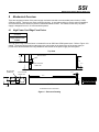
Mechanical Overview
There are two physical sizes of the power supply enclosure intended to accommodate power levels of 125W,
250W and 350W. There are two output connector designs. A card edge solution to provide ease of installation
and removal and a wire harness to provide a traditional cabled solution. The chassis for the entry 1U power
supply is designed for use in 1U rack mounted systems.
4.1
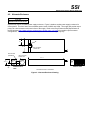
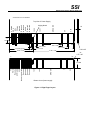
High Power Card Edge Form Factor
STATUS
Large Power Form
Factor
The high power edge card form factor is intended for use at 250W and 350W power levels. Refer to Figure 1 for
details. The supply will provide its output power via a card edge on the interior face of the power supply to
provide users and manufacturers easy installation and removal of the power supply into the system.
Top View
IEC Connector
53.0 +/- 0.2
80.92 +0/-0.05
106.0
+/- 0.2
12.54
IEC Connector
Center Line
Bi-Color LED
(PWR/Fail)
40.0 +0.2/-0.5
Fan
IEC Connector
Center Line
AC I/P
8.5 +/-0.3
300.0 +/-0.2
5.0 +/-0.3
Fan
Exterior Face View
+/-0.3
Side View
16.4 +/- 0.2
All dimensions are in millimeters.
Figure 1: Enclosure Drawing
62
32
1
31
Interior Face View
SSI
EPS1U Power Supply Design Guide, V1.1
4.2
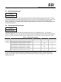
Alternate Enclosure
STATUS
Small Power Form Factor
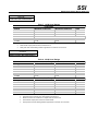
Systems may require a smaller power supply enclosure. Figure 2 details a smaller power supply enclosure for
such systems. This form factor accommodates power levels of 250W and 125W. The supply will provide output
power via a wire harness out the interior face of the supply. Refer to the Entry Electronics Bay Specification at
the SSI web site (http://www.ssiforum.org/docs/entry_elecbay_spec_v2_0.pdf) for possible output connector
configurations. Due to different system board layouts the wire harness length may vary.
53.0 +/- 0.2
IEC Connector
106.0 +/- 0.2
IEC Connector
Center Line
Bi-Color LED
(PWR/Fail)
40.0 +0.2/-0.5
16.4 +/- 0.2
Fan
IEC Connector
Center Line
AC I/P
215.0 +/-0.2
Fan
Exterior Face
face
Interior Face
All dimensions are in millimeters.
Figure 2: Alternate Enclosure Drawing
SSI
EPS1U Power Supply Design Guide, V1.1
4.3
Airflow Requirements
STATUS
Recommended
The power supply shall have a two-speed fan(s) and provide cooling to both the supply and the system. During
low-speed fan operation, the power supply shall not exceed a noise level of 38 dBA measured at one meter on all
faces. At low fan speed, the power supply shall provide a minimum of 6 CFM of airflow with 0.003 inH2O of
system backpressure. At high fan speed, the power supply shall provide a minimum of 10 CFM with 0.006 inH2O
of system backpressure.
4.4
Temperature Requirements
STATUS
Recommended
The power supply shall operate within all specified limits over the Top temperature range. The average air
temperature difference (∆Tps ) from the inlet to the outlet of the power supply shall not exceed the values shown in
Table 2. All airflow shall pass through the power supply and not over the exterior surfaces of the power supply.
Item
Table 2: Thermal Requirements
Description
MIN
Top
Operating temperature range.
∆Tps
Temperature rise from inlet air to outlet air of power supply.
125 W output power, 10 CFM, Sea level, 25 °C inlet air.
125 W output power, 6 CFM, Sea level, 25 °C inlet air.
Temperature rise from inlet air to outlet air of power supply.
250 W output power, 10 CFM, Sea level, 25 °C inlet air.
250 W output power, 6 CFM, Sea level, 25 °C inlet air.
350 W output power, 10 CFM, Sea level, 25 °C inlet air.
350 W output power, 6 CFM, Sea level, 25 °C inlet air.
Non-operating temperature range.
Tnon-op
0
-40
MAX
Units
45
°C
15
25
°C
°C
20
30
30
40
70
°C
°C
°C
°C
°C
The power supply must meet UL enclosure requirements for temperature rise limits. All sides of the power
supply, with exception to the air exhaust side, must be classified as “Handle, knobs, grips, etc. held for short
periods of time only”.
SSI
EPS1U Power Supply Design Guide, V1.1
5
AC Input Requirements
STATUS
Required
The power supply shall incorporate universal power input with active power factor correction, which shall reduce
line harmonics in accordance with the EN61000-3-2 and JEIDA MITI standards.
5.1
AC Inlet Connector
STATUS
Required
The AC input connector shall be an IEC 320 C-14 power inlet. This inlet is rated for 15 A / 250 VAC.
5.2
AC Input Voltage Specification
STATUS
Required
The power supply must operate within all specified limits over the following input voltage range. Harmonic
distortion of up to 10% THD must not cause the power supply to go out of specified limits. The power supply shall
operate properly at 85 VAC input voltage to guarantee proper design margins.
Table 3: AC Input Rating
Parameter
MIN
Rated
MAX
Voltage (110)
Voltage (220)
Frequency
90 Vrms
180 Vrms
47 Hz
100-127 Vrms
200-240 Vrms
140 Vrms
264 Vrms
63 Hz
1.
2.
3.
4.
5.3
MAX Input
Current
(125W)
1,3
2.4 Arms
2,3
1.2 Arms
MAX Input
Current
(250W)
1,3
4.2 Arms
2,3
2.1 Arms
MAX Input
Current
(350W)
1,3
5.9 Arms
2,3
3.0 Arms
MAX Rated Input
Current
(125W/250W/350W)
4
2.2 / 3.8 / 5.3Arms
4
1.1 / 1.9 / 2.7 Arms
Maximum input current at low input voltage range shall be measured at 90VAC. A 125W output load shall be applied to the
125W version, a 250 W output load shall be applied for the 250 W version and a 350 W output load shall be applied to the
350 W version.
Maximum input current at high input voltage range shall be measured at 180 VAC. A 125W output load shall be applied to
the 125W version, a 250 W output load shall be applied for the 250 W version and a 350 W output load shall be applied to the
350 W version.
This is not to be used for determining agency input current markings.
Maximum rated input current is measured at 100 VAC and 200 VAC.
Input Under Voltage
STATUS
Required
The power supply shall contain protection circuitry such that application of an input voltage below the minimum
specified in section 5.2 shall not cause damage to the power supply.
SSI
EPS1U Power Supply Design Guide, V1.1
5.4
Efficiency
STATUS
Required
The power supply shall have a minimum efficiency of 68% at maximum load and over the specified AC voltage.
There is no efficiency requirement for the 125W version.
5.5
AC Line Dropout
STATUS
Required
An AC line dropout is defined to be when the AC input drops to 0 VAC at any phase of the AC line for any length
of time. During an AC dropout of one cycle or less the power supply must meet dynamic voltage regulation
requirements over the rated load. An AC line dropout of one cycle or less shall not cause any tripping of control
signals or protection circuits. If the AC dropout lasts longer than one cycle, the power supply should recover and
meet all turn on requirements. The power supply must meet the AC dropout requirement over rated AC voltages,
frequencies, and output loading conditions. Any dropout of the AC line shall not cause damage to the power
supply.
5.6
AC Line Fuse
STATUS
Required
The power supply shall incorporate one input fuse on the LINE side for input over current protection to prevent
damage to the power supply and meet product safety requirements. Fuses should be slow blow type or
equivalent to prevent nuisance trips. AC inrush current shall not cause the AC line fuse to blow under any
conditions. All protection circuits in the power supply shall not cause the AC fuse to blow unless a component in
the power supply has failed. This includes DC output load short conditions.
STATUS
Optional
Some system applications may require a second input fuse in the NEUTRAL side of the AC input. In this case
two fuses would be required; one in the LINE side and one in the NEUTRAL side of the AC inlet to the power
supply.
5.7
AC Inrush
STATUS
Required
The power supply must meet inrush requirements for any rated AC voltage, during turn on at any phase of AC
voltage, during a single cycle AC dropout condition, during repetitive ON/OFF cycling of AC, and over the
specified temperature range (Top). The peak inrush current shall be less than the ratings of its critical components
(including input fuse, bulk rectifiers, and surge limiting device).
SSI
EPS1U Power Supply Design Guide, V1.1
STATUS
Recommended
An additional inrush current limit is recommended for some system applications that require multiple systems on a
single AC circuit. AC line inrush current shall not exceed 30 A peak for one-quarter of the AC cycle, after which,
the input current should be no more than the specified maximum input current from Table 3.
5.8
AC Line Transient Specification
STATUS
Recommended
AC line transient conditions shall be defined as “sag” and “surge” conditions. Sag conditions (also referred to as
“brownout” conditions) will be defined as the AC line voltage dropping below nominal voltage. Surge will be
defined as the AC line voltage rising above nominal voltage.
The power supply shall meet the requirements under the following AC line sag and surge conditions.
Duration
Sag
Table 4: AC Line Sag Transient Performance
Operating AC Voltage
Line Frequency Performance Criteria
Continuous
0 to 1 AC cycle
> 1 AC cycle
10%
100%
>10%
Nominal AC Voltage ranges
Nominal AC Voltage ranges
Nominal AC Voltage ranges
Duration
Surge
Table 5: AC Line Surge Transient Performance
Operating AC Voltage
Line Frequency Performance Criteria
Continuous
0 to ½ AC cycle
10%
30%
5.9
Nominal AC Voltages
Mid-point of nominal AC
Voltages
50/60 Hz
50/60 Hz
50/60 Hz
50/60 Hz
50/60 Hz
No loss of function or performance
No loss of function or performance
Loss of function acceptable, selfrecoverable
No loss of function or performance
No loss of function or performance
AC Line Fast Transient Specification
STATUS
Recommended
The power supply shall meet the EN61000-4-5 directive and any additional requirements in IEC1000-4-5:1995
and the Level 3 requirements for surge-withstand capability, with the following conditions and exceptions:
•
These input transients must not cause any out-of-regulation conditions, such as overshoot and
undershoot, nor must it cause any nuisance trips of any of the power supply protection circuits.
•
The surge-withstand test must not produce damage to the power supply.
•
The supply must meet surge-withstand test conditions under maximum and minimum DC-output load
conditions.
SSI
EPS1U Power Supply Design Guide, V1.1
6
DC Output Specification
6.1
Connector
STATUS
Required
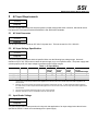
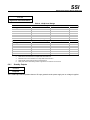
The power supply uses a blind mating type connector with edge fingers (see Figure 1) to connect the power
supply’s output voltages and signals to a connector located in the system. The card edge pin assignments are
listed in Table 6. Figure 3 shows the card edge layout for the power supply. The connector located in the system
is an AMP 1364999-1 or equivalent.
#
Signals that can be defined as low true or high true use the following convention: signal = low true. Reserved
pins are reserved for future use.
Table 6: Edge Finger Pinout
Description
-12V
PWOK
Reserved
ACWarning
5VSB
Removed pin
Reserved
Reserved
Reserved
Reserved
12V2
12V2
12V2
12V1
12V1
12V1
Ground
Ground
Ground
Ground
Ground
Ground
Ground
Ground
Ground
5V
5V
5V
3.3V
3.3V
3.3V
Pin#
Pin#
1
62
2
61
3
60
4
59
5
58
6
57
7
56
8
55
9
54
10
53
11
52
Keying notch between positions 11 and 12
12
51
13
50
14
49
15
48
16
47
17
46
18
45
19
44
20
43
21
42
22
41
23
40
24
39
25
38
26
37
27
36
28
35
29
34
30
33
31
32
Description
PSON#
SDA
SCL
PSAlert#
ReturnS
Reserved
Reserved
3.3VS
Reserved
Reserved
12V2
12V2
12V2
12V1
12V1
12V1
Ground
Ground
Ground
Ground
Ground
Ground
Ground
Ground
Ground
5V
5V
5V
3.3V
3.3V
3.3V
SSI
EPS1U Power Supply Design Guide, V1.1
All dimensions are in millimeters.
3.3V
1.6
5V
12V1
GROUND
Keying Notch
12V2
Reserved
3.3VS
Reserved
Reserved
PSON#
SDA
SCL
PSAlert#
ReturnS
Reserved
Top View of Power Supply
7.62 MIN
62
1.27 +/-0.05
21.59 +/-0.05
1.27
6.35 +/-0.05
6.35 +/-0.05
9 spaces @ 2.54
6.35 +/-0.05
1.07 +/-0.05
29.03 +/-0.05
32
6.35 +/-0.05
0.38 x 45
51.89 +/-0.05
2x
1.57 x 45
1
31
2x
Bottom view of power supply
Figure 3: Edge Finger Layout
3.3V
5V
GROUND
12V1
12V2
Reserved
Reserved
Reserved
5VSB
Removed pin (NC)
Reserved
PWOK
Reserved
ACWarning
-12V
5.08 MIN
SSI
EPS1U Power Supply Design Guide, V1.1
6.2
Grounding
STATUS
Required
The ground of the pins of the power supply wire harness provides the power return path. The wire harness
ground pins shall be connected to safety ground (power supply enclosure).
6.3
Remote Sense
STATUS
Optional
The power supply may have remote sense return (ReturnS) to regulate out ground drops for all output voltages;
+3.3 V, +5 V, +12 V1, +12 V2, -12 V, and 5 VSB. The power supply may use remote sense (3.3VS) to regulate
out drops in the system for the +3.3 V output. The +5 V, +12 V1, +12 V2, –12 V, and 5 VSB outputs only use
remote sense referenced to the ReturnS signal. The remote sense input impedance to the power supply must be
greater than 200 Ω on 3.3 VS and ReturnS. This is the value of the resistor connecting the remote sense to the
output voltage internal to the power supply. Remote sense must be able to regulate out a minimum of 200 mV
drop on the +3.3 V output. The remote sense return (ReturnS) must be able to regulate out a minimum of 200 mV
drop in the power ground return. The current in any remote sense line shall be less than 5 mA to prevent voltage
sensing errors. The power supply must operate within specification over the full range of voltage drops from the
power supply’s output connector to the remote sense points.
6.4
Output Power/Currents
The following tables define three power and current ratings for a 125W, 250 W and a 350 W power supply. These
were selected to cover different types of systems and configurations. The 125W power level is targeted for use in
“today’s” low power server systems. The 250W power level is targeted for use in “today’s” higher power 1U
server systems. The 350W power level is directed at “tomorrow’s” higher power 1U server systems. The
combined output power of all outputs shall not exceed the rated output power. The tables show the load ranges
for each of the two power supply power levels. The power supply must meet both static and dynamic voltage
regulation requirements for the minimum loading conditions.
SSI
EPS1U Power Supply Design Guide, V1.1
STATUS
Low Power Recommendation
Voltage
Table 7: 125 W Load Ratings
Load Range
Minimum Continuous
Maximum Continuous
+3.3 V
+5 V
+12 V1
+12 V2
-12 V
0.5 A
0.5 A
0.25 A
Not used for 125W version.
0A
6A
12 A
3A
0.1 A
1.0 A
+5 VSB
1.
2.
3.
Peak
6A
0.2 A
Maximum continuous total DC output power should not exceed 125 W.
Peak total DC output power should not exceed 161 W.
Peak power and current loading shall be supported for a minimum of 12 seconds.
STATUS
Medium Power Recommendation
Voltage
Table 8: 250 W Load Ratings
Load Range 1
Minimum Continuous
Maximum Continuous
+3.3 V
+5 V
+12 V1
+12 V2
-12 V
1.5 A
1.0 A
1.5 A
0.5 A
0A
+5 VSB
0.1 A
16 A
12 A
16 A
10 A
0.5 A
Voltage
2.0 A
Load Range 2
Minimum Continuous
Maximum Continuous
+3.3 V
+5 V
+12 V1
+12 V2
-12 V
+5 VSB
0.2 A
0.2 A
0.2 A
0.2 A
0A
0.1 A
1
2
3
4
5
5.0 A
5.0 A
8.0 A
2.0 A
0.5 A
2.0 A
Maximum continuous total DC output power should not exceed 250 W.
Peak load on the combined 12 V output shall not exceed 22 A.
Maximum load on the combined 12 V output shall not exceed 18 A.
Peak total DC output power should not exceed 300 W.
Peak power and current loading shall be supported for a minimum of 12 seconds.
Peak
See note 2
See note 2
Peak
4.0 A
SSI
EPS1U Power Supply Design Guide, V1.1
STATUS
High Power Recommendation
Voltage
Table 9: 350 W Load Ratings
Load Range 1
Minimum Continuous
Maximum Continuous
+3.3 V
+5 V
+12 V1
+12 V2
-12 V
+5 VSB
1.5 A
1.0 A
1.5 A
1.5 A
0A
0.1 A
Voltage
Load Range 2
Minimum Continuous
Maximum Continuous
+3.3 V
+5 V
+12 V1
+12 V2
-12 V
+5 VSB
0.2 A
0.2 A
0.2 A
0.2 A
0A
0.1 A
1.
2.
3.
4.
5.
6.4.1
16 A
12 A
16 A
16 A
0.5 A
2.0 A
5.0 A
5.0 A
8.0 A
2.0 A
0.5 A
2.0 A
Peak
See note 2
See note 2
Peak
5.0 A
Maximum continuous total DC output power should not exceed 350 W.
Peak load on the combined 12 V output shall not exceed 32 A.
Maximum load on the combined 12 V output shall not exceed 28 A.
Peak total DC output power should not exceed 400 W.
Peak power and current loading shall be supported for a minimum of 12 seconds.
Standby Outputs
STATUS
Required
The 5 VSB output shall be present when an AC input greater than the power supply turn on voltage is applied.
SSI
EPS1U Power Supply Design Guide, V1.1
6.5
Voltage Regulation
STATUS
Required
The power supply output voltages must stay within the following voltage limits when operating at steady state and
dynamic loading conditions. These limits include the peak-peak ripple/noise specified in Section 6.8. All outputs
are measured with reference to the return remote sense (ReturnS) signal. The 5 V, 12 V1, 12 V2, –12 V and 5
VSB outputs are measured at the power supply connectors referenced to ReturnS. The +3.3 V is measured at its
remote sense signal (3.3 VS) located at the signal connector.
Table 10: Voltage Regulation Limits
NOM
MAX
Units
Parameter
MIN
+3.3 V
+5 V
+12 V1
+12 V2
+3.20
+4.80
+11.52
+11.52
+3.30
+5.00
+12.00
+12.00
+3.46
+5.25
+12.60
+12.60
Vrms
Vrms
Vrms
Vrms
+5/-3%
+5/-4%
+5/-4%
+5/-4%
Tolerance
-12 V
+5 VSB
-11.40
+4.85
-12.20
+5.00
-13.08
+5.25
Vrms
Vrms
+9/-5%
+5/-4%
STATUS
Optional
Some system applications may require tighter regulation limits on the +5 V output. The optional regulation limits
are shown below.
6.6
Parameter
Table 11: Optional +5V Regulation Limits
MIN
NOM
MAX
Units
Tolerance
+5 V
+4.85
+5.00
+5.25
Vrms
+5/-3%
Dynamic Loading
STATUS
Required
The output voltages shall remain within the limits specified in Table 10 for the step loading and within the limits
specified in Table 12 for the capacitive loading. The load transient repetition rate shall be tested between 50 Hz
and 5 kHz at duty cycles ranging from 10%-90%. The load transient repetition rate is only a test specification.
The ∆ step load may occur anywhere within the MIN load to the MAX load shown in Table 8 and Table 9.
Output
+3.3 V
+5 V
12 V1+(12 V2)
+5 VSB
Table 12: Transient Load Requirements
∆ Step Load Size Load Slew Rate Capacitive Load
30% of max load
30% of max load
65% of max load
25% of max load
0.5 A/µs
0.5 A/µs
0.5 A/µs
0.5 A/µs
100 µF
100 µF
1,000 µF
1 µF
SSI
EPS1U Power Supply Design Guide, V1.1
6.7
Capacitive Loading
STATUS
Required
The power supply shall be stable and meet all requirements with the following capacitive loading ranges.
Output
6.8
Table 13: Capacitive Loading Conditions
MIN
MAX
Units
+3.3 V
+5 V
+12 V
10
10
10
6,800
4,700
11,000
µF
µF
µF
-12 V
+5 VSB
1
1
350
350
µF
µF
Ripple / Noise
STATUS
Required
The maximum allowed ripple/noise output of the power supply is defined in Table 14 below. This is measured
over a bandwidth of 0 Hz to 20 MHz at the power supply output connectors. A 10 µF tantalum capacitor in
parallel with a 0.1 µF ceramic capacitor are placed at the point of measurement.
Table 14: Ripple and Noise
+12 V
-12 V
+3.3 V
+5 V
50 mVp-p
50 mVp-p
120 mVp-p
120 mVp-p
+5 VSB
50 mVp-p
SSI
EPS1U Power Supply Design Guide, V1.1
6.9
Timing Requirements
STATUS
Required
These are the timing requirements for the power supply operation. The output voltages must rise from 10% to
within regulation limits (Tvout_rise) within 5 to 70 ms. The +3.3 V, +5 V and +12 V output voltages should start to
rise at about the same time. All outputs must rise monotonically. The +5 V output needs to be greater than the
+3.3 V output during any point of the voltage rise. The +5 V output must never be greater than the +3.3V output
by more than 2.25 V. Each output voltage shall reach regulation within 50 ms (Tvout_on) of each other during turn
on of the power supply. Each output voltage shall fall out of regulation within 400 ms (Tvout_off) of each other
during turn off. Figure 4 and Figure 5 show the turn ON and turn OFF timing requirements. In Figure 5 the timing
is shown with both AC and PSON# controlling the ON/OFF of the power supply.
Table 15: Output Voltage Timing
MIN
Item
Description
Tvout_rise
Output voltage rise time from each main output.
Tvout_on
All main outputs must be within regulation of each
other within this time.
All main outputs must leave regulation within this
time.
T vout_off
5
Vout
V1
10%
Vout
V2
V3
V4
Tvout_rise
Tvout_off
Tvout_on
Figure 4: Output Voltage Timing
MAX
Units
70
ms
50
ms
400
ms
SSI
EPS1U Power Supply Design Guide, V1.1
Table 16: Turn On/Off Timing
MIN
Item
Description
Tsb_on_delay
Delay from AC being applied to 5 VSB being
within regulation.
Delay from AC being applied to all output
voltages being within regulation.
Time all output voltages stay within regulation
after loss of AC.
Delay from loss of AC to deassertion of PWOK
T ac_on_delay
Tvout_holdup
Tpwok_holdup
Tpson_on_delay
Delay from PSON# active to output voltages
within regulation limits.
Delay from PSON# deactive to PWOK being
deasserted.
Delay from output voltages within regulation
limits to PWOK asserted at turn on.
Delay from PWOK deasserted to output
voltages (3.3 V, 5 V, 12 V, -12 V) dropping out
of regulation limits.
Duration of PWOK being in the deasserted state
during an off/on cycle using AC or the PSON#
signal.
Delay from 5 VSB being in regulation to O/Ps
being in regulation at AC turn on.
T pson_pwok
Tpwok_on
T pwok_off
Tpwok_low
Tsb_vout
MAX
Units
1500
ms
2500
ms
18
ms
17
ms
5
100
400
ms
50
ms
1000
ms
1
ms
100
ms
50
1000
ms
STATUS
Recommended
Item
Description
MIN
Tvout_holdup
Time all output voltages stay within regulation
after loss of AC.
Delay from loss of AC to deassertion of PWOK.
Time 5VSB output voltage stays within regulation
after loss of AC.
21
ms
20
70
ms
ms
Tpwok_holdup
Tsb_holdup
MAX
UNITS
SSI
EPS1U Power Supply Design Guide, V1.1
AC Input
Tvout_holdup
Vout
Tpwok_low
TAC_on_delay
Tsb_on_delay
Tpwok_on
PWOK
5VSB
Tpwok_off
Tsb_on_delay
Tpwok_on
Tpson_pwok
Tpwok_holdup
Tsb_holdup
Tsb_vout
Tpson_on_delay
PSON#
AC turn on/off cycle
Tpwok_off
PSON turn on/off cycle
Figure 5: Turn On/Off Timing (Signal Power Supply)
SSI
EPS1U Power Supply Design Guide, V1.1
7
Protection Circuits
STATUS
Required
Protection circuits inside the power supply shall cause only the power supply’s main outputs to shutdown. If the
#
power supply latches off due to a protection circuit tripping, an AC cycle OFF for 15 seconds and a PSON cycle
HIGH for 1 second shall be able to reset the power supply.
7.1
Current Limit
STATUS
Required
The power supply shall have current limit to prevent the +3.3 V, +5 V, and +12 V outputs from exceeding the
values shown in Table 17. If the current limits are exceeded, the power supply shall shutdown and latch off. The
#
latch will be cleared by toggling the PSON signal or by an AC power interruption. The power supply shall not be
damaged from repeated power cycling in this condition. –12 V and 5 VSB shall be protected under over current
or shorted conditions so that no damage can occur to the power supply. All outputs shall be protected so that no
damage occurs to the power supply under a shorted output condition.
Table 17: Over Current Protection
Over Current Limit (Iout limit)
Voltage
+3.3 V
+5 V
+12 V
7.2
110% minimum; 150% maximum
110% minimum; 150% maximum
110% minimum; 150% maximum
240VA Protection
STATUS
Recommended
System designs may require user access to energized areas of the system. In these cases the power supply may
be required to meet regulatory 240VA limits for any power rail. Since the +12V rail combined power exceeds
240VA it must be divided into separate channels to meet this requirement. Each separate rail needs to be limited
to less than 20A for each +12V rail. The separate +12V rails do not necessarily need to be independently
regulated outputs. They can share a common power conversion stage. The +12V rail is divided into two rails for
the 250W and 350W power levels. +12V1 is dedicated for providing power to the input of the processor voltage
regulator(s). The +12V2 rail is used to power the rest of the main board +12V power needs and peripherals
devices.
Table 18: Over Current Protection
Voltage
Over Current Limit (Iout limit)
+3.3 V
+5 V
+12V1
+12V2
110% minimum; 150% maximum
110% minimum; 150% maximum
18A minimum; 20A maximum
18A minimum; 20A maximum
SSI
EPS1U Power Supply Design Guide, V1.1
7.3
Over Voltage Protection
STATUS
Required
The power supply over voltage protection shall be locally sensed. The power supply shall shutdown and latch off
#
after an over voltage condition occurs. This latch shall be cleared by toggling the PSON signal or by an AC
power interruption. Table 19 contains the over voltage limits. The values are measured at the output of the
power supply’s connectors. The voltage shall never exceed the maximum levels when measured at the power
pins of the power supply connector during any single point of fail. The voltage shall never trip any lower than the
minimum levels when measured at the power pins of the power supply connector.
Output Voltage
Table 19: Over Voltage Limits
MIN (V)
MAX (V)
3.9
5.7
13.3
-13.3
5.7
4.5
6.5
14.5
-14.5
6.5
+3.3 V
+5 V
+12 V1, 2
-12 V
+5 VSB
7.4
Over Temperature Protection
STATUS
Recommended
The power supply will be protected against over temperature conditions caused by loss of fan cooling or
excessive ambient temperature. In an OTP condition the PSU will shutdown. When the power supply
temperature drops to within specified limits, the power supply shall restore power automatically. The OTP circuit
must have built in hysteresis such that the power supply will not oscillate on and off due to temperature recovering
condition. The OTP trip level shall have a minimum of 4 °C of ambient temperature hysteresis.
SSI
EPS1U Power Supply Design Guide, V1.1
8
Control and Indicator Functions
The following sections define the input and output signals from the power supply.
Signals that can be defined as low true use the following convention:
#
signal = low true
8.1
PSON#
STATUS
Required
#
#
The PSON signal is required to remotely turn on/off the power supply. PSON is an active low signal that turns
on the +3.3 V, +5 V, +12 V, and –12 V power rails. When this signal is not pulled low by the system, or left open,
the outputs (except the +5 VSB and Vbias) turn off. This signal is pulled to a standby voltage by a pull-up resistor
internal to the power supply. Refer to Figure 5 for the timing diagram.
#
Table 20: PSON Signal Characteristic
Accepts an open collector/drain input from the system.
Pull-up to VSB located in power supply.
ON
Signal Type
#
PSON = Low
#
OFF
PSON = Open or High
MIN
Logic level low (power supply ON)
Logic level high (power supply OFF)
MAX
0V
1.0 V
2.0 V
5.25 V
4 mA
Source current, Vpson = low
5 ms
Power up delay: Tpson_on_delay
400 ms
50 ms
PWOK delay: Tpson_pwok
Hysteresis ≥ 0.3V and/or other de-bounce method
Disabled
≤ 1.0 V
PS is
enabled
≥ 2.0 V
PS is
disabled
Enabled
0V
1.0V
2.0V
5.25V
Figure 6: PSON# Signal Characteristics
SSI
EPS1U Power Supply Design Guide, V1.1
8.2
PWOK (Power OK)
STATUS
Required
PWOK is a power OK signal and will be pulled HIGH by the power supply to indicate that all the outputs are within
the regulation limits of the power supply. When any output voltage falls below regulation limits or when AC power
has been removed for a time sufficiently long so that power supply operation is no longer guaranteed, PWOK will
be de-asserted to a LOW state. See Figure 5 for a representation of the timing characteristics of PWOK. The
start of the PWOK delay time shall be inhibited as long as any power supply output is in current limit.
Table 21: PWOK Signal Characteristics
PWOK = High
Open collector/drain output from power supply. Pull-up
to VSB located in power supply.
Power OK
PWOK = Low
Power not OK
Signal Type
MIN
Logic level low voltage, Isink=4 mA
Logic level high voltage, Isource=200 µA
Sink current, PWOK = low
0V
0.4 V
2.4 V
5.25 V
4 mA
2 mA
Source current, PWOK = high
PWOK delay: T pwok_on
200 ms
1000 ms
100 µs
PWOK rise and fall time
Power down delay: T pwok_off
MAX
1 ms
SSI
EPS1U Power Supply Design Guide, V1.1
8.3
ACWarning
STATUS
Optional
This is an output signal from the power supply which provides a warning to the system that the power supply has
lost its AC input. This signal also provides a signal to synchronize the turn on of multiple power supplies. At turn
on, this signal is pulled LOW when the supply’s internal bulk voltage has reached a level that allows it to turn on.
At turn off ACWarning goes HIGH when the internal bulk voltage drops low enough. The characteristics of the
ACWarning signal is shown in Table 22: ACWarning Signal Characteristics. Refer to Figure 5 for timing diagram.
Table 22: ACWarning Signal Characteristics
Open collector/drain output from power supply. Pullup to VSB located in system.
ACWarning = Low
Input voltage within operating range and power
supply is ready to turn on.
ACWarning = High
Input voltage is less than the operating range and the
power supply is turning off.
MIN
MAX
Logic level low voltage, Isink=4mA
0V
0.4V
5.25V
Logic level high voltage, Isink=50µA
Sink current, ACWarning = low
4mA
Sink current, ACWarning = high
50µA
ACWarning Delay: Tacwarning_delay
8msec
ACWarning rise and fall time
100µsec
Power supply turn on voltage
75VAC
85VAC
Signal Type
SSI
EPS1U Power Supply Design Guide, V1.1
8.4
Field Replacement Unit (FRU) Signals
STATUS
Optional
Two pins will be allocated for the FRU information on the power supply connector. One pin is the Serial Clock
(SCL). The second pin is used for Serial Data (SDA). Both pins are bi-directional and are used to form a serial
bus. The FRU circuits inside the power supply must be powered off of 5 VSB output and grounded to ReturnS
(remote sense return). The Write Control (or Write protect) pin should be tied to ReturnS inside the power supply
so that information can be written to the EEPROM.
8.4.1
FRU Data
FRU data shall be stored starting in address location 8000h through 80FFh. The FRU data format shall be
compliant with the IPMI specifications. The current version of these specifications is available at
http:\\developer.intel.com/design/servers/ipmi/spec.htm.
8.4.2
FRU Data Format
The information to be contained in the FRU device is shown in the following table.
Table 23: FRU Device Information
Area Type
Description
Common Header
Internal Use Area
Chassis Info Area
Board Info Area
As defined by the FRU document
Not required, do not reserve
Not applicable, do not reserve
Not applicable, do not reserve
8.4.2.1
Product Info Area
As defined by the IPMI FRU document. Product information shall be defined as follows:
Field Name
Manufacturer Name
Product Name
Product part/model
number
Product Version
Product Serial Number
Asset Tag
FRU File ID
PAD Bytes
Table 24: FRU Device Product Information Area
Field Description
{Formal name of manufacturer}
{Manufacturer’s model number}
Customer part number
Customer current revision
{Defined at time of manufacture}
{Not used, code is zero length byte}
{Not required}
{Added as necessary to allow for 8-byte offset to next area}
SSI
EPS1U Power Supply Design Guide, V1.1
8.4.2.2
MultiRecord Area
As defined by the IPMI FRU document. The following record types shall be used on this power supply:
•
Power Supply Information (Record Type 0x00)
•
DC Output (Record Type 0x01)
•
No other record types are required for the power supply.
MultiRecord information shall be defined as follows:
Field Name (PS Info)
Table 25: FRU Device MultiRecord Area
Field Information Definition
Overall Capacity (W)
Peak VA
Inrush current (A)
Inrush interval (ms)
Low end input voltage
range 1
350 {Low power versions would be 250 or 125}
400 {Low power versions would be 300 or 161}
30
5
90
High end input voltage
range 1
140
Low end input voltage
range 2
High end input voltage
range 2
A/C dropout tol. (ms)
Binary flags
Peak Wattage
Combined wattage
180
Predictive fail tach
support
Field Name (Output)
Output Information
All other output fields
264
20
Set for: Not Hot Swap support, Auto-switch, and PFC
Set for: 12 s, 400 W {Low power versions would be 300W or 161W}
Set for 5 V & 3.3 V combined wattage of 113 W {Low power versions would be 113W
or 80}
Not supported, 00h value
Field Description: Six outputs are to be defined from #1 to #6, as follows: +3.3 V, +5
V, +12 V1, +12V2, -12 V, and +5 VSB.
Set for: Standby on +5 VSB, No Standby on all others.
Format per IPMI specification, using parameters in the EPS1U specification.
SSI
EPS1U Power Supply Design Guide, V1.1
8.5
LED Indicator
STATUS
Required
There will be a single GREEN LED to indicate power supply status. When AC is applied to the PSU and standby
voltages are available the LED shall BLINK GREEN. The LED shall turn ON GREEN to indicate that all the power
outputs are available. Refer to Table 26 for conditions of the LED.
Table 26: LED Indicators
Power Supply Condition
Power Supply LED
No AC power to PSU or PSU failure
AC present / Only Standby Output ON
Power supply DC outputs ON and OK
OFF
BLINK GREEN
GREEN
The LED shall be visible on the power supply’s exterior face. The LED location shall meet ESD requirements.
LED shall be securely mounted in such a way that incidental pressure on the LED shall not cause it to become
displaced.
9
MTBF
STATUS
Recommended
The power supply shall have a minimum MTBF at continuous operation of 1) 100,000 hours at 100% load and
45° C, as calculated by Bellcore RPP, or 2) 250,000 hours demonstrated at 100% load and 45° C.
SSI
EPS1U Power Supply Design Guide, V1.1
10 Agency Requirements
STATUS
Recommended
The power supply must comply with all regulatory requirements for its intended geographical market. Depending
on the chosen market, regulatory requirements may vary. Although a power supply can be designed for
worldwide compliance, there may be cost factors that drive different versions of supplies for different
geographically targeted markets.
This specification requires that the power supply meet all regulatory requirements for the intended market at the
time of manufacturing. Typically this includes:
•
UL
•
CSA
•
A Nordic CENELEC
•
TUV
•
VDE
•
CISPR Class B
•
FCC Class B
The power supply, when installed in the system, shall meet immunity requirements specified in EN55024.
Specific tests are to be EN61000-4-2 ,-3, -4, -5, -6, -8, and -11. The power supply must maintain normal
performance within specified limits. This testing must be completed by the system EMI engineer. Conformance
must be designated with the European Union CE Marking. Specific immunity level requirements are left to
customer requirements.