1
TSP-10G3A1EER
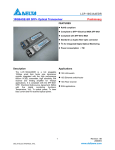
10GBASE-SR XFP Optical Transceiver
FEATURES
RoHS compliant
850nm Vertical Cavity Surface Emitting Laser
(VCSEL) light source
Standard LC duplex fiber-optic connector
Compliant with XFP MSA
I2C for integrated Digital Optical Monitoring
Power consumption <1.37 W
User friendly Plug-and-play style "Hot Swap"
Small footprint which enables high board
density
XFI high speed I/O electrical interface
Integrated signal conditioner to extend
200mm FR4 PCB trace signaling
Description
Application
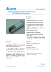
The TSP-10G3A1EER is a hot pluggable
10Gbps small form factor transceiver module
integrated with the high performance 850nm
VCSEL transmitter, high sensitivity PIN receiver
and signal conditioner for 10Gbps applications.
10G LAN switch
10G Ethernet switch/router
10G Fiber channel
SAN applications
It is compliant with the INF-8077i XFP
Multi-source Agreement (MSA).
The TSP-10G3A1EER is designed to be
compliant with INF-8077i XFP Multi-source
Agreement (MSA) with five digital monitoring
functions: Temperature, Vcc, Tx optical power,
TX laser bias current and RX received optical
power.
1
DELTA ELECTRONICS, INC.
Revision: S3
04/10/2007
www.deltaww.com
TSP-10G3A1EER
1. Absolute Maximum Ratings
Parameter
Symbol
Min
Storage Temperature
Storage Ambient Humidity
+5V Power Supply
+3.3V Power Supply
TS
HA
VCC5
VCC3
-40
5
0
0
Typ
Max
Units
Notes
85
90
6.0
3.6
°C
%
V
V
Max
Units
70
°C
85
3.465
5.25
350
30
1.37
%
V
V
mA
mA
W
[1]
3.3
5
270
10
150
500
1000
mVp-p
[2,3]
500
650
800
mVp-p
[4]
2. Recommended Operating Conditions
Parameter
Operating Ambient
Temperature
Ambient Humidity
+3.3V Power Supply
+5V Power Supply
+3.3V Supply Current
+5V Supply Current
Total Power Dissipation
Differential TX Data Input
Differential RX Data Output
Symbol
Min
TA
0
HA
VCC3
VCC5
IVCC3
IVCC5
PD
5
3.135
4.75
TD+ - TD+
-
RD - RD
Typ
Notes
Notes:
1. Non-condensing
2. The data rate of input data is 10.3125Gb/s
3. Input voltage swing (differential) measured peak-to-peak
4. Output voltage swing (differential) measured peak-to-peak
ASIC / SerDes
XFP
10Gbps XFI electrical signal
XFP
10Gbps optical signal
ASIC / SerDes
10Gbps XFI electrical signal
Application Block Diagram
2
DELTA ELECTRONICS, INC.
Revision: S3
04/10/2007
www.deltaww.com
TSP-10G3A1EER
3. Optical Transmitter Characteristics (TA=0 ºC to 70 ºC)
Parameter
Symbol
Min
Typ
Max
Units
Data Rate
R
10.3125
Signaling speed variation from
±100
nominal
Average Output Power
Pavg
-5
-1.8
Wavelength
840
860
λ
Spectral Width RMS
0.45
Transmitter OFF Output Power
Poff
-30
Extinction Ratio
ER
3.7
Optical Modulaion Amplitude
OMA Compliant with Minimum OMA relation table
RIN12OMA
Relative Intensity Noise
-128
ORLT
Optical Return Loss Tolerance
12
Transmitter eye mask definition
{X1, X2, X3, Y1, Y2, Y3}
Notes
Gb/s
ppm
dBm
nm
nm
dBm
dB
dBm
dB/Hz
dB
{0.25, 0.40, 0.45, 0.25, 0.28, 0.40}
Transmitter eye mask definition
Minimum optical modulation amplitude (dBm) relation table
Center
Wavelength
(nm)
840 to 842
842 to 844
844 to 846
846 to 848
848 to 850
850 to 852
852 to 854
854 to 856
856 to 858
858 to 860
RMS Specrtal width (nm)
Up to 0.05 to 0.1 to 0.15 to 0.2 to 0.25 to 0.3 to 0.35 to 0.4 to
0.05
0.1
0.15
0.2
0.25
0.3
0.35
0.4
0.45
-4.2
-4.2
-4.2
-4.3
-4.3
-4.3
-4.3
-4.3
-4.3
-4.3
-4.2
-4.2
-4.2
-4.2
-4.2
-4.2
-4.2
-4.3
-4.3
-4.3
-4.1
-4.2
-4.2
-4.2
-4.2
-4.2
-4.2
-4.2
-4.2
-4.2
-4.1
-4.1
-4.1
-4.1
-4.1
-4.1
-4.1
-4.1
-4.1
-4.2
3
DELTA ELECTRONICS, INC.
-3.9
-3.9
-4.0
-4.0
-4.0
-4.0
-4.0
-4.0
-4.0
-4.1
-3.8
-3.8
-3.8
-3.8
-3.8
-3.8
-3.9
-3.9
-3.9
-3.9
-3.5
-3.6
-3.6
-3.6
-3.6
-3.6
-3.7
-3.7
-3.7
-3.7
-3.2
-3.3
-3.3
-3.3
-3.3
-3.4
-3.4
-3.4
-3.5
-3.5
-2.8
-2.9
-2.9
-2.9
-3.0
-3.0
-3.1
-3.1
-3.1
-3.2
Revision: S3
04/10/2007
www.deltaww.com
TSP-10G3A1EER
Triple tradeoff curve
4. Optical Receive Characteristics (TA=0 ºC to 70 ºC)
Parameter
Signaling speed (nominal)
Signaling speed variation from
nominal
Center Wavelength
Overload
Receiver sensitivity in OMA
LOS De-assert
LOS Assert
LOS Hysteresis
Symbol
Min
Ts
λ
PO
RSO
LOSD
LOSA
LOSD –LOSA
Typ
Max
10.3125
840
Notes
Gb/s
±100
ppm
860
-1
-11.1
-13
nm
dBm
dBm
dBm
dBm
[2]
-12
dB
dB
[3]
-7.5
dBm
-30
0.5
Receiver Reflectance
Stressed Receive sensitivity
OMA
Units
[1]
Notes:
1.
2.
3.
−12
Measured by reference TX with 4.75dB extinction ratio at 10 BER
When LOS asserted, the data output is Low-level (fixed)
When the terminal is viewed from the optical path, the reflection toward the optical path of the optical
signal with a central wavelength of 840nm to 860nm transmitted to terminal.
4
DELTA ELECTRONICS, INC.
Revision: S3
04/10/2007
www.deltaww.com
TSP-10G3A1EER
5. XFI Module Receiver Output Jitter Specifications at C’
Parameter – C’
Symbol
Deterministic Jitter
Total Jitter
DJ
TJ
X1
X2
Y1
Y2
Eye Mask
Min
Typ
Max
Units
Notes
0.18
0.34
0.17
0.42
UI (p-p)
UI (p-p)
UI
UI
mV
mV
[1]
[1]
170
425
Notes:
1. Includes jitter transferred from the optical receiver during any valid operational input condition.
XFI Module Receiver Differential Output Compliance Mask
XFI Termination and AC Coupling
5
DELTA ELECTRONICS, INC.
Revision: S3
04/10/2007
www.deltaww.com
TSP-10G3A1EER
6. Pin Description
XFP Host Board Connector Pad Layout (Top View)
Recommended Host Board Supply Filtering Network
6
DELTA ELECTRONICS, INC.
Revision: S3
04/10/2007
www.deltaww.com
TSP-10G3A1EER
Module Electrical Pin Function Definition
Pin
Logic
Symbol
Name/Description
1
GND
Module Ground
2
VEE5
Optional -5.2V Power Supply --Not Required
Note
[1]
3
LVTTL-I
Mod_DeSel
Module De-select; When held low allows module to respond to
2-wire serial interface
4
LVTTL-O
Interrupt Bar
Interrupt Bar; Indicates presence of an important condition
which can be read over the 2-wire serial interface
5
LVTTL-I
TX_DIS
Transmitter Disable; Turns off transmitter laser output
6
VCC5
+5V Power Supply
7
GND
Module Ground
8
VCC3
+3.3V Power Supply
VCC3
+3.3V Power Supply
9
[2]
[1]
10
LVTTL-I/O
SCL
2-Wire Serial Interface Clock
[2]
11
LVTTL-I/O
SDA
2-Wire Serial Interface Data Line
[2]
12
LVTTL-O
Mod_Abs
Indicates Module is not present. Grounded in the Module
[2]
13
LVTTL-O
Mod_NR
Module Not Ready; Indicating Module Operational Fault
[2]
14
LVTTL-O
RX_LOS
Receiver Loss Of Signal Indicator
[2]
15
GND
Module Ground
[1]
16
GND
Module Ground
[1]
17
CML-O
RD-
Receiver Inverted Data Output
18
CML-O
RD+
Receiver Non-Inverted Data Output
19
GND
Module Ground
20
VCC2
+1.8V Power Supply --Not Required
21
LVTTL-I
[1]
Power down; When high, requires the module to limit power
P_Down/RST consumption to 1.5W or below. 2-Wire serial interface must be
functional in the low power mode.
22
VCC2
23
GND
24
PECL-I
RefCLK-
25
PECL-I
RefCLK+
+1.8V Power Supply --Not Required
Module Ground
[1]
Reference Clock Non-Inverted Input, AC coupled on the host board,
Not required
Reference Clock Inverted Input, AC coupled on the host board,
Not required
26
GND
Module Ground
[1]
27
GND
Module Ground
[1]
28
CML-I
TD-
Transmitter Inverted Data Input
29
CML-I
TD+
Transmitter Non-Inverted Data Input
GND
Module Ground
30
[1]
Notes:
1. Module ground pins Gnd are isolated from the module case and chassis ground within the module.
7
DELTA ELECTRONICS, INC.
Revision: S3
04/10/2007
www.deltaww.com
TSP-10G3A1EER
2. Shall be pulled up with 4.7K-10Kohms to a voltage between 3.15V and 3.45V on the host board.
7. Low Speed Electrical Hardware Pins
In addition to the 2-wire serial interface the XFP module has the following low speed pins for control and status:
• Mod_NR
• Mod_DeSel
• Interrupt
• TX_DIS
• Mod_ABS
• RX_Los
• P_Down/RST.
1 MOD_NR
The Mod_NR is an output pin that when High, indicates that the module has detected a condition that renders
transmitter and or receiver data invalid, shall consist of logical OR of the following signals:
• Transmit Signal Conditioner Loss of Lock
• Transmitter Laser Fault
• Receiver Signal Conditioner Loss of Lock
Other conditions deemed valuable to the detection of fault may be added to the Mod_NR.
The Mod_NR output pin is an open collector and must be pulled to Host_Vcc on the host board.
2 MOD_DESEL
The Mod_DeSel is an input pin. When held Low by the host, the module responds to 2-wire serial communication
commands. The Mod_DeSel allows the use of multiple XFP modules on a single 2-wire interface bus.
When the Mod_DeSel pin is “High”, the module shall not respond to or acknowledge any 2-wire interface
communication from the host. Mod_DeSel pin must be pulled to VCC3 in the module.
In order to avoid con.icts, the host system shall not attempt 2-wire interface communications within the Mod_DeSel
assert time after any XFP modules are deselected. Similarly, the host must wait at least for the period of the
Mod_DeSel deassert time before communicating with the newly selected module. The assertion and de-assertion
periods of different modules may overlap as long as the above timing requirements are met.
3 INTERRUPT
Interrupt is an output pin. When “Low”, indicates possible module operational fault or a status critical to the host
system. The Interrupt pin is an open collector output and must be pulled up to Host_Vcc the host board.
4 TX_DIS
TX_DIS is an input pin. When TX_DIS is asserted High, the XFP module transmitter output must be turned off. The
TX_DIS pin must be pulled up to VCC3 in the XFP module.
8
DELTA ELECTRONICS, INC.
Revision: S3
04/10/2007
www.deltaww.com
TSP-10G3A1EER
5 MOD_ABS
Mod_ABS is pulled up to Host_Vcc on the host board and grounded in the XFP module. Mod_ABS is then asserted
“High” when the XFP module is physically absent from a host slot.
6 RX_LOS
The RX_LOS when High indicates insuf.cient optical power for reliable signal reception. The RX_LOS pin is an open
collector output and must be pulled up to Host_Vcc on the host board.
7 P_DOWN/RST
This is a multifunction pin for module Power Down and Reset. The P_Down/RST pin must be pulled up to VCC3 in the
XFP module.
7.1 POWER DOWN FUNCTION
The P_Down pin, when held High by the host, places the module in the standby (Low Power) mode with a maximum
power dissipation of 1.5W.
This protects hosts which are not capable of cooling higher power modules which may be accidentally inserted.
The module’s 2-wire serial interface and all laser safety functions must be fully functional in this low power mode.
During P_Down, the module shall still support the completion of reset Interrupt, as well as maintain functionality of the
variable power supply as described in XFP MSA Revision 3.1 section 5.7.
7.2 RESET FUNCTION
The negative edge of P_Down/RST signal initiates a complete module reset.
7.3 MODULE BEHAVIOR DURING POWER DOWN AND RESET
During execution of a reset (t_init) or while held in Power Down mode, a module may be unable to determine the
correct value for Mod_NR and RX_LOS. These outputs as well as all interrupt related .ags, except completion of
Reset .ag, shall be disregarded by the host. When the module completes a Reset and is not in Power Down mode,
the module must represent the correct value of both signals on its outputs before posting a completion of reset
interrupt to the host (see XFP MSA Revision 3.1 Table 39, bit 0 register address 84).
At no time shall a module cause spurious assertion of the Interrupt pin.
When a host initially applies power to a module with the P_Down/RST signal asserted, a module comes up in power
down mode. The module shall only assert the Interrupt signal pin to informthe host it has completed a reset. The
completion of reset .ag (see XFP MSA Revision 3.1 Table 39, bit 0 register address 84) shall be the only interrupt
source .ag set during power down mode.
The host is expected to clear this interrupt before releasing the module from the power down mode. The transition
from power down mode to normal mode will trigger a reset of the module and result in a 2nd module reset and a 2nd
reset completion interrupt to the host
9
DELTA ELECTRONICS, INC.
Revision: S3
04/10/2007
www.deltaww.com
TSP-10G3A1EER
8. Memory Map of Management Interface
The lower memory table (Byte 0~127) is for digital diagnostics and control functions. Besides, it has
been allocated three upper memory tables for serial ID, user writable and vendor specific functions. The
detail definition of memory content is listed as following table.
10
DELTA ELECTRONICS, INC.
Revision: S3
04/10/2007
www.deltaww.com
TSP-10G3A1EER
9. Mechanical Outline Dimensions
Transmitter Wavelength / Application
850nm / SR
Latch Color Identifier
Beige
W eek (52W eeks/Year) : 1月 2日 =01
11
DELTA ELECTRONICS, INC.
Revision: S3
04/10/2007
www.deltaww.com
TSP-10G3A1EER
10. Regulatory Compliance
Feature
Electrostatic Discharge
(ESD) to the Electrical
Pins
Test Method
Reference
Performance
Human Body Model MIL-STD-883E Method 3015.7
(HBM)
EIA-JESD22-A114
(1) Satisfied with
Machine Model (MM) EIA-JESD22-A115
Electrostatic Discharge
(ESD) to the Duplex LC
Receptacle
Contact Discharge
Air Discharge
Radio Frequency
Electromagnetic Field
Immunity
IEC/EN 61000-4-2
IEC/EN 61000-4-3
electrical
characteristics of
product spec.
(2) No physical damage
FCC Part 15 Class B
EN 55022 Class B
Electromagnetic
Interference (EMI)
Laser Eye Safety
IEC/EN 61000-4-2
(CISPR 22A)
FDA/CDRH
FDA 21CFR 1040.10, 1040.11
CDRH File # 0420993
TUV
IEC/EN 60825-1
IEC/EN 60825-2
TUV
Certificate
R50067719
TUV
IEC/EN 60950
UL/CSA
UL 60950
#
Component Recognition
UL File # E239394
Appendix A. Document Revision
Version No.
S0
S1
S2
S3
Date
2006-04-25
2006-08-25
2007-01-04
2007-04-10
Description
Preliminary datasheet for RoHS version
Update module characteristics
Update Spectral Width RMS from 0.65nm to 0.45nm
Update Optical Modulaion Amplitude (OMA) specification
12
DELTA ELECTRONICS, INC.
Revision: S3
04/10/2007
www.deltaww.com