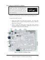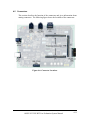
1
ADSP-21535 EZ-KIT LITE Evaluation System Manual Second Edition, May 2002 Part Number 82-000603-01 Analog Devices, Inc. Digital Signal Processing Division One Technology Way Norwood, MA 02062-9106 a Limited Warranty The EZ-KIT Lite evaluation system is warranted against defects in materials and workmanship for a period of one year from the date of purchase from Analog Devices or from an authorized dealer. Disclaimer Analog Devices, Inc. reserves the right to change this product without prior notice. Information furnished by Analog Devices is believed to be accurate and reliable. However, no responsibility is assumed by Analog Devices for its use; nor for any infringement of patents or other rights of third parties, which may result from its use. No license is granted by implication or otherwise under the patent rights of Analog Devices, Inc. Trademark and Service Mark Notice EZ-KIT Lite, VisualDSP++, VisualDSP++ logo, CROSSCORE, CROSSCORE logo, Blackfin and the Blackfin logo are trademarks of Analog Devices Inc. SoundMAX, EZ-ICE, SHARC, the SHARC logo, TigerSHARC, and the TigerSHARC logo, are registered trademarks of Analog Devices, Inc. All trademarks and logos are property of their respective holders. Microsoft and Windows are registered trademarks of Microsoft Corporation. Adobe and Acrobat are trademarks of Adobe Systems Incorporated. PSDsoft Express and FlashLINK are trademarks of ST Microelectronics All other brand and product names are trademarks or service marks of their respective owners. ADSP-21535 EZ-KIT Lite Evaluation System Manual ii Regulatory Compliance The ADSP-21535 EZ-KIT Lite evaluation system has been certified to comply with the essential requirements of the European EMC directive 89/336/EEC (inclusive 93/68/EEC) and therefore carries the “CE” mark. The ADSP-21535 EZ-KIT Lite evaluation system had been appended to the Technical Construction File referenced ‘DSPTOOLS1’ dated December 21, 1997 and was awarded CE Certification by an appointed European Competent Body as listed below. Technical Certificate No: Issued by: Z600ANA1.007 Technology International (Europe) Limited 41 Shrivenham Hundred Business Park Shrivenham, Swindon, SN6 8TZ, UK The EZ-KIT Lite evaluation system contains ESD (electrostatic discharge) sensitive devices. Electrostatic charges readily accumulate on the human body and equipment and can discharge without detection. Permanent damage may occur on devices subjected to high-energy discharges. Proper ESD precautions are recommended to avoid performance degradation or loss of functionality. Store unused EZ-KIT Lite boards in the protective shipping package. ADSP-21535 EZ-KIT Lite Evaluation System Manual iii TABLE OF CONTENTS LIST OF TABLES............................................................................................................. vi LIST OF FIGURES ........................................................................................................... vi 1 INTRODUCTION.................................................................................................. 1-1 1.1 For More Information About Analog Devices Products................................. 1-2 1.2 For Technical or Customer Support ................................................................ 1-3 1.3 Purpose of This Manual .................................................................................. 1-3 1.4 Intended Audience........................................................................................... 1-3 1.5 Manual Contents ............................................................................................. 1-4 1.6 Online Help ..................................................................................................... 1-4 2 GETTING STARTED............................................................................................ 2-1 2.1 Overview ......................................................................................................... 2-1 2.2 Contents of your EZ-KIT Lite Package .......................................................... 2-1 2.3 PC Configuration............................................................................................. 2-2 2.4 Installation Tasks............................................................................................. 2-2 2.4.1 Installing the VisualDSP++ Software ...................................................... 2-3 2.4.2 Installing the VisualDSP++ License ........................................................ 2-3 2.4.3 Installing the EZ-KIT Lite Debug Software............................................. 2-3 2.4.4 Setting Up the EZ-KIT Lite Hardware .................................................... 2-4 2.4.5 Installing the EZ-KIT Lite USB Driver.................................................... 2-5 2.4.6 Verifying Driver Installation .................................................................. 2-14 2.4.7 Starting VisualDSP++ ............................................................................ 2-15 3 USING THE EZ-KIT LITE ................................................................................... 3-1 3.1 Overview ......................................................................................................... 3-1 3.2 EZ-KIT Lite License Restrictions ................................................................... 3-2 3.3 Memory Map................................................................................................... 3-2 3.4 Using the SDRAM Interface ........................................................................... 3-3 3.5 Using Flash Memory....................................................................................... 3-3 3.6 Using the Programmable Flag Pins................................................................. 3-5 3.6.1 Using the Power Management Features ................................................... 3-6 3.7 Example Programs .......................................................................................... 3-6 3.8 Using the Flash Programmer Utility ............................................................... 3-6 4 EZ-KIT LITE HARDWARE REFERENCE ......................................................... 4-1 4.1 Overview ......................................................................................................... 4-1 4.2 System Architecture ........................................................................................ 4-2 4.2.1 External Bus Interface .............................................................................. 4-3 4.2.2 SPORT0 – Audio Interface....................................................................... 4-3 4.2.3 Expansion Interface .................................................................................. 4-4 4.2.4 JTAG Emulation Port ............................................................................... 4-4 4.3 Jumper and DIP Switch Settings..................................................................... 4-5 4.3.1 Audio Input Select Jumper (JP1).............................................................. 4-5 4.3.2 Audio Codec Disable Jumper (JP2).......................................................... 4-6 4.3.3 Boot Mode Select Switch (SW1).............................................................. 4-6 4.3.4 DSP PLL Setup Switch (SW2)................................................................. 4-6 4.4 LEDs and Push Buttons................................................................................... 4-8 ADSP-21535 EZ-KIT Lite Evaluation System Manual iv 4.4.1 Programmable Flag LEDs (LED1, LED2, LED3, LED4) ....................... 4-9 4.4.2 USB Monitor LED (LED5) ...................................................................... 4-9 4.4.3 Power LED (LED6).................................................................................. 4-9 4.4.4 Reset LEDs (LED7, LED8)...................................................................... 4-9 4.4.5 Non-Maskable Interrupt Push Button (SW3) ........................................... 4-9 4.4.6 Programmable Flag Push Buttons (SW4, SW5, SW6, SW7)................. 4-10 4.4.7 Reset Push Button (SW8) ....................................................................... 4-10 4.5 Connectors..................................................................................................... 4-11 4.5.1 Expansion Interface (P1, P2, P3)............................................................ 4-12 4.5.2 FlashLINK (P4) ...................................................................................... 4-12 4.5.3 Audio (P5, P6) ........................................................................................ 4-12 4.5.4 USB (P7)................................................................................................. 4-13 4.5.5 JTAG (P8)............................................................................................... 4-13 4.5.6 SPORT0 (P9).......................................................................................... 4-14 4.5.7 Power Connector (P10) .......................................................................... 4-14 4.6 Specifications ................................................................................................ 4-14 4.6.1 Power Supply.......................................................................................... 4-15 4.6.2 Board Current Measurements................................................................. 4-15 4.6.3 Mechanical Dimensions ........................................................................... 4-1 APPENDIX A: BILL OF MATERIALS........................................................................... A APPENDIX B: SCHEMATIC............................................................................................E INDEX ................................................................................................................................ 1 ADSP-21535 EZ-KIT Lite Evaluation System Manual v LIST OF TABLES Table 1-1: Related DSP Documents ................................................................................ 1-5 Table 1-2: Related VisualDSP++ Documents ................................................................. 1-5 Table 2-1: Minimum PC Configuration........................................................................... 2-2 Table 3-1: EZ-KIT Lite Evaluation Board Memory Map ............................................... 3-2 Table 3-2: SDRAM Default Settings............................................................................... 3-3 Table 3-3: Programmable Flag Pin Summary ................................................................. 3-5 Table 3-4: Power Management PF Settings..................................................................... 3-6 Table 4-1: Connector Interfaces....................................................................................... 4-4 Table 4-2: Boot Mode Select Switch (SW1) Settings ..................................................... 4-6 Table 4-3: PLL Setup Switch (SW2) Functions .............................................................. 4-7 Table 4-4: Programmable Flag LEDs .............................................................................. 4-9 Table 4-5: Programmable Flag Switches....................................................................... 4-10 Table 4-6: Power Connector .......................................................................................... 4-15 Table 4-7: Current Measurement Resistors ................................................................... 4-15 LIST OF FIGURES Figure 2-1: EZ-KIT Lite Hardware Setup ....................................................................... 2-4 Figure 2-2: Add New Hardware Wizard Dialog Box ...................................................... 2-5 Figure 2-3: Search for the driver...................................................................................... 2-6 Figure 2-4: Search the CD-ROM..................................................................................... 2-6 Figure 2-5: The driver is located...................................................................................... 2-7 Figure 2-6: Search for .sys File Dialog Box .................................................................... 2-7 Figure 2-7: Open the .sys File.......................................................................................... 2-8 Figure 2-8: Copying Files ................................................................................................ 2-8 Figure 2-9: Finish the Software Installation .................................................................... 2-9 Figure 2-10: Found New Hardware Wizard .................................................................. 2-10 Figure 2-11: Search for a Suitable Driver...................................................................... 2-11 Figure 2-12: Locate Driver Files.................................................................................... 2-12 Figure 2-13: Driver File Search Results ....................................................................... 2-13 Figure 2-14: Completing Driver Installation Dialog Box.............................................. 2-14 Figure 2-15: New Session Dialog Box .......................................................................... 2-15 Figure 3-1: Flash Memory Map....................................................................................... 3-4 Figure 4-1: System Architecture...................................................................................... 4-2 Figure 4-2: Jumper Locations .......................................................................................... 4-5 Figure 4-3: Audio Input Jumper Settings (JP1) ............................................................... 4-6 Figure 4-4: Default PLL Setup Switch Settings (SW2)................................................... 4-7 Figure 4-5: LED and Push Button Locations................................................................... 4-8 Figure 4-6: Connector Locations ................................................................................... 4-11 Figure 4-7: Mechanical Drawing ..................................................................................... 4-1 ADSP-21535 EZ-KIT Lite Evaluation System Manual vi 1 INTRODUCTION Thank you for purchasing the ADSP-21535 EZ-KIT Lite evaluation system. The evaluation board is designed to be used in conjunction with the VisualDSP++ development environment to test the capabilities of the ADSP21535 digital signal processor (DSP). The VisualDSP++ development environment gives you the ability to perform advanced application code development and debug such as: • • • • • Create, compile, assemble, and link application programs written in C++, C and ADSP-2153x assembly Load, run, step, halt, and set breakpoints in application programs Read and write data and program memory Read and write core and peripheral registers Plot memory Access to the ADSP-21535 from a PC is achieved through a USB port or an optional JTAG emulator. The USB interface gives unrestricted access to the ADSP-21535 DSP and the evaluation board peripherals. Analog Devices JTAG emulators offer faster communication between the host PC and target hardware. Analog Devices carries a wide range of in-circuit emulation products. To learn more about Analog Devices emulators and DSP development tools, go to http://www.analog.com/dsp/tools/. ADSP-21535 EZ-KIT Lite provides example programs to demonstrate the capabilities of the evaluation board. NOTE: The VisualDSP++ license provided with this EZ-KIT Lite evaluation system limits the use of internal memory to 176KB. The board’s features include: • • Analog Devices ADSP-21535 DSP o 300 MHz Core Clock Speed – default o Core Clock Speed – switch configurable o Boot Mode – switch configurable USB Debugging Interface o NOTE: this is not the DSP’s USB interface ADSP-21535 EZ-KIT Lite Evaluation System Manual 1-1 • • • • • • • Analog Devices AD1885 48 kHz AC’97 SoundMAX Codec o Jumper-Selectable Line-In or Mic-In 3.5 mm Stereo Jack o Line-Out 3.5 mm Stereo Jack SDRAM o 4 M x 32-bit Flash Memory o 272 K x 16 Interface Connectors o 14-Pin Emulator Connector for JTAG Interface o SPORT0 Connector o FlashLINKTM Connector (for flash programming) o Expansion Interface Connectors (not populated) General-Purpose I/O o 4 Push Buttons connected to DSP Programmable Flags o 1 Push Button connected to DSP Non-maskable Interrupt o 4 LEDs connected to DSP Programmable Flags Real Time Clock Analog Devices ADP3331, ADP3338, ADP3339 & ADP3088 Voltage Regulators The EZ-KIT Lite board has a flash memory device that can be used to store user specific boot code. By configuring the boot mode switch (SW1) and by programming the flash, the board can run as a stand-alone unit. For information about using the flash, see section 3.5. SPORT0 is interfaced with an audio Codec, allowing you to create audio signal processing applications. SPORT0 is also attached to an off-board connector to allow communication with other serial devices. For information about SPORT0, see section 4.2.2. Additionally, the EZ-KIT Lite board provides access to most of the DSP’s peripheral ports. Access is provided in the form of uninstalled expansion interface connectors. These DSP’s USB pins are brought to this connector, but require additional circuitry to function as a USB port. The PCI bus of the DSP is not available at any connector of the EZ-Kit Lite. For information about the expansion interface, see section 4.2.3. 1.1 For More Information About Analog Devices Products Analog Devices can be accessed on the Internet at http://www.analog.com. You can directly access the DSP Web pages at http://www.analog.com/dsp. This page provides access to DSP-specific technical information and documentation, product overviews, and product announcements. For specific information about DSP tools, go to http://www.analog.com/dsp/tools. ADSP-21535 EZ-KIT Lite Evaluation System Manual 1-2 You may also obtain additional information about Analog Devices and its products in any of the following ways: 1.2 • FAX questions or requests for information to (781) 461-3010. • Access the Computer Products Division File Transfer Protocol (FTP) site at 137.71.23.21 or ftp://ftp.analog.com. For Technical or Customer Support You can reach our Customer Support group in the following ways: • Contact your local Analog Devices sales office or an authorized Analog Devices distributor. • Call: (800)-ANALOGD 1.3 • E-mail general DSP questions to: [email protected] [email protected] (European customer support) • E-mail DSP Tools questions to: [email protected] • Submit a DSP Tools Technical Support Form: http://forms.analog.com/Form_Pages/DSP/tools/contactDSP.asp Purpose of This Manual The ADSP-21535 EZ-KIT Lite Evaluation System Manual provides instructions for using the hardware and installing the software on your PC. This manual provides guidelines for running your own code on the ADSP-21535 EZ-KIT Lite. This manual also provides a description of the use and configuration of the components on the evaluation board. Finally, a schematic and a bill of materials are provided as reference for future ADSP-21535 board designs. 1.4 Intended Audience This manual is a user’s guide and reference to the ADSP-21535 EZ-KIT Lite evaluation system. DSP programmers who are familiar with the Analog Devices Blackfin DSP architecture, operation, and programming are the primary audience for this manual. ADSP-21535 EZ-KIT Lite Evaluation System Manual 1-3 DSP programmers who are unfamiliar with Analog Devices Blackfin DSPs can use this manual in conjunction with the ADSP-21535 DSP Hardware Reference and the ADSP-21535 DSP Instruction Set, which describe the DSP architecture and instruction set. DSP programmers who are unfamiliar with VisualDSP++ should refer to the VisualDSP++ Help menu and the VisualDSP++ User’s Guide. For the locations of these documents, refer to section 1.6. 1.5 Manual Contents This manual contains the following information: 1.6 • Chapter 1 — Introduction Provides manual information and Analog Devices contact information. • Chapter 2 — Getting Started Provides software and hardware installation procedures, PC system requirements, and basic board information. • Chapter 3 — Using the EZ-KIT Lite Provides information on the EZ-KIT Lite from a programmers perspective, and provides an easy-to-access memory map. • Chapter 4 — EZ-KIT Lite Hardware Reference Provides information on the hardware aspects of the evaluation system. • Appendix A — Bill of Materials Provides a list of components used to manufacture the EZ-KIT Lite board. • Appendix B — Schematics Provides the resources to allow EZ-KIT Lite board-level debugging or to use as a reference design. Online Help Your software installation kit includes online Help as part of the Windows interface. These help files provide information about VisualDSP++ and the ADSP-21535 EZ-KIT Lite evaluation system. To view VisualDSP++ Help, click on the Help menu item or go to the Windows task bar and select Start\Programs\VisualDSP\VisualDSP++ Help. ADSP-21535 EZ-KIT Lite Evaluation System Manual 1-4 To view help on additional ADSP-21535 EZ-KIT Lite features, go to the windows task bar and select Start\Programs\VisualDSP\EZ-KIT Help. The documents in the following tables can be found through online Help or in the Docs folder of your VisualDSP++ installation. For more documentation, please go to http://www.analog.com/technology/dsp/library.html. Table 1-1: Related DSP Documents Document Name ADSP-21535 DSP Datasheet ADSP-21535 SHARC DSP Hardware Reference Blackfin DSP Instruction Set Reference Description General functional description, pinout, and timing. Description of internal DSP architecture and all register functions. Description of all allowed DSP assembly instructions. Table 1-2: Related VisualDSP++ Documents Document Name VisualDSP++ 2.0 Users Guide for BLACKfin DSPs VisualDSP++ 2.0 Assembler & Preprocessor Manual for BLACKfin DSPs VisualDSP++ 2.0 C/C++ Complier and Library Manual for BLACKfin DSPs VisualDSP++ 2.0 Linker & Utilities Manual for BLACKfin DSPs Description Detailed description of VisualDSP++ 2.0 features and usage. Description of the assembler function and commands for Blackfin family DSPs Description of the complier function and commands for Blackfin family DSPs Description of the linker function and commands for the Blackfin family DSPs ! Important: If you plan to use the EZ-KIT Lite board in conjunction with a JTAG emulator, refer to the documentation that accompanies the emulator. ADSP-21535 EZ-KIT Lite Evaluation System Manual 1-5 2 GETTING STARTED 2.1 Overview This chapter provides the information you need to begin using ADSP-21535 EZ-KIT Lite evaluation system. For correct operation install the software and hardware in the order presented in section 2.4. This chapter has the following sections: 2.2 • Contents of your EZ-KIT Lite Package (Section 2.2) Provides a list of the components that are shipped with this EZKIT Lite evaluation system. • PC Configuration (Section 2.3) Describes the minimum requirements for the PC to work with the EZ-KIT Lite evaluation system. • Installation Tasks (Section 2.4) Describes the step-by-step procedure for setting up the hardware and software. Contents of your EZ-KIT Lite Package Your ADSP-21535 EZ-KIT Lite evaluation system package contains the following items. • • • • • • • • EZ-KIT Lite Quick Start Guide ADSP-21535 EZ-KIT Lite board VisualDSP++ CD with license. ADSP-21535 EZ-KIT Lite CD, containing: o EZ-KIT Lite specific debug software o USB driver files o Example programs o ADSP-21535 EZ-KIT Lite manual (this document) o Flash Programmer Utility Installation Quick Reference Card for VisualDSP++ Universal 7.5V DC power supply 5 meter USB type A to type B cable Registration card - please fill out and return If any item is missing, contact the vendor where you purchased your EZ-KIT Lite or contact Analog Devices, Inc. ADSP-21535 EZ-KIT Lite Evaluation System Manual 2-1 The EZ-KIT Lite evaluation system contains ESD (electrostatic discharge) sensitive devices. Electrostatic charges readily accumulate on the human body and equipment and can discharge without detection. Permanent damage may occur on devices subjected to high-energy discharges. Proper ESD precautions are recommended to avoid performance degradation or loss of functionality. Store unused EZ-KIT Lite boards in the protective shipping package. 2.3 PC Configuration For correct operation of the VisualDSP++ software and the EZ-KIT Lite, your computer must have the minimum configuration shown in Table 2-1. Table 2-1: Minimum PC Configuration Windows 98, Windows 2000 Intel (or comparable) 166MHz processor VGA Monitor and color video card 2-button mouse 50 MB free on hard drive 32 MB RAM Full-speed USB port CD-ROM Drive ! NOTE: This EZ-KIT Lite does not run under Windows 95 or Windows NT. 2.4 Installation Tasks The following tasks are provided for the safe and effective use of the ADSP21535 EZ-KIT Lite. Follow these instructions in the order presented to ensure correct operation of your software and hardware. 1. 2. 3. 4. 5. 6. 7. VisualDSP++ software installation VisualDSP++ license installation EZ-KIT Lite debug software installation EZ-KIT Lite hardware setup EZ-KIT Lite USB driver installation USB driver installation verification VisualDSP++ startup ADSP-21535 EZ-KIT Lite Evaluation System Manual 2-2 2.4.1 Installing the VisualDSP++ Software This EZ-KIT Lite comes with the latest version of VisualDSP++ for the Blackfin DSP family. You must install this software before installing the EZ-KIT Lite debug software. Insert the VisualDSP++ CD-ROM into the CD-ROM drive. If Auto Run is enabled on your PC, the home screen of the VisualDSP++ install wizard will automatically appear. If not, choose Run from the Start menu, and enter D:\Setup.exe in the Open field, where D is the name of your local CD-ROM drive. Click on the Install VisualDSP++ option. This will launch the setup wizard. Follow the on-screen instructions. 2.4.2 Installing the VisualDSP++ License Before the VisualDSP++ software can be used, the license must be installed. To install the VisualDSP++ license: 1. Ensure that VisualDSP++ has been installed first. 2. Insert the VisualDSP++ CD-ROM into the CD-ROM drive if it is not already in the drive. 3. Once the CD-ROM browser appears, select the Install License option. 4. Follow the setup wizard instructions. ! NOTE: You will need the serial number located on the back of the CDROM sleeve. 2.4.3 Installing the EZ-KIT Lite Debug Software VisualDSP++ communicates with the EZ-KIT Lite board using the EZ-KIT Lite debug software. This software is supplied on the EZ-KIT Lite CD-ROM. To install the EZ-KIT Lite debug software: 1. Ensure that VisualDSP++ has been installed first. 2. Close all Windows applications. The install will not work correctly if any VisualDSP++ applications are running. 3. Insert the EZ-KIT Lite CD-ROM into the CD-ROM drive. If Autorun is enabled on your PC, the home screen of the EZ-KIT Lite install wizard will automatically appear. If not, choose Run from the Start menu, and enter D:\Setup.exe in the Open field, where D is the name of you local CD-ROM drive. Click the Install EZ-KIT Lite Software option. This will launch the setup wizard. Follow this wizard with the on-screen instructions. ADSP-21535 EZ-KIT Lite Evaluation System Manual 2-3 2.4.4 Setting Up the EZ-KIT Lite Hardware The EZ-KIT Lite evaluation system contains ESD (electrostatic discharge) sensitive devices. Electrostatic charges readily accumulate on the human body and equipment and can discharge without detection. Permanent damage may occur on devices subjected to high-energy discharges. Proper ESD precautions are recommended to avoid performance degradation or loss of functionality. Store unused EZ-KIT Lite boards in the protective shipping package. The ADSP-21535 EZ-KIT Lite board is designed to run outside your personal computer as a stand-alone unit. You do not have to open your computer case. To connect the EZ-KIT Lite board: 1. Remove the EZ-KIT Lite board from the package. Be careful when handling the board to avoid the discharge of static electricity, which may damage some components. 2. Figure 2-1 shows the default jumper settings, DIP Switch, connector locations, and LEDs used in installation. Confirm that your board is set up in the default configuration before continuing. Figure 2-1: EZ-KIT Lite Hardware Setup ADSP-21535 EZ-KIT Lite Evaluation System Manual 2-4 3. Plug the provided power supply into P10 on the EZ-KIT Lite board. Visually verify that the green power LED (LED6) is on. Also verify that the two red reset LEDs (LED7 and LED8) go on for a moment and then go off. 4. Connect the USB cable to an available full speed USB Port and to P7 on the ADSP-21535 EZ-KIT Lite board. 2.4.5 Installing the EZ-KIT Lite USB Driver The EZ-KIT Lite evaluation system can be installed on Windows 98 and Windows 2000 and requires one full-speed USB port. Section 2.4.5.1 describes the installation on Windows 98. Section 2.4.5.2 describes the installation on Windows 2000. 2.4.5.1 Windows 98 USB Driver Installation Before using the ADSP-21535 EZ-KIT Lite for the first time, the Windows 98 USB driver must first be installed. To install the USB driver: 1. Insert the EZ-KIT Lite CD-ROM into the CD-ROM drive. The connection of the device to the USB port will activate the Windows 98 “Add New Hardware Wizard” as shown in Figure 2-2. Figure 2-2: Add New Hardware Wizard Dialog Box ADSP-21535 EZ-KIT Lite Evaluation System Manual 2-5 2. Click Next. 3. Select Search for the best driver for your device as shown in Figure 2-3. Figure 2-3: Search for the driver 4. Click Next. 5. Select CD-ROM drive as shown in Figure 2-4. Figure 2-4: Search the CD-ROM 6. Click Next. ADSP-21535 EZ-KIT Lite Evaluation System Manual 2-6 Windows 98 will locate the WmUSBEz.inf file that is on the CD-ROM as shown in Figure 2-5. Figure 2-5: The driver is located 7. Click Next. The Coping Files dialog box appears (Figure 2-6). Figure 2-6: Search for .sys File Dialog Box 8. Click Browse. ADSP-21535 EZ-KIT Lite Evaluation System Manual 2-7 Figure 2-7 will appear. Figure 2-7: Open the .sys File 9. In Drives select your CD-ROM drive. 10. Click OK. Figure 2-8 will appear. Figure 2-8: Copying Files 11. Click OK. ADSP-21535 EZ-KIT Lite Evaluation System Manual 2-8 The driver installation is now complete as shown in Figure 2-9. Figure 2-9: Finish the Software Installation 12. Click Finish to exit the wizard. Verify the installation by following the instructions in section 2.4.6. ADSP-21535 EZ-KIT Lite Evaluation System Manual 2-9 2.4.5.2 Windows 2000 USB Driver Installation Before using the ADSP-21535 EZ-KIT Lite for the first time, the Windows 2000 USB driver must first be installed. To install the USB Driver: 1. Insert the EZ-KIT Lite CD-ROM into the CD-ROM drive. The connection of the device to the USB port will activate the Windows 2000 “Found New Hardware Wizard” as shown in Figure 2-10. Figure 2-10: Found New Hardware Wizard 2. Click Next. ADSP-21535 EZ-KIT Lite Evaluation System Manual 2-10 3. Select Search for a suitable driver for my device as shown in Figure 2-11. Figure 2-11: Search for a Suitable Driver 4. Click Next. ADSP-21535 EZ-KIT Lite Evaluation System Manual 2-11 5. Ensure that CD-ROM drives is selected as shown in Figure 2-12. Figure 2-12: Locate Driver Files 6. Click Next. ADSP-21535 EZ-KIT Lite Evaluation System Manual 2-12 Figure 2-13 appears. Figure 2-13: Driver File Search Results 7. Click Next. ADSP-21535 EZ-KIT Lite Evaluation System Manual 2-13 Windows 2000 will automatically install the ADSP-21535 EZ-KIT Lite driver. The driver installation is now complete as shown in Figure 2-14. Figure 2-14: Completing Driver Installation Dialog Box 8. Click Finish to exit the wizard. Verify the installation by following the instructions in section 2.4.6. 2.4.6 Verifying Driver Installation Before you use the EZ-KIT Lite evaluation system, verify that the USB driver software is installed properly: 1. Ensure that the USB cable is connected to the evaluation board and the PC. 2. Verify that the yellow USB monitor LED (LED5) is lit. This signifies that the board is communicating properly with the host PC and is ready to run VisualDSP++. ADSP-21535 EZ-KIT Lite Evaluation System Manual 2-14 2.4.7 Starting VisualDSP++ To start debugging, set up a session in VisualDSP++. 1. Verify that the yellow USB monitor LED (LED5, located near the USB connector) is lit. This signifies that the board is communicating properly with the host PC, and is ready to run VisualDSP++. 2. Hold down the Control (CTRL) key. 3. Select the Start button on the Windows taskbar, and then choose Programs\VisualDSP\VisualDSP++. The Session List dialog box appears if you already have existing sessions. Skip to step 4 if this is the first time running VisualDSP++. 4. Click on New Session. 5. The New Selection dialog will appear as shown in Figure 2-15. Figure 2-15: New Session Dialog Box 6. In Debug Target, choose EZ-KIT Lite (ADSP-21535). 7. Type a new target name in Session Name or accept the default name. 8. Click OK to return to the Session List. Highlight the new session and click Activate. ADSP-21535 EZ-KIT Lite Evaluation System Manual 2-15 3 USING THE EZ-KIT LITE 3.1 Overview This chapter provides specific information to assist you with developing programs for the ADSP-21535 EZ-KIT Lite board. This information appears in the following sections: • EZ-KIT Lite License Restrictions (Section 3.2) Describes the restrictions of the VisualDSP++ license shipped with the EZ-KIT Lite. • Memory Map (Section 3.3) Defines the memory map to assist in developing programs for the EZ-KIT Lite evaluation system. • Using the SDRAM Interface (Section 3.4) Defines the register values to configure the on-board SDRAM. • Using Flash Memory (Section 3.5) Describes how to program and use the on-board flash memory. • Using the Programmable Flag Pins (Section 3.6) Describes the function and use of the programmable flag pins on the EZ-KIT Lite evaluation system. • Example Programs (Section 3.7) Provides information about the example programs included in the ADSP-21535 EZ-KIT Lite evaluation system. • Using the Flash Programmer Utility (Section 3.8) Provides information on the Flash Programmer Utility included with the EZ-KIT Lite software. For more detailed information about programming the ADSP-21535, see the documents referred to in section 1.6. ADSP-21535 EZ-KIT Lite Evaluation System Manual 3-1 3.2 EZ-KIT Lite License Restrictions The license shipped with the EZ-KIT Lite imposes the following restrictions: • • • 3.3 Internal Memory space is limited to 176 KB of the ADSP-21535 internal memory space No connections to Simulator or Emulator sessions are allowed. Only one EZ-KIT Lite can be connected to the host PC and debugged at a time Memory Map The ADSP-21535 has internal SRAM that can be used for instruction storage or data storage. The configuration of internal SRAM is detailed in the ADSP-21535 DSP Hardware Reference. The ADSP-21535 EZ-KIT Lite board contains 272K x 16 bits of external flash memory. This memory is connected to the DSP’s ~AMS0 memory select pin. The external memory interface is also connected to 4M x 32-bit SDRAM memory. This memory is connected to the ~SMS0 pin. Table 3-1: EZ-KIT Lite Evaluation Board Memory Map External Memory Internal Memory Start Address 0x0000 0000 End Address 0x00FF FFFF 0x2000 0000 0x2009 FFFF All other locations 0xF000 0000 0xF003 FFFF 0xFF80 0000 0xFF80 3FFF 0xFF90 0000 0xFF90 3FFF 0xFFA0 0000 0xFFA0 3FFF 0xFFB0 0000 0xFFB0 0FFF 0xFFC0 0000 0xFFDF FFFF 0xFFE0 0000 0xFFFF FFFF All other locations Content SDRAM Bank 0 (SDRAM) See section 3.4 ASYNC Memory Bank 0 (FLASH) See section 3.5 Not used L2 SRAM 256 KB Data Bank A 16 KB Data Bank B 16 KB Instruction SRAM 16 KB Scratch Pad SRAM 4 KB System MMRs 2 MB Core MMRs 2 MB Reserved ADSP-21535 EZ-KIT Lite Evaluation System Manual 3-2 3.4 Using the SDRAM Interface In order to use the 4M x 32 bits (16 MB) of SDRAM memory, the three SDRAM control registers must be initialized. The following table shows the standard configuration for these registers when using the EZ-KIT Lite in the default configuration. These numbers were derived using the M48LC4M16ATG-75 with a system clock frequency of 120 MHz. Table 3-2: SDRAM Default Settings Register Value EBIU_SDRRC 0x0000074A EBIU_SDBCTL 0x00000001 EBIU_SDGCTL 0x0091998F Function RDIV = 1866 clock cycles Bank 0 enabled Bank 0 size = 16 MB Bank 0 column address width = 8 bits 32 bit data path External buffering timing disabled tWR = 2 SCLK cycles tRCD = 3 SCLK cycles tRP = 3 SCLK cycles tRAS = 6 SCLK cycles pre-fetch disabled CAS latency = 3 SCLK cycles SCLK1 disabled If you are in an EZ-KIT Lite session (that is, not using an emulator), the SDRAM registers are configured automatically through the debugger. The debugger uses the values in Table 3-2 whenever bank 0 is accessed through the debugger (such as viewing memory windows or loading a program). Clearing the appropriate checkbox on the Target Options dialog box, which is accessible through the Settings pull-down menu, disables this feature and allows manual configuration. An example program is included in the EZ-KIT installation directory, which demonstrates how to setup the SDRAM interface. 3.5 Using Flash Memory The DSM2150 Flash/PLD chip provides a total of 272K x 16 bits of external flash memory, arranged into two independent flash arrays (boot and main). The chip also has a series of configuration registers to control I/O and PLD. This chip is initially configured with the memory sectors mapped to the DSP as shown below in Figure 3-1. ADSP-21535 EZ-KIT Lite Evaluation System Manual 3-3 0x200A 0000 Main Flash Array 0x2002 0000 Empty 0x2001 00FF Config 0x2001 0000 Empty 0x2000 8000 0x2000 0000 Boot Flash Array Figure 3-1: Flash Memory Map Use PSDsoft ExpressTM to modify the default settings for the flash memory, the DSM project must be modified and the flash must be reprogrammed using FlashLINKTM. The default project files can be found in, \…\VisualDSP\Blackfin\EZ-KITs\ADSP-21535\DSMConfigFiles. Analog Devices does not provide any support for setting up the DSM2150 with PSDsoft ExpressTM or programming it using FlashLINKTM. Email STMicroelectronics for technical assistance at [email protected]. To program the flash with your boot code, you must first create a loader file from your DSP code. You will need to set up the loader in VisualDSP++ depending on how you will be booting the flash. The two possibilities are to boot the DSP in 16-bit external execution mode or in 8-bit boot mode. See section 4.3.3 for the boot mode settings. Next, the loader file must be programmed into the flash. This can be done through the DSP using the VisualDSP++ Flash Programmer Utility (see section 3.8) or using by using the FlashLink programmer. The DSM2150 can be reprogrammed using the FlashLINKTM JTAG programming cable available from STMicoreclectronics (www.st.com/psd) for approximately $59. FlashLINKTM plugs into any PC parallel port. The software development tool, PSDsoft Express, is required to modify the configuration of the DSM2150 and operate the FlashLINKTM cable. PSDsoft ExpressTM can be downloaded at no charge from at www.st.com/psd. ADSP-21535 EZ-KIT Lite Evaluation System Manual 3-4 3.6 Using the Programmable Flag Pins The ADSP-21535 has 16 asynchronous Programmable Flag (PF) I/O pins. During reset PF0-PF9 function as inputs to the internal PLL of the DSP. They are not valid until 120uS after reset. Table 3-3 describes how the PFs are used on the EZ-KIT Lite. After a DSP reset, all of the PF pins are initialized as inputs. The direction of the PF is configured by the FIO_DIR Memory Mapped Register (MMR). The PFs are set high (1) using the FIO_FLAG_S and cleared (0) using the FIO_FLAG_C MMRs. For more information on configuring the PF pins, see the ADSP-21535 DSP Hardware Reference Manual. All of the PFs can are brought out to the expansion connector P2. The location of the PF nets can be found in APPENDIX B: SCHEMATIC. Table 3-3: Programmable Flag Pin Summary Flag PF0 PF1 PF2 PF3 PF4 PF5 PF6 PF7 PF8 PF9 PF10 PF11 PF12 PF13 PF14 PF15 Connected to LED4 LED1 LED2 LED3 SW4 SW5 SW6 SW7 PMGMT0 PMGMT1 PMGMT2 U7.11 Use PF0-3 are connected to the LEDs. These can be used to light an LED when a routine completes. PF4-7 are connected to the push buttons on the EZKIT Lite board and are for user input. Your routine can monitor and execute specific code when a push button has been pressed. Not used Not used Not used Not used These are used to change the internal voltage of the DSP. Refer to section 3.6.1 for more information. Connected to the reset of the AD1885 Codec (U7). This signal must be output as a high (1) to enable the AD1885 Codec. ADSP-21535 EZ-KIT Lite Evaluation System Manual 3-5 3.6.1 Using the Power Management Features PF14-PF12 allow you to program the core voltage of the DSP. The default core voltage is 1.5V. Table 3-4 gives the value of the core voltage corresponding to the state of these PFs. When lowering the core voltage of the DSP, the frequency of the DSP must be taken into consideration. As you lower the core voltage of the DSP, the frequency the core is running at must be decrease. Table 3-4: Power Management PF Settings PF14 PF13 0 0 0 0 0 1 0 1 1 0 1 0 * 1 1 1 1 * Denotes Default 3.7 PF12 0 1 0 1 0 1 0 1 VDD_INT 0.9V 1.0V 1.1V 1.2V 1.3V 1.4V 1.5V 1.6V Example Programs Example programs are provided with the ADSP-21535 EZ-KIT Lite demonstrate various capabilities of the evaluation board. These programs installed with the EZ-KIT Lite software and can be found \…\VisualDSP\Blackfin\EZ-KITs\ADSP-21535\Examples. Please refer to readme files provided with each example program for more information. 3.8 to are in the Using the Flash Programmer Utility The ADSP-21535 EZ-KIT Lite evaluation system includes a Flash Programmer Utility. The utility allows you to program the flash on the EZ-KIT Lite. This utility must be installed separately from the debug software. To install the utility, insert the EZ-KIT Lite CD-ROM and follow the steps in the installation wizard. After it has been installed, it is available from the Tools pull-down menu in VisualDSP++. For more information on the Flash Programmer Utility go to the Start menu and choose Programs\VisualDSP\Flash Programmer Help. ADSP-21535 EZ-KIT Lite Evaluation System Manual 3-6 4 EZ-KIT LITE HARDWARE REFERENCE 4.1 Overview This chapter describes the hardware design of the ADSP-21535 EZ-KIT Lite board. The following topics are covered: • System Architecture (Section 4.2) Describes the configuration of the DSP as well as a description of how all of the components on the board interface with the DSP. • Jumper and DIP Switch Settings (Section 4.3) Shows the location and describes the function of all the configuration jumpers and DIP Switches. • LEDs and Push Buttons (Section 4.4) Shows the location and describes the function of all the LEDs and push buttons. • Connectors (Section 4.5) Shows the location and gives the part number for all of the connectors on the board. Also, the manufacturer and part number information is given for the mating part. • Specifications (Section 4.6) Gives the requirements for powering the board. ADSP-21535 EZ-KIT Lite Evaluation System Manual 4-1 System Architecture The EZ-KIT Lite has been designed to demonstrate the capabilities of the ADSP21535 DSP. This section describes the DSP’s configuration on the EZ-KIT Lite board. JTAG Header 544KB Flash (U4) 4M X 32bit SDRAM (U5, U6) JTAG Port EZ USB FX USB Connector SRAM 20MHz Oscillator External Bus Interface Unit Power Management UART1:0 Timer2:0 ADSP-21535 SPORT1 DSP RTC (U1) USB Expansion Connectors (P1, P2, P3) VDD_INT 3.3V VDD_EXT SPORT0 LEDs, PBs and Clock Logic PF15:0 SPORT0 Connector 5V A5V 3.3V Power Regulation SPI 1:0 CLK_IN 32.768KHz Crystal +7.5V Connector 4.2 AD1885 Codec (U7) Stereo LINEIN/ MIC and LINEOUT Connectors Figure 4-1: System Architecture The DSP has a default core voltage of 1.5V. Refer to section 3.6.1 for more information about changing the core voltage while the DSP is running. The voltage of the DSP’s peripheral interface is 3.3V. A 20 MHz oscillator supplies the input clock to the DSP. The speed at which the core and peripherals operate is determined by the configuration of the multiplier select switch (SW2) at reset. (See section 4.3.4.) By default, the DSP core runs at 300 MHz and the peripheral interface runs at 120 MHz. A 32.768 kHz crystal supplies the Real Time Clock (RTC) inputs of the DSP The EZ-KIT Lite board can be configured to boot in all of the possible ADSP21535 boot modes. For information about configuring the boot mode, see section 4.3.3. ADSP-21535 EZ-KIT Lite Evaluation System Manual 4-2 4.2.1 External Bus Interface The External Bus Interface Unit (EBIU) is connected to 4M x 32 bits of SDRAM (16 MB). This memory is connected to the synchronous memory select 0 (~SMS0) pin. Refer to section 3.4 for information about configuring the SDRAM. The EBIU is also connected to 272K x 16 bits of flash memory. This memory is connected to the asynchronous memory select (~AMS0) pin. The DSP can use this memory both for booting and storing information during normal operation. Refer to section 3.5 for information about using the flash memory. All of the address, data, and control signals are available externally via the extender connectors (P1-3). The pinout of these connectors can be found in APPENDIX B: SCHEMATIC. 4.2.2 SPORT0 – Audio Interface SPORT0). is connected to the AD1885 SoundMAX Codec (U7). Two 3.5mm stereo jacks (P5, P6) allow audio to be input and output. You can supply an audio input to the Codec microphone input channel (MIC1) or to the stereo LINE_IN input channel. The jumper settings of JP1 determine the Codec channel driven by the input jack (P5). For information about configuring JP1, see section 4.3.1. SPORT0 is also routed to an off-board connector (P9). When using the off-board connector, the Codec must be held in reset, so that it does not drive any of the SPORT0 signals. The Codec can be held in reset by driving PF15 low or by setting up JP2 to always hold the Codec in reset (see section 4.3.2). PF15 must be pulled HI (1) for the Codec to function. ! NOTE: TCLK0 and RCLK0 pins are shorted together using R114 and R118. ADSP-21535 EZ-KIT Lite Evaluation System Manual 4-3 4.2.3 Expansion Interface The expansion interface consists of the footprints for 3 connectors. The following table shows the interfaces each connector provides. For the exact pin-out of these connectors refer to APPENDIX B: SCHEMATIC. Analog Devices does not populate these connectors or provide any additional support for this interface. The mechanical locations of these connectors can be found in section 4.6.3. Table 4-1: Connector Interfaces Connector Interfaces P1 5V, GND, Address, Data P2 3.3V, GND, EBUI control signals, PF0-15, SPI0-1, SPORT1, UART0-1, TMR0-2, NMI P3 1.5V, GND, Reset, USB, CLKOUT, SLEEP Limits to the current and to the interface speed must be taken into consideration if you use this interface. The maximum current limit is dependent on the regulator used and its capabilities. Additional circuitry can also add extra loading to signals, decreasing their maximum effective speed. ! Analog Devices does not support and is not responsible for the effects of additional circuitry. 4.2.4 JTAG Emulation Port The JTAG emulation port allows an emulator to access the DSP’s internal and external memory through a 6-pin interface. The JTAG emulation port of the DSP is also connected to the USB debugging interface (NOTE: This is not the DSP’s USB interface). When an emulator is connected to the board at P8, the USB debugging interface is disabled. See section 4.5.5 for more information about the JTAG connector. To learn more about available emulators, contact Analog Devices (see section 1.1). ADSP-21535 EZ-KIT Lite Evaluation System Manual 4-4 4.3 Jumper and DIP Switch Settings This section describes the function of all the jumpers and DIP switches. The following figure shows the location of all the jumpers and DIP switches. Figure 4-2: Jumper Locations 4.3.1 Audio Input Select Jumper (JP1) The audio input jack (P5) can be connected to the MIC1 or the LINEIN input channels of the AD1885 Codec (U7). When the JP1 jumpers connect pins 1 and 3 and pins 2 and 4, P3 connects to the mono MIC1 channel. When the jumpers connect pins 3 and 5 and pins 4 and 6, P5 connects to the stereo LINE_IN channel of the AD1885 Codec. These jumper settings are illustrated below in Figure 4-3. (The words MIC and LINE are on the board as a reference) ADSP-21535 EZ-KIT Lite Evaluation System Manual 4-5 MIC LINE MIC JP1 6 5 2 1 JP1 2 1 LINE Mono MIC1 Stereo LINE_IN (DEFAULT) 6 5 Figure 4-3: Audio Input Jumper Settings (JP1) 4.3.2 Audio Codec Disable Jumper (JP2) Placing a jumper between pins 1 and 2 of JP2 holds the AD1885 in reset, preventing it from driving signals to the serial port. When a jumper is between pins 2 and 3 of JP2, the AD1885 is held in reset until PF15 is set to an output and is asserted. These position are labeled on the board as “DIS” and “ENA 1885”. 4.3.3 Boot Mode Select Switch (SW1) The boot mode select switch determines how the DSP will boot. Table 4-2 shows the switch settings for the boot modes. NOTE: SPI ROM is not available on the EZ-KIT Lite. Table 4-2: Boot Mode Select Switch (SW1) Settings BMODE0 Pin 1 BMODE1 Pin 2 BMODE2 Pin 3 On On On Off On On On Off On Off Off On - - Off Function Execute from 16 bit external memory (no boot) Boot from 8-bit EPROM (Default) Boot from SPI0 ROM (8-bit addresses) Boot from SPI0 ROM (16-bit addresses) All others reserved 4.3.4 DSP PLL Setup Switch (SW2) The DSP’s Phase Lock Loop (PLL) multiplies the 20 MHz input clock by a multiplication factor to set the core clock speed of the DSP. Internal to the DSP the Programmable Flags, PF0-PF9, are multiplexed with the PLL setup signals, SSEL0-6, DF, and MSEL0-1. ADSP-21535 EZ-KIT Lite Evaluation System Manual 4-6 During reset, the function of these pins is to setup the PLL. At this time, these signals are attached to the PLL setup switch (SW2) and determine the core and external clock speeds of the DSP. Approximately 120uS after reset has been deasserted these pins are no longer attached to SW2, but function as PFs. The following table shows the switch position that corresponds to a DSP pin. Table 4-3: PLL Setup Switch (SW2) Functions DSP Pin Switch Position 1 2 3 4 5 6 7 8 9 10 11 12 MSEL0 MSEL1 MSEL2 MSEL3 MSEL4 MSEL5 MSEL6 DF SSEL0 SSEL1 None Bypass Figure 4-4 shows the default setting for SW2. This will produce a 300MHz core clock speed and a 120 MHz peripheral interface speed. For more information about setting up the multiplication factors, refer to the Managing DSP Clocks section of the ADSP-21535 DSP Hardware Reference. ON 1 2 3 4 5 6 7 8 9 10 11 12 Figure 4-4: Default PLL Setup Switch Settings (SW2) ! NOTE: A switch setting of “ON” supplies a logic low (0) on the corresponding DSP pin. ADSP-21535 EZ-KIT Lite Evaluation System Manual 4-7 4.4 LEDs and Push Buttons This section describes the function of all the LEDs and push buttons. Figure 4-5 shows the location of all the LEDs and push buttons. Figure 4-5: LED and Push Button Locations ADSP-21535 EZ-KIT Lite Evaluation System Manual 4-8 4.4.1 Programmable Flag LEDs (LED1, LED2, LED3, LED4) Four LEDs are connected to four of the DSP’s Programmable Flag (PF) pins, PF0-3. These LEDs are active HIGH and are lit by an output of “1” from the DSP. Refer to section 3.6 for more information about using of the PFs when programming the DSP. Table 4-4: Programmable Flag LEDs LED Reference Designator LED4 LED1 LED2 LED3 DSP Programmable Flag Pin PF0 PF1 PF2 PF3 4.4.2 USB Monitor LED (LED5) The USB Monitor LED (LED5) indicates that USB communication has been initialized successfully and you may connect to the DSP using a VisualDSP++ EZ-KIT Lite session. This should take approximately 15 seconds. If the LED does not light, try cycling power on the board and/or reinstalling the USB driver (see section 2.4.5). 4.4.3 Power LED (LED6) LED6 is a green LED that indicates when power is being properly supplied to the board. 4.4.4 Reset LEDs (LED7, LED8) When LED8 is lit, it indicates that the master reset of all the major ICs is active. When LED7 is lit, the USB interface chip (U11) is being reset. The USB chips will only reset on power-up, or if USB communication has not been initialized. 4.4.5 Non-Maskable Interrupt Push Button (SW3) SW3 is connected to the Non-maskable Interrupt (NMI) pin of the DSP. When pressed, the DSP will vector to the NMI interrupt vector. ADSP-21535 EZ-KIT Lite Evaluation System Manual 4-9 4.4.6 Programmable Flag Push Buttons (SW4, SW5, SW6, SW7) Four push buttons are provided for general-purpose user input. SW4-7 connect to the DSP’s Programmable Flag (PF) pins, PF4-7. The push buttons are active high and when pressed send a high (1) to the DSP. Refer to section 3.6 for more information about the use of the PFs when programming the DSP. Table 4-5 shows the PF signal and the switch it is connected to. Table 4-5: Programmable Flag Switches Push Button Reference Designator SW4 SW5 SW6 SW7 DSP Programmable Flag Pin PF4 PF5 PF6 PF7 4.4.7 Reset Push Button (SW8) The RESET push button resets all of the ICs on the board. This reset does not affect the USB interface chip (U11) unless communication has not been initialized with a PC. After USB communication has been initialized, the only way to reset the USB is by powering down the board. ADSP-21535 EZ-KIT Lite Evaluation System Manual 4-10 4.5 Connectors This section describes the function of the connectors and gives information about mating connectors. The following figure shows the locations of the connectors. Figure 4-6: Connector Locations ADSP-21535 EZ-KIT Lite Evaluation System Manual 4-11 4.5.1 Expansion Interface (P1, P2, P3) Three board-to-board connector footprints provide the signals for most of the DSP peripheral interfaces. Analog Devices does not populate these connectors or provide any additional support for this interface. See section 4.2.3, for more information on the Expansion Interface. Contact Samtec for the availability and pricing of these connectors. Part Description 90 Position 0.05” Spacing (P1, P2, P3) Manufacturer Samtec Mating Connector Samtec 90 Position 0.05” Spacing (Through Hole) 90 Position 0.05” Spacing (Surface Mount) 90 Position 0.05” Spacing (Low Cost) Part Number SFM-145-01-S-D TFM-145-x1 Series Samtec TFM-145-x2 Series Samtec TFC-145 Series 4.5.2 FlashLINK (P4) The FlashLINK connector allows you to configure and program the STMicroelectronics DSM2150 flash/PLD chip. See section 3.5, for more information about using the FlashLINK connector. Part Description Right-angle 7X2 Shrouded 0.1 spacing FlashLINK JTAG Programmer TM Manufacturer TYCO Mating Assembly ST Micro Part Number 2-767004-2 FL-101B 4.5.3 Audio (P5, P6) There are two 3.5mm stereo audio jacks: one input, and one output. Part Description 3.5mm stereo jack (P5, P6) 3.5mm stereo plug to 3.5mm stereo cable Manufacturer Shogyo Mating Cable Radio Shack Part Number SJ-0359AM-5 42-2387A ADSP-21535 EZ-KIT Lite Evaluation System Manual 4-12 4.5.4 USB (P7) The USB connector is a standard Type B USB receptacle. This connector is used to debug the DSP, and is not connected to the DSP’s USB interface. Part Description Type B USB receptacle (P7) Manufacturer Mill-Max Digi-Key Mating Connector USB cable (provided with kit) Assmann Digi-Key Part Number 897-30-004-90-000 ED90003-ND AK672-5 AK672-5ND 4.5.5 JTAG (P8) The JTAG header is the connecting point for a JTAG in-circuit emulator pod. When an emulator is connected to the JTAG header, the USB debug interface is disabled. ! NOTE: Pin 3 is missing to provide keying. Pin 3 in the mating connector should have a plug. ! NOTE: When using an emulator with the EZ-KIT Lite board, follow the connection instructions provided with the emulator. ADSP-21535 EZ-KIT Lite Evaluation System Manual 4-13 4.5.6 SPORT0 (P9) SPORT0 is connected to a 20-pin connector. The pinout for this connector can be found in APPENDIX B: SCHEMATIC. Contact AMP for pricing and availability on these connectors. Part Description Manufacturer 20 position AMPMODU system AMP 50 receptacle (P9) Mating Connectors 20 position AMPMODU system AMP 20 connector 20 position AMPMODU system AMP 20 connector (w/o lock) Flexible film contacts (20 per AMP connector) Mating Assembly Straight-through assembly with Gopher locking connector on each end Electronics Part Number 104069-1 2-487937-0 2-487938-0 487547-1 DRFFC10X7RHURHU5 4.5.7 Power Connector (P10) The power connector provides all of the power necessary to operate the EZ-KIT Lite board. Part Description 2.5mm Power Jack (P10) Manufacturer Part Number Switchcraft RAPC712 Digi-key SC1152-ND Mating Power Supply (shipped with EZ-KIT Lite) 7.5V Power Supply GlobTek TR9CC2000LCP-Y 4.6 Specifications This section provides the requirements for powering the board and the mechanical dimensions of the board. ADSP-21535 EZ-KIT Lite Evaluation System Manual 4-14 4.6.1 Power Supply The power connector supplies DC power to the EZ-KIT Lite board. Table 4-6 shows the power connector pinout. Table 4-6: Power Connector Terminal Center pin Outer Ring Connection +7.5 VDC@2amps GND 4.6.2 Board Current Measurements The ADSP-21535 EZ-KIT Lite board provides eight zero-ohm resistors that may be removed to measure current draw. Table 4-7 shows the resistor number, the voltage plane, and a description of the components on the plane. Table 4-7: Current Measurement Resistors Resistor Voltage Plane Description R2 VDD_RTC DSP Real Time Clock Supply R3 VDD_EXT DSP External Interface Supply R6 VDD_INT DSP Internal Interface Supply R7 VDD_PCIEXT R8 VDD_PLL R110 5V 5V Supply R111 3V 3V supply to all non DSP-related components R113 3V_DSP DSP PCI Interface Supply DSP Phase Lock Loop Supply 3V to DSP-related components ADSP-21535 EZ-KIT Lite Evaluation System Manual 4-15 4.6.3 Mechanical Dimensions The following figure shows the location of the mounting holes as well as the PIN1 of each of the expansion connectors. 5.000 4.750 3.875 P1 3.750 2.500 P2 1.400 1.300 1.125 P3 6.750 7.000 6.375 6.200 3.600 3.250 0.625 0.000 0.250 0.250 0.000 Figure 4-7: Mechanical Drawing ADSP-21535 EZ-KIT Lite Evaluation System Manual 4-1 APPENDIX A: BILL OF MATERIALS REF QTY. 2 3 3 1 4 1 5 1 6 1 7 1 8 1 9 1 10 3 11 1 12 1 13 1 14 1 15 1 16 2 17 1 18 1 19 1 20 2 21 2 22 1 23 1 Description 74LVC14A SOIC14 HEX-INVER-SCHMITT-TRIGGER IDT74FCT3244APY SSOP20 3.3V-OCTAL-BUFFER 24.576MHZ SMT OSC005 CRYSTAL CY7C64603-128 PQFP128 USB-TX/RX MICROCONTROLLER MMBT4401 SOT-23 NPN TRANSISTOR 200MA 74LVC00AD SOIC14 24LC00-SN SOIC8 128 BIT SERIAL EEPROM ADP3331ART SOT23-6 ADJ 200MA REGULATOR BSS123 SOT23D NMOS FET CY7C1019BV33-15VC SOJ32 128K X 8 SRAM SN74AHC1G02 SOT23-5 SINGLE-2 INPUT-NOR SN74LV164A SOIC14 8-BIT-PARALLEL-SERIAL CY7C4201V-15AC TQFP32 64-BYTE-FIFO 12.0MHZ THR OSC006 CRYSTAL MT48LC4M16 TSOP54 4MX16-SDRAM-133MHZ 32.768kHz TH OSC007 CRYSTAL SN74AHC1G00 SOT23-5 SINGLE-2-INPUT-NAND 21535 BRD DSM2150F5V U4"" BLKFIN160.OBJ SUM 876F5F1 1000pF 50V 5% 1206 CERM 0.1uF 50V 10% 1206 CERM ADM708SAR SOIC8 VOLTAGE-SUPERVISOR AD1885JST LQFP48 AC97 STEREO CODEC Ref. Des Manufacturer Part Number U9-10, U19 TI 74LVC14AD U24 IDT IDT74FCT3244APY Y2 EPSON MA505 24.576M-C2 U11 CYPRESS CY7C64603-128NC Q1 FAIRCHILD MMBT4401 U13 PHILIPS 74LVC00AD U25 MICROCHIP 24LC00-SN VR3 ANALOG DEVICES ADP3331ART M1-3 FAIRCHILD BSS123 U12 CYPRESS CY7C1019BV33-12VC U16 TI SN74AHC1G02DBVR U17 TI SN74LV164AD U18 CYPRESS CY7C4201V-15AC Y3 DIG01 300-6027-ND U5-6 MICRON MT48LC4M16A2TG-75 Y1 ECPLITEK EC38T U26 TI SN74AHC1G00DBVR C25-26 AVX 12065A102JAT2A C8-9 PHILIPS 12062R104K9BB2 U23 ANALOG ADM708SAR U4 U7 ADSP-21535 EZ-KIT Lite Evaluation System Manual A 24 2 25 1 26 1 27 1 28 5 29 1 30 1 31 1 32 6 33 1 34 1 35 1 36 23 37 2 38 5 39 2 40 79 41 1 42 5 43 4 44 44 45 44 46 4 47 5 48 1 ADP3338AKC-33 SOT-223 3.3V-1.0AMP REGULATOR ADP3339AKC-5 SOT-223 5V-1.5A REGULATOR ADP3088 MSOP8 500MA-BUCK-REGULATOR ADSP-21535PKB-300 PBGA260 308KBYTES-BLACKFIN RUBBER FEET BLACK PWR 2.5MM_JACK CON005 RA USB 4PIN CON009 USB .05 10X2 CON014 RA SPST-MOMENTARY SWT013 6MM DIP12 SWT014 DIP3 SWT015 IDC 7X2 IDC7X2SRDRA RIGHT ANGLE SHROUDED 0.00 1/8W 5% 1206 220uF 10V 20% E ELEC AMBER-SMT LED001 GULL-WING 22pF 50V 5% 805 CERM 0.01uF 100V 10% 805 CERM 0.22uF 25V 10% 805 CERM 0.1uF 50V 10% 805 CERM 10uF 16V 10% C TANT 10K 100MW 5% 805 10K 100MW 5% 805 33 100MW 5% 805 4.7K 100MW 5% 805 1M 100MW 5% 805 VR1-2 ANALOG ADP3338AKC-3.3 VR4 ANALOG ADP3339AKC-5-REEL VR5 ADI ADP3088ARM-REEL MH1-5 MOUSER 517-SJ-5018BK P10 SWITCHCRAFT SC1152-ND12 P7 MILL-MAX 897-30-004-90-000000 P9 AMP 104069-1 SW3-8 PANASONIC EVQ-PAD04M SW2 DIGI-KEY CKN3063-ND SW1 DIGI-KEY CKN3055-ND P4 MOLEX 70247-1401 R2-3,R6-12,R21,R63YAGEO 64,R77,R97,R111-118, 127 0.0ECT-ND CT7-8 SPRAGUE 293D227X9010E2T LED1-5 PANASONIC LN1461C-TR C5-C6 AVX 08055A220JAT C19,C30-92,C94,C9697,C99-109,C116 AVX 08051C103KAT2A C114 AVX 08053C224FAT C3, C24, C27-29 AVX 08055C104KAT CT15-18 SPRAGUE 293D106X9025C2T AVX CR21-103J-T DALE CRCW0805-103JRT1 R4-5, R46, R119 AVX CR21-330JTR R55-56, R58, R62, R107 AVX CR21-4701F-T R41 AVX CR21-1004F-T U1 R1,R13-19,R3132,R37,R44-45,R4754,R57,R5961,R66,R68,R78-81, R83-84,R87-88,R9093,R105,R120-122,R125 ADSP-21535 EZ-KIT Lite Evaluation System Manual B 49 1 50 1 51 3 52 4 53 1 54 5 55 1 56 3 57 8 58 1 59 2 60 6 61 6 62 2 63 3 64 1 65 1 66 1 67 1 68 1 69 1 70 1 71 1 72 1 73 1 74 3 1.5K 100MW 5% 805 22uF 16V 10% D TANT 2.21K 1/8W 1% 1206 10uF 16V 10% B TANT 1A HSM160J DO-214AA SCHOTTKY 100 100MW 5% 805 1000 100MHZ 1.5A FER002 0.06 CHOKE 2A S2A_RECT DO-214AA SILICON RECTIFIER 600 100MHZ 500MA 1206 0.70 BEAD 0.047UF 16V 10% 1206 270PF 50V 10% 805 1UF 16V 10% 805 X7R 470PF 100V 10% 1206 CERM 30PF 100V 5% 1206 10UF 25V +80-20% 1210 Y5V 0.47UF 20V 10% A TANT 16K 1/8W5% 1206 53.6K 1/10W 1% 805 165K 1/10W 1% 805 316K 1/10W 1% 805 332K 1/10W 1% 805 665K 1/10W 1% 805 10UH 47+/-20 IND001 243.0K 1/10W 1% 805 1.00M 1/4W 1% 1210 10K 31MW 5% RNET8 R43 AVX CR21-1501F-T CT1 DIG01 PCT3226CT-ND R30, R35, R40 AVX CR32-2211F-T CT4, CT19-21 AVX TAJB106K016R D4 MICRO-SEMI HSM160J R67, R82, R85-86, R89 AVX CR21-101J-T FER9 MURATA PLM250S40T1 D1-3 GENERALSEMI S2A FER1-8 DIGIKEY 240-1019-1-ND C10 AVX 12065C473JATME C11, C13 KEMET C1206C271J5GAC210 C4, C22, C110-113 MURATA GRM40X7R105K016AL C12, C14-16, C20-21 AVX 12061A471JAT2A C17-18 AVX 12061A300JAT2A C93, C95, C98 MURATA GRM235Y.5V106Z025 CT14 KEMET T491A474K025AS R65 DALE CRCW1206-163JRT1 R95 PHILIPS 9C08052A5362FKRT/R R102 PHILIPS 9C08052A1653FKRT/R R103 PHILIPS 9C08052A3163FKRT/R R101 PHILIPS 9C08052A3323FKRT/R R100 PHILIPS 9C08052A6653FKRT/R L1 TDK SLF7045T-100M1R1-2 R106 PHILIPS 9C08052A2433FKRT/R R108 PANASONIC/EC ERJ-14NF1004U G RN6-8 CTS ADSP-21535 EZ-KIT Lite Evaluation System Manual 746X101103J C 75 2 76 5 77 1 78 6 79 1 80 1 81 3 82 7 83 4 84 1 85 1 86 2 87 1 88 5 89 5 90 1 91 1 92 1 93 3 94 1 95 2 39PF 50V 5% 805 NPO 10K 100MW 2% RNET16 BUSSED 1K 1/8W 5% 1206 10K 1/8W 5% 1206 100K 1/8W 5% 1206 20.0K 1/8W 1% 1206 22 1/8W 5% 1206 270 1/8W 5% 1206 4.7K 1/8W 5% 1206 680 1/8W 5% 1206 20MHZ 1/2 OSC001 RED-SMT LED001 GULL-WING GREEN-SMT LED001 GULL-WING 1uF 25V 20% A TANT -55+125 QS3257Q QSOP16 QUICKSWITCH-257 IDC 3X1 IDC3X1 IDC 3X2 IDC3X2 IDC 7X2 IDC7X2 IDC 2PIN_JUMPER 0.1 2.5A RESETABLE FUS001 3.5MM STEREO_JACK CON001 C1-C2 PANASONIC ECJ-2VC1H390J RN1-5 CTS 767-161-103G R38 AVX CR32-102J-T R23-27, R33 DALE CRCW1206-1002FRT1 R109 CR1206-1003FTR1 R104 R36,R39, R126 R69-73, R75-76 AVX CR32-271J-T R20, R22, R28-29 AVX CR32-472J-T R74 AVX CR32-681J-T U2 ECLIPTEK EC1100HS-20.000MHZ LED7-8 PANASONIC LN1261C LED6 PANASONIC LN1361C CT9-13 PANASONIC ECS-T1EY105R U14-15, U20-22 ANALOG DEV. ADG774ABRQ JP2 BERG 54101-T08-03 JP1 BERG 54102-T08-03 P8 BERG 54102-T08-07 SJ1-3 MOLEX 15-38-1024 F1 RAYCHEM CORP. SMD250-2 P5-6 ADSP-21535 EZ-KIT Lite Evaluation System Manual D APPENDIX B: SCHEMATIC ADSP-21535 EZ-KIT Lite Evaluation System Manual E A B C D 1 1 2 2 ADSP-21535 EZ-KIT LITE 3 3 ANALOG DEVICES 4 Approvals Drawn Checked Engineering A B C Date Title 20 Cotton Road Nashua, NH 03063 4 PH: 1-800-ANALOGD ADSP-21535 EZ-KIT LITE - TITLE 5/11/02 Size Board No. C Date Rev A0162-2000 1.4 Sheet 5-3-2002_12:31 D 1 of 10 A B PWR_MGT_OUT 3V_DSP C D VDD_INT VDD_RTC R2 0.00 1206 R6 0.00 1206 3V FOR RTC 3V_DSP 3V_DSP VDD_EXT RN2 1.5V XTALI VDD_PLL R3 0.00 1206 1 VDD_PCIEXT Y1 32.768KHZ OSC007 R4 33 805 U2 1OE R7 0.00 1206 RN1 XTALO R1 10K 805 R8 0.00 1206 OUT5 C2 39PF 805 CLKIN C1 39PF 805 20MHZ OSC001 ARDY 1R1 COM16 PCI_RST 2R2 R1515 3R3 R1414 PCI_PAR PCI_CBE1 4R4 R1313 PCI_FRAME PCI_CBE2 5R5 R1212 PCI_INTD PCI_CBE3 6R6 R1111 PCI_INTC PCI_GNT 7R7 R1010 PCI_INTB PCI_DEVSEL 8R8 1R1 COM16 PCI_SERR 2R2 R1515 PCI_PERR 3R3 R1414 PCI_LOCK 4R4 R1313 PCI_AD21 PCI_STOP 5R5 R1212 PCI_AD17 PCI_AD31 6R6 R1111 PCI_AD16 PCI_AD28 7R7 R1010 PCI_AD11 PCI_AD25 8R8 R99 PCI_AD2 PCI_IRDY PCI_CBE0 R99 USB_CLK PCI_TRDY R10 0.00 1206 1 USB_XVER_DATA R11 0.00 1206 USB_DPLS R12 0.00 1206 USB_DMNS PCI_INTA 10K RNET16 10K RNET16 R34 DNP 1206 R9 0.00 1206 R77 0.00 1206 PCI_CLK 0 OHM RESISTORS TO MEASURE DSP CURRENT R127 0.00 1206 PCI_IDSEL U1 U1 A[25:2] D[31:0] A2 B06A3 D1M03 D1 D06A4 D2T01 D2 C06A5 D3P02 D3 A6 A05A6 D4N03 D4 A7 B05A7 D5R02 D5 A04A8 D6P03 D6 A9 A10 A11 A12 A13 A14 C05A9 D7U01 D7 D05A10 D8U02 D8 B04A11 D9T02 D9 A01A12 D10V02 D10 C04A13 D11V03 D11 D04A14 VDD_RTC VDD_PLL BYPASS CLKIN D12R04 A03A15 D13U03 D13 A16 B03A16 D14T03 D14 A17 A02A17 D15T04 D15 A18 C03A18 D16U04 D16 A19 D03A19 D17V04 D17 A20 B02A20 D18V05 D18 A21 C02A21 D19R05 D19 A22 E03A22 D20T05 D20 A23 C01A23 D21U05 D21 A24 F03A24 D22V06 D22 A25 D02A25 D23R06 D23 D24U06 D24 R10XTALI D25T06 D25 T10XTALO D26V07 D26 U10VDD_RTC D27V08 D27 V11VSS_RTC D28U07 D28 D29R07 D29 G09VDD_PLL D30T07 D30 A10VSS_PLL D31V09 D31 RX1 TSCLK0V15 TX1 C08TX1 TFS0T14 TMR0 B07TMR0 TMR1 C07TMR1 RSCLK1U14 TMR2 D07TMR2 RFS1V16 R01ARDY AOE TFS1R15 ARE F01ARE DT1V17 AWE G01AWE F02AMS0 D01AMS1 AMS1 AMS2 H03AMS2 AMS3 G02AMS3 ~ABE0/SDQM0 E02~ABE0/SDQM0 ~ABE1/SDQM1 B01~ABE1/SDQM1 TCK TDIC11 TDI TDO BMODE1 A14BMODE1 TMSA12 TMS TRSTB12 TRST EMUA13 EMU SLEEP RESET B09RESET DR0 PCI_AD2 G16PCI_AD2 TCLK0 PCI_AD3 F17PCI_AD3 PCI_CBE0F16 PCI_CBE0 TFS0 PCI_AD4 F18PCI_AD4 PCI_CBE1F15 PCI_CBE1 DT0 PCI_AD5 G18PCI_AD5 PCI_CBE2E16 PCI_CBE2 PCI_AD6 G17PCI_AD6 PCI_CBE3D17 PCI_CBE3 PCI_AD7 H18PCI_AD7 RFS1 PCI_AD8 J18PCI_AD8 PCI_REQD16 DR1 PCI_AD9 H17PCI_AD9 PCI_GNTC18 TFS1 PCI_AD11 PCI_DEVSELC16 DT1 PCI_AD12 L18PCI_AD12 PCI_IDSELB18 PCI_AD13 J17PCI_AD13 PCI_AD14 M18PCI_AD14 PCI_INTAC14 PCI_INTA PCI_AD15 K17PCI_AD15 PCI_INTBB15 PCI_INTB MOSI1 PCI_AD18 N18PCI_AD18 MISO1U18 MISO1 PCI_AD19 P18PCI_AD19 SCK1R16 SCK1 MSEL1/PF1R08 PCI_INTDD13 L17PCI_AD20 PCI_PARC15 PCI_PAR PCI_AD21 L16PCI_AD21 PCI_IRDYE15 PCI_IRDY M17PCI_AD24 PCI_PERRD15 PCI_PERR PCI_AD25 M16PCI_AD25 PCI_LOCKA16 PCI_LOCK PCI_AD26 N17PCI_AD26 PCI_STOPA17 PCI_STOP MSEL5/PF5R09 MS_PF5 PCI_AD27 P17PCI_AD27 MSEL6/PF6T09 MS_PF6 PCI_AD28 P15PCI_AD28 PCI_AD29 N16PCI_AD29 DF_PF7 P01SMS1 SSEL0/PF8T11 SSEL0_PF8 PCI_AD30 R17PCI_AD30 XVER_DATAA09 SMS2 N01SMS2 SSEL1/PF9U11 SSEL1_PF9 PCI_AD31 P16PCI_AD31 DPLSC09 K03SMS3 R2 2 3 USB_TXDMNS TXDMNSG10 SCKE L01SCKE PF13U12 PF13 TXENC10 K01SCLK0 PF14V13 PF14 SUSPENDA11 H01CLKOUT/SCLK1 PF15T13 PF15 8 9 PCI_AD4 PCI_AD9 PCI_AD7 PCI_AD5 PCI_AD13 PCI_AD8 PCI_AD10 PCI_AD15 PCI_AD14 PCI_AD24 PCI_AD20 PCI_AD12 10K RNET8 3 RN6 5 1 COM1 R1 COM2 R2 2 3 4 6 7 R6 USB_TXDLPLS PF12 7 R5 TXDLPLSB10 PF12R12 6 USB_DPLS PF11 M01SA10 4 USB_XVER_DATA PF11T12 8 USB_DMNS R7 9 R8 PCI_AD29 PCI_AD18 PCI_AD26 PCI_AD19 PCI_AD30 PCI_AD23 PCI_AD22 PCI_AD27 10K RNET8 USB_TXEN USB_SUSPEND ADSP-21535PKCA300 PBGA260 SCLK0 ADSP-21535PKCA300 PBGA260 R5 33 805 CLKOUT ANALOG DEVICES ADSP-21535PKCA300 PBGA260 4 Approvals Drawn Checked Engineering A COM2 R4 DMNSD08 SA10 R119 33 805 10 R1 R3 PF10 PCI_AD3 1 COM1 USB_CLK PF10V12 PCI_AD1 RN7 5 10 SMS1 2 10K RNET8 R8 USB_CLKG07 PCI_AD0 PCI_AD6 R7 PCI_AD24 MS_PF4 R8 R6 PCI_SERR MSEL4/PF4U09 9 R5 PCI_SERRB16 L03SCAS 8 PCI_FRAME T18PCI_AD23 SCAS 7 R4 PCI_FRAMEC17 PCI_AD23 SRAS 6 R3 MS_PF1 MS_PF3 4 PCI_INTD PCI_TRDY MS_PF2 3 R6 PCI_INTC PCI_TRDYB17 MSEL3/PF3V10 DF/PF7R11 PCI_INTCA15 R18PCI_AD22 MSEL2/PF2T08 R2 2 R3 PCI_IDSEL PCI_AD22 L02SRAS COM2 PCI_DEVSEL PCI_AD20 MS_PF[6:0] R1 R7 J16PCI_AD16 K16PCI_AD17 10 1 COM1 R5 H16PCI_AD11 PCI_AD17 RN8 5 PCI_GNT PCI_AD10 PCI_AD16 3V_DSP R4 K18PCI_AD10 MOSI1T17 H07~ABE3/SDQM3 B11NMI D12SLEEP PCI_RST SCK0 ~ABE3/SDQM3 SMS3 TCKD10 SCK0U17 MS_PF0 M02SMS0 PCI_AD1 MISO0 MSEL0/PF0U08 SMS0 RFS0 PCI_RSTD18 MOSI0 MISO0T16 G03~ABE2/SDQM2 J03SWE PCI_CLK E18PCI_AD1 TCLK1 ~ABE2/SDQM2 SWE PCI_CLKD14 RCLK1 TSCLK1T15 E01AOE AMS0 TDOD11 NMI DR0V14 B08RX1 MOSI0U16 B14BMODE0 B13BMODE2 RFS0U13 ARDY BMODE0 BMODE2 TX0 A08TX0 PCI_AD0 E17PCI_AD0 RCLK0 DR1U15 C12BYPASS D09CLKIN1 RX0 RSCLK0R13 DT0R14 D12 A15 3 XTALI D0 A4 A8 XTALO D0N02 A3 A5 2 A06A2 U1 A07RX0 B C Date Title 20 Cotton Road Nashua, NH 03063 4 PH: 1-800-ANALOGD ADSP-21535 EZ-KIT LITE - DSP 5/11/02 Size Board No. C Date Rev A0162-2000 1.4 Sheet 5-3-2002_12:31 D 2 of 10 A B 3V C D 3V 1 1 RN3 512 KB MAIN FLASH 32KB SECONDARY FLASH RN4 PB0 1R1 COM16 PB1 2R2 R1515 PB2 3R3 R1414 PB3 4R4 R1313 PB4 5R5 R1212 PB5 6R6 R1111 PB6 7R7 R1010 PB7 8R8 R99 PA0 1R1 COM16 PA1 2R2 R1515 PD1 PA2 3R3 R1414 PD3 PA3 4R4 R1313 PA4 5R5 R1212 PA5 6R6 R1111 PA6 7R7 R1010 PA7 8R8 R99 PE7 PD0 10K RNET16 3AD0 PF031 D0 PC7 ~ABE3/SDQM3 4AD1 PF132 D1 PE6 A[21:2] A2 5AD2 PF233 D2 A3 6AD3 PF334 D3 A4 7AD4 PF435 D4 A5 10AD5 PF536 D5 A6 11AD6 PF637 D6 A7 12AD7 PF738 D7 A8 13AD8 2 R14 10K 805 R15 10K 805 R16 10K 805 R17 10K 805 R18 10K 805 14AD9 PG021 D8 A10 15AD10 PG122 D9 A11 16AD11 PG223 D10 A12 17AD12 PG324 D11 A13 18AD13 PG425 D12 A14 19AD14 PG526 D13 A15 20AD15 PG627 D14 PG728 D15 41PC0 A17 42PC1 PA051 PA0 A18 43PC2 PA152 PA1 A19 44PC3 PA253 PA2 A20 45PC4 PA354 PA3 46PC5 PA455 PA4 AMS0 47PC6 PA556 PA5 PC7 48PC7 PA657 PA6 PA758 PA7 R19 10K 805 3 4 5 6 60CNTL1/~RD PB061 PB0 SA10 40CNTL2 PB162 PB1 SWE PB263 PB2 SCAS 71PE0/TMS PB364 PB3 SRAS 72PE1/TCK PB465 PB4 ~ABE0/SDQM0 73PE2/TDI PB566 PB5 ~ABE1/SDQM1 74PE3/TDO PB667 PB6 ~ABE2/SDQM2 75PE4/TSTAT PB768 PB7 ~ABE3/SDQM3 76PE5/~TERR 7 8 9 10 12 11 11 12 13 14 RESET PE6 PD079 PE7 78PE7 3 4 39RESET 13 74LVC00AD SOIC14 74LVC14A SOIC14 A2 23A0 DQ02 D16 D1 A3 24A1 DQ14 D17 A4 25A2 DQ25 D2 A4 25A2 DQ25 D18 A5 26A3 DQ37 D3 A5 26A3 DQ37 D19 A6 29A4 DQ48 D4 A6 29A4 DQ48 D20 A7 30A5 DQ510 D5 A7 30A5 DQ510 D21 A8 31A6 DQ611 D6 A8 31A6 DQ611 D22 A9 32A7 DQ713 D7 A9 32A7 DQ713 D23 A10 33A8 DQ842 D8 A10 33A8 DQ842 D24 A11 34A9 DQ944 D9 A11 34A9 DQ944 D25 22A10 DQ1045 D10 22A10 DQ1045 D26 35A11 DQ1147 D11 35A11 DQ1147 D27 DQ1248 D12 DQ1248 D28 A13 A19 21BA1 DQ1350 D13 A19 21BA1 DQ1350 D29 A18 20BA0 DQ1451 D14 A18 20BA0 DQ1451 D30 DQ1553 D15 DQ1553 D31 2 16WE 17CAS CS19 17CAS CS19 18RAS CKE37 18RAS CKE37 CLK38 15DQML 15DQML 39DQMH 39DQMH MT48LC4M16 TSOP54 SCLK0 77PE6 U9 D0 DQ14 MT48LC4M16 TSOP54 AOE U13 DQ02 24A1 CLK38 AWE 2 23A0 A3 16WE 59CNTL0/~WR 3V U6 A2 A13 A16 ~ABE1/SDQM1 3 A[19:2] U5 A9 A21 P4 1 D[15:0] ~ABE0/SDQM0 3V SDRAM 4M X 16 D[31:0] U4 10K RNET16 R13 10K 805 SDRAM 4M X 16 PD0 SCKE PD180 PD1 SMS0 PD21 SLEEP PD32 PD3 3 DSM2150F5V-12T6 TQFP80 7X2 IDC7X2SRDRA C3 0.1UF 805 C4 1UF 805 ANALOG DEVICES PSD JTAG HEADER 4 Approvals Drawn Checked Engineering A B C Date Title 20 Cotton Road Nashua, NH 03063 4 PH: 1-800-ANALOGD ADSP-21535 EZ-KIT LITE - DSP MEMORY 5/11/02 Size Board No. C Date Rev A0162-2000 1.4 Sheet 5-3-2002_12:31 D 3 of 10 A B C D SJ2 SHORTING JUMPER DEFAULT=4 & 6 1 AUDIO CODEC AD1885 A5V CT4 10UF B 3V 1 SJ1 SHORTING JUMPER DEFAULT=3 & 5 C8 0.1UF 1206 POPULATE TO COMPLY WITH PC99 R21 0.00 1206 * Analog Signals C114 0.22UF 805 C11 270PF 805 ALT_VAL=1K JP1 SETTINGS SJ1 SJ2 U7 1&3 2&4 MIC IN 3&5 4&6 LINE IN * Denotes Default Setting 25AVDD1 VDD11 38AVDD2 VDD29 43AVDD3 C7 0.01UF 1206 DNP INPUT SOURCE Digital Signals VSS14 26AVSS1 VSS27 40AVSS2 FER2 600 1206 R29 4.7K 1206 XTL_OUT3 C13 270PF 805 AGND 27VREF 28VREFOUT C112 1UF 805 C110 1UF 805 C15 470PF 1206 2 LINE IN/MIC 1 3 C111 1UF 805 TP1 JP1 AGND 3 2 4 6 C10 0.047UF 1206 R114 0.00 1206 C6 22PF 805 TCLK0 RFS0 C5 22PF 805 R118 0.00 1206 RCLK0 ID146 31FILT_R C9 0.1UF 1206 DT0 RESET11 ID045 5 2 DR0 SDATA_OUT5 SYNC10 32FILT_L P5 SDATA_IN8 BIT_CLK6 30AFILT2 29AFILT1 R22 4.7K 1206 Y2 24.576MHZ OSC005 XTAL_IN2 44AVSS3 33RX3D 2 JS148 34CX3D JS047 AGND 4 AGND 22MIC2 5 FER3 600 1206 1 PC_BEEP12 21MIC1 R28 4.7K 1206 CON001 C113 1UF 805 PHONE_IN13 24LINE_IN_R AUX_L14 23LINE_IN_L C14 470PF 1206 AGND TP2 35LINE_OUT_L 37MONO_OUT AGND R25 10K 1206 R23 10K 1206 R24 10K 1206 AUX_R15 TP3 36LINE_OUT_R R20 4.7K 1206 R26 10K 1206 VIDEO_L16 VIDEO_R17 CD_L18 41HP_OUT_R CD_R20 39HP_OUT_L CD_GND_REF19 JP2: 1885 DISABLE 1&2 DISABLE AD1885 * 2&3 NORMAL OPERATION * DENOTES DEFAULT SETTING AGND AD1885JST LQFP48 R30 2.21K 1206 JP2 1 3 CT7 220UF E FER1 600 1206 HEAD PHONE OUT P6 SJ3 3 PF15 2 3 SHORTING JUMPER DEFAULT=1 & 2 2 IDC3X1 3 4 C12 470PF 1206 5 R27 10K 1206 R32 10K 805 1 CON001 AGND AGND AGND CT8 220UF E FER4 600 1206 C16 470PF 1206 AGND R33 10K 1206 ANALOG DEVICES AGND 4 Approvals Drawn Checked Engineering A R31 10K 805 B C Date Title 20 Cotton Road Nashua, NH 03063 4 PH: 1-800-ANALOGD ADSP-21535 EZ-KIT LITE - AUDIO CODEC 5/11/02 Size Board No. C Date Rev A0162-2000 1.4 Sheet 5-3-2002_12:31 D 4 of 10 A B C D 3V RN5 1 1R1 BMODE0 U9 COM16 MUL_SEL BMODE1 2R2 R1515 MS5 BMODE2 3R3 R1414 MS6 MS0 4R4 R1313 DF MS1 5R5 R1212 SSEL0 MS2 6R6 R1111 SSEL1 MS3 7R7 R1010 MS4 8R8 R99 MS_PF[0:6] MS_PF1 4 YA 7 YB BYPASS MS_PF2 10K RNET16 MS_PF3 9 YC 12 YD 9 I0A2 MS0 I1A3 PF0 I0B5 MS1 I1B6 PF1 I0C11 MS2 I1C10 PF2 I0D14 MS3 I1D13 PF3 S1 I0D14 DF I1D13 PF7 MS5 6 19 MS6 7 18 DF 8 17 SSEL0 9 16 SSEL1 10 15 11 14 12 13 12 S1 20 BYPASS ON PF6 5 11 I1C10 MS4 10 MS6 21 9 YD PF5 I0C11 MS3 8 12 DF_PF7 I1B6 22 4 7 YC MS5 3 6 9 I0B5 MS2 5 YB PF4 23 4 MS_PF6 7 I1A3 MS1 2 3 MS_PF5 MS4 SW2 1 2 2 I0A2 MS0 1 U21 YA DSP_RESET_1 74LVC14A SOIC14 MUL_SEL ADG774A QSOP16 4 1 5 C19 0.01UF 805 E15 MS_PF4 6 74LVC14A SOIC14 U20 MS_PF0 8 R65 16K 1206 U9 24 2 SWT014 DIP12 MUL_SEL E15 QS3257Q QSOP16 SW2: CLOCK MULTIPLIER SELECT SWITCH 1 2 3 4 5 6 7 8 9 10 11 12 OFF OFF OFF OFF ON ON ON ON OFF ON ON ON DEFAULT SETTINGS: Internal Clock - 15:1 - 300MHZ External Clock - 2.5:1 - 120MHZ REFER TO DSP HARDWARE REFERENCE FOR DETAILED SETTING INFOMATION U22 SSEL0_PF8 SW1 BMODE1 2 5 BMODE2 3 4 ON BMODE0 1 1 2 3 4 YA 6 7 SSEL1_PF9 YB 3 9 SWT015 DIP3 YC I0A2 SSEL0 I1A3 PF8 I0B5 SSEL1 I1B6 PF9 R66 10K 805 PF0 I0C11 R120 10K 805 I1C10 12 YD PF1 I0D14 R121 10K 805 I1D13 SW1 SETTINGS: BOOT MODE SELECTION BMODE2 BMODE1 BMODE0 * ON ON ON ON OFF * = DEFAULT ON ON OFF OFF - ON OFF ON OFF - BOOT MODE S1 EXECUTE 16-BIT EXTERNAL 8-BITS ROM SPI0 ROM (8-BIT ADDRESS) SPI0 ROM (16-BIT ADDRESS) ALL OTHERS RESERVED E15 PF2 MUL_SEL R122 10K 805 PF3 QS3257Q QSOP16 ANALOG DEVICES 4 Approvals Drawn Checked Engineering A B 3 C Date Title 20 Cotton Road Nashua, NH 03063 4 PH: 1-800-ANALOGD ADSP-21535 EZ-KIT LITE - CONFIG 5/11/02 Size Board No. C Date Rev A0162-2000 1.4 Sheet 5-3-2002_12:31 D 5 of 10 A B C D 3V R83 10K 805 PF4 R82 100 805 R63 0.00 1206 U10 9 1 SW4 SWT013 SPST-MOMENTARY 8 3V PF4 74LVC14A SOIC14 1 CT9 1UF A 3V 3V USB RESET LED7 RED-SMT LED001 R90 10K 805 3V RESET LED8 RED-SMT LED001 3V 9 USB_CONFIGURED PF5 USB_RESET R64 0.00 1206 U10 5 SW5 SWT013 SPST-MOMENTARY U23 6 PF5 74LVC14A SOIC14 R75 270 1206 74LVC00AD SOIC14 R68 10K 805 R85 100 805 SW8 SWT013 SPST-MOMENTARY CT10 1UF A 2 8 10 R84 10K 805 R76 270 1206 U13 U24 1MR RESET8 21A1 1Y118 4PFI RESET7 41A2 1Y216 PFO5 61A3 1Y314 81A4 1Y412 PF0 112A1 2Y19 PF1 132A2 2Y27 PF2 152A3 2Y35 PF3 172A4 2Y43 RESET ADM708SAR SOIC8 PF[0:3] DSP_RESET_1 5V 2 SOFT_RESET 1OE1 PF3 LED3 AMBER-SMT LED001 19OE2 IDT74FCT3244APY SSOP20 PF2 LED2 AMBER-SMT LED001 PF1 LED1 AMBER-SMT LED001 PF0 LED4 AMBER-SMT LED001 POWER LED6 GREEN-SMT LED001 3V R69 270 1206 R70 270 1206 R71 270 1206 R72 270 1206 R74 680 1206 R88 10K 805 PF6 R89 100 805 11 3 R115 0.00 1206 U10 SW6 SWT013 SPST-MOMENTARY 10 PF6 74LVC14A SOIC14 1 CT12 1UF A U13 3 3 2 3V 74LVC00AD SOIC14 3V U9 1 2 74LVC14A SOIC14 R78 10K 805 R79 10K 805 R80 10K 805 U9 3V 3V 13 12 4 U13 U10 6 74LVC14A SOIC14 NMI R86 100 805 R116 0.00 1206 U10 13 12 74LVC14A SOIC14 R67 100 805 SW3 SWT013 SPST-MOMENTARY 10 74LVC14A SOIC14 4 74LVC14A SOIC14 NMI ANALOG DEVICES 74LVC14A SOIC14 CT13 1UF A Approvals Drawn Checked Engineering A 3 R117 0.00 1206 U9 11 PF7 CT11 1UF A 4 2 R91 10K 805 R87 10K 805 SW7 SWT013 SPST-MOMENTARY U10 1 5 74LVC00AD SOIC14 PF7 R81 10K 805 B C Date Title 20 Cotton Road Nashua, NH 03063 4 PH: 1-800-ANALOGD ADSP-21535 EZ-KIT LITE - RESET/PB/LED 5/11/02 Size Board No. C Date Rev A0162-2000 1.4 Sheet 5-3-2002_12:31 D 6 of 10 A B C D D[0:31] A[2:25] 3V 5V 1 1 1.5V P1 ~ABE3/SDQM3 A3 2 1 4 3 6 5 8 7 A2 A5 10 9 A4 A7 12 11 A6 A9 14 13 A8 A11 A13 A15 A17 A19 16 15 18 17 20 19 22 21 24 23 A10 A12 A18 25 A20 A23 28 27 A22 A25 30 29 A24 32 31 34 33 36 35 D3 38 37 40 39 42 41 44 43 D4 46 45 D6 D9 48 47 D8 D11 50 49 D10 51 54 53 D14 D17 56 55 D16 D19 58 57 D18 D21 60 59 D20 D23 62 61 D22 D25 64 63 D24 D27 66 65 D26 D31 68 67 70 69 72 5 8 7 SRAS 10 9 SCKE 12 11 SWE SA10 ~ABE0/SDQM0 SMS0 14 13 SMS1 16 15 ~ABE3/SDQM3 SMS2 18 17 AWE 19 ARE 22 21 AOE ARDY 24 23 AMS0 26 25 AMS1 28 27 34 PF3 36 35 PF2 PF5 38 37 PF4 PF7 40 39 PF6 PF9 42 41 PF8 PF11 44 43 PF10 PF13 46 45 PF12 PF15 48 RCLK1 50 49 TCLK1 RFS1 52 51 TFS1 DR1 54 53 DT1 SCK0 56 55 SCK1 MOSI0 58 57 MOSI1 MISO0 60 59 MISO1 RX0 62 61 RX1 TX0 64 63 TX1 TMR1 66 65 TMR0 NMI 68 67 70 69 33 47 71 74 73 76 75 75 78 77 13 USB_XVER_DATA PA2 16 15 USB_DPLS PA3 18 17 USB_DMNS PA4 20 19 USB_TXDLPLS PA5 22 21 USB_TXDMNS PA6 24 23 USB_TXEN PA7 26 25 USB_SUSPEND RESET 28 27 SLEEP RESET 30 29 CLKOUT 32 31 34 33 36 35 38 37 40 39 42 41 44 43 46 45 48 47 50 49 52 51 54 53 56 55 58 57 60 59 62 61 64 63 66 65 ~ABE2/SDQM2 ~ABE3/SDQM3 PF0 TMR2 83 86 85 88 87 90 89 68 67 70 69 79 82 81 84 83 86 85 88 87 90 89 8 9 10 11 12 13 14 15 16 17 18 19 20 R58 4.7K 805 RCLK0 RFS0 DR0 R55 4.7K 805 R56 4.7K 805 P8 1 2 3 4 5 6 TMS 7 8 TCK 9 10 TRST 11 12 TDI 13 14 TDO EMU 73 76 75 78 77 80 79 82 81 84 83 3 86 85 88 87 90 89 R107 4.7K 805 CON017 45X2 DSP JTAG HEADER 4 Approvals Drawn Checked Engineering B 6 7 2 ANALOG DEVICES A 5 IDC7X2 CON017 45X2 CON017 45X2 4 CON014 10X2 77 80 2 3 71 74 81 84 TCLK0 1 3V PF14 79 82 TFS0 14 72 78 80 7 PA1 73 76 8 USB_CLK 71 74 5 11 D30 72 6 P9 DT0 12 ~ABE1/SDQM1 PF1 31 3 PA0 ~ABE0/SDQM0 32 D28 29 1 4 9 ~ABE2/SDQM2 20 SPORT0 P3 2 10 ~ABE1/SDQM1 AMS3 D12 D15 D29 6 30 D2 D7 52 3 AMS2 D0 D5 D13 4 A16 26 D1 1 SCAS SMS3 A14 A21 2 3 SCLK0 ~ABE0/SDQM0 P2 2 C Date Title 20 Cotton Road Nashua, NH 03063 4 PH: 1-800-ANALOGD ADSP-21535 EZ-KIT LITE - CONNECTORS 5/11/02 Size Board No. C Date Rev A0162-2000 1.4 Sheet 5-3-2002_12:31 D 7 of 10 A B C D 1 PF14 PF13 1 1 1 1 0 0 0 0 1 1 0 0 1 1 0 0 PF12 VDD_INT 1 0 1 0 1 0 1 0 1.6V 1.5V 1.4V 1.3V 1.2V 1.1V 1.0V 0.9V 1 * * = DEFAULT WAIT 100uS FOR VOLTAGE TO SETTLE AFTER CHANGING PF11-9 UNREG_IN PWR_MGT_OUT L1 10UH IND001 3V_DSP VR5 2 C22 1UF 805 1IN1 SW8 2IN2 DRV7 3GND1 GND26 4COMP FB5 R95 53.6K 805 C21 470PF 1206 R97 0.00 1206 2 R103 316K 805 ADP3088 MSOP8 R100 665K 805 R101 332K 805 R102 165K 805 R99 DNP 1206 R92 10K 805 R96 DNP 1206 C23 DNP 805 R98 DNP 1206 C20 470PF 1206 R93 10K 805 R94 DNP 805 3 3 M3 BSS123 SOT23D 3 1 M2 BSS123 SOT23D 1 M1 BSS123 SOT23D 1 PF14 2 2 2 PF13 D4 1A DO-214AA PF12 R104 20.0K 1206 3 3 R123 DNP 805 R124 DNP 805 R125 10K 805 ANALOG DEVICES 4 Approvals Drawn Checked Engineering A B C Date Title 20 Cotton Road Nashua, NH 03063 4 PH: 1-800-ANALOGD ADSP-21535 EZ-KIT LITE - POWER 1 5/11/02 Size Board No. C Date Rev A0162-2000 1.4 Sheet 5-3-2002_12:31 D 8 of 10 A B C D 1 1 5V F1 2.5A FUS001 FER9 CHOKE_COIL FER002 4 3 1 D2 2A DO-214AA UNREG_IN 3INPUT 2 1 2 OUTPUT2 GND 1 ADP3339AKC-5 SOT-223 P10 D3 2A DO-214AA C26 1000PF 1206 R110 0.00 RC05 VR4 R109 100K 1206 CT16 10UF C C27 0.1UF 805 CT17 10UF C C28 0.1UF 805 5V A5V 3 7.5V_POWER CON005 FER6 600 1206 C25 1000PF 1206 R112 0.00 1206 SHGND 2 2 AGND 3V 5V 3V_DSP R113 0.00 1206 VR2 3INPUT FER7 600 1206 5V R111 0.00 1206 VR1 OUTPUT2 3INPUT GND 1 ADP3338AKC-33 SOT-223 FER8 600 1206 OUTPUT2 GND 1 ADP3338AKC-33 SOT-223 CT18 10UF C C29 0.1UF 805 CT15 10UF C D1 2A DO-214AA C24 0.1UF 805 SHGND VDD_INT 3 3 5V MH1 MH2 MH3 MH4 MH5 1.5V R105 10K 805 VR3 2INPUT 6SD R126 22 1206 ERR3 SHGND OUTPUT1 FB5 GND 4 ADP3331ART SOT23-6 R106 243.0K 805 CT14 0.47UF A CT1 22UF D R108 1.00M 1210 ANALOG DEVICES 4 Approvals Drawn Checked Engineering A B C Date Title 20 Cotton Road Nashua, NH 03063 4 PH: 1-800-ANALOGD ADSP-21535 EZ-KIT LITE - POWER 2 5/11/02 Size Board No. C Date Rev A0162-2000 1.4 Sheet 5-3-2002_12:31 D 9 of 10 A B C D 3V 3V 1 C48 0.01UF 805 C47 0.01UF 805 C44 0.01UF 805 C45 0.01UF 805 C46 0.01UF 805 C50 0.01UF 805 C49 0.01UF 805 C54 0.01UF 805 C55 0.01UF 805 MT48LC4M16 (U5) C53 0.01UF 805 3V C52 0.01UF 805 C51 0.01UF 805 C56 0.01UF 805 C57 0.01UF 805 C102 0.01UF 805 C43 0.01UF 805 C42 0.01UF 805 1 MT48LC4M16 (U6) PSD4135 (U4) VDD_INT C93 10UF 1210 C95 10UF 1210 C98 10UF 1210 C82 0.01UF 805 C81 0.01UF 805 C78 0.01UF 805 2 VDD_EXT C79 0.01UF 805 C80 0.01UF 805 C83 0.01UF 805 C84 0.01UF 805 C85 0.01UF 805 C86 0.01UF 805 C87 0.01UF 805 C77 0.01UF 805 C76 0.01UF 805 C75 0.01UF 805 C71 0.01UF 805 C69 0.01UF 805 VDD_PLL C70 0.01UF 805 C68 0.01UF 805 C72 0.01UF 805 C73 0.01UF 805 C74 0.01UF 805 VDD_RTC C63 0.01UF 805 C64 0.01UF 805 2 ADSP-21535 INTERNAL (U1) ADSP-21535 EXTERNAL (U1) ADSP-21535 PLL (U1) ADSP-21535 RTC (U1) VDD_PCIEXT 3V CT21 10UF B C107 0.01UF 805 C106 0.01UF 805 C38 0.01UF 805 C32 0.01UF 805 3V C39 0.01UF 805 C97 0.01UF 805 C103 0.01UF 805 C104 0.01UF 805 C105 0.01UF 805 C61 0.01UF 805 CYC64603-128 (U11) 3 CT19 10UF B C40 0.01UF 805 C41 0.01UF 805 CT20 10UF B C65 0.01UF 805 C59 0.01UF 805 C60 0.01UF 805 C62 0.01UF 805 C88 0.01UF 805 C89 0.01UF 805 QS3257 (U14, U15, U20, U21, U22) C91 0.01UF 805 C90 0.01UF 805 C92 0.01UF 805 ADSP-21535 PCI (U1) 3V C36 0.01UF 805 C37 0.01UF 805 C108 0.01UF 805 IDT74FCT3244APY (U24) C34 0.01UF 805 C35 0.01UF 805 74LVC14A (U9, U10, U19) 3 A5V 3V C58 0.01UF 805 3V 3V C66 0.01UF 805 C67 0.01UF 805 C31 0.01UF 805 3V C30 0.01UF 805 3V C96 0.01UF 805 3V C109 0.01UF 805 3V C116 0.01UF 805 3V C94 0.01UF 805 3V C100 0.01UF 805 3V C101 0.01UF 805 3V C99 0.01UF 805 C33 0.01UF 805 AGND CY7C1019V33-15VC (U12) AD1885JST DIGITAL (U7) SN74LV164A (U17) SN74AHC1G02 (U16) SN74AHC1G00 (U26) CY7C4201V-15AC (U18) ADP3088 (VR5) ADM708SAR (U23) 24LC00-SN (U25) 74LVC00AD (U13) AD1885JST ANALOG (U7) ANALOG DEVICES 4 Approvals Drawn Checked Engineering A B C Date Title 20 Cotton Road Nashua, NH 03063 4 PH: 1-800-ANALOGD ADSP-21535 EZ-KIT LITE - BYPASS CAPS 5/11/02 Size Board No. C Date Rev A0162-2000 1.4 Sheet 5-3-2002_12:31 D 10 of 10 INDEX architecture......................................... 4-2 audio................................................. 4-12 audio............................... See SPORT0 expansion .... See connectors:P1,P2,P3 JTAG...................................See JTAG IO voltage........................................... 4-2 B J boot mode select ................................ 4-6 JTAG.........................................4-4, 4-13 jumpers............................................... 4-5 default settings ............................... 2-4 JP1................................... 4-3, 4-5, 4-6 JP2...........................................4-3, 4-6 A C connectors ........................................ 4-11 P1,P2,P3................................4-3, 4-12 P10 ............................................... 4-14 P4 ..........................................3-3, 4-12 P5 .................................. 4-3, 4-5, 4-12 P6 ..........................................4-3, 4-12 P7 ................................................. 4-13 P8 ................................................. 4-13 P8 ................................................... 4-4 P9 ..........................................4-3, 4-14 power management ........................ 3-6 contents .............................................. 2-1 core voltage........................................ 4-2 current measurements ...................... 4-15 customer support................................ 1-3 L LEDs ................................... 3-5, 4-1, 4-8 LED1.............................................. 4-9 LED2.............................................. 4-9 LED3.............................................. 4-9 LED4.............................................. 4-9 LED5........................... 2-14, 2-15, 4-9 LED6.......................................2-5, 4-9 LED7.......................................2-5, 4-9 LED8.......................................2-5, 4-9 M memory map ...................................... 3-2 D documents .......................................... 1-4 N NMI.................................................... 4-9 E example programs.............................. 3-6 External Bus Interface Unit ............... 4-3 F features............................................... 1-1 flash memory ............. 3-2, 3-3, 4-3, 4-12 Flash Programmer Utility .................. 3-6 H Help, online........................................ 1-4 I installation...................................2-2, 2-9 verification ................................... 2-14 Windows 2000 USB Driver ......... 2-10 Windows 98 USB Driver ............... 2-5 interfaces P PC configuration ................................ 2-2 Phase Lock Loop (PLL)..............4-2, 4-6 power connector............................... 4-14 Programmable Flags ...................3-5, 4-6 LEDs .............................................. 4-9 PF14-PF12 ..................................... 3-6 push buttons ................................. 4-10 push buttons ......... 4-8. See also switches R Real Time Clock (RTC)..................... 4-2 reset .................................................... 4-9 board ............................................ 4-10 DSP ................................................ 4-9 restrictions.......................................... 3-2 ADSP-21535 EZ-KIT Lite Evaluation System Manual 1 SW7.......................................3-5, 4-10 SW8.............................................. 4-10 S SDRAM ......................................3-2, 3-3 SPORT0 ....................................4-3, 4-14 audio codec disable ........................ 4-6 switches.............................................. 4-8 default settings ............................... 2-4 SW1................................................ 4-6 SW2.........................................4-2, 4-6 SW3.........................................3-5, 4-9 SW4.......................................3-5, 4-10 SW5.......................................3-5, 4-10 SW6.......................................3-5, 4-10 U USB.................................................. 4-13 monitor LED .................................. 4-9 V VisualDSP++ Help................................................ 1-4 license .....................................2-3, 3-2 starting.......................................... 2-15 ADSP-21535 EZ-KIT Lite Evaluation System Manual 2