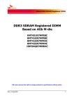
1
240pin DDR3 SDRAM Unbuffered DIMM
DDR3 SDRAM
Unbuffered DIMMs
Based on 4Gb A-Die
HMT425U6AFR6C
HMT451U6AFR8C
HMT451U7AFR8C
HMT41GU6AFR8C
HMT41GU7AFR8C
*SK hynix reserves the right to change products or specifications without notice.
Rev. 1.1 /Jul. 2013
1
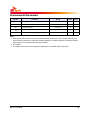
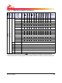
Revision History
Revision No.
History
Draft Date
0.1
Initial Release
Jul. 2012
0.2
JEDEC Spec Updated
Aug. 2012
1.0
Changed module maximum thickness
to reflect the measured maximum
May. 2013
1.1
Collected module dimension
Jul. 2013
Rev. 1.1 / Jul. 2013
Remark
2
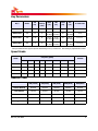
Description
SK hynix Unbuffered DDR3 SDRAM DIMMs (Unbuffered Double Data Rate Synchronous DRAM Dual In-Line
Memory Modules) are low power, high-speed operation memory modules that use DDR3 SDRAM devices.
These Unbuffered SDRAM DIMMs are intended for use as main memory when installed in systems such as
PCs and workstations.
Feature
• VDD=1.5V +/- 0.075V
• VDDQ=1.5V +/- 0.075V
• VDDSPD=3.0V to 3.6V
• 8 internal banks
• Data transfer rates: PC3-14900, PC3-12800, PC3-10600,PC3-8500
• Bi-directional Differential Data Strobe
• 8 bit pre-fetch
• Burst Length (BL) switch on-the-fly: BL 8 or BC (Burst Chop) 4
• Supports ECC error correction and detection
• On Die Termination (ODT) supported
• Temperature sensor with integrated SPD (Serial Presence Detect) EEPROM
• This product is in Compliance with the RoHS directive
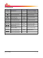
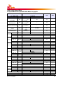
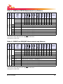
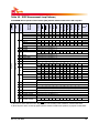
Ordering Information
Part Number
Density
Organization
Component Composition
# of
ranks
FDHS
HMT425U6AFR6C-G7/H9/PB/RD
2GB
256Mx64
256Mx16(H5TQ4G63AFR)*4
1
X
HMT451U6AFR8C-G7/H9/PB/RD
4GB
512Mx64
512Mx8(H5TQ4G83AFR)*8
1
X
HMT451U7AFR8C-G7/H9/PB/RD
4GB
512Mx72
512Mx8(H5TQ4G83AFR)*9
1
X
HMT41GU6AFR8C-G7/H9/PB/RD
8GB
1Gx64
512Mx8(H5TQ4G83AFR)*16
2
X
HMT41GU7AFR8C-G7/H9/PB/RD
8GB
1Gx72
512Mx8(H5TQ4G83MFR)*18
2
X
Rev. 1.1 / Jul. 2013
3
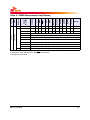
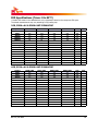
Key Parameters
MT/s
Grade
tCK
(ns)
CAS
Latency
(tCK)
tRCD
(ns)
tRP
(ns)
tRAS
(ns)
tRC
(ns)
CL-tRCD-tRP
DDR3-1066
-G7
1.875
7
13.125
13.125
37.5
50.625
7-7-7
DDR3-1333
-H9
1.5
9
13.5
13.5
(13.125)* (13.125)*
36
49.5
(49.125)*
9-9-9
DDR3-1600
-PB
1.25
11
13.75
13.75
(13.125)* (13.125)*
35
48.75
(48.125)*
11-11-11
DDR3-1866
-RD
1.07
13
13.91
13.91
(13.125)* (13.125)*
34
47.91
(47.125)*
13-13-13
*SK hynix DRAM devices support optional downbinning to CL11, CL9 and CL7. SPD setting is programmed to match.
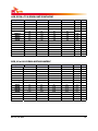
Speed Grade
Frequency [MHz]
Grade
Remark
CL6
CL7
CL8
CL9
CL10
-G7
800
1066
1066
-H9
800
1066
-PB
800
-RD
800
CL11
1066
1333
1333
1066
1066
1333
1333
1600
1066
1066
1333
1333
1600
CL12
CL13
1866
Address Table
2GB(1Rx16)
4GB(1Rx8)
4GB(1Rx8)
8GB(2Rx8)
8GB(2Rx8)
Refresh Method
8K/64ms
8K/64ms
8K/64ms
8K/64ms
8K/64ms
Row Address
A0-A14
A0-A15
A0-A15
A0-A15
A0-A15
Column Address
A0-A9
A0-A9
A0-A9
A0-A9
A0-A9
Bank Address
BA0-BA2
BA0-BA2
BA0-BA2
BA0-BA2
BA0-BA2
Page Size
2KB
1KB
1KB
1KB
1KB
Rev. 1.1 / Jul. 2013
4
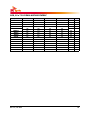
Pin Descriptions
Pin Name
Description
Pin Name
Description
I2C serial bus clock for EEPROM
A0–A15
SDRAM address bus
SCL
BA0–BA2
SDRAM bank select
SDA
I2C serial bus data line for EEPROM
SA0–SA2
I2C slave address select for EEPROM
RAS
SDRAM row address strobe
CAS
SDRAM column address strobe
WE
SDRAM write enable
VDDQ*
SDRAM I/O Driver power supply
DIMM Rank Select Lines
VREFDQ
SDRAM I/O reference supply
CKE0–CKE1
SDRAM clock enable lines
VREFCA
SDRAM command/address reference
supply
ODT0–ODT1
On-die termination control lines
S0–S1
DQ0–DQ63
CB0–CB7
DIMM memory data bus
DIMM ECC check bits
VDD*
VSS
VDDSPD
NC
SDRAM core power supply
Power supply return (ground)
Serial EEPROM positive power supply
Spare pins (no connect)
DQS0–DQS8
SDRAM data strobes
(positive line of differential pair)
TEST
Memory bus analysis tools
(unused on memory DIMMS)
DQS0–DQS8
SDRAM data strobes
(negative line of differential pair)
RESET
Set DRAMs to Known State
DM0–DM8
SDRAM data masks/high data strobes
(x8-based x72 DIMMs)
CK0–CK1
SDRAM clocks
(positive line of differential pair)
RSVD
CK0–CK1
SDRAM clocks
(negative line of differential pair)
-
VTT
SDRAM I/O termination supply
Reserved for future use
-
*The VDD and VDDQ pins are tied common to a single power-plane on these designs
Rev. 1.1 / Jul. 2013
5
Input/Output Functional Descriptions
Symbol
Type
Polarity
Function
CK0–CK1
CK0–CK1
SSTL
Differential
crossing
CK and CK are differential clock inputs. All the DDR3 SDRAM addr/cntl
inputs are sampled on the crossing of positive edge of CK and negative
edge of CK. Output (read) data is reference to the crossing of CK and CK
(Both directions of crossing).
CKE0–CKE1
SSTL
Active High
Activates the SDRAM CK signal when high and deactivates the CK signal
when low. By deactivating the clocks, CKE low initiates the Power Down
mode, or the Self Refresh mode.
S0–S1
SSTL
Active Low
Enables the associated SDRAM command decoder when low and disables
the command decoder when high. When the command decoder is disabled, new commands are ignored but previous operations continue. This
signal provides for external rank selection on systems with multiple ranks.
RAS, CAS, WE
SSTL
Active Low
RAS, CAS, and WE (ALONG WITH S) define the command being entered.
ODT0–ODT1
SSTL
Active High
When high, termination resistance is enabled for all DQ, DQS, DQS and DM
pins, assuming this function is enabled in the Mode Register 1 (MR1).
VREFDQ
Supply
Reference voltage for SSTL15 I/O inputs.
VREFCA
Supply
Reference voltage for SSTL 15 command/address inputs.
VDDQ
Supply
Power supply for the DDR3 SDRAM output buffers to provide improved
noise immunity. For all current DDR3 unbuffered DIMM designs, VDDQ
shares the same power plane as VDD pins.
BA0–BA2
SSTL
—
Selects which SDRAM bank of eight is activated.
During a Bank Activate command cycle, Address input defines the row
address (RA0–RA15).
A0–A15
SSTL
—
DQ0–DQ63,
CB0–CB7
SSTL
—
DM0–DM8
SSTL
VDD, VSS
Supply
Rev. 1.1 / Jul. 2013
Active High
During a Read or Write command cycle, Address input defines the column
address. In addition to the column address, AP is used to invoke autoprecharge operation at the end of the burst read or write cycle. If AP is high,
autoprecharge is selected and BA0, BA1, BA2 defines the bank to be precharged. If AP is low, autoprecharge is disabled. During a Precharge command cycle, AP is used in conjunction with BA0, BA1, BA2 to control which
bank(s) to precharge. If AP is high, all banks will be precharged regardless
of the state of BA0, BA1 or BA2. If AP is low, BA0, BA1 and BA2 are used to
define which bank to precharge. A12(BC) is sampled during READ and
WRITE commands to determine if burst chop (on-the-fly) will be performed (HIGH, no burst chop; LOW, burst chopped).
Data and Check Bit Input/Output pins.
DM is an input mask signal for write data. Input data is masked when DM
is sampled High coincident with that input data during a write access. DM
is sampled on both edges of DQS. Although DM pins are input only, the DM
loading matches the DQ and DQS loading.
Power and ground for the DDR3 SDRAM input buffers, and core logic. VDD
and VDDQ pins are tied to VDD/VDDQ planes on these modules.
6
Symbol
Type
Polarity
DQS0–DQS8
DQS0–DQS8
SSTL
Differential
crossing
Function
Data strobe for input and output data.
SA0–SA2
—
These signals are tied at the system planar to either VSS or VDDSPD to configure the serial SPD EEPROM address range.
SDA
—
This bidirectional pin is used to transfer data into or out of the SPD
EEPROM. An external resistor may be connected from the SDA bus line to
VDDSPD to act as a pullup on the system board.
SCL
—
This signal is used to clock data into and out of the SPD EEPROM. An
external resistor may be connected from the SCL bus time to VDDSPD to act
as a pullup on the system board.
VDDSPD
Supply
Rev. 1.1 / Jul. 2013
Power supply for SPD EEPROM. This supply is separate from the VDD/VDDQ
power plane. EEPROM supply is operable from 3.0V to 3.6V.
7
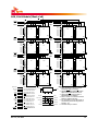
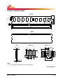
Pin Assignments
Front Side(left 1–60)
Pin
x64
# Non-ECC
x72
ECC
Back Side(right 121–180)
Front Side(left 61–120) Back Side(right 181–240)
Pin
x64
# Non-ECC
x72
ECC
Pin
#
x64
Non-ECC
x72
ECC
Pin
#
x64
Non-ECC
x72
ECC
VSS
VSS
61
A2
A2
181
A1
A1
1
VREFDQ
2
VSS
VSS
122
DQ4
DQ4
62
VDD
VDD
182
VDD
VDD
3
DQ0
DQ0
123
DQ5
DQ5
63
CK1
CK1
183
VDD
VDD
4
DQ1
DQ1
124
VSS
VSS
64
CK1
CK1
184
CK0
CK0
5
VSS
VSS
125
DM0
DM0
65
VDD
VDD
185
CK0
CK0
6
DQS0
DQS0
126
NC
NC
66
VDD
VDD
186
VDD
VDD
7
DQS0
DQS0
127
VSS
VSS
67
VREFCA
VREFCA
187
NC
EVENT
8
VSS
VSS
128
DQ6
DQ6
68
NC
NC
188
A0
A0
9
DQ2
DQ2
129
DQ7
DQ7
69
VDD
VDD
189
VDD
VDD
10
DQ3
DQ3
130
VSS
VSS
70
A10
A10
190
BA12
BA12
11
VSS
VSS
131
DQ12
DQ12
71
BA02
BA02
191
VDD
VDD
12
DQ8
DQ8
132
DQ13
DQ13
72
VDD
VDD
192
RAS
RAS
13
DQ9
DQ9
133
VSS
VSS
73
WE
WE
193
S0
S0
14
VSS
VSS
134
DM1
DM1
74
CAS
CAS
194
VDD
VDD
15
DQS1
DQS1
135
NC
NC
75
VDD
VDD
195
ODT0
ODT0
16
DQS1
DQS1
136
VSS
VSS
76
S1
S1
196
A13
A13
17
VSS
VSS
137
DQ14
DQ14
77
ODT1
ODT1
197
VDD
VDD
18
DQ10
DQ10
138
DQ15
DQ15
78
VDD
VDD
198
NC
NC
19
DQ11
DQ11
139
VSS
VSS
79
NC
NC
199
VSS
VSS
20
VSS
VSS
140
DQ20
DQ20
80
VSS
VSS
200
DQ36
DQ36
21
DQ16
DQ16
141
DQ21
DQ21
81
DQ32
DQ32
201
DQ37
DQ37
22
DQ17
DQ17
142
VSS
VSS
82
DQ33
DQ33
202
VSS
VSS
23
VSS
VSS
143
DM2
DM2
83
VSS
VSS
203
DM4
DM4
24
DQS2
DQS2
144
NC
NC
84
DQS4
DQS4
204
NC
NC
25
DQS2
DQS2
145
VSS
VSS
85
DQS4
DQS4
205
VSS
VSS
26
VSS
VSS
146
DQ22
DQ22
86
VSS
VSS
206
DQ38
DQ38
27
DQ18
DQ18
147
DQ23
DQ23
87
DQ34
DQ34
207
DQ39
DQ39
28
DQ19
DQ19
148
VSS
VSS
88
DQ35
DQ35
208
VSS
VSS
29
VSS
VSS
149
DQ28
DQ28
89
VSS
VSS
209
DQ44
DQ44
30
DQ24
DQ24
150
DQ29
DQ29
90
DQ40
DQ40
210
DQ45
DQ45
VREFDQ 121
NC = No Connect; RFU = Reserved Future Use
1. NC pins should not be connected to anything on the DIMM, including bussing within the NC group.
2. Address pins A3–A8 and BA0 and BA1 can be mirrored or not mirrored.
Rev. 1.1 / Jul. 2013
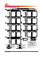
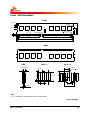
8
Front Side(left 1–60)
Back Side(right 121–180)
Front Side(left 61–120) Back Side(right 181–240)
x72
ECC
Pin
#
x64
Non-ECC
x72
ECC
Pin
#
x64
Non-ECC
x72
ECC
Pin
x64
# Non-ECC
x72
ECC
Pin
x64
# Non-ECC
31
DQ25
DQ25
151
VSS
VSS
91
DQ41
DQ41
211
VSS
VSS
32
VSS
VSS
152
DM3
DM3
92
VSS
VSS
212
DM5
DM5
33
DQS3
DQS3
153
NC
NC
93
DQS5
DQS5
213
NC
NC
34
DQS3
DQS3
154
VSS
VSS
94
DQS5
DQS5
214
VSS
VSS
35
VSS
VSS
155
DQ30
DQ30
95
VSS
VSS
215
DQ46
DQ46
36
DQ26
DQ26
156
DQ31
DQ31
96
DQ42
DQ42
216
DQ47
DQ47
37
DQ27
DQ27
157
VSS
VSS
97
DQ43
DQ43
217
VSS
VSS
38
VSS
VSS
158
NC
CB4
98
VSS
VSS
218
DQ52
DQ52
39
NC
CB0
159
NC
CB5
99
DQ48
DQ48
219
DQ53
DQ53
40
NC
CB1
160
VSS
VSS
100
DQ49
DQ49
220
VSS
VSS
41
VSS
VSS
161
DM8
DM8
101
VSS
VSS
221
DM6
DM6
42
NC
DQS8
162
NC
NC
102
DQS6
DQS6
222
NC
NC
43
NC
DQS8
163
VSS
VSS
103
DQS6
DQS6
223
VSS
VSS
44
VSS
VSS
164
NC
CB6
104
VSS
VSS
224
DQ54
DQ54
45
NC
CB2
165
NC
CB7
105
DQ50
DQ50
225
DQ55
DQ55
46
NC
CB3
166
VSS
VSS
106
DQ51
DQ51
226
VSS
VSS
47
VSS
VSS
167
NC
NC
107
VSS
VSS
227
DQ60
DQ60
48
NC
NC
168
Reset
Reset
108
DQ56
DQ56
228
DQ61
DQ61
109
DQ57
DQ57
229
VSS
VSS
KEY
KEY
49
NC
NC
169
CKE1/NC
CKE1/NC
110
VSS
VSS
230
DM7
DM7
50
CKE0
CKE0
170
VDD
VDD
111
DQS7
DQS7
231
NC
NC
51
VDD
VDD
171
NC
NC
112
DQS7
DQS7
232
VSS
VSS
52
BA2
BA2
172
A14
A14
113
VSS
VSS
233
DQ62
DQ62
53
NC
NC
173
VDD
VDD
114
DQ58
DQ58
234
DQ63
DQ63
54
VDD
VDD
174
A12
A12
115
DQ59
DQ59
235
VSS
VSS
55
All
All
175
A9
A9
116
VSS
VSS
236
VDDSPD
VDDSPD
56
A72
A72
176
VDD
VDD
117
SA0
SA0
237
SA1
SA1
57
VDD
VDD
177
A82
A82
118
SCL
SCL
238
SDA
SDA
58
A52
A52
178
A62
A62
119
SA2
SA2
239
VSS
VSS
59
A42
A42
179
VDD
VDD
120
VTT
VTT
240
VTT
VTT
60
VDD
VDD
180
A32
A32
NC = No Connect; RFU = Reserved Future Use
1. NC pins should not be connected to anything on the DIMM, including bussing within the NC group.
2. Address pins A3–A8 and BA0 and BA1 can be mirrored or not mirrored.
Rev. 1.1 / Jul. 2013
9
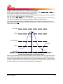
On DIMM Thermal Sensor
The DDR3 SDRAM DIMM temperature is monitored by integrated thermal sensor. The integrated thermal
sensor comply with JEDEC “TSE2002av, Serial Presence Detect with Temperature Sensor”.
Connection of Thermal Sensor
EVENT
SCL
SDA
SA0
EVENT
SPD with SA1
SCL Integrated
SA2
SDA
TS
SA0
SA1
SA2
Temperature-to-Digital Conversion Performance
Parameter
Temperature Sensor Accuracy (Grade B)
Resolution
Rev. 1.1 / Jul. 2013
Condition
Min
Typ
Max
Unit
Active Range,
75°C < TA < 95°C
-
± 0.5
± 1.0
°C
Monitor Range,
40°C < TA < 125°C
-
± 1.0
± 2.0
°C
-20°C < TA < 125°C
-
± 2.0
± 3.0
°C
0.25
°C
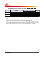
10
Functional Block Diagram
2GB, 256Mx64 Module(1Rank of x16)
S0
DQS0
DQS0
DM0
DQS1
DQS1
DM1
DQS2
DQS2
DM2
DQS3
DQS3
DM3
CS
DQ0
DQ1
DQ2
DQ3
DQ4
DQ5
DQ6
DQ7
LDQS
LDQS
LDM
I/O 0
I/O 1
I/O 2
I/O 3
I/O 4
I/O 5
I/O 6
I/O 7
DQ8
DQ9
DQ10
DQ11
DQ12
DQ13
DQ14
DQ15
UDQS
UDQS
UDM
I/O 8
I/O 9
I/O 10
I/O 11
I/O 12
I/O 13
I/O 14
I/O 15
DQ16
DQ17
DQ18
DQ19
DQ20
DQ21
DQ22
DQ23
LDQS
LDQS
LDM
I/O 0
I/O 1
I/O 2
I/O 3
I/O 4
I/O 5
I/O 6
I/O 7
DQ24
DQ25
DQ26
DQ27
DQ28
DQ29
DQ30
DQ31
UDQS
CS
UDQS
UDM
I/O 8
I/O 9
I/O 10
I/O 11
I/O 12
I/O 13
I/O 14
I/O 15
DQS4
DQS4
DM4
D0
DQS5
DQS5
DM5
ZQ
CS
DQS6
DQS6
DM6
CSD1
DQS7
DQS7
DM7
ZQ
DQ32
DQ33
DQ34
DQ35
DQ36
DQ37
DQ38
DQ39
DQ40
DQ41
DQ42
DQ43
DQ44
DQ45
DQ46
DQ47
UDQS
UDQS
UDM
I/O 8
I/O 9
I/O 10
I/O 11
I/O 12
I/O 13
I/O 14
I/O 15
DQ48
DQ49
DQ50
DQ51
DQ52
DQ53
DQ54
DQ55
LDQS
LDQS
LDM
I/O 0
I/O 1
I/O 2
I/O 3
I/O 4
I/O 5
I/O 6
I/O 7
DQ56
DQ57
DQ58
DQ59
DQ60
DQ61
DQ62
DQ63
UDQS
CS
UDQS
UDM
I/O 8
I/O 9
I/O 10
I/O 11
I/O 12
I/O 13
I/O 14
I/O 15
Serial PD
SCL
BA0–BA2
A0–A14
BA0–BA2: SDRAMs D0–D3
A0–A14: SDRAMs D0–D3
RAS
RAS: SDRAMs D0–D3
CAS
CAS: SDRAMs D0–D3
CKE0
CKE: SDRAMs D0–D3
WE
ODT0
WE: SDRAMs D0–D3
ODT: SDRAMs D0–D3
CK0
CK0
RESET
CK: SDRAMs D0–D3
CK: SDRAMs D0–D3
RESET:SDRAMs D0-D3
Rev. 1.1 / Jul. 2013
VDDSPD
SDA
WP
A0
A1
A2
SA0
SA1
SA2
CS
LDQS
LDQS
LDM
I/O 0
I/O 1
I/O 2
I/O 3
I/O 4
I/O 5
I/O 6
I/O 7
SPD
VDD/VDDQ
D0–D3
VREFDQ
D0–D3
VSS
D0–D3
VREFCA
D0–D3
D2
ZQ
CS
CSD3
ZQ
Notes:
1. DQ-to-I/O wiring is shown as recommended but may be changed.
2. DQ/DQS/DQS/ODT/DM/CKE/S relationships must be maintained as shown.
3. DQ,DM,DQS,DQS resistors;Refer to associated topology diagram.
4. Refer to the appropriate clock wiring
topology under the DIMM wiring details
section of this document.
5. The pair CK1 and CK1# is terminated in
75ohm but is not used on the module.
6. A15 is not routed on the module.
7. For each DRAM, a unique ZQ resistor is
connected to ground.The ZQ resistor is
240ohm+-1%
8. One SPD exists per module.
11
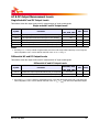
4GB, 512Mx64 Module(1Rank of x8)
S0
DQS0
DQS0
DM0
DQS1
DQS1
DM1
DQS2
DQS2
DM2
DQS3
DQS3
DM3
DQS4
DQS4
DM4
DM CS DQS DQS
0
1
D0
2
3
4
5
6
ZQ
7
DQ0
DQ1
DQ2
DQ3
DQ4
DQ5
DQ6
DQ7
I/O
I/O
I/O
I/O
I/O
I/O
I/O
I/O
DQ8
DQ9
DQ10
DQ11
DQ12
DQ13
DQ14
DQ15
DM CS DQS DQS
I/O 0
I/O 1
D1
I/O 2
I/O 3
I/O 4
I/O 5
ZQ
I/O 6
I/O 7
DQ16
DQ17
DQ18
DQ19
DQ20
DQ21
DQ22
DQ23
I/O
I/O
I/O
I/O
I/O
I/O
I/O
I/O
DQ24
DQ25
DQ26
DQ27
DQ28
DQ29
DM CS DQS DQS
I/O 0
I/O 1
D3
I/O 2
I/O 3
I/O 4
I/O 5
DQS5
DQS5
DM5
DQS6
DQS6
DM6
DM CS DQS DQS
0
1
D2
2
3
4
5
6
7
ZQ
DQS7
DQS7
DM7
DQ32
DQ33
DQ34
DQ35
DQ36
DQ37
DQ38
DQ39
DM
I/O 0
I/O 1
I/O 2
I/O 3
I/O 4
I/O 5
I/O 6
I/O 7
CS DQS DQS
DQ40
DQ41
DQ42
DQ43
DQ44
DQ45
DQ46
DQ47
DM
I/O 0
I/O 1
I/O 2
I/O 3
I/O 4
I/O 5
I/O 6
I/O 7
CS DQS DQS
DQ48
DQ49
DQ50
DQ51
DQ52
DQ53
DQ54
DQ55
DM
I/O 0
I/O 1
I/O 2
I/O 3
I/O 4
I/O 5
I/O 6
I/O 7
CS DQS DQS
DM
I/O 0
I/O 1
I/O 2
I/O 3
I/O 4
I/O 5
I/O 6
I/O 7
CS DQS DQS
DQ56
DQ57
DQ58
DQ59
DQ60
DQ61
Serial PD
SCL
BA0–BA2: SDRAMs D0–D7
A0–A15: SDRAMs D0–D7
RAS
RAS: SDRAMs D0–D7
CAS
CAS: SDRAMs D0–D7
CKE0
CKE: SDRAMs D0–D7
WE
ODT0
WE: SDRAMs D0–D7
CK0
CK0
CK: SDRAMs D0–D7
CK: SDRAMs D0–D7
RESET
ODT: SDRAMs D0–D7
RESET: SDRAMs D0-D7
Rev. 1.1 / Jul. 2013
VDDSPD
VDD/VDDQ
SDA
WP
A0
A1
A2
SA0
SA1
SA2
SPD
D0–D7
VREFDQ
D0–D7
VSS
D0–D7
VREFCA
D0–D7
D4
ZQ
D5
ZQ
D6
ZQ
D7
ZQ
Notes:
1. DQ-to-I/O wiring is shown as recommended but may be changed.
2. DQ/DQS/DQS/ODT/DM/CKE/S relationships must be maintained as shown.
3. DQ,DM,DQS/DQS resistors;Refer to
associated topology diagram.
4. Refer to the appropriate clock wiring
topology under the DIMM wiring details
section of this document.
5. Refer to Section 3.1 of this document for
details on address mirroring.
6. For each DRAM, a unique ZQ resistor is
connected to ground.The ZQ resistor is
240ohm+-1%
7. One SPD exists per module.
12
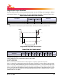
4GB, 512Mx72 Module(1Rank of x8)
S0
DQS0
DQS0
DM0
DQS1
DQS1
DM1
DQS2
DQS2
DM2
DQS3
DQS3
DM3
DQS8
DQS8
DM8
BA0–BA2
A0–A15
RAS
CAS
CKE0
WE
ODT0
CK0
CK0
RESET
DQS4
DQS4
DM4
DM
I/O 0
I/O 1
I/O 2
I/O 3
I/O 4
I/O 5
I/O 6
I/O 7
CS DQS DQS
DQ0
DQ1
DQ2
DQ3
DQ4
DQ5
DQ6
DQ7
DM
I/O 0
I/O 1
I/O 2
I/O 3
I/O 4
I/O 5
I/O 6
I/O 7
CS
DQ8
DQ9
DQ10
DQ11
DQ12
DQ13
DQ14
DQ15
DQ16
DQ17
DQ18
DQ19
DQ20
DQ21
DQ22
DQ23
DM
I/O 0
I/O 1
I/O 2
I/O 3
I/O 4
I/O 5
I/O 6
I/O 7
CS
DQ24
DQ25
DQ26
DQ27
DQ28
DQ29
DQ30
DQ31
DM
I/O 0
I/O 1
I/O 2
I/O 3
I/O 4
I/O 5
I/O 6
I/O 7
CS
CB0
CB1
CB2
CB3
CB4
CB5
CB6
CB7
DM
I/O 0
I/O 1
I/O 2
I/O 3
I/O 4
I/O 5
I/O 6
I/O 7
CS DQS DQS
D0
ZQ
DQS5
DQS5
DM5
DQS DQS
D1
ZQ
DQS6
DQS6
DM6
DQS DQS
D2
ZQ
DQS7
DQS7
DM7
DQS DQS
D3
ZQ
D8
DM
I/O 0
I/O 1
I/O 2
I/O 3
I/O 4
I/O 5
I/O 6
I/O 7
CS
DQ40
DQ41
DQ42
DQ43
DQ44
DQ45
DQ46
DQ47
DM
I/O 0
I/O 1
I/O 2
I/O 3
I/O 4
I/O 5
I/O 6
I/O 7
CS DQS DQS
DQ48
DQ49
DQ50
DQ51
DQ52
DQ53
DQ54
DQ55
DM
I/O 0
I/O 1
I/O 2
I/O 3
I/O 4
I/O 5
I/O 6
I/O 7
CS
DQ56
DQ57
DQ58
DQ59
DQ60
DQ61
DQ62
DQ63
DM
I/O 0
I/O 1
I/O 2
I/O 3
I/O 4
I/O 5
I/O 6
I/O 7
CS
SPD(TS integrated)
SCL
EVENT
ZQ
BA0–BA2: SDRAMs D0–D8
A0–A15: SDRAMs D0–D8 VDDSPD
RAS: SDRAMs D0–D8
VDD/VDDQ
CAS: SDRAMs D0–D8
CKE: SDRAMs D0–D8
VREFDQ
WE: SDRAMs D0–D8
VSS
ODT: SDRAMs D0–D8
CK: SDRAMs D0–D8
VREFCA
CK: SDRAMs D0–D8
RESET:SDRAMs D0-D8
Rev. 1.1 / Jul. 2013
DQ32
DQ33
DQ34
DQ35
DQ36
DQ37
DQ38
DQ39
EVENT
SDA
A0
A1
A2
SA0
SA1
SA2
SPD
D0–D8
D0–D8
D0–D8
D0–D8
DQS DQS
D4
ZQ
D5
ZQ
DQS DQS
D6
ZQ
DQS DQS
D7
ZQ
Notes:
1. DQ-to-I/O wiring is shown as recommended but may be changed.
2. DQ/DQS/DQS/ODT/DM/CKE/S relationships must be maintained as
shown.
3. DQ,CB,DM,DQS/DQS resistors;Refer
to associated topology diagram.
4. Refer to the appropriate clock wiring
topology under the DIMM wiring
details section of this document.
5. For each DRAM, a unique ZQ resistor
is connected to ground.The ZQ resistor is 240ohm+-1%
6. One SPD exists per module.
13
8GB, 1Gx64 Module(2Rank of x8)
S1
S0
DQS0
DQS0
DM0
DQS1
DQS1
DM1
DQS2
DQS2
DM2
DQS3
DQS3
DM3
DQS4
DQS4
DM4
DQ0
DQ1
DQ2
DQ3
DQ4
DQ5
DQ6
DQ7
DM
I/O 0
I/O 1
I/O 2
I/O 3
I/O 4
I/O 5
I/O 6
I/O 7
DM
I/O 0
I/O 1
I/O 2
I/O 3
I/O 4
I/O 5
I/O 6
I/O 7
CS DQS DQS
DQ8
DQ9
DQ10
DQ11
DQ12
DQ13
DQ14
DQ15
DM
I/O 0
I/O 1
I/O 2
I/O 3
I/O 4
I/O 5
I/O 6
I/O 7
CS DQS DQS
DQ16
DQ17
DQ18
DQ19
DQ20
DQ21
DQ22
DQ23
DQ24
DQ25
DQ26
DQ27
DQ28
DQ29
DQ30
DQ31
I/O 0
I/O 1
I/O 2
I/O 3
I/O 4
I/O 5
I/O 6
I/O 7
DM
CS DQS DQS
D0
ZQ
D1
ZQ
D2
ZQ
CS DQS DQS
D3
ZQ
DM CS DQS DQS
I/O 0
I/O 1
D8
I/O 2
I/O 3
I/O 4
I/O 5
I/O 6
ZQ
I/O 7
DM CS DQS DQS
I/O 0
I/O 1
D9
I/O 2
I/O 3
I/O 4
I/O 5
ZQ
I/O 6
I/O 7
DQS6
DQS6
DM6
DM CS DQS DQS
I/O 0
I/O 1
D10
I/O 2
I/O 3
I/O 4
I/O 5
ZQ
I/O 6
I/O 7
RESET
DM CS DQS DQS
I/O 0
I/O 1
D12
I/O 2
I/O 3
I/O 4
I/O 5
I/O 6
I/O 7
DQ40
DQ41
DQ42
DQ43
DQ44
DQ45
DQ46
DQ47
DM CS DQS DQS
I/O 0
I/O 1
D5
I/O 2
I/O 3
I/O 4
I/O 5
I/O 6
I/O 7
DM CS DQS DQS
I/O 0
I/O 1
D13
I/O 2
I/O 3
I/O 4
I/O 5
I/O 6
I/O 7
ZQ
DQ48
DQ49
DQ50
DQ51
DQ52
DQ53
DQ54
DQ55
DM CS DQS DQS
I/O 0
I/O 1
D6
I/O 2
I/O 3
I/O 4
I/O 5
I/O 6
I/O 7
DM CS DQS DQS
I/O 0
I/O 1
D14
I/O 2
I/O 3
I/O 4
I/O 5
I/O 6
I/O 7
ZQ
DQ56
DQ57
DQ58
DQ59
DQ60
DQ61
DQ62
DQ63
DM CS DQS DQS
I/O 0
I/O 1
D7
I/O 2
I/O 3
I/O 4
I/O 5
I/O 6
I/O 7
DM CS DQS DQS
I/O 0
I/O 1
D15
I/O 2
I/O 3
I/O 4
I/O 5
I/O 6
I/O 7
DQS7
DQS7
DM7
DM CS DQS DQS
I/O 0
I/O 1
D11
I/O 2
I/O 3
I/O 4
I/O 5
I/O 6
ZQ
I/O 7
BA0–BA2: SDRAMs D0–D15 SCL
A0-A15: SDRAMs D0–D15
WP
CKE: SDRAMs D8–D15
A0
CKE: SDRAMs D0–D7
SA0
RAS: SDRAMs D0–D15
CAS: SDRAMs D0–D15
VDDSPD
WE: SDRAMs D0–D15
VDD/VDDQ
ODT: SDRAMs D0–D7
VREFDQ
ODT: SDRAMs D8–D15
CK: SDRAMs D0–D7
CK: SDRAMs D0–D7
CK: SDRAMs D8–D15
CK: SDRAMs D8–D15
DM CS DQS DQS
I/O 0
I/O 1
D4
I/O 2
I/O 3
I/O 4
I/O 5
I/O 6
I/O 7
DQS5
DQS5
DM5
Serial PD
BA0–BA2
A0–A15
CKE1
CKE0
RAS
CAS
WE
ODT0
ODT1
CK0
CK0
CK1
CK1
DQ32
DQ33
DQ34
DQ35
DQ36
DQ37
DQ38
DQ39
VSS
VREFCA
A1
A2
SA1
SA2
ZQ
ZQ
ZQ
ZQ
ZQ
ZQ
Notes:
1. DQ-to-I/O wiring is shown as recomSDA
mended but may be changed.
2. DQ/DQS/DQS/ODT/DM/CKE/S relationships must be maintained as shown.
3. DQ,DM,DQS,DQS resistors;Refer to
associated topology diagram.
SPD
4. Refer to Section 3.1 of this document for
D0–D15
details on address mirroring.
5. For each DRAM, a unique ZQ resistor is
D0–D15
connected to ground.The ZQ resistor is
D0–D15
240ohm+-1%
6. One SPD exists per module.
D0–D15
RESET:SDRAMs D0-D3
Rev. 1.1 / Jul. 2013
14
8GB, 1Gx72 Module(2Rank of x8)
DQS1
DQS1
DM1
S1
S0
DQS0
DQS0
DM0
DQS4
DQS4
DM4
DQ0
DQ1
DQ2
DQ3
DQ4
DQ5
DQ6
DQ7
DM CS DQS DQS
I/O 0
I/O 1
D0
I/O 2
I/O 3
I/O 4
I/O 5
I/O 6
I/O 7
ZQ
DM
I/O 0
I/O 1
I/O 2
I/O 3
I/O 4
I/O 5
I/O 6
I/O 7
CS DQS DQS
DQ8
DQ9
DQ10
DQ11
DQ12
DQ13
DQ14
DQ15
I/O 0
I/O 1
I/O 2
I/O 3
I/O 4
I/O 5
I/O 6
I/O 7
DM
I/O 0
I/O 1
I/O 2
I/O 3
I/O 4
I/O 5
I/O 6
I/O 7
CS DQS DQS
DQ16
DQ17
DQ18
DQ19
DQ20
DQ21
DQ22
DQ23
DM CS DQS DQS
I/O 0
I/O 1
D2
I/O 2
I/O 3
I/O 4
I/O 5
I/O 6
I/O 7
ZQ
DM
I/O 0
I/O 1
I/O 2
I/O 3
I/O 4
I/O 5
I/O 6
I/O 7
CS DQS DQS
DQ24
DQ25
DQ26
DQ27
DQ28
DQ29
DQ30
DQ31
DM CS DQS DQS
I/O 0
I/O 1
D3
I/O 2
I/O 3
I/O 4
I/O 5
I/O 6
I/O 7
DM
I/O 0
I/O 1
I/O 2
I/O 3
I/O 4
I/O 5
I/O 6
I/O 7
DM
DQS2
DQS2
DM2
DQS3
DQS3
DM3
D1
ZQ
ZQ
DQS5
DQS5
DM5
D10
ZQ
DQS6
DQS6
DM6
D11
ZQ
DQS7
DQS7
DM7
ZQ
DQS8
DQS8
DM8
DM
I/O 0
I/O 1
I/O 2
I/O 3
I/O 4
I/O 5
I/O 6
I/O 7
DQ40
DQ41
DQ42
DQ43
DQ44
DQ45
DQ46
DQ47
DM CS DQS DQS
I/O 0
I/O 1
D5
I/O 2
I/O 3
I/O 4
I/O 5
I/O 6
I/O 7
DM
I/O 0
I/O 1
I/O 2
I/O 3
I/O 4
I/O 5
I/O 6
I/O 7
CS DQS DQS
DM CS DQS DQS
I/O 0
I/O 1
D6
I/O 2
I/O 3
I/O 4
I/O 5
I/O 6
I/O 7
ZQ
DM
I/O 0
I/O 1
I/O 2
I/O 3
I/O 4
I/O 5
I/O 6
I/O 7
CS DQS DQS
DQ48
DQ49
DQ50
DQ51
DQ52
DQ53
DQ54
DQ55
DQ56
DQ57
DQ58
DQ59
DQ60
DQ61
DQ62
DQ63
DM CS DQS DQS
I/O 0
I/O 1
D7
I/O 2
I/O 3
I/O 4
I/O 5
I/O 6
I/O 7
ZQ
DM
I/O 0
I/O 1
I/O 2
I/O 3
I/O 4
I/O 5
I/O 6
I/O 7
CS DQS DQS
CS DQS DQS
D12
ZQ
ZQ
ZQ
VDDSPD
SPD(TS integrated)
DM CS DQS DQS
I/O 0
I/O 1
D8
I/O 2
I/O 3
I/O 4
I/O 5
I/O 6
I/O 7
DM
I/O 0
I/O 1
I/O 2
I/O 3
I/O 4
I/O 5
I/O 6
I/O 7
ZQ
BA0-BA2: SDRAMs D0–D17
A0-A15: SDRAMs D0–D17
CKE: SDRAMs D0–D8
CKE: SDRAMs D9–D17
RAS: SDRAMs D0–D17
CAS: SDRAMs D0–D17
WE: SDRAMs D0–D17
Rev. 1.1 / Jul. 2013
CS DQS DQS
ODT0
ODT1
CK0
CK0
CK1
CK1
RESET
D17
EVENT
EVENT
A0
SA0
SA1
A2
SA2
ZQ
ODT: SDRAMs D0–D8
ODT: SDRAMs D9–D17
CK: SDRAMs D0–D8
CK: SDRAMs D0–D8
CK: SDRAMs D9–D17
CK: SDRAMs D9–D17
RESET:SDRAMs D0-D17
ZQ
D14
ZQ
D15
ZQ
D16
ZQ
SPD
D0–D17
VREFDQ
D0–D17
Vss
D0–D17
VREFCA
D0–D17
SDA
A1
D13
VDD/VDDQ
SCL
CB0
CB1
CB2
CB3
CB4
CB5
CB6
CB7
BA0–BA2
A0–A15
CKE0
CKE1
RAS
CAS
WE
CS DQS DQS
D9
DM CS DQS DQS
I/O 0
I/O 1
D4
I/O 2
I/O 3
I/O 4
I/O 5
I/O 6
I/O 7
CS DQS DQS
DQ32
DQ33
DQ34
DQ35
DQ36
DQ37
DQ38
DQ39
Notes:
1. DQ-to-I/O wiring is shown as recommended but may be changed.
2. DQ/DQS/DQS/ODT/DM/CKE/S relationships must be maintained as shown.
3. DQ,CB,DM/DQS/DQS resistors;Refer to
associated topology diagram.
4. Refer to Section 3.1 of this document for
details on address mirroring.
5. For each DRAM, a unique ZQ resistor is
connected to ground.The ZQ resistor is
240ohm+-1%
6. One SPD exists per module.
15
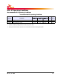
Absolute Maximum Ratings
Absolute Maximum DC Ratings
Absolute Maximum DC Ratings
Symbol
VDD
VDDQ
Parameter
Rating
Units
Notes
Voltage on VDD pin relative to Vss
- 0.4 V ~ 1.8 V
V
1, 3
Voltage on VDDQ pin relative to Vss
- 0.4 V ~ 1.8 V
V
1, 3
V
1
VIN, VOUT Voltage on any pin relative to Vss
TSTG
- 0.4 V ~ 1.8 V
-55 to +100
Storage Temperature
o
C
1, 2
Notes:
1. Stresses greater than those listed under “Absolute Maximum Ratings” may cause permanent damage to the
device. This is a stress rating only and functional operation of the device at these or any other conditions above
those indicated in the operational sections of this specification is not implied. Exposure to absolute maximum rating conditions for extended periods may affect reliability.
2. Storage Temperature is the case surface temperature on the center/top side of the DRAM. For the measurement
conditions, please refer to JESD51-2 standard.
3. VDD and VDDQ must be within 300mV of each other at all times; and VREF must not be greater than
0.6XVDDQ,When VDD and VDDQ are less than 500mV; VREF may be equal to or less than 300mV.
DRAM Component Operating Temperature Range
Temperature Range
Symbol
TOPER
Parameter
Normal Operating Temperature Range
Extended Temperature Range
Rating
Units
Notes
0 to 85
oC
1,2
85 to 95
oC
1,3
Notes:
1. Operating Temperature TOPER is the case surface temperature on the center / top side of the DRAM. For measurement conditions, please refer to the JEDEC document JESD51-2.
2. The Normal Temperature Range specifies the temperatures where all DRAM specifications will be supported. During operation, the DRAM case temperature must be maintained between 0 - 85oC under all operating conditions.
3. Some applications require operation of the DRAM in the Extended Temperature Range between 85oC and 95oC
case temperature. Full specifications are guaranteed in this range, but the following additional conditions apply:
a. Refresh commands must be doubled in frequency, therefore reducing the Refresh interval tREFI to 3.9 µs. It
is also possible to specify a component with 1X refresh (tREFI to 7.8µs) in the Extended Temperature Range.
Please refer to the DIMM SPD for option availability
b. If Self-Refresh operation is required in the Extended Temperature Range, then it is mandatory to use the
Manual Self-Refresh mode with Extended Temperature Range capability (MR2 A6 = 0b and MR2 A7 = 1b).
DDR3 SDRAMs support Extended Temperature Range and please refer to component datasheet and/or the
DIMM SPD for tFEFI requirements in the Extended Temperature Range.
Rev. 1.1 / Jul. 2013
16
AC & DC Operating Conditions
Recommended DC Operating Conditions
Recommended DC Operating Conditions
Symbol
VDD
VDDQ
Parameter
Rating
Units
Notes
1.575
V
1,2
1.575
V
1,2
Min.
Typ.
Max.
Supply Voltage
1.425
1.500
Supply Voltage for Output
1.425
1.500
Notes:
1. Under all conditions, VDDQ must be less than or equal to VDD.
2. VDDQ tracks with VDD. AC parameters are measured with VDD and VDDQ tied together.
Rev. 1.1 / Jul. 2013
17
AC & DC Input Measurement Levels
AC and DC Logic Input Levels for Single-Ended Signals
AC and DC Input Levels for Single-Ended Command and Address Signals
Single Ended AC and DC Input Levels for Command and ADDress
Symbol
VIH.CA(DC100)
VIL.CA(DC100)
VIH.CA(AC175)
VIL.CA(AC175)
VIH.CA(AC150)
VIL.CA(AC150)
VIH.CA(AC135)
VIL.CA(AC135)
VIH.CA(AC125)
VIL.CA(AC125)
VRefCA(DC)
Parameter
DDR3-800/1066/1333/1600
Min
DC input logic high
Vref + 0.100
DC input logic low
VSS
AC input logic high
Vref + 0.175
AC input logic low
Note2
AC Input logic high
Vref + 0.150
AC input logic low
Note2
AC input logic high
AC input logic low
AC Input logic high
AC input logic low
Reference Voltage for
0.49 * VDD
ADD, CMD inputs
DDR3-1866
Unit
Notes
VDD
Vref - 0.100
Note2
Vref - 0.135
Note2
Vref - 0.125
V
V
V
V
V
V
V
V
mV
mV
1, 5
1, 6
1, 2, 7
1, 2, 8
1, 2, 7
1, 2, 8
1, 2, 7
1, 2, 8
1, 2, 7
1, 2, 8
0.51 * VDD
V
3, 4
Max
Min
Max
VDD
Vref - 0.100
Note2
Vref - 0.175
Note2
Vref - 0.150
-
Vref + 0.100
VSS
Vref + 0.135
Note2
Vref + 0.125
Note2
0.51 * VDD
0.49 * VDD
Notes:
1. For input only pins except RESET, Vref = VrefCA (DC).
2. Refer to "Overshoot and Undershoot Specifications" on page 31.
3. The ac peak noise on VRef may not allow VRef to deviate from VRefCA(DC) by more than +/-1% VDD (for
ence: approx. +/- 15 mV).
refer-
4. For reference: approx. VDD/2 +/- 15 mV.
5. VIH(dc) is used as a simplified symbol for VIH.CA(DC100)
6. VIL(dc) is used as a simplified symbol for VIL.CA(DC100)
7. VIH(ac) is used as simplified symbol for VIH.CA(AC175), VIH.CA(AC150), VIH.CA(AC135), and VIH.CA(AC125);
VIH.CA(AC175) value is used when Vref + 0.175V is referenced, VIH.CA(AC150) value is used when Vref +
0.150V is referenced, VIH.CA(AC135) value is used when Vref + 0.135V is referenced, and VIH.CA(AC125) value
is used when Vref + 0.125V is referenced.
8. VIL(ac) is used as simplified symbol for VIL.CA(AC175), VIL.CA(AC150), VIL.CA(AC135), and VIL.CA(AC125);
VIL.CA(AC175) value is used when Vref - 0.175V is referenced, VIL.CA(AC150) value is used when Vref - 0.150V is
referenced, VIL.CA(AC135) value is used when Vref - 0.135V is referenced, and VIL.CA(AC125) value is used
when Vref - 0.125V is referenced.
Rev. 1.1 / Jul. 2013
18
AC and DC Input Levels for Single-Ended Signals
DDR3 SDRAM will support two Vih/Vil AC levels for DDR3-800 and DDR3-1066 as specified in the table
below. DDR3 SDRAM will also support corresponding tDS values (Table 43 and Table 51 in “ DDR3 Device
Operation”) as well as derating tables in Table 46 of “DDR3 Device Operation” depending on Vih/Vil AC levels.
Single Ended AC and DC Input Levels for DQ and DM
Symbol
Parameter
VIH.DQ(DC100)
VIL.DQ(DC100)
VIH.DQ(AC175)
VIL.DQ(AC175)
VIH.DQ(AC150)
VIL.DQ(AC150)
VIH.CA(AC135)
VIL.CA(AC135)
DC input logic high
DC input logic low
AC input logic high
AC input logic low
AC Input logic high
AC input logic low
AC input logic high
AC input logic low
Reference Voltage
for DQ, DM inputs
VRefDQ(DC)
DDR3-800/1066
DDR3-1333/1600
Min
Min
Max
Max
DDR3-1866
Min
Max
Unit Notes
Vref + 0.100
VDD
Vref + 0.100
VDD
Vref + 0.100
VDD
V
1, 5
VSS
Vref - 0.100
VSS
Vref - 0.100
VSS
Vref - 0.100 V
1, 6
Vref + 0.175 Note2
V 1, 2, 7
Note2
Vref - 0.175
V 1, 2, 8
Vref + 0.150 Note2 Vref + 0.150 Note2 Vref + 0.150 Note2
V 1, 2, 7
Note2
Vref - 0.150
Note2
Vref - 0.150
Note2
Vref - 0.150 V 1, 2, 8
Vref + 0.135 Note2
mV 1, 2, 7
Note2
Vref - 0.135 mV 1, 2, 8
0.49 * VDD 0.51 * VDD 0.49 * VDD 0.51 * VDD 0.49 * VDD 0.51 * VDD
V
Notes:
1. Vref = VrefDQ (DC).
2. Refer to "Overshoot and Undershoot Specifications" on page 31.
3. The ac peak noise on VRef may not allow VRef to deviate from VRefDQ(DC) by more than +/-1% VDD (for reference:
approx. +/- 15 mV).
4. For reference: approx. VDD/2 +/- 15 mV.
5. VIH(dc) is used as a simplified symbol for VIH.DQ(DC100)
6. VIL(dc) is used as a simplified symbol for VIL.DQ(DC100)
7. VIH(ac) is used as simplified symbol for VIH.DQ(AC175), VIH.DQ(AC150), and VIH.DQ(AC135); VIH.DQ(AC175)
value is used when Vref + 0.175V is referenced, VIH.DQ(AC150) value is used when Vref + 0.150V is referenced,
and VIH.DQ(AC135) value is used when Vref + 0.135V is referenced.
8. VIL(ac) is used as simplified symbol for VIL.DQ(AC175), VIL.DQ(AC150), and VIL.DQ(AC135); VIL.DQ(AC175)
value is used when Vref - 0.175V is referenced, VIL.DQ(AC150) value is used when Vref - 0.150V is referenced,
and VIL.DQ(AC135) value is used when Vref - 0.135V is referenced.
Rev. 1.1 / Jul. 2013
19
3, 4
Vref Tolerances
The dc-tolerance limits and ac-noise limits for the reference voltages VRefCA and VRefDQ are illustrated in
figure below. It shows a valid reference voltage VRef (t) as a function of time. (VRef stands for VRefCA and
VRefDQ likewise).
VRef (DC) is the linear average of VRef (t) over a very long period of time (e.g. 1 sec). This average has to
meet the min/max requirements in the table "Differential AC and DC Input Levels" on page 22. Furthermore VRef (t) may temporarily deviate from VRef (DC) by no more than +/- 1% VDD.
voltage
VDD
VRef ac-noise
VRef(DC)
VRef(t)
VRef(DC)max
VDD/2
VRef(DC)min
VSS
time
Illustration of VRef(DC) tolerance and VRef ac-noise limits
The voltage levels for setup and hold time measurements VIH(AC), VIH(DC), VIL(AC), and VIL(DC) are dependent on VRef.
“VRef ” shall be understood as VRef(DC), as defined in figure above.
This clarifies that dc-variations of VRef affect the absolute voltage a signal has to reach to achieve a valid
high or low level and therefore the time to which setup and hold is measured. System timing and voltage
budgets need to account for VRef(DC) deviations from the optimum position within the data-eye of the input
signals.
This also clarifies that the DRAM setup/hold specification and derating values need to include time and
voltage associated with VRefac-noise. Timing and voltage effects due to ac-noise on VRef up to the specified limit (+/- 1% of VDD) are included in DRAM timings and their associated deratings.
Rev. 1.1 / Jul. 2013
20
AC and DC Logic Input Levels for Differential Signals
Differential signal definition
tDVAC
Differential Input Voltage(i.e.DQS - DQS#, CK - CK#)
VIL.DIFF.AC.MIN
VIL.DIFF.MIN
0
half cycle
VIL.DIFF.MAX
VIL.DIFF.AC.MAX
tDVAC
time
Definition of differential ac-swing and “time above ac-level” tDVAC
Rev. 1.1 / Jul. 2013
21
Differential swing requirements for clock (CK - CK) and strobe (DQS-DQS)
Differential AC and DC Input Levels
DDR3-800, 1066, 1333, 1600, 1866
Symbol
Parameter
VIHdiff
VILdiff
VIHdiff (ac)
VILdiff (ac)
Differential input high
Differential input logic low
Differential input high ac
Differential input low ac
Min
Max
+ 0.180
Note 3
2 x (VIH (ac) - Vref)
Note 3
Note 3
- 0.180
Note 3
2 x (VIL (ac) - Vref)
Unit Notes
V
V
V
V
1
1
2
2
Notes:
1. Used to define a differential signal slew-rate.
2. For CK - CK use VIH/VIL (ac) of AADD/CMD and VREFCA; for DQS - DQS, DQSL, DQSL, DQSU, DQSU use VIH/VIL
(ac) of DQs and VREFDQ; if a reduced ac-high or ac-low levels is used for a signal group, then the reduced level
applies also here.
3. These values are not defined; however, the single-ended signals Ck, CK, DQS, DQS, DQSL, DQSL, DQSU, DQSU
need to be within the respective limits (VIH (dc) max, VIL (dc) min) for single-ended signals as well as the limitations for overshoot and undershoot. Refer to "Overshoot and Undershoot Specifications" on page 31.
Allowed time before ringback (tDVAC) for CK - CK and DQS - DQS
DDR3-800/1066/1333/1600
Slew
Rate
[V/ns]
tDVAC [ps]
@ VIH/Ldiff (ac)
= 350mV
tDVAC [ps]
@ VIH/Ldiff (ac)
= 300mV
DDR3-1866
tDVAC [ps]
@ VIH/Ldiff (ac)
tDVAC [ps]
tDVAC [ps]
= 270mV
@ VIH/Ldiff (ac)| @ VIH/Ldiff (ac)|
(DQS-DQS)only
= 300mV
= (CK-CK)only
(Optional)
min
max
min
max
min
max
min
max
min
max
> 4.0
75
-
175
-
214
-
134
-
139
-
4.0
57
-
170
-
214
-
134
-
139
-
3.0
50
-
167
-
191
-
112
-
118
-
2.0
38
-
119
1.8
34
-
102
-
131
-
52
-
63
-
1.6
29
-
81
-
113
-
33
-
45
-
1.4
22
-
54
-
88
-
9
-
23
-
1.2
13
-
19
-
56
-
note
-
note
-
1.0
0
-
note
-
11
-
note
-
note
-
< 1.0
0
-
note
-
note
-
note
-
note
-
146
67
77
note : Rising input differential signal shall become equal to or greater than VIHdiff(ac) level and Falling
input differential signal shall become equal to or less than VIL(ac) level.
Rev. 1.1 / Jul. 2013
22
Single-ended requirements for differential signals
Each individual component of a differential signal (CK, DQS, DQSL, DQSU, CK, DQS, DQSL, of DQSU) also
has to comply with certain requirements for single-ended signals.
CK and CK have to approximately reach VSEHmin / VSELmax (approximately equal to the ac-levels (VIH
(ac) / VIL (ac)) for ADD/CMD signals) in every half-cycle.
DQS, DQSL, DQSU, DQS, DQSL have to reach VSEHmin / VSELmax (approximately the ac-levels (VIH (ac)
/ VIL (ac)) for DQ signals) in every half-cycle preceding and following a valid transition.
Note that the applicable ac-levels for ADD/CMD and DQ’s might be different per speed-bin etc. E.g., if
VIH.CA(AC150)/VIL.CA(AC150) is used for ADD/CMD signals, then these ac-levels apply also for the singleended signals CK and CK.
VDD or VDDQ
VSEHmin
VSEH
VDD/2 or VDDQ/2
CK or DQS
VSELmax
VSS or VSSQ
VSEL
time
Single-ended requirements for differential signals.
Note that, while ADD/CMD and DQ signal requirements are with respect to Vref, the single-ended components of differential signals have a requirement with respect to VDD / 2; this is nominally the same. the
transition of single-ended signals through the ac-levels is used to measure setup time. For single-ended
components of differential signals the requirement to reach VSELmax, VSEHmin has no bearing on timing,
but adds a restriction on the common mode characteristics of these signals.
Rev. 1.1 / Jul. 2013
23
Single-ended levels for CK, DQS, DQSL, DQSU, CK, DQS, DQSL or DQSU
Symbol
VSEH
VSEL
Parameter
Single-ended high level for strobes
Single-ended high level for Ck, CK
Single-ended low level for strobes
Single-ended low level for CK, CK
DDR3-800, 1066, 1333, & 1600
Min
Max
(VDD / 2) + 0.175
(VDD /2) + 0.175
Note 3
Note 3
Note 3
Note 3
(VDD / 2) - 0.175
(VDD / 2) - 0.175
Unit Notes
V
V
V
V
1,2
1,2
1,2
1,2
Notes:
1. For CK, CK use VIH/VIL (ac) of ADD/CMD; for strobes (DQS, DQS, DQSL, DQSL, DQSU, DQSU) use VIH/VIL (ac)
of DQs.
2. VIH (ac)/VIL (ac) for DQs is based on VREFDQ; VIH (ac)/VIL (ac) for ADD/CMD is based on VREFCA; if a reduced
ac-high or ac-low level is used for a signal group, then the reduced level applies also here.
3. These values are not defined; however, the single-ended signals Ck, CK, DQS, DQS, DQSL, DQSL, DQSU, DQSU
need to be within the respective limits (VIH (dc) max, VIL (dc) min) for single-ended signals as well as the limitations for overshoot and undershoot. Refer to "Overshoot and Undershoot Specifications" on page 31.
Rev. 1.1 / Jul. 2013
24
Differential Input Cross Point Voltage
To guarantee tight setup and hold times as well as output skew parameters with respect to clock and
strobe, each cross point voltage of differential input signals (CK, CK and DQS, DQS) must meet the
requirements in table below. The differential input cross point voltage VIX is measured from the actual
cross point of true and complement signals to the midlevel between of VDD and VSS
Vix Definition
Cross point voltage for differential input signals (CK, DQS)
Symbol
Parameter
VIX(CK)
VIX(DQS)
DDR3-800, 1066, 1333, 1600, 1866
Unit Notes
Min
Max
Differential Input Cross Point Voltage
relative to VDD/2 for CK, CK
-150
-175
150
175
mV
mV
2
1
Differential Input Cross Point Voltage
relative to VDD/2 for DQS, DQS
-150
150
mV
2
Notes:
1. Extended range for VIX is only allowed for clock and if single-ended clock input signals CK and CK are monotonic
with a single-ended swing VSEL / VSEH of at least VDD/2 +/-250 mV, and when the differential slew rate of CK CK is larger than 3 V/ns.
2. The relation between Vix Min/Max and VSEL/VSEH should satisfy following.
(VDD/2) + Vix (Min) - VSEL 25mV
VSEH - ((VDD/2) + Vix (Max)) 25mV
Rev. 1.1 / Jul. 2013
25
Slew Rate Definitions for Single-Ended Input Signals
See 7.5 “Address / Command Setup, Hold and Derating” in “DDR3 Device Operation” for single-ended slew
rate definitions for address and command signals.
See 7.6 “Data Setup, Hold and Slew Rate Derating” in “DDR3 Device Operation” for single-ended slew rate
definition for data signals.
Slew Rate Definitions for Differential Input Signals
Input slew rate for differential signals (CK, CK and DQS, DQS) are defined and measured as shown in table
and figure below.
Differential Input Slew Rate Definition
Measured
Description
Differential input slew rate for rising edge
(CK-CK and DQS-DQS)
Differential input slew rate for falling edge
(CK-CK and DQS-DQS)
Defined by
Min
Max
VILdiffmax
VIHdiffmin
[VIHdiffmin-VILdiffmax] / DeltaTRdiff
VIHdiffmin
VILdiffmax
[VIHdiffmin-VILdiffmax] / DeltaTFdiff
Notes:
Differential Input Voltage (i.e. DQS-DQS; CK-CK)
The differential signal (i.e. CK-CK and DQS-DQS) must be linear between these thresholds.
Delta
TRdiff
VIHdiffmin
0
VILdiffmax
Delta
TFdiff
Differential Input Slew Rate Definition for DQS, DQS and CK, CK
Rev. 1.1 / Jul. 2013
26
AC & DC Output Measurement Levels
Single Ended AC and DC Output Levels
Table below shows the output levels used for measurements of single ended signals.
Single-ended AC and DC Output Levels
Symbol
Parameter
VOH(DC)
DC output high measurement level (for IV curve linearity)
VOM(DC)
DC output mid measurement level (for IV curve linearity)
VOL(DC)
DC output low measurement level (for IV curve linearity)
VOH(AC)
AC output high measurement level (for output SR)
VOL(AC)
AC output low measurement level (for output SR)
DDR3-800, 1066,
1333, 1600, 1866
0.8 x VDDQ
Unit
Notes
V
0.5 x VDDQ
0.2 x VDDQ
V
VTT + 0.1 x VDDQ
VTT - 0.1 x VDDQ
V
1
V
1
V
Notes:
1. The swing of ±0.1 x VDDQ is based on approximately 50% of the static single ended output high or low swing with
a driver impedance of 40 Ω and an effective test load of 25 Ω to VTT = VDDQ / 2.
Differential AC and DC Output Levels
Table below shows the output levels used for measurements of single ended signals.
Differential AC and DC Output Levels
Symbol
VOHdiff (AC)
VOLdiff (AC)
Parameter
DDR3-800, 1066,
1333, 1600, 1866
+ 0.2 x VDDQ
AC differential output high measurement level (for output SR)
- 0.2 x VDDQ
AC differential output low measurement level (for output SR)
Unit
Notes
V
1
V
1
Notes:
1. The swing of ±0.2 x VDDQ is based on approximately 50% of the static differential output high or low swing with
a driver impedance of 40 Ω and an effective test load of 25 Ω to VTT = VDDQ/2 at each of the differential outputs.
Rev. 1.1 / Jul. 2013
27
Single Ended Output Slew Rate
When the Reference load for timing measurements, output slew rate for falling and rising edges is defined
and measured between VOL(AC) and VOH(AC) for single ended signals are shown in table and figure below.
Single-ended Output slew Rate Definition
Measured
Description
Defined by
From
To
Single-ended output slew rate for rising edge
VOL(AC)
VOH(AC)
[VOH(AC)-VOL(AC)] / DeltaTRse
Single-ended output slew rate for falling edge
VOH(AC)
VOL(AC)
[VOH(AC)-VOL(AC)] / DeltaTFse
Notes:
1. Output slew rate is verified by design and characterisation, and may not be subject to production test.
Single Ended Output Voltage(l.e.DQ)
Delta TRse
VOH(AC)
V∏
VOl(AC)
Delta TFse
Single Ended Output slew Rate Definition
Output Slew Rate (single-ended)
DDR3-800 DDR3-1066 DDR3-1333 DDR3-1600 DDR3-1866
Parameter
Symbol
Min
Max
Min
Max
Min
Max
Min
Max
Min
Max
Single-ended Output Slew Rate
SRQse
2.5
5
2.5
5
2.5
5
2.5
5
2.5
51)
Units
V/ns
Description: SR; Slew Rate
Q: Query Output (like in DQ, which stands for Data-in, Query-Output)
se: Single-ended Signals
For Ron = RZQ/7 setting
Note 1): In two cases, a maximum slew rate of 6V/ns applies for a single DQ signal within a byte lane.
Case 1 is a defined for a single DQ signal within a byte lane which is switching into a certain direction (either from high
to low or low to high) while all remaining DQ signals in the same byte lane are static (i.e. they stay at either high or low).
Case 2 is a defined for a single DQ signal within a byte lane which is switching into a certain direction (either from high
to low or low to high) while all remaining DQ signals in the same byte lane switching into the opposite direction (i.e. from
low to high of high to low respectively). For the remaining DQ signal switching in to the opposite direction, the regular
maximum limite of 5 V/ns applies.
Rev. 1.1 / Jul. 2013
28
Differential Output Slew Rate
With the reference load for timing measurements, output slew rate for falling and rising edges is defined
and measured between VOLdiff (AC) and VOHdiff (AC) for differential signals as shown in table and figure
below.
Differential Output Slew Rate Definition
Measured
Description
Defined by
From
To
Differential output slew rate for rising edge
VOLdiff (AC)
VOHdiff (AC)
[VOHdiff (AC)-VOLdiff (AC)] / DeltaTRdiff
Differential output slew rate for falling edge
VOHdiff (AC)
VOLdiff (AC)
[VOHdiff (AC)-VOLdiff (AC)] / DeltaTFdiff
Notes:
1. Output slew rate is verified by design and characterization, and may not be subject to production test.
Differential Output Voltage(i.e. DQS-DQS)
Delta
TRdiff
VOHdiff(AC)
O
VOLdiff(AC)
Delta
TFdiff
Differential Output slew Rate Definition
Differential Output Slew Rate
DDR3-800
Parameter
Symbol Min
Max
DDR3-1066 DDR3-1333 DDR3-1600 DDR3-1866
Min
Max
Min
Differential Output Slew Rate SRQdiff
5
10
5
10
5
Description: SR; Slew Rate
Q: Query Output (like in DQ, which stands for Data-in, Query-Output)
se: Single-ended Signals
For Ron = RZQ/7 setting
Rev. 1.1 / Jul. 2013
Max
Min
Max
Min
Max
10
5
10
5
12
Units
V/ns
29
Reference Load for AC Timing and Output Slew Rate
Figure Below represents the effective reference load of 25 ohms used in defining the relevant AC timing
parameters of the device as well as output slew rate measurements.
It is not intended as a precise representation of any particular system environment or a depiction of the
actual load presented by a production tester. System designers should use IBIS or other simulation tools to
correlate the timing reference load to a system environment. Manufacturers correlate to their production
test conditions, generally one or more coaxial transmission lines terminated at the tester electronics.
VDDQ
CK, CK
DUT
DQ
DQS
DQS
25 Ohm
VTT = VDDQ/2
Reference Load for AC Timing and Output Slew Rate
Rev. 1.1 / Jul. 2013
30
Overshoot and Undershoot Specifications
Address and Control Overshoot and Undershoot Specifications
AC Overshoot/Undershoot Specification for Address and Control Pins
DDR3- DDR3- DDR3- DDR3- DDR3-
Parameter
800
Maximum peak amplitude allowed for overshoot area. (See Figure below)
0.4
Maximum peak amplitude allowed for undershoot area. (See Figure below) 0.4
Maximum overshoot area above VDD (See Figure below)
0.67
Maximum undershoot area below VSS (See Figure below)
0.67
(A0-A15, BA0-BA3, CS, RAS, CAS, WE, CKE, ODT)
See figure below for each parameter definition
1066 1333
0.4
0.4
0.5
0.5
0.4
0.4
0.4
0.4
1600 1866
0.4
0.4
0.33
0.33
Units
0.4
V
0.4
V
0.28 V-ns
0.28 V-ns
Maximum Amplitude
Overshoot Area
Volts
(V)
VDD
VSS
Undershoot Area
Maximum Amplitude
Time (ns)
Address and Control Overshoot and Undershoot Definition
Rev. 1.1 / Jul. 2013
31
Clock, Data, Strobe and Mask Overshoot and Undershoot Specifications
AC Overshoot/Undershoot Specification for Clock, Data, Strobe and Mask
DDR3- DDR3- DDR3- DDR3- DDR3-
Parameter
800
Maximum peak amplitude allowed for overshoot area. (See Figure below)
0.4
Maximum peak amplitude allowed for undershoot area. (See Figure below)
0.4
Maximum overshoot area above VDD (See Figure below)
0.25
Maximum undershoot area below VSS (See Figure below)
0.25
(CK, CK, DQ, DQS, DQS, DM)
See figure below for each parameter definition
1066 1333 1600 1866
0.4
0.4
0.19
0.19
0.4
0.4
0.15
0.15
0.4
0.4
0.13
0.13
Units
0.4
V
0.4
V
0.11 V-ns
0.11 V-ns
Maximum Amplitude
Overshoot Area
Volts
(V)
VDDQ
VSSQ
Undershoot Area
Maximum Amplitude
Time (ns)
Clock, Data, Strobe and Mask Overshoot and Undershoot Definition
Rev. 1.1 / Jul. 2013
32
Refresh parameters by device density
Refresh parameters by device density
Parameter
REF command ACT or
REF command time
Average periodic
refresh interval
RTT_Nom Setting
512Mb
1Gb
2Gb
4Gb
8Gb
tRFC
90
110
160
260
350
ns
7.8
7.8
7.8
7.8
7.8
us
3.9
3.9
3.9
3.9
3.9
us
tREFI
0 C TCASE 85 C
85 C TCASE 95 C
Units Notes
Notes:
1. Users should refer to the DRAM supplier data sheet and/or the DIMM SPD to determine if DDR3 SDRAM devices
support the following options or requirements referred to in this materia.
Rev. 1.1 / Jul. 2013
33
Standard Speed Bins
DDR3 SDRAM Standard Speed Bins include tCK, tRCD, tRP, tRAS and tRC for each corresponding bin.
DDR3-800 Speed Bins
For specific Notes See "Speed Bin Table Notes" on page 39.
Speed Bin
DDR3-800E
CL - nRCD - nRP
6-6-6
Unit
Parameter
Symbol
min
max
Internal read command to first data
tAA
15
20
ns
ACT to internal read or write delay time
tRCD
15
—
ns
PRE command period
tRP
15
—
ns
ACT to ACT or REF command period
tRC
52.5
—
ns
ACT to PRE command period
tRAS
37.5
9 * tREFI
ns
tCK(AVG)
2.5
3.3
ns
CL = 6
CWL = 5
Supported CL Settings
6
nCK
Supported CWL Settings
5
nCK
Rev. 1.1 / Jul. 2013
Notes
1, 2, 3
34
DDR3-1066 Speed Bins
For specific Notes See "Speed Bin Table Notes" on page 39.
Speed Bin
DDR3-1066F
CL - nRCD - nRP
Parameter
Symbol
Unit
7-7-7
min
max
Note
Internal read command to
first data
tAA
13.125
20
ns
ACT to internal read or
write delay time
tRCD
13.125
—
ns
PRE command period
tRP
13.125
—
ns
ACT to ACT or REF
command period
tRC
50.625
—
ns
ACT to PRE command
period
tRAS
37.5
9 * tREFI
ns
CWL = 5
tCK(AVG)
2.5
3.3
ns
1, 2, 3, 6
CWL = 6
tCK(AVG)
Reserved
ns
1, 2, 3, 4
CWL = 5
tCK(AVG)
Reserved
ns
4
CWL = 6
tCK(AVG)
ns
1, 2, 3, 4
CWL = 5
tCK(AVG)
ns
4
CWL = 6
tCK(AVG)
ns
1, 2, 3
CL = 6
CL = 7
CL = 8
1.875
< 2.5
Reserved
1.875
< 2.5
Supported CL Settings
6, 7, 8
nCK
Supported CWL Settings
5, 6
nCK
Rev. 1.1 / Jul. 2013
35
DDR3-1333 Speed Bins
For specific Notes See "Speed Bin Table Notes" on page 39.
Speed Bin
DDR3-1333H
CL - nRCD - nRP
Parameter
Symbol
min
Internal read command
to first data
tAA
ACT to internal read or
write delay time
tRCD
13.5
(13.125)5,10
13.5
(13.125)5,10
PRE command period
tRP
ACT to ACT or REF
command period
ACT to PRE command
period
CL = 6
CL = 7
CL = 8
CL = 9
Unit
9-9-9
Note
max
20
ns
—
ns
13.5
(13.125)5,10
—
ns
tRC
49.5
(49.125)5,10
—
ns
tRAS
36
9 * tREFI
ns
CWL = 5
tCK(AVG)
2.5
3.3
ns
1, 2, 3, 7
CWL = 6
tCK(AVG)
Reserved
ns
1, 2, 3, 4, 7
CWL = 7
tCK(AVG)
Reserved
ns
4
CWL = 5
tCK(AVG)
Reserved
ns
4
CWL = 6
tCK(AVG)
ns
1, 2, 3, 4, 7
CWL = 7
tCK(AVG)
Reserved
ns
1, 2, 3, 4
CWL = 5
tCK(AVG)
Reserved
ns
4
CWL = 6
tCK(AVG)
ns
1, 2, 3, 7
CWL = 7
tCK(AVG)
Reserved
ns
1, 2, 3, 4
CWL = 5, 6
tCK(AVG)
Reserved
ns
4
CWL = 7
tCK(AVG)
ns
1, 2, 3, 4
CWL = 5, 6
tCK(AVG)
1.875
< 2.5
(Optional)5,10
1.875
< 2.5
1.5
<1.875
ns
4
1, 2, 3
(Optional)
ns
ns
Supported CL Settings
6, (7), 8, 9, (10)
nCK
Supported CWL Settings
5, 6, 7
nCK
CL = 10
CWL = 7
Rev. 1.1 / Jul. 2013
tCK(AVG)
Reserved
1.5
<1.875
36
DDR3-1600 Speed Bins
For specific Notes See "Speed Bin Table Notes" on page 39.
Speed Bin
CL - nRCD - nRP
Parameter
DDR3-1600K
Unit
11-11-11
Note
Symbol
min
max
Internal read command to first
data
tAA
13.75
(13.125)5,10
20
ns
ACT to internal read or write
delay time
tRCD
13.75
(13.125)5,10
—
ns
PRE command period
tRP
13.75
(13.125)5,10
—
ns
ACT to ACT or REF command
period
tRC
48.75
(48.125)5,10
—
ns
ACT to PRE command period
tRAS
35
9 * tREFI
ns
tCK(AVG)
tCK(AVG)
tCK(AVG)
tCK(AVG)
2.5
3.3
ns
1, 2, 3, 8
Reserved
ns
1, 2, 3, 4, 8
Reserved
ns
4
ns
4
ns
1, 2, 3, 4, 8
ns
1, 2, 3, 4, 8
CWL = 5
CWL = 6
CL = 6
CWL = 7
CWL = 5
CL = 7
CWL = 6
tCK(AVG)
CWL = 7
tCK(AVG)
tCK(AVG)
tCK(AVG)
tCK(AVG)
tCK(AVG)
tCK(AVG)
tCK(AVG)
CWL = 8
CWL = 5
CWL = 6
CL = 8
CWL = 7
CWL = 8
CWL = 5, 6
CL = 9
CWL = 7
tCK(AVG)
CWL = 8
tCK(AVG)
tCK(AVG)
tCK(AVG)
tCK(AVG)
tCK(AVG)
tCK(AVG)
CWL = 5, 6
CL = 10
CWL = 7
CWL = 8
CL = 11
CWL = 5, 6,7
CWL = 8
Reserved
1.875
< 2.5
(Optional)5,10
Reserved
Reserved
Reserved
1.875
< 2.5
Reserved
Reserved
Reserved
1.5
<1.875
(Optional)5,10
Reserved
Reserved
1.5
<1.875
Reserved
Reserved
1.25
<1.5
Supported CL Settings
6, (7), 8, (9), 10, 11
Supported CWL Settings
5, 6, 7, 8
Rev. 1.1 / Jul. 2013
ns
4
ns
4
ns
1, 2, 3, 8
ns
1, 2, 3, 4, 8
ns
1, 2, 3, 4
ns
4
ns
1, 2, 3, 4, 8
ns
1, 2, 3, 4
ns
4
ns
1, 2, 3, 8
ns
1,2,3,4
ns
4
ns
nCK
nCK
1, 2, 3
37
DDR3-1866 Speed Bins
For specific Notes See "Speed Bin Table Notes" on page 39.
Speed Bin
DDR3-1866M
CL - nRCD - nRP
Parameter
Symbol
Unit
13-13-13
Internal read command
to first data
tAA
min
13.91
(13.125)5,11
ACT to internal read or
write delay time
tRCD
PRE command period
Note
max
20
ns
13.91
(13.125)5,11
—
ns
tRP
13.91
(13.125)5,11
—
ns
ACT to PRE command
period
tRAS
34
9 * tREFI
ns
ACT to ACT or PRE
command period
tRC
47.91
(47.125)5,11
-
ns
2.5
3.3
ns
1, 2, 3, 9
Reserved
ns
1, 2, 3, 4, 9
Reserved
Reserved
ns
ns
4
4
ns
1, 2, 3, 4, 9
Reserved
ns
4
Reserved
ns
ns
4
1, 2, 3, 9
Reserved
ns
1, 2, 3, 4, 9
Reserved
ns
4
ns
4
ns
1, 2, 3, 4, 9
Reserved
ns
1, 2, 3, 4, 9
Reserved
ns
4
ns
ns
4
1, 2, 3, 9
ns
1, 2, 3, 4, 9
ns
4
ns
1, 2, 3, 4, 9
CWL = 7,8,9
CWL = 5
tCK(AVG)
tCK(AVG)
tCK(AVG)
tCK(AVG)
CWL = 6
tCK(AVG)
CWL = 7,8,9
tCK(AVG)
tCK(AVG)
tCK(AVG)
tCK(AVG)
tCK(AVG)
tCK(AVG)
CWL = 5
CL = 6
CL = 7
CL = 8
CWL = 6
CWL = 5
CWL = 6
CWL = 7
CWL = 8,9
CWL = 5, 6
CL = 9
CWL = 7
tCK(AVG)
CWL = 8
tCK(AVG)
tCK(AVG)
tCK(AVG)
tCK(AVG)
tCK(AVG)
tCK(AVG)
CWL = 9
CL = 10
CWL = 5, 6
CWL = 7
CWL = 8
CWL = 5,6,7
CL = 11
CWL = 8
tCK(AVG)
1.875
< 2.5
(Optinal)
1.875
< 2.5
Reserved
1.5
<1.875
(Optinal)
Reserved
1.5
<1.875
Reserved
Reserved
1.25
<1.5
(Optinal)
tCK(AVG)
CWL = 9
CWL = 5,6,7,8 tCK(AVG)
Reserved
ns
1, 2, 3, 4
Reserved
ns
4
tCK(AVG)
CWL = 9
CWL = 5,6,7,8 tCK(AVG)
CL = 13
tCK(AVG)
CWL = 9
Reserved
ns
1,2,3,4
Reserved
ns
ns
4
1, 2, 3
CL = 12
1.07
<1.25
Supported CL Settings
6, 7, 8, 9, 10, 11, 13
Supported CWL Settings
5, 6, 7, 8, 9
Rev. 1.1 / Jul. 2013
nCK
nCK
38
Speed Bin Table Notes
Absolute Specification (TOPER; VDDQ = VDD = 1.5V +/- 0.075 V);
1. The CL setting and CWL setting result in tCK(AVG).MIN and tCK(AVG).MAX requirements. When making a selection of tCK(AVG), both need to be fulfilled: Requirements from CL setting as well as requirements from CWL setting.
2. tCK(AVG).MIN limits: Since CAS Latency is not purely analog - data and strobe output are synchronized by the DLL - all possible intermediate frequencies may not be guaranteed. An application should
use the next smaller JEDEC standard tCK(AVG) value (3.0, 2.5, 1.875, 1.5, or 1.25 ns) when calculating CL [nCK] = tAA [ns] / tCK(AVG) [ns], rounding up to the next ‘Supported CL’, where tCK(AVG) =
3.0 ns should only be used for CL = 5 calculation.
3. tCK(AVG).MAX limits: Calculate tCK(AVG) = tAA.MAX / CL SELECTED and round the resulting tCK(AVG)
down to the next valid speed bin (i.e. 3.3ns or 2.5ns or 1.875 ns or 1.25 ns). This result is
tCK(AVG).MAX corresponding to CL SELECTED.
4. ‘Reserved’ settings are not allowed. User must program a different value.
5. ‘Optional’ settings allow certain devices in the industry to support this setting, however, it is not a mandatory feature. Refer to DIMM data sheet and/or the DIMM SPD information if and how this setting is
supported.
6. Any DDR3-1066 speed bin also supports functional operation at lower frequencies as shown in the
table which are not subject to Production Tests but verified by Design/Characterization.
7. Any DDR3-1333 speed bin also supports functional operation at lower frequencies as shown in the
table which are not subject to Production Tests but verified by Design/Characterization.
8. Any DDR3-1600 speed bin also supports functional operation at lower frequencies as shown in the
table which are not subject to Production Tests but verified by Design/Characterization.
9. Any DDR3-1866 speed bin also supports functional operation at lower frequencies as shown in the
table which are not subject to Production Tests but verified by Design/Characterization.
10. DDR3 SDRAM devices supporting optional down binning to CL=7 and CL=9, and tAA/tRCD/tRP must
be 13.125 ns or lower. SPD settings must be programmed to match. For example, DDR3-1333H
devices supporting down binning to DDR3-1066F should program 13.125 ns in SPD bytes for tAAmin
(Byte 16), tRCDmin (Byte 18), and tRPmin (Byte 20). DDR3-1600K devices supporting down binning to
DDR3-1333H or DDR3-1600F should program 13.125 ns in SPD bytes for tAAmin (Byte 16), tRCDmin
(Byte 18), and tRPmin (Byte 20). Once tRP (Byte 20) is programmed to 13.125ns, tRCmin (Byte 21,23)
also should be programmed accordingly. For example, 49.125ns (tRASmin + tRPmin = 36 ns + 13.125
ns) for DDR3-1333H and 48.125ns (tRASmin + tRPmin = 35 ns + 13.125 ns) for DDR3-1600K.
11. DDR3 SDRAM devices supporting optional down binning to CL=11, CL=9 and CL=7, tAA/tRCD/tRPmin must be
13.125ns. SPD setting must be programed to match. For example, DDR3-1866 devices supporting down binning
to DDR3-1600 or DDR3-1333 or 1066 should program 13.125ns in SPD bytes for tAAmin(byte 16), tRCDmin(byte
18) and tRPmin(byte 20) is programmed to 13.125ns, tRCmin(byte 21,23) also should be programmed accordingly. For example, 47.125ns (tRASmin + tRPmin = 34ns + 13.125ns)
Rev. 1.1 / Jul. 2013
39
Environmental Parameters
Symbol
Parameter
Rating
Units
TOPR
Operating temperature (ambient)
0 to +55
o
HOPR
Operating humidity (relative)
10 to 90
%
TSTG
Storage temperature
HSTG
Storage humidity (without condensation)
PBAR
Barometric Pressure (operating & storage)
o
-50 to +100
C
Notes
3
C
1
5 to 95
%
1
105 to 69
K Pascal
1, 2
Note:
1. Stress greater than those listed may cause permanent damage to the device. This is a stress rating only, and
device functional operation at or above the conditions indicated is not implied. Expousure to absolute maximum
rating conditions for extended periods may affect reliablility.
2. Up to 9850 ft.
3. The designer must meet the case temperature specifications for individual module components.
Rev. 1.1 / Jul. 2013
40
IDD and IDDQ Specification Parameters and Test Conditions
IDD and IDDQ Measurement Conditions
In this chapter, IDD and IDDQ measurement conditions such as test load and patterns are defined. Figure
below (Measurement Setup and Test Load for IDD and IDDQ (optional) Measurements) shows the setup
and test load for IDD and IDDQ measurements.
•
IDD currents (such as IDD0, IDD1, IDD2N, IDD2NT, IDD2P0, IDD2P1, IDD2Q, IDD3N, IDD3P, IDD4R,
IDD4W, IDD5B, IDD6, IDD6ET and IDD7) are measured as time-averaged currents with all VDD balls
of the DDR3 SDRAM under test tied together. Any IDDQ current is not included in IDD currents.
•
IDDQ currents (such as IDDQ2NT and IDDQ4R) are measured as time-averaged currents with all
VDDQ balls of the DDR3 SDRAM under test tied together. Any IDD current is not included in IDDQ currents.
Attention: IDDQ values cannot be directly used to calculate IO power of the DDR3 SDRAM. They can
be used to support correlation of simulated IO power to actual IO power as outlined in the Figure
below (Correlation from simulated Channel IO Power to actual Channel IO Power supported by IDDQ
Measurement). In DRAM module application, IDDQ cannot be measured separately since VDD and
VDDQ are using on merged-power layer in Module PCB.
For IDD and IDDQ measurements, the following definitions apply:
•
”0” and “LOW” is defined as VIN <= VILAC(max).
•
”1” and “HIGH” is defined as VIN >= VIHAC(max).
•
“MID_LEVEL” is defined as inputs are VREF = VDD/2.
•
Timing used for IDD and IDDQ Measurement-Loop Patterns are provided in Table 1.
•
Basic IDD and IDDQ Measurement Conditions are described in Table 2.
•
Detailed IDD and IDDQ Measurement-Loop Patterns are described in Table 3 through Table 10.
•
IDD Measurements are done after properly initializing the DDR3 SDRAM. This includes but is not limited to setting
RON = RZQ/7 (34 Ohm in MR1);
Qoff = 0B (Output Buffer enabled in MR1);
RTT_Nom = RZQ/6 (40 Ohm in MR1);
RTT_Wr = RZQ/2 (120 Ohm in MR2);
TDQS Feature disabled in MR1
•
Attention: The IDD and IDDQ Measurement-Loop Patterns need to be executed at least one time
before actual IDD or IDDQ measurement is started.
•
Define D = {CS, RAS, CAS, WE}:= {HIGH, LOW, LOW, LOW}
•
Define D = {CS, RAS, CAS, WE}:= {HIGH, HIGH, HIGH, HIGH}
Rev. 1.1 / Jul. 2013
41
IDDQ (optional)
IDD
VDD
VDDQ
RESET
CK/CK
DDR3
SDRAM
CKE
CS
RAS, CAS, WE
DQS, DQS
DQ, DM,
TDQS, TDQS
A, BA
ODT
ZQ
VSS
RTT = 25 Ohm
VDDQ/2
VSSQ
Measurement Setup and Test Load for IDD and IDDQ (optional) Measurements
[Note: DIMM level Output test load condition may be different from above
Application specific
memory channel
environment
IDDQ
Test Load
Channel
IO Power
Simulation
IDDQ
Simulation
IDDQ
Simulation
Correction
Channel IO Power
Number
Correlation from simulated Channel IO Power to actual Channel IO Power supported
by IDDQ Measurement
Rev. 1.1 / Jul. 2013
42
Table 1 -Timings used for IDD and IDDQ Measurement-Loop Patterns
Symbol
tCK
DDR3-1066
DDR3-1333
DDR3-1600
DDR3-1866
7-7-7
9-9-9
11-11-11
13-13-13
1.875
1.5
1.25
1.07
Unit
ns
CL
7
9
11
13
nCK
nRCD
7
9
11
13
nCK
nRC
27
33
39
45
nCK
nRAS
20
24
28
32
nCK
nRP
7
9
11
13
nCK
1KB page size
20
20
24
26
nCK
2KB page size
27
30
32
33
nCK
1KB page size
4
4
5
5
nCK
nFAW
nRRD
6
5
6
6
nCK
nRFC -512Mb
2KB page size
48
60
72
85
nCK
nRFC-1 Gb
59
74
88
103
nCK
nRFC- 2 Gb
86
107
128
150
nCK
nRFC- 4 Gb
139
174
208
243
nCK
nRFC- 8 Gb
187
234
280
328
nCK
Table 2 -Basic IDD and IDDQ Measurement Conditions
Symbol
Description
Operating One Bank Active-Precharge Current
CKE: High; External clock: On; tCK, nRC, nRAS, CL: see Table 1; BL: 8a); AL: 0; CS: High between ACT and
IDD0
PRE; Command, Address, Bank Address Inputs: partially toggling according to Table 3; Data IO: MID-LEVEL;
DM: stable at 0; Bank Activity: Cycling with one bank active at a time: 0,0,1,1,2,2,... (see Table 3); Output Buffer and RTT: Enabled in Mode Registersb); ODT Signal: stable at 0; Pattern Details: see Table 3.
Operating One Bank Active-Precharge Current
CKE: High; External clock: On; tCK, nRC, nRAS, nRCD, CL: see Table 1; BL: 8a); AL: 0; CS: High between ACT,
IDD1
RD and PRE; Command, Address; Bank Address Inputs, Data IO: partially toggling according to Table 4; DM:
stable at 0; Bank Activity: Cycling with on bank active at a time: 0,0,1,1,2,2,... (see Table 4); Output Buffer and
RTT: Enabled in Mode Registersb); ODT Signal: stable at 0; Pattern Details: see Table 4.
Rev. 1.1 / Jul. 2013
43
Symbol
Description
Precharge Standby Current
CKE: High; External clock: On; tCK, CL: see Table 1; BL: 8a); AL: 0; CS: stable at 1; Command, Address, Bank
IDD2N
Address Inputs: partially toggling according to Table 5; Data IO: MID_LEVEL; DM: stable at 0; Bank Activity: all
banks closed; Output Buffer and RTT: Enabled in Mode Registersb); ODT Signal: stable at 0; Pattern Details:
see Table 5.
Precharge Standby ODT Current
CKE: High; External clock: On; tCK, CL: see Table 1; BL: 8a); AL: 0; CS: stable at 1; Command, Address, Bank
IDD2NT Address Inputs: partially toggling according to Table 6; Data IO: MID_LEVEL; DM: stable at 0; Bank Activity: all
banks closed; Output Buffer and RTT: Enabled in Mode Registersb); ODT Signal: toggling according to Table 6;
Pattern Details: see Table 6.
Precharge Power-Down Current Slow Exit
IDD2P0
CKE: Low; External clock: On; tCK, CL: see Table 1; BL: 8a); AL: 0; CS: stable at 1; Command, Address, Bank
Address Inputs: stable at 0; Data IO: MID_LEVEL; DM: stable at 0; Bank Activity: all banks closed; Output Buffer and RTT: Enabled in Mode Registersb); ODT Signal: stable at 0; Precharge Power Down Mode: Slow Exitc)
Precharge Power-Down Current Fast Exit
IDD2P1
CKE: Low; External clock: On; tCK, CL: see Table 1; BL: 8a); AL: 0; CS: stable at 1; Command, Address, Bank
Address Inputs: stable at 0; Data IO: MID_LEVEL; DM: stable at 0; Bank Activity: all banks closed; Output Buffer and RTT: Enabled in Mode Registersb); ODT Signal: stable at 0; Precharge Power Down Mode: Fast Exitc)
Precharge Quiet Standby Current
IDD2Q
CKE: High; External clock: On; tCK, CL: see Table 1; BL: 8a); AL: 0; CS: stable at 1; Command, Address, Bank
Address Inputs: stable at 0; Data IO: MID_LEVEL; DM: stable at 0; Bank Activity: all banks closed; Output Buffer and RTT: Enabled in Mode Registersb); ODT Signal: stable at 0
Active Standby Current
CKE: High; External clock: On; tCK, CL: see Table 1; BL: 8a); AL: 0; CS: stable at 1; Command, Address, Bank
IDD3N
Address Inputs: partially toggling according to Table 5; Data IO: MID_LEVEL; DM: stable at 0; Bank Activity: all
banks open; Output Buffer and RTT: Enabled in Mode Registersb); ODT Signal: stable at 0; Pattern Details: see
Table 5.
Active Power-Down Current
IDD3P
CKE: Low; External clock: On; tCK, CL: see Table 1; BL: 8a); AL: 0; CS: stable at 1; Command, Address, Bank
Address Inputs: stable at 0; Data IO: MID_LEVEL; DM: stable at 0; Bank Activity: all banks open; Output Buffer
and RTT: Enabled in Mode Registersb); ODT Signal: stable at 0
Rev. 1.1 / Jul. 2013
44
Symbol
Description
Operating Burst Read Current
CKE: High; External clock: On; tCK, CL: see Table 1; BL: 8a); AL: 0; CS: High between RD; Command, Address,
IDD4R
Bank Address Inputs: partially toggling according to Table 7; Data IO: seamless read data burst with different
data between one burst and the next one according to Table 7; DM: stable at 0; Bank Activity: all banks open,
RD commands cycling through banks: 0,0,1,1,2,2,...(see Table 7); Output Buffer and RTT: Enabled in Mode
Registersb); ODT Signal: stable at 0; Pattern Details: see Table 7.
Operating Burst Write Current
CKE: High; External clock: On; tCK, CL: see Table 1; BL: 8a); AL: 0; CS: High between WR; Command, Address,
IDD4W
Bank Address Inputs: partially toggling according to Table 8; Data IO: seamless read data burst with different
data between one burst and the next one according to Table 8; DM: stable at 0; Bank Activity: all banks open,
WR commands cycling through banks: 0,0,1,1,2,2,...(see Table 8); Output Buffer and RTT: Enabled in Mode
Registersb); ODT Signal: stable at HIGH; Pattern Details: see Table 8.
Burst Refresh Current
CKE: High; External clock: On; tCK, CL, nRFC: see Table 1; BL: 8a); AL: 0; CS: High between REF; Command,
IDD5B
Address, Bank Address Inputs: partially toggling according to Table 9; Data IO: MID_LEVEL; DM: stable at 0;
Bank Activity: REF command every nREF (see Table 9); Output Buffer and RTT: Enabled in Mode Registersb);
ODT Signal: stable at 0; Pattern Details: see Table 9.
Self-Refresh Current: Normal Temperature Range
TCASE: 0 - 85 oC; Auto Self-Refresh (ASR): Disabledd);Self-Refresh Temperature Range (SRT): Normale); CKE:
IDD6
Low; External clock: Off; CK and CK: LOW; CL: see Table 1; BL: 8a); AL: 0; CS, Command, Address, Bank
Address Inputs, Data IO: MID_LEVEL; DM: stable at 0; Bank Activity: Self-Refresh operation; Output Buffer
and RTT: Enabled in Mode Registersb); ODT Signal: MID_LEVEL
Self-Refresh Current: Extended Temperature Range
TCASE: 0 - 95 oC; Auto Self-Refresh (ASR): Disabledd);Self-Refresh Temperature Range (SRT): Extendede);
IDD6ET
CKE: Low; External clock: Off; CK and CK: LOW; CL: see Table 1; BL: 8a); AL: 0; CS, Command, Address, Bank
Address Inputs, Data IO: MID_LEVEL; DM: stable at 0; Bank Activity: Extended Temperature Self-Refresh
operation; Output Buffer and RTT: Enabled in Mode Registersb); ODT Signal: MID_LEVEL
Rev. 1.1 / Jul. 2013
45
Symbol
Description
Operating Bank Interleave Read Current
CKE: High; External clock: On; tCK, nRC, nRAS, nRCD, NRRD, nFAW, CL: see Table 1; BL: 8a),f); AL: CL-1; CS:
High between ACT and RDA; Command, Address, Bank Address Inputs: partially toggling according to Table
IDD7
10; Data IO: read data burst with different data between one burst and the next one according to Table 10;
DM: stable at 0; Bank Activity: two times interleaved cycling through banks (0, 1,...7) with different addressing, wee Table 10; Output Buffer and RTT: Enabled in Mode Registersb); ODT Signal: stable at 0; Pattern
Details: see Table 10.
a) Burst Length: BL8 fixed by MRS: set MR0 A[1,0]=00B
b) Output Buffer Enable: set MR1 A[12] = 0B; set MR1 A[5,1] = 01B; RTT_Nom enable: set MR1 A[9,6,2] = 011B;
RTT_Wr enable: set MR2 A[10,9] = 10B
c) Precharge Power Down Mode: set MR0 A12=0B for Slow Exit or MR0 A12 = 1B for Fast Exit
d) Auto Self-Refresh (ASR): set MR2 A6 = 0B to disable
e) Self-Refresh Temperature Range (SRT): set MR2 A7 = 0B for normal or 1B for extended temperature range
f) Read Burst Type: Nibble Sequential, set MR0 A[3] = 0B
Rev. 1.1 / Jul. 2013
46
Command
CS
RAS
CAS
WE
ODT
BA[2:0]
A[15:11]
A[10]
A[9:7]
A[6:3]
A[2:0]
0
ACT
0
0
1
1
0
0
00
0
0
0
0
-
1,2
D, D
1
0
0
0
0
0
00
0
0
0
0
-
D, D
1
1
1
1
0
0
00
0
0
0
0
-
0
0
0
-
0
F
0
-
Cycle
Number
Datab)
Sub-Loop
CKE
CK, CK
Table 3 - IDD0 Measurement-Loop Patterna)
0
3,4
...
nRAS
...
Static High
toggling
1*nRC+0
repeat pattern 1...4 until nRAS - 1, truncate if necessary
PRE
0
0
1
0
0
0
00
0
repeat pattern 1...4 until nRC - 1, truncate if necessary
ACT
0
0
1
1
0
0
00
0
1*nRC+1, 2
D, D
1
0
0
0
0
0
00
0
0
F
0
-
1*nRC+3, 4
D, D
1
1
1
1
0
0
00
0
0
F
0
-
0
-
...
1*nRC+nRAS
repeat pattern 1...4 until 1*nRC + nRAS - 1, truncate if necessary
PRE
0
0
1
0
0
0
00
0
0
...
repeat pattern 1...4 until 2*nRC - 1, truncate if necessary
1
2*nRC
repeat Sub-Loop 0, use BA[2:0] = 1 instead
2
4*nRC
repeat Sub-Loop 0, use BA[2:0] = 2 instead
3
6*nRC
repeat Sub-Loop 0, use BA[2:0] = 3 instead
4
8*nRC
repeat Sub-Loop 0, use BA[2:0] = 4 instead
5
10*nRC
repeat Sub-Loop 0, use BA[2:0] = 5 instead
6
12*nRC
repeat Sub-Loop 0, use BA[2:0] = 6 instead
7
14*nRC
repeat Sub-Loop 0, use BA[2:0] = 7 instead
F
a) DM must be driven LOW all the time. DQS, DQS are MID-LEVEL.
b) DQ signals are MID-LEVEL.
Rev. 1.1 / Jul. 2013
47
Command
CS
RAS
CAS
WE
ODT
BA[2:0]
A[15:11]
A[10]
A[9:7]
A[6:3]
A[2:0]
0
ACT
0
0
1
1
0
0
00
0
0
0
0
-
1,2
D, D
1
0
0
0
0
0
00
0
0
0
0
-
D, D
1
1
1
1
0
0
00
0
0
0
0
-
0
0
00000000
0
0
0
-
Cycle
Number
Datab)
Sub-Loop
CKE
CK, CK
Table 4 - IDD1 Measurement-Loop Patterna)
0
3,4
...
nRCD
...
nRAS
Static High
toggling
...
repeat pattern 1...4 until nRCD - 1, truncate if necessary
RD
0
1
0
1
0
0
00
0
0
repeat pattern 1...4 until nRAS - 1, truncate if necessary
PRE
0
0
1
0
0
0
00
0
repeat pattern 1...4 until nRC - 1, truncate if necessary
1*nRC+0
ACT
0
0
1
1
0
0
00
0
0
F
0
-
1*nRC+1,2
D, D
1
0
0
0
0
0
00
0
0
F
0
-
D, D
1
1
1
1
0
0
00
0
0
F
0
-
1*nRC+3,4
...
1*nRC+nRCD
...
1*nRC+nRAS
repeat pattern nRC + 1,...4 until nRC + nRCE - 1, truncate if necessary
RD
0
1
0
1
0
0
00
0
0
F
0
00110011
repeat pattern nRC + 1,...4 until nRC + nRAS - 1, truncate if necessary
PRE
0
0
1
0
0
0
00
0
0
F
...
repeat pattern nRC + 1,...4 until *2 nRC - 1, truncate if necessary
1
2*nRC
repeat Sub-Loop 0, use BA[2:0] = 1 instead
2
4*nRC
repeat Sub-Loop 0, use BA[2:0] = 2 instead
3
6*nRC
repeat Sub-Loop 0, use BA[2:0] = 3 instead
4
8*nRC
repeat Sub-Loop 0, use BA[2:0] = 4 instead
5
10*nRC
repeat Sub-Loop 0, use BA[2:0] = 5 instead
6
12*nRC
repeat Sub-Loop 0, use BA[2:0] = 6 instead
7
14*nRC
repeat Sub-Loop 0, use BA[2:0] = 7 instead
0
-
a) DM must be driven LOW all the time. DQS, DQS are used according to RD Commands, otherwise MID-LEVEL.
b) Burst Sequence driven on each DQ signal by Read Command. Outside burst operation, DQ signals are MID_LEVEL.
Rev. 1.1 / Jul. 2013
48
Static High
CS
RAS
CAS
WE
ODT
BA[2:0]
A[15:11]
A[10]
A[9:7]
A[6:3]
A[2:0]
0
D
1
0
0
0
0
0
0
0
0
0
0
-
1
D
1
0
0
0
0
0
0
0
0
0
0
-
2
D
1
1
1
1
0
0
0
0
0
F
0
-
3
D
1
1
1
1
0
0
0
0
0
F
0
-
Cycle
Number
Command
0
toggling
Datab)
Sub-Loop
CKE
CK, CK
Table 5 - IDD2N and IDD3N Measurement-Loop Patterna)
1
4-7
repeat Sub-Loop 0, use BA[2:0] = 1 instead
2
8-11
repeat Sub-Loop 0, use BA[2:0] = 2 instead
3
12-15
repeat Sub-Loop 0, use BA[2:0] = 3 instead
4
16-19
repeat Sub-Loop 0, use BA[2:0] = 4 instead
5
20-23
repeat Sub-Loop 0, use BA[2:0] = 5 instead
6
24-17
repeat Sub-Loop 0, use BA[2:0] = 6 instead
7
28-31
repeat Sub-Loop 0, use BA[2:0] = 7 instead
a) DM must be driven LOW all the time. DQS, DQS are MID-LEVEL.
b) DQ signals are MID-LEVEL.
Static High
CS
RAS
CAS
WE
ODT
BA[2:0]
A[15:11]
A[10]
A[9:7]
A[6:3]
A[2:0]
0
D
1
0
0
0
0
0
0
0
0
0
0
-
1
D
1
0
0
0
0
0
0
0
0
0
0
-
2
D
1
1
1
1
0
0
0
0
0
F
0
-
3
D
1
1
1
1
0
0
0
0
0
F
0
-
Cycle
Number
Command
0
toggling
Datab)
Sub-Loop
CKE
CK, CK
Table 6 - IDD2NT and IDDQ2NT Measurement-Loop Patterna)
1
4-7
repeat Sub-Loop 0, but ODT = 0 and BA[2:0] = 1
2
8-11
repeat Sub-Loop 0, but ODT = 1 and BA[2:0] = 2
3
12-15
repeat Sub-Loop 0, but ODT = 1 and BA[2:0] = 3
4
16-19
repeat Sub-Loop 0, but ODT = 0 and BA[2:0] = 4
5
20-23
repeat Sub-Loop 0, but ODT = 0 and BA[2:0] = 5
6
24-17
repeat Sub-Loop 0, but ODT = 1 and BA[2:0] = 6
7
28-31
repeat Sub-Loop 0, but ODT = 1 and BA[2:0] = 7
a) DM must be driven LOW all the time. DQS, DQS are MID-LEVEL.
b) DQ signals are MID-LEVEL.
Rev. 1.1 / Jul. 2013
49
Command
CS
RAS
CAS
WE
ODT
BA[2:0]
A[15:11]
A[10]
A[9:7]
A[6:3]
A[2:0]
0
RD
0
1
0
1
0
0
00
0
0
0
0
00000000
1
D
1
0
0
0
0
0
00
0
0
0
0
-
2,3
D,D
1
1
1
1
0
0
00
0
0
0
0
-
4
RD
0
1
0
1
0
0
00
0
0
F
0
00110011
D
1
0
0
0
0
0
00
0
0
F
0
-
D,D
1
1
1
1
0
0
00
0
0
F
0
-
Cycle
Number
Datab)
Sub-Loop
CKE
CK, CK
Table 7 - IDD4R and IDDQ4R Measurement-Loop Patterna)
0
Static High
toggling
5
6,7
1
8-15
repeat Sub-Loop 0, but BA[2:0] = 1
2
16-23
repeat Sub-Loop 0, but BA[2:0] = 2
3
24-31
repeat Sub-Loop 0, but BA[2:0] = 3
4
32-39
repeat Sub-Loop 0, but BA[2:0] = 4
5
40-47
repeat Sub-Loop 0, but BA[2:0] = 5
6
48-55
repeat Sub-Loop 0, but BA[2:0] = 6
7
56-63
repeat Sub-Loop 0, but BA[2:0] = 7
a) DM must be driven LOW all the time. DQS, DQS are used according to RD Commands, otherwise MID-LEVEL.
b) Burst Sequence driven on each DQ signal by Read Command. Outside burst operation, DQ signals are MID-LEVEL.
A[2:0]
1
1
1
1
1
1
=
=
=
=
=
=
=
A[6:3]
ODT
WE
CAS
RAS
CS
0
1
0
0
1
0
0
0
1
1
1
1
0
1
0
0
1
0
0
0
1
1
1
1
Sub-Loop 0, but BA[2:0]
Sub-Loop 0, but BA[2:0]
Sub-Loop 0, but BA[2:0]
Sub-Loop 0, but BA[2:0]
Sub-Loop 0, but BA[2:0]
Sub-Loop 0, but BA[2:0]
Sub-Loop 0, but BA[2:0]
A[9:7]
WR
D
D,D
WR
D
D,D
repeat
repeat
repeat
repeat
repeat
repeat
repeat
A[10]
1
2
3
4
5
6
7
1
2,3
4
5
6,7
8-15
16-23
24-31
32-39
40-47
48-55
56-63
A[15:11]
0
BA[2:0]
0
Command
Cycle
Number
Sub-Loop
CKE
Static High
toggling
CK, CK
Table 8 - IDD4W Measurement-Loop Patterna)
Datab)
0
0
0
0
0
0
00
00
00
00
00
00
0
0
0
0
0
0
0
0
0
0
0
0
0
0
0
F
F
F
0
0
0
0
0
0
00000000
00110011
-
1
2
3
4
5
6
7
a) DM must be driven LOW all the time. DQS, DQS are used according to WR Commands, otherwise MID-LEVEL.
b) Burst Sequence driven on each DQ signal by Write Command. Outside burst operation, DQ signals are MID-LEVEL.
Rev. 1.1 / Jul. 2013
50
Command
CS
RAS
CAS
WE
ODT
BA[2:0]
A[15:11]
A[10]
A[9:7]
A[6:3]
A[2:0]
0
0
REF
0
0
0
1
0
0
0
0
0
0
0
-
1
1.2
D, D
1
0
0
0
0
0
00
0
0
0
0
-
D, D
1
1
1
1
0
0
00
0
0
F
0
-
Cycle
Number
Datab)
Sub-Loop
CKE
CK, CK
Table 9 - IDD5B Measurement-Loop Patterna)
Static High
toggling
3,4
2
5...8
repeat cycles 1...4, but BA[2:0] = 1
9...12
repeat cycles 1...4, but BA[2:0] = 2
13...16
repeat cycles 1...4, but BA[2:0] = 3
17...20
repeat cycles 1...4, but BA[2:0] = 4
21...24
repeat cycles 1...4, but BA[2:0] = 5
25...28
repeat cycles 1...4, but BA[2:0] = 6
29...32
repeat cycles 1...4, but BA[2:0] = 7
33...nRFC-1
repeat Sub-Loop 1, until nRFC - 1. Truncate, if necessary.
a) DM must be driven LOW all the time. DQS, DQS are MID-LEVEL.
b) DQ signals are MID-LEVEL.
Rev. 1.1 / Jul. 2013
51
Table 10 - IDD7 Measurement-Loop Patterna)
2
3
4
Static High
5
6
7
8
9
10
4*nRRD
nFAW
nFAW+nRRD
nFAW+2*nRRD
nFAW+3*nRRD
nFAW+4*nRRD
2*nFAW+0
2*nFAW+1
2&nFAW+2
11
2*nFAW+nRRD
2*nFAW+nRRD+1
2&nFAW+nRRD+2
12
13
2*nFAW+2*nRRD
2*nFAW+3*nRRD
14
2*nFAW+4*nRRD
15
16
17
18
3*nFAW
3*nFAW+nRRD
3*nFAW+2*nRRD
3*nFAW+3*nRRD
19
3*nFAW+4*nRRD
00110011
-
0
-
0
-
0
0
0
00110011
-
0
0
0
00000000
-
0
-
0
-
A[10]
0
0
0
ODT
00000000
-
WE
0
0
0
CAS
ACT
0
0
1
1
0
0
00
0
0
0
RDA
0
1
0
1
0
0
00
1
0
0
D
1
0
0
0
0
0
00
0
0
0
repeat above D Command until nRRD - 1
ACT
0
0
1
1
0
1
00
0
0
F
RDA
0
1
0
1
0
1
00
1
0
F
D
1
0
0
0
0
1
00
0
0
F
repeat above D Command until 2* nRRD - 1
repeat Sub-Loop 0, but BA[2:0] = 2
repeat Sub-Loop 1, but BA[2:0] = 3
D
1
0
0
0
0
3
00
0
0
F
Assert and repeat above D Command until nFAW - 1, if necessary
repeat Sub-Loop 0, but BA[2:0] = 4
repeat Sub-Loop 1, but BA[2:0] = 5
repeat Sub-Loop 0, but BA[2:0] = 6
repeat Sub-Loop 1, but BA[2:0] = 7
0
0
7
00
0
0
F
D
1
0
0
Assert and repeat above D Command until 2* nFAW - 1, if necessary
ACT
0
0
1
1
0
0
00
0
0
F
RDA
0
1
0
1
0
0
00
1
0
F
D
1
0
0
0
0
0
00
0
0
F
Repeat above D Command until 2* nFAW + nRRD - 1
ACT
0
0
1
1
0
1
00
0
0
0
RDA
0
1
0
1
0
1
00
1
0
0
D
1
0
0
0
0
1
00
0
0
0
Repeat above D Command until 2* nFAW + 2* nRRD - 1
repeat Sub-Loop 10, but BA[2:0] = 2
repeat Sub-Loop 11, but BA[2:0] = 3
D
1
0
0
0
0
3
00
0
0
0
Assert and repeat above D Command until 3* nFAW - 1, if necessary
repeat Sub-Loop 10, but BA[2:0] = 4
repeat Sub-Loop 11, but BA[2:0] = 5
repeat Sub-Loop 10, but BA[2:0] = 6
repeat Sub-Loop 11, but BA[2:0] = 7
D
1
0
0
0
0
7
00
0
0
0
Assert and repeat above D Command until 4* nFAW - 1, if necessary
RAS
Datab)
CS
A[9:7]
A[15:11]
BA[2:0]
Command
A[2:0]
1
0
1
2
...
nRRD
nRRD+1
nRRD+2
...
2*nRRD
3*nRRD
A[6:3]
0
toggling
Cycle
Number
Sub-Loop
CKE
CK, CK
ATTENTION! Sub-Loops 10-19 have inverse A[6:3] Pattern and Data Pattern than Sub-Loops 0-9
a) DM must be driven LOW all the time. DQS, DQS are used according to RD Commands, otherwise MID-LEVEL.
b) Burst Sequence driven on each DQ signal by Read Command. Outside burst operation, DQ signals are MID-LEVEL.
Rev. 1.1 / Jul. 2013
52
IDD Specifications (Tcase: 0 to 95oC)
* Module IDD values in the datasheet are only a calculation based on the component IDD spec.
The actual measurements may vary according to DQ loading cap.
2GB, 256M x 64 U-DIMM: HMT425U6AFR6C
Symbol
IDD0
IDD1
IDD2N
IDD2NT
IDD2P0
IDD2P1
IDD2Q
DDR3 1066
192
240
104
120
68
72
108
DDR3 1333
196
244
108
124
68
72
108
DDR3 1600
200
244
116
136
68
76
116
DDR3 1866
204
252
116
144
68
80
120
Unit
mA
mA
mA
mA
mA
mA
mA
IDD3N
IDD3P
IDD4R
IDD4W
IDD5B
IDD6
IDD6ET
IDD7
128
92
420
460
800
76
92
740
132
92
500
540
800
76
92
860
140
96
580
620
800
76
92
880
148
100
660
700
800
76
92
900
mA
mA
mA
mA
mA
mA
mA
mA
DDR3 1866
312
384
176
216
88
112
168
256
168
880
920
1600
120
152
1280
Unit
mA
mA
mA
mA
mA
mA
mA
mA
mA
mA
mA
mA
mA
mA
mA
note
4GB, 512M x 64 U-DIMM: HMT451U6AFR8C
Symbol
IDD0
IDD1
IDD2N
IDD2NT
IDD2P0
IDD2P1
IDD2Q
IDD3N
IDD3P
IDD4R
IDD4W
IDD5B
IDD6
IDD6ET
IDD7
Rev. 1.1 / Jul. 2013
DDR3 1066
280
344
160
176
88
96
160
224
160
560
600
1600
120
152
960
DDR3 1333
296
352
160
192
88
104
168
232
160
680
720
1600
120
152
1160
DDR3 1600
304
368
168
208
88
104
176
248
168
760
800
1600
120
152
1200
note
53
4GB, 512M x 72 U-DIMM: HMT451U7AFR8C
Symbol
IDD0
DDR3 1066
315
DDR3 1333
333
DDR3 1600
342
DDR3 1866
351
Unit
mA
IDD1
IDD2N
IDD2NT
IDD2P0
IDD2P1
IDD2Q
IDD3N
IDD3P
IDD4R
IDD4W
387
180
198
99
108
180
252
180
630
675
1800
135
171
1080
396
180
216
99
117
189
261
180
765
810
1800
135
171
1305
414
189
234
99
117
198
279
189
855
900
1800
135
171
1350
432
498
243
99
126
189
288
189
990
1035
1800
135
171
1440
mA
mA
mA
mA
mA
mA
mA
mA
mA
mA
mA
mA
mA
mA
IDD5B
IDD6
IDD6ET
IDD7
note
8GB, 1G x 64 U-DIMM: HMT41GU6AFR8C
Symbol
IDD0
IDD1
IDD2N
IDD2NT
IDD2P0
IDD2P1
IDD2Q
IDD3N
IDD3P
IDD4R
IDD4W
IDD5B
IDD6
IDD6ET
DDR3 1066
440
504
320
352
176
192
320
448
320
720
760
1760
240
304
DDR3 1333
456
512
320
384
176
208
336
464
320
840
880
1760
240
304
DDR3 1600
552
616
336
416
176
208
352
496
336
1008
1048
1848
240
304
DDR3 1866
568
640
352
432
176
224
336
512
336
1136
1176
1856
240
304
Unit
mA
mA
mA
mA
mA
mA
mA
mA
mA
mA
mA
mA
mA
mA
IDD7
1120
1320
1448
1536
mA
Rev. 1.1 / Jul. 2013
note
54
8GB, 1G x 72 U-DIMM: HMT41GU7AFR8C
Symbol
IDD0
DDR3 1066
495
DDR3 1333
513
DDR3 1600
621
DDR3 1866
639
Unit
mA
IDD1
IDD2N
IDD2NT
IDD2P0
IDD2P1
IDD2Q
IDD3N
IDD3P
IDD4R
IDD4W
567
360
396
198
216
360
504
360
810
855
1980
270
342
1260
576
360
432
198
234
378
522
360
945
990
1980
270
342
1485
693
378
468
198
234
396
558
378
1134
1179
2079
270
342
1629
720
396
486
198
252
378
576
378
1278
1323
2088
270
342
1728
mA
mA
mA
mA
mA
mA
mA
mA
mA
mA
mA
mA
mA
mA
IDD5B
IDD6
IDD6ET
IDD7
Rev. 1.1 / Jul. 2013
note
55
Module Dimensions
256Mx64 - HMT425U6AFR6C
Front
2.10 0.15
Max R0.70
Min 1.45
30.00
SPD
4 x 3.00 0.10
17.30
DETAIL-B
DETAIL-A
2 x 2.50 0.10
9.50
2 x 2.30 0.10
47.00
5.175
71.00
128.95
133.35
Back
Detail - B
FULL R
2.50
2.50 0.20
3.80
0.80 0.05
0.35
0.05
2.52mm Max
Detail - A
0.3 0.15
Side
1.00
1.27±0.10
0.3~1.0
1.50 0.10
5.00
Note:
1. 0.13 tolerance on all dimensions unless otherwise stated.
Units: millimeters
Rev. 1.1 / Jul. 2013
56
512Mx64 - HMT451U6AFR8C
Front
2.10 0.15
Min 1.45
Max R0.70
4 x 3.00 0.10
SPD
17.30
DETAIL-A
2 x 2.50 0.10
DETAIL-B
9.50
2 x 2.30 0.10
47.00
5.175
71.00
128.95
133.35
Back
Detail - A
Detail - B
2.51mm Max
2.50 0.20
3.80
0.35
0.05
FULL R
2.50
0.80 0.05
0.3 0.15
Side
1.00
1.27±0.10
0.3~1.0
1.50 0.10
5.00
Note:
1. 0.13 tolerance on all dimensions unless otherwise stated.
Units: millimeters
Rev. 1.1 / Jul. 2013
57
512Mx72- HMT451U7AFR8C
Front
2.10 0.15
Min 1.45
SPD
Max R0.70
30.00
4 x 3.00 0.10
17.30
DETAIL-B
DETAIL-A
2 x 2.50 0.10
9.50
2 x 2.30 0.10
47.00
5.175
71.00
128.95
133.35
Back
Detail - A
Detail - B
2.51mm Max
2.50 0.20
3.80
0.35
0.05
FULL R
2.50
0.80 0.05
0.3 0.15
Side
1.00
1.27±0.10
0.3~1.0
1.50 0.10
5.00
Note:
1. 0.13 tolerance on all dimensions unless otherwise stated.
Units: millimeters
Rev. 1.1 / Jul. 2013
58
1Gx64 - HMT41GU6AFR8C
Front
2.10 0.15
Min 1.45
Max R0.70
4 x 3.00 0.10
30.00
SPD
17.30
DETAIL-A
2 x 2.50 0.10
DETAIL-B
9.50
2 x 2.30 0.10
47.00
5.175
71.00
128.95
133.35
Back
Detail - A
Detail - B
3.64mm Max
2.50 0.20
3.80
0.35
0.05
FULL R
2.50
0.80 0.05
0.3 0.15
Side
1.00
1.27±0.10
0.3~1.0
1.50 0.10
5.00
Note:
1. 0.13 tolerance on all dimensions unless otherwise stated.
Units: millimeters
Rev. 1.1 / Jul. 2013
59
1Gx72 - HMT41GU7AFR8C
Front
2.10 0.15
Min 1.45
Max R0.70
30.00
SPD
4 x 3.00 0.10
17.30
DETAIL-B
DETAIL-A
2 x 2.50 0.10
9.50
2 x 2.30 0.10
47.00
5.175
71.00
128.95
133.35
Back
Detail - B
FULL R
2.50
2.50 0.20
3.80
0.80 0.05
0.35
0.05
3.64mm Max
Detail - A
0.3 0.15
Side
1.00
1.27±0.10
0.3~1.0
1.50 0.10
5.00
Note:
1. 0.13 tolerance on all dimensions unless otherwise stated.
Units: millimeters
Rev. 1.1 / Jul. 2013
60