1
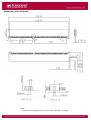
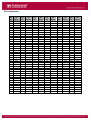
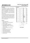
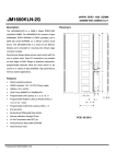
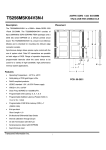
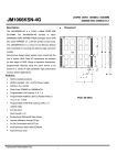
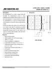
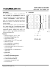
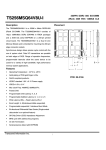
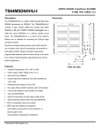
DDR3 VLP Unbuffered DIMM
DDR3 VLP Unbuffered DIMM is high-speed, low power memory module
that use DDR3 SDRAM in FBGA package and a 2048 bits serial
EEPROM on a 240-pin printed circuit board. DDR3 VLP Unbuffered
DIMM is a Dual In-Line Memory Module and is intended for mounting into
240-pin edge connector sockets.
Synchronous design allows precise cycle control with the use of system
clock. Data I/O transactions are possible on both edges of DQS. Range
of operation frequencies, programmable latencies allow the same device
to be useful for a variety of high bandwidth, high performance memory
system applications.
Features
•
RoHS compliant products.
•
JEDEC standard 1.5V ± 0.075V Power supply
•
VDDQ=1.5V ± 0.075V
•
Pin Identification
Symbol
Function
A0~A15, BA0~BA2
Address/Bank input
DQ0~DQ63
Bi-direction data bus.
Clock Freq: 667MHZ for 1333Mb/s/Pin.
DQS0~DQS7
Data strobes
•
Programmable CAS Latency: 6, 7, 8, 9
/DQS0~/DQS7
Differential Data strobes
Programmable Additive Latency (Posted /CAS):
CK0, /CK0,CK1, /CK1
Clock Input. (Differential pair)
•
CKE0, CKE1
Clock Enable Input.
ODT0, ODT1
On-die termination control line
/S0, /S1
DIMM rank select lines.
0,CL-2 or CL-1 clock
•
Programmable /CAS Write Latency (CWL)
=7 (DDR3-1333)
/RAS
Row address strobe
•
8 bit pre-fetch
/CAS
Column address strobe
•
Burst Length: 4, 8
/WE
Write Enable
•
Internal calibration through ZQ pin
DM0~DM7
Data masks/high data strobes
•
On Die Termination with ODT pin
VDD
Core power supply
VDDQ
I/O driver power supply
•
Serial presence detect with EEPROM
VREFDQ
•
Asynchronous reset
VDDSPD
I/O reference supply
Command/address reference
supply
SPD EEPROM power supply
SA0~SA2
Address select for EEPROM
SCL
Clock for EEPROM
SDA
Data for EEPROM
VSS
Ground
/RESET
Set DRAMs Known State
VTT
SDRAM I/O termination supply
NC
No Connection
VREFCA
Dimensions (Unit: millimeter)
Note:
1. Tolerances on all dimensions +/-0.15mm unless otherwise specified.
Pin Assignments
Pin
Pin
Pin
Pin
Pin
Pin
No
Name
No
Name
No
01
02
03
04
05
06
07
08
09
10
11
12
13
14
15
16
17
18
19
20
21
22
23
24
25
26
27
28
29
30
31
32
33
34
35
36
37
38
39
40
VREFDQ
VSS
DQ0
DQ1
VSS
/DQS0
DQS0
VSS
DQ2
DQ3
VSS
DQ8
DQ9
VSS
/DQS1
DQS1
VSS
DQ10
DQ11
VSS
DQ16
DQ17
VSS
/DQS2
DQS2
VSS
DQ18
DQ19
VSS
DQ24
DQ25
VSS
/DQS3
DQS3
VSS
DQ26
DQ27
VSS
NC
NC
41
42
43
44
45
46
47
48
49
50
51
52
53
54
55
56
57
58
59
60
61
62
63
64
65
66
67
68
69
70
71
72
73
74
75
76
77
78
79
80
VSS
NC
NC
VSS
NC
NC
VSS
NC
NC
CKE0
VDD
BA2
NC
VDD
A11
A7
VDD
A5
A4
VDD
A2
VDD
CK1,NC
/CK1,NC
VDD
VDD
VREFCA
NC
VDD
A10/AP
BA0
VDD
/WE
/CAS
VDD
/S1,NC
81
82
83
84
85
86
87
88
89
90
91
92
93
94
95
96
97
98
99
100
101
102
103
104
105
106
107
108
109
110
111
112
113
114
115
116
117
118
119
120
ODT1,NC
VDD
NC
VSS
Pin
Pin
Pin
Pin
Name
No
DQ32
DQ33
VSS
/DQS4
DQS4
VSS
DQ34
DQ35
VSS
DQ40
DQ41
VSS
/DQS5
DQS5
VSS
DQ42
DQ43
VSS
DQ48
DQ49
VSS
/DQS6
DQS6
VSS
DQ50
DQ51
VSS
DQ56
DQ57
VSS
/DQS7
DQS7
VSS
DQ58
DQ59
VSS
SA0
SCL
SA2
VTT
121
122
123
124
125
126
127
128
129
130
131
132
133
134
135
136
137
138
139
140
141
142
143
144
145
146
147
148
149
150
151
152
153
154
155
156
157
158
159
160
Pin
Pin
Name
No
VSS
DQ4
DQ5
VSS
DM0
NC
VSS
DQ6
DQ7
VSS
DQ12
DQ13
VSS
DM1
NC
VSS
DQ14
DQ15
VSS
DQ20
DQ21
VSS
DM2
NC
VSS
DQ22
DQ23
VSS
DQ28
DQ29
VSS
DM3
NC
VSS
DQ30
DQ31
VSS
NC
NC
VSS
161
162
163
164
165
166
167
168
169
170
171
172
173
174
175
176
177
178
179
180
181
182
183
184
185
186
187
188
189
190
191
192
193
194
195
196
197
198
199
200
Name
No
Name
NC
NC
VSS
NC
NC
VSS
NC
/RESET
201
202
203
204
205
206
207
208
209
210
211
212
213
214
215
216
217
218
219
220
221
222
223
224
225
226
227
228
229
230
231
232
233
234
235
236
237
238
239
240
DQ37
VSS
DM4
NC
VSS
DQ38
DQ39
VSS
DQ44
DQ45
VSS
DM5
NC
VSS
DQ46
DQ47
VSS
DQ52
DQ53
VSS
DM6
NC
VSS
DQ54
DQ55
VSS
DQ60
DQ61
VSS
DM7
NC
VSS
DQ62
DQ63
VSS
VDDSPD
SA1
SDA
VSS
VTT
CKE1,NC
VDD
A15
A14
VDD
A12
A9
VDD
A8
A6
VDD
A3
A1
VDD
VDD
CK0
/CK0
VDD
NC
A0
VDD
BA1
VDD
/RAS
/S0
VDD
ODT0
A13
VDD
NC
VSS
DQ36