1
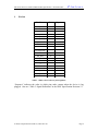
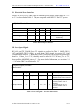
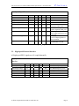
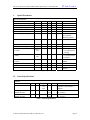
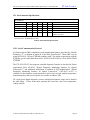
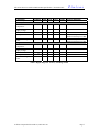
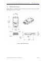
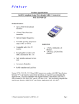
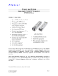
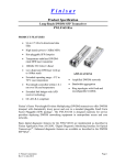
Finisar
Product Specification
RoHS Compliant 2.125 Gb/s Short-Wavelength GBIC Transceiver
FTL-8519-3D-2.5
Product Features
•
Up to 2.125 Gb/s bi-directional
data links
•
850nm VCSEL Laser
Transmitter
•
Optional Digital Diagnostics
Functions
•
Extended Operating Temperature
Range (-10°C to +85°C)
•
Compatible with 3.3V & 5V
Systems
•
Hot-Pluggable (complies with
GBIC specification Rev. 5.5)
•
Fully metallic enclosure for low
EMI
•
Low power dissipation
•
RoHS compliant and Lead Free
Applications
•
1.25 Gb/s 1000BASE-LX
Ethernet
•
Dual Rate 1.06 / 2.125 Gb/s
Fibre Channel
Finisar’s FTL-8519-3D-2.5 850nm GBIC transceivers comply with GBIC Specification
Revision 5.51. They are compatible with the Gigabit Ethernet as specified in IEEE Std
802.32, Fibre Channel FC-PH, PH2, PH33 and FC-PI-2 Rev. 10.04. They are RoHS
compliant and lead-free per Directive 2002/95/EC5 and Finisar Application Note AN20389.
© Finisar Corporation November 16, 2007 Rev. D3
Page 1
FTL-8519-3D-2.5 2.125Gb/s GBIC Product Specification – November 2007
I.
F i n i s a r
Pin Out
Pin Name
Pin #
Sequence
RX_LOS
1
2
GND
2
2
GND
3
2
MOD_DEF(0)
4
2
MOD_DEF(1)
5
2
MOD_DEF(2)
6
2
TX_DISABLE
7
2
GND
8
2
GND
9
2
TX_FAULT
(not supported)
GND
10
2
11
1
-RX_DAT
12
1
+RX_DAT
13
1
GND
14
1
VCC
15
2
VCC
16
2
GND
17
1
+TX_DAT
18
1
-TX_DAT
19
1
GND
20
1
Table 1. GBIC to host connector pin assignment
“Sequence” indicates the order in which pins make contact when the device is hot
plugged. Also see “Table 3: Signal Definitions” in the GBIC Specification Revision 5.5.1
© Finisar Corporation November 16, 2007 Rev. D3
Page 2
FTL-8519-3D-2.5 2.125Gb/s GBIC Product Specification – November 2007
II.
F i n i s a r
Electrical Power Interface
Finisar FTL-8519-3D-2.5 GBICs have an extended power supply voltage range of 3.15 V
to 5.5 V as described in Table 2. They are compatible with both 3.3V and 5 V systems.
+5/3.3 Volt Electrical Power
Interface
Parameter
Supply Current
Surge Current
Symbol
Is
Isurge
Min
Absolute Supply Voltage
Vmax
-0.3
Operating Supply Voltage
Vcc
3.15
Typ
190
3.3, 5
Max
300
330
Units
mA
mA
Notes/Conditions
6
V
Not to be applied
continuously
5.5
V
Referenced to GND.
Hot plug
Table 2. Electrical power interface
III. Low Speed Signals
RX_LOS, and TX_DISABLE are TTL signals as described in Table 3. MOD_DEF(1)
(SCL) and MOD_DEF(2) (SDA), are open drain CMOS signals (see section VI, “Serial
Communication Protocol”). Both MOD_DEF(1) and MOD_DEF(2) must be pulled up to
host_Vcc. If host_Vcc is 3.3V, then they must be pulled to 3.3V. If host_Vcc is 3.3V,
do not pull the MOD_DEF pins to 5V. For more detailed information, see sections 5.3.1
– 5.3.8 in the GBIC Specification Rev. 5.51.
Low Speed Signals, Electronic
Characteristics
Parameter
GBIC Output LOW
Symbol
VOL
GBIC Output HIGH
VOH
GBIC Input LOW
VIL
GBIC Input HIGH
VIH
Min
0
Max
0.5
Units Notes/Conditions
V
4.7k to 10k pull-up to host_Vcc,
measured at host side of connector
host_Vcc - 0.5 host_Vcc + 0.3
V
4.7k to 10k pull-up to host_Vcc,
measured at host side of connector
0
0.8
V
4.7k to 10k pull-up to Vcc,
measured at GBIC side of
connector*
2
Vcc + 0.3
V
4.7k to 10k pull-up to Vcc,
measured at GBIC side of
connector*
*Note VIH and VIL are the same for both 5V and 3.3V operation
Table 3. Low speed signals – electronic characteristics
© Finisar Corporation November 16, 2007 Rev. D3
Page 3
FTL-8519-3D-2.5 2.125Gb/s GBIC Product Specification – November 2007
F i n i s a r
Low Speed Signal Parameters
Parameter
Symbol
RX_LOS Assert Level
RX_LOS Deassert Level
RX_LOS Hysteresis
RX_LOS Assert Delay
Min
Typ
--30
--0.5
t_loss_on
RX_LOS Negate Delay
TX_DISABLE Assert Time
TX_DISABLE Negate Time
TX_DISABLE Reset Time
Max
Units Notes/Conditions
dBm
dBm
dB
44
100
μsec From detection of loss of signal
to assertion of RX_LOS
t_loss_off
44
100
μsec From detection of presence of
signal to negation of RX_LOS
t_off
10
μsec Rising edge of TX_DISABLE to
fall of output signal below 10%
of nominal
t_on
1000 μsec Falling edge of TX_DISABLE
to rise of output signal above
90% of nominal
t_reset
10
μsec TX_DISABLE HIGH before
TX_DISABLE set LOW
Table 4. Low speed signal parameters
-19
IV. High Speed Electrical Interface
All high-speed PECL signals are AC-coupled internally.
High Speed Electrical
Interface
Parameter
Data Input Voltage
Data Output Voltage
PECL rise/fall
Bit Error Rate
Tx Input Impedance
Rx Output Impedance
Symbol
Vin
Vout
tr,tf
BER
Zin
Zout
Min
650
370
Typ
75
75
Max
2000
2000
175
10-12
Units
mV
mV
psec
Notes/Conditions
PECL differential peak - peak
PECL differential peak - peak
20%-80% differential
PRBS 27 - 1 test data pattern
ohm
ohm
Table 5. High-speed electrical interface
© Finisar Corporation November 16, 2007 Rev. D3
Page 4
F i n i s a r
FTL-8519-3D-2.5 2.125Gb/s GBIC Product Specification – November 2007
V.
Optical Parameters
Optical Parameters
Parameter
Transmitter Center Wavelength
Transmitter Spectral Width (RMS)
Transmitter Optical Output Power
Transmitter Extinction Ratio
Relative Intensity Noise
Transmitter Eye Opening
Total Transmitter Jitter
Symbol
λc
Δλ
Pout
ER
RIN
--
Min
820
Typ
850
0.5
-9.5
9
-117
60
TJTX
Transmitter Rise/Fall Time
Optical Input Wavelength
Optical Receiver Sensitivity
<=1.25Gb/s
Tr/Tf
λin
RXSENS
(1X)
Optical Receiver Sensitivity
>1.25Gb/s
RXSENS
(2X)
Stressed Receiver Sensitivity
@1.25Gb/s
Average Received Power
Max Reflectivity
Total Receiver Jitter
Max
860
0.85
-3.5
160
770
-22
160
860
-20.5
-15
-13.5
0
-14
160
RXMAX
TJRX
Units
nm
nm
dBm
dB
dB/Hz
%
ps
Notes/Conditions
RMS
Average Power
Conforms to IEEE
802.3 and Fibre
Channel Eye Masks
Peak to peak, filtered
ps
Unfiltered 20%-80%
nm
dBm BER < 10-12 w/ PRBS
27 - 1 test data pattern
@ 1.25Gb/s
dBm BER < 10-12 w/ PRBS
27 - 1 test data pattern
@ 2.125Gb/s
DBm As defined in GBE
standard
dBm
dB
ps
Peak to peak, filtered in
loopback
Table 6. Optical parameters
VI. General Specifications
General
Parameter
Data Rate
Fiber Length on 50μm
500MHz-km Fiber
Fiber Length 62.5μm
200MHz-km Fiber
Symbol Min
BR
L
L
Typ
1.0625,
1.25,
2.125
Units Notes/Conditions
Gb/sec 1x/2x Fibre Channel, IEEE 802.3
Compatible. Rate tolerance =
±100ppm
550
m
@1.0625Gb/s
(300)
(@2.125Gb/s)
275
m
@1.0625Gb/s
(150)
(@2.125Gb/s)
Table 7. General specifications
© Finisar Corporation November 16, 2007 Rev. D3
Max
Page 5
FTL-8519-3D-2.5 2.125Gb/s GBIC Product Specification – November 2007
F i n i s a r
VII. Environmental Specifications
Environment
Parameter
Operating Temp
Relative Humidity
Storage Temp
Eye Safety
Symbol
Min
Top
RH
Tsto
--
-10
0
-40
Typ
Max
85
85
85
Units Notes/Conditions
°C
%
°C
Case Temperature
Non Condensing
CDRH and IEC-825 Class 1 Laser
Product. See Note 1
Note 1: Complies with FDA performance standards for laser products except for deviations pursuant to
Laser Notice No. 50, dated July 26, 2001.
Table 8. Environmental Specifications
VIII. Serial Communication Protocol
All Finisar optical GBICs implement serial identification features described for ‘Module
Definition “4”’ as outlined in Annex D of the GBIC Specification1. These GBICs use an
Atmel AT24C01A 128 byte E2PROM at address A0H. For details on interfacing with the
E2PROM, see the Atmel data sheet titled “AT24C01A/02/04/08/16 2-Wire Serial CMOS
E2PROM.”6
The FTL-8519-3D-2.5 also supports extended diagnostic features as described in Finisar
Applications Note AN-2030, “Digital Diagnostic Monitoring Interface for Optical
Transceivers”8, and additional information is available in SFF standard titled: “Digital
Diagnostic Monitoring Interface for Optical Transceivers”7 (SFF-8472 rev9.3). A
controller IC that monitors system parameters such as laser current, module temperature,
transmitter power, and received power is accessible at address A2H.
I2C clock speed, digital diagnostic accuracy and digital diagnostic range can be found in
the table below. Values in the table represent the worst-case values over temperature,
voltage, and life.
© Finisar Corporation November 16, 2007 Rev. D3
Page 6
F i n i s a r
FTL-8519-3D-2.5 2.125Gb/s GBIC Product Specification – November 2007
Parameter
I2C Clock Speed
Accuracy
Internal Transceiver
Temperature
Internal Transceiver
Supply Voltage
Tx Bias Current
Tx Output Power
Received Average
Power
Range
Internal Transceiver
Temperature
Internal Transceiver
Supply Voltage
Tx Bias Current
Tx Output Power
Received Average
Power
Symbol
Min Typ
Max
Units Notes/Conditions
0
100,000
Hz
Bus can be driven blind
DDTemperature
-3
+3
°C
Measured at controller IC
DDVoltage
-3
+3
%
Measured at controller IC
DDBias
DDTxPower
-10
-3
+10
+3
%
dB
DDRxPower
-3
+3
dB
DDTemperature
-40
100
°C
DDVoltage
3.0
6.0
V
DDBias
DDTxPower
DDRxPower
0
-12
-20
15
-2
1
mA
dBm
dBm
100% tested in production
tested at room temp to ±2 dB
100% tested in production
tested at room temp to ±2 dB
Table 9. Digital Diagnostic Accuracy and Range Limits
© Finisar Corporation November 16, 2007 Rev. D3
Page 7
FTL-8519-3D-2.5 2.125Gb/s GBIC Product Specification – November 2007
X.
F i n i s a r
Mechanical Specifications
Finisar GBICs are compatible with the mechanical specifications outlined in the GBIC
Specification Revision 5.5, Section 61.
Figure 1. GBIC Outline Drawing
© Finisar Corporation November 16, 2007 Rev. D3
Page 8
FTL-8519-3D-2.5 2.125Gb/s GBIC Product Specification – November 2007
F i n i s a r
XI. References
1.
“Gigabit Interface Converter (GBIC) Revision 5.5”. Sun Microsystems Computer
Company et. al., September 27, 2000. http://playground.sun.com/pub/OEmod/
2.
IEEE Std 802.3. IEEE Standards Department, 2002.
3.
“Fibre Channel Physical and Signaling Interface (FC-PH, FC-PH2, FC-PH3)”.
American National Standard for Information Systems.
4.
Fibre Channel Draft Physical Interface Specification (FC-PI-2 Rev. 10.0).
American National Standard for Information Systems.
5.
Directive 2002/95/EC of the European Council Parliament and of the Council, “on
the restriction of the use of certain hazardous substances in electrical and electronic
equipment.” January 27, 2003.
6.
“AT24C01A/02/04/08/16 2-Wire Serial CMOS E2PROM”. Atmel Corporation.
www.Atmel.com
7.
“Digital Diagnostics Monitoring Interface for Optical Transceivers”. SFF
Document Number SFF-8472, Revision 9.3.
8.
“Application Note AN-2030: Digital Diagnostic Monitoring Interface for Optical
Transceivers”, Finisar Corporation, April 2002.
9.
“Application Note AN-2038: Finisar Implementation of RoHS Compliant
Transceivers”, Finisar Corporation, March 2005.
XI.
For More Information
Finisar Corporation
1389 Moffett Park Drive
Sunnyvale, CA 94089-1134
Tel. 1-408-548-1000
Fax 1-408-541-6138
[email protected]
www.finisar.com
© Finisar Corporation November 16, 2007 Rev. D3
Page 9