1
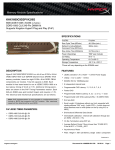
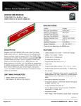
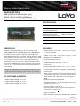
Memory Module Specifications
KHX16LS9P1K2/8
8GB (4GB 1Rx8 512M x 64-Bit x 2 pcs.)
DDR3L-1600 CL9 204-Pin SODIMM Kit
Supports Kingston HyperX Plug and Play (PnP)
SPECIFICATIONS
CL(IDD)
9 cycles
Row Cycle Time (tRCmin)
48.125ns (min.)
Refresh to Active/Refresh
Command Time (tRFCmin)
260ns (min.)
Row Active Time (tRASmin)
33.75ns (min.)
Maximum Operating Power
(DDR3-1600 CL9-9-9 @ 1.35V)
TBD W* (per module)
UL Rating
94 V - 0
Operating Temperature
0o C to 85o C
Storage Temperature
-55o C to +100o C
*Power will vary depending on the SDRAM used.
DESCRIPTION
FEATURES
Kingston's KHX16LS9P1K2/8 is a kit of two 512M x 64-bit
(4GB) DDR3L-1600 CL9 SDRAM (Synchronous DRAM) 1Rx8
•
JEDEC standard 1.35V (1.28V ~ 1.45V) and 1.5V (1.425V ~
1.575V) Power Supply
•
•
•
•
•
•
•
•
•
VDDQ = 1.35V (1.28V ~ 1.45V) and 1.5V (1.425V ~ 1.575V)
•
•
Bi-directional Differential Data Strobe
•
•
On Die Termination using ODT pin
•
•
Asynchronous Reset
low voltage memory modules, based on eight 512M x 8-bit
DDR3 FBGA components per module. Total kit capacity is 8GB.
Each module kit has been tested to run at JEDEC DDR3L-1600
at a low latency timing of 9-9-9 at 1.35V. Additional timing
parameters are shown in the PnP Timing Parameters section.
Each 204-pin SODIMM uses gold contact fingers and requires
1.35V or +1.5V. The electrical and mechanical specifications
are as follows:
Note: PnP implementation is only possible in configurations that
include a BIOS that supports the PnP function. Your maximum
speed will be determined by your BIOS.
PnP JEDEC TIMING PARAMETERS:
•
•
•
DDR3-1600 CL9-9-9 @1.35V or 1.5V
DDR3-1333 CL8-8-8 @1.35V or 1.5V
DDR3-1066 CL6-6-6 @1.35V or 1.5V
800MHz fCK for 1600Mb/sec/pin
8 independent internal bank
Programmable CAS Latency: 11, 10, 9, 8, 7, 6
Posted CAS
Programmable Additive Latency: 0, CL - 2, or CL - 1 clock
Programmable CAS Write Latency(CWL) = 8 (DDR3-1600)
8-bit pre-fetch
Burst Length: 8 (Interleave without any limit, sequential with
starting address “000” only), 4 with tCCD = 4 which does not
allow seamless read or write [either on the fly using A12 or
MRS]
Internal(self) calibration : Internal self calibration through ZQ
pin (RZQ : 240 ohm ± 1%)
Average Refresh Period 7.8us at lower than TCASE 85°C,
3.9us at 85°C < TCASE < 95°C
PCB : Height 1.180” (30.00mm), double sided component
Continued >>
Document No. 4806574-001.D00
05/15/13
Page 1
continued
HyperX
MODULE DIMENSIONS
(units = millimeters)
FOR MORE INFORMATION, GO TO WWW.KINGSTON.COM
All Kingston products are tested to meet our published specifications. Some motherboards or system configurations may not operate at
the published HyperX memory speeds and timing settings. Kingston does not recommend that any user attempt to run their computers
faster than the published speed. Overclocking or modifying your system timing may result in damage to computer components.
Document No. 4806574-001.D00
Page 2