1
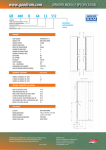
Technical Datasheet
BD256TEC400
(256MB / PC3200)
BD512TEC500
(512MB / PC3200)
Rev. 1.1 / Breisach, 07/2005
DESCRIPTION
The takeMS 184pin DDR SDRAM DIMM series is unbuffered 184-pin double data rate Synchronous DRAM Dual
In-Line Memory Modules which are organized as 32/64Mx64 high-speed memory arrays. The modules (Single Side
or Double Side) consists of eight or sixteen 32Mx8 DDR SDRAM in 400mil TSOP II packages on a 184pin glassepoxy substrate. It is suitable for easy interchange and addition.
The takeMS 184pin DDR SDRAM DIMM series is designed for high speed of up to 200MHz and offers fully
synchronous operations referenced to both rising and falling edges of differential clock inputs. While all addresses
and control inputs are latched on the rising edges of the clock, Data(DQ), Data strobes(DQS) and Write data masks
inputs are sampled on both rising and falling edges of it. The data paths are internally pipelined and 2-bit
prefetched to achieve very high bandwidth. All input and output voltage levels are compatible with SSTL_2. High
speed frequencies, programmable latencies and burst lengths allow variety of device operation in high performance
memory system.
The takeMS 184pin DDR SDRAM DIMM series incorporates SPD (serial presence detect).
Serial presence detect function is implemented via a serial 2,048-bit EEPROM. The first 128 bytes of serial PD data
are programmed by takeMS to identify DIMM type, capacity and other information of DIMM.
FEATURES
* 256/512MB Unbuffered DDR DIMM based on
* Data(DQ), Data strobes & Write masks latched
32Mx8 DDR SDRAM
on both rising & falling edges of the clock
* JEDEC Standard 184pin dual in-line memory module(DIMM)
* 2.6V +/- 0.2V VDD & VDDQ Power supply
* Data inputs on DQS centers when write (centered DQ)
* Programmable CAS Latency 2 /2.5 supported
* Data strobes synchronized with output data for read & input
* Internal four bank operations with single pulsed
data for write
RAS
* All inputs & outputs are compatible with SSTL_2 interface
* Auto refresh& self refresh supported
* Fully differential clock operations (CLK & CLK) with
* Programmable Burst Length 2/4/8 with both
200MHz
sequential 7 interleave mode
* All addresses & control inputs except Data, Data strobes &
* 4096 refresh cycles / 64ms
Data masks latched on the rising edges of the clock
Clock
Frequency
200MHz (PC3200)
DDR 400 CL2.5=200
DDR 333 CL2.5=166
DDR 266 CL2=133
Interface
Power
Supply
SDRAM
Package
SSTL_2
VDD=2.6V
VDDQ=2.6V
400mil 66pin
TSOP II
Jul 2005
This document is a general product description and is subject to change without notice. takeMS does not assume any responsibility for use of
circuits described. No patent licenses are implied. takems is a trademark of Memorysolution GmbH
32/64Mx64 bits
M
184PIN PC3200 DDR SDRAM DIM
DIMM
184 PIN 64 BIT DDR SDRAM DIMM
PIN DESCRIPTION
Pin
CK0,/CK0,CK1,/CK1,CK2,/CK2
CS0
CKE0
/RAS, /CAAS, /WE
A0 – A11
BA0, BA1
DQ0 – DQ63
DQS0 – DQS7
DM0 – DM7
VDD
Pin Description
Differential Clock Inputs
Chip Select Input
Clock Enable Input
Command Sets Inputs
Address
Bank Address
Data Inputs/Outputs
Data Strobe Inputs/Outputs
Data-in Mask
Power Supply
Pin
VDDQ
VSS
VREF
VDDSPD
SA0 – SA2
SCL
SDA
VDDID
DU
NC
Pin Description
DQs Power Supply
Ground
Reference Power Supply
Power Supply for SPD
EEPROM Address Inputs
EEPROM Clock
EEPROM Data I/O
VDD Identification Flag
Do not Use
No Connection
PIN ASSIGNMENT
PIN
1
2
3
4
5
6
7
8
9
10
11
12
13
14
15
16
17
18
19
20
21
22
23
24
25
26
27
28
29
30
31
NAME
VREF
DQ0
VSS
DQ1
DQS0
DQ2
VDD
DQ3
NC
NC
VSS
DQ8
DQ9
DQS1
VDDQ
CKO
/CK0
VSS
DQ10
DQ11
CKE0
VDDQ
DQ16
DQ17
DQS2
VSS
A9
DQA8
A7
VDDQ
DQ19
PIN
32
33
34
35
36
37
38
39
40
41
42
43
44
45
46
47
48
49
50
51
52
53
54
55
56
57
58
59
60
61
NAME
A5
DQ24
VSS
DQ25
DQS3
A4
VDD
DQ26
DQ27
A2
Vss
A1
CB0*
CB1*
VDD
DQS8*
A0
CB2*
VSS
CB3*
BA1
KEY
DQ32
VDDQ
DQ33
DQS4
DQ34
VSS
BA0
DQ35
DQ40
PIN
62
63
64
65
66
67
68
69
70
71
72
73
74
75
76
77
78
79
80
81
82
83
84
85
86
87
88
89
90
91
92
NAME
VDDQ
/WE
DQ41
/CAS
VSS
DQS5
DQ42
DQ43
VDD
NC
DQ48
DQ49
VSS
/CK2
CK2
VDDQ
DQS6
DQ50
DQ51
VSS
VDDID
DQ56
DQ57
VDD
DQS7
DQ58
DQ59
VSS
WP
SDA
SCL
PIN
93
94
95
96
97
98
99
100
101
102
103
104
105
106
107
108
109
110
111
112
113
114
115
116
117
118
119
120
121
122
123
NAME
VSS
DQ4
DQ5
VDDQ
DM0
DQ6
DQ7
VSS
NC
NC
A13*
VDDQ
DQ12
DQ13
DM1
VDD
DQ14
DQ15
CKE1
VDDQ
BA2*
DQ20
A12*
VSS
DQ21
A11
DM2
VDD
DQ22
A8
DQ23
PIN
124
125
126
127
128
129
130
131
132
133
134
135
136
137
138
139
140
141
142
143
144
NAME
VSS
A6
DQ28
DQ29
VDDQ
DM3
A3
DQ30
VSS
DQ31
CB4*
CB5*
VDDQ
CK1
/CK1
VSS
DM8*
A10
CB6*
VDDQ
CB7*
KEY
145
VSS
146
DQ36
147
DQ37
148
VDD
149
DM4
150
DQ38
151
DQ39
152
VSS
153
DQ44
PIN
154
155
156
157
158
159
160
161
162
163
164
165
166
167
168
169
170
171
172
173
174
175
176
177
178
179
180
181
182
183
184
NAME
/RAS
DQ45
VDDQ
/CS0
/CS1
DM5
VSS
DQ46
DQ47
NC
VDDQ
DQ52
DQ53
NC
VDD
DM6
DQ54
DQ55
VDDQ
NC
DQ60
DQ61
VSS
DM7
DQ62
DQ63
VDDQ
SA0
SA1
SA2
VDDSPD
32/64Mx64 bits
184PIN PC3200 DDR SDRAM DIMM
BLOCK DIAGRAM
184 PIN x64 DDR SDRAM DIMM, 1 Bank with x8 DDR SDRAMs
32/64Mx64 bits
184PIN PC3200 DDR SDRAM DIMM
BLOCK DIAGRAM
184 PIN x64 DDR SDRAM DIMM, 2 Bank with x8 DDR SDRAMs
32/64Mx64 bits
0 DDR SDRAM DIM
M
184PIN PC320
PC3200
DIMM
32/64Mx64 bits
0 DDR SDRAM DIMM
184PIN PC320
PC3200
32/64Mx64 bits
184PIN PC3200 DDR SDRAM DIMM
32/64Mx64 bits
184PIN PC3200 DDR SDRAM DIMM
32/64Mx64 bits
184PIN PC3200 DDR SDRAM DIMM
Serial Presence Detect
256M Bytes for Unbuffered & Non ECC Module (DDR400 use 32Mx8 *8pcs)
Byte Description
Function
Hex Value
No.
0
1
2
3
4
5
6
7
8
9
10
11
12
13
14
15
16
17
18
19
20
21
Number of Serial PD Bytes used
Total number of Bytes in Serial PD device
Fundamental Memory Type
# of Row Addresses on this assembly
# of Column Addresses on this assembly
# of Physical Banks on DIMM
Data Width of this assembly
Data Width of this assembly(Continued)
Voltage Interface Level of this assembly
DDRAM Cycle time at CAS Latency=2.5
DDRAM Access from Clock at CAS Latency=2.5
DIMM configuration type(Non-parity, Parity or ECC)
Refresh Rate/Type
Primary SDRAM Width
Error Checking SDRAM Width
Min. Clock Delay, Back-to-Back Random Column Access
Burst Lengths Supported
Number of Banks on SDRAM Device
CAS Latency
Chip Select Latency
Write Latency
DDR SDRAM Module Attributes
22
DDRAM Device Attributes: General
23
24
25
26
27
28
29
30
31
32
33
34
35
36-40
41
42
43
44
45
46-61
62
63
64-71
72
DDRAM Cycle time at CAS Latency=2
DDRAM Access from Clock at CAS Latency=2
DDRAM Cycle time at CAS Latency=1.5
DDRAM Access from Clock at CAS Latency=1.5
Minimum Row Precharge Time (tRP)
Minimum Row Active to Row Active delay (tRRD)
Minimum RAS to CAS delay (tRCD)
Minimum Active to Precharge Time (tRAS)
Module Bank Density
Address and Command Input Setup Time Before Clock
Address and Command Input Hold Time After Clock
Data/Data Mask Input Setup Time Before Data Strobe
Data/Data Mask Input Hold Time After Data Strobe
Reserved
Minimum active /auto-refresh time(tRC)
Minimum auto-refresh to active command period (tRFC)
Maximum cycle time(Tck max)
Maximum DQS-DQ skew time(tDQSQ)
Maximum read data hold skew factor(tQHS)
Reserved
SPD Revision
Checksum for Bytes 0-62
Manufacturer’s JEDEC ID Code
Module Manufacturing Location
73-90 Module Part Number
91-92
93-94
95-98
99-127
128-255
Module Revision Code
Module Manufacturing Date
Module Serial Number
Manufacturer’s Specific Data
Open for customer use
128 bytes
256 bytes
DDR SDRAM
13
10
1 ROWS
64 bit
0
SSTL_2.5V
5 ns
+/- 0.7 ns
Non-parity
7.8 us
X8 bit
None
Tccd=1 clk
2,4,8
4 Banks
2.5
0 clk
1 clk
Unbuffer
+/- 0.2v voltage
tolerance
7.5ns
+/- 0.7 ns
None
None
15 ns
10 ns
15 ns
40 ns
256M of 1 row
0.6 ns
0.6 ns
0.4 ns
0.4 ns
Reserved
55 ns
70 ns
10 ns
0.4 ns
0.50 ns
Reserved
Rev0.0
BD256TEC400
Reserved
YY-WW
Reserved
Reserved
Reserved
80h
08h
07h
0Dh
0Ah
01h
40h
00h
04h
50h
70h
00h
82h
08h
00h
01h
0eh
04h
08h
01h
02h
20h
00h
75h
70h
00h
00h
3Ch
28h
3Ch
28h
40h
60h
60h
40h
40h
00h
37h
46h
28h
28h
50h
00h
00h
BDh
7F, 7F, 7F, 58h
31h
42, 44, 32, 35, 36,
54, 45, 43, 34, 30,
30h
00h
00h
00h
00h
32/64Mx64 bits
184PIN PC3200 DDR SDRAM DIMM
Serial Presence Detect
512M Bytes for Unbuffered & Non ECC Module (DDR400 use 32Mx8 *16pcs)
Byte Description
Function
Hex Value
No.
0
1
2
3
4
5
6
7
8
9
10
11
12
13
14
15
16
17
18
19
20
21
Number of Serial PD Bytes used
Total number of Bytes in Serial PD device
Fundamental Memory Type
# of Row Addresses on this assembly
# of Column Addresses on this assembly
# of Physical Banks on DIMM
Data Width of this assembly
Data Width of this assembly(Continued)
Voltage Interface Level of this assembly
DDRAM Cycle time at CAS Latency=2.5
DDRAM Access from Clock at CAS Latency=2.5
DIMM configuration type(Non-parity, Parity or ECC)
Refresh Rate/Type
Primary SDRAM Width
Error Checking SDRAM Width
Min. Clock Delay, Back-to-Back Random Column Access
Burst Lengths Supported
Number of Banks on SDRAM Device
CAS Latency
Chip Select Latency
Write Latency
DDR SDRAM Module Attributes
22
DDRAM Device Attributes: General
23
24
25
26
27
28
29
30
31
32
33
34
35
36-40
41
42
43
44
45
46-61
62
63
64-71
72
DDRAM Cycle time at CAS Latency=2
DDRAM Access from Clock at CAS Latency=2
DDRAM Cycle time at CAS Latency=1.5
DDRAM Access from Clock at CAS Latency=1.5
Minimum Row Precharge Time (tRP)
Minimum Row Active to Row Active delay (tRRD)
Minimum RAS to CAS delay (tRCD)
Minimum Active to Precharge Time (tRAS)
Module Bank Density
Address and Command Input Setup Time Before Clock
Address and Command Input Hold Time After Clock
Data/Data Mask Input Setup Time Before Data Strobe
Data/Data Mask Input Hold Time After Data Strobe
Reserved
Minimum active /auto-refresh time(tRC)
Minimum auto-refresh to active command period (tRFC)
Maximum cycle time(Tck max)
Maximum DQS-DQ skew time(tDQSQ)
Maximum read data hold skew factor(tQHS)
Reserved
SPD Revision
Checksum for Bytes 0-62
Manufacturer’s JEDEC ID Code
Module Manufacturing Location
73-90 Module Part Number
91-92
93-94
95-98
99-127
128-255
Module Revision Code
Module Manufacturing Date
Module Serial Number
Manufacturer’s Specific Data
Open for customer use
128 bytes
256 bytes
DDR SDRAM
13
10
2 ROWS
64 bit
0
SSTL_2.5V
5 ns
+/- 0.7 ns
Non-parity
7.8 us
X8 bit
None
Tccd=1 clk
2,4,8
4 Banks
2.5
0 clk
1 clk
Unbuffer
+/- 0.2v voltage
tolerance
7.5ns
+/- 0.7 ns
None
None
15 ns
10 ns
15 ns
40 ns
256M of 1 row
0.6 ns
0.6 ns
0.4 ns
0.4 ns
Reserved
55 ns
70 ns
10 ns
0.4 ns
0.50 ns
Reserved
Rev0.0
BD512TEC500
Reserved
YY-WW
Reserved
Reserved
Reserved
80h
08h
07h
0Dh
0Ah
02h
40h
00h
04h
50h
70h
00h
82h
08h
00h
01h
0eh
04h
08h
01h
02h
20h
00h
75h
70h
00h
00h
3Ch
28h
3Ch
28h
40h
60h
60h
40h
40h
00h
37h
46h
28h
28h
50h
00h
00h
BEh
7F, 7F, 7F, 58h
31h
42, 44, 35, 31, 32,
54, 45, 43, 35, 30,
30h
00h
00h
00h
00h
32/64Mx64 bits
184PIN PC3200 DDR SDRAM DIMM
PACKAGE DIMENSIONS
133.44mm+/-0.15mm
2.86mm+/-.1mm
29.55mm+/-0.15mm
3.58mm+/-.1mm
1
52
92
53
73.2mm+/-.1mm
1.32mm+/-.1mm
60.2mm+/-.1mm
3.97mm+/-.1mm
18.0mm+/-.1mm
10mm+/-.1mm
R1.21mm+/-.1mm
184
145
3.8mm+/-.1mm
2.5mm+/-0.5mm
184
0.27mm+/-0.5mm
144
1.76mm+/-.1mm
93
2.3mm+/-.1mm