1
168 PIN PC100 Unbuffered DIMM
256MB With 16M X8 CL2
TS32MLS64V8D2
Description
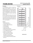
Placement
The TS32MLS64V8D2 is a 64M bit x 64 Synchronous
Dynamic
RAM
high-density
for
PC-100.
The
TS32MLS64V8D2 consists of 16pcs CMOS 16Mx8 bits
Synchronous DRAMs in TSOP-II 400mil packages and
a 2048 bits serial EEPROM on a 168-pin printed circuit
board. The TS32MLS64V8D2 is a Dual In-Line
Memory Module and is intended for mounting into
168-pin edge connector sockets.
Synchronous design allows precise cycle control with
the use of system clock. I/O transactions are possible
on every clock cycle. Range of operation frequencies,
A
programmable latencies allow the same device to be
useful
for
a
variety
of
high
bandwidth,
high
performance memory system applications.
Features
• Performance Range: PC-100 CL2.
B
• Burst Mode Operation.
D
• Auto and Self Refresh.
• CKE Power Down Mode.
E
• DQM Byte Masking (Read/Write)
C
• Serial Presence Detect (SPD) with serial EEPROM
• LVTTL compatible inputs and outputs.
• Single 3.3V ± 0.3V power supply.
I
E
H
• MRS cycle with address key programs.
G
Latency (Access from column address)
F
Burst Length (1,2,4,8 & Full Page)
Data Sequence (Sequential & Interleave)
• All inputs are sampled at the positive going edge of
PCB: 09-7308
the system clock.
Transcend information Inc
1
168 PIN PC100 Unbuffered DIMM
256MB With 16M X8 CL2
TS32MLS64V8D2
Dimensions
Side
Pin Identification
Millimeters
Symbol
Inches
Function
A
133.35±0.40
5.250±0.016
A0~A11,BA0,BA1 Address input
B
65.67
2.585
DQ0~DQ63
Data Input / Output.
C
23.49
0.925
D
8.89
0.350
CLK0~CLK3
Clock Input.
E
3.00
0.118
CKE0, CKE1
Clock Enable Input.
F
29.21±0.20
1.150±0.008
/CS0~/CS3
Chip Select Input.
G
19.80
0.780
/RAS
Row Address Strobe
H
15.80
0.622
I
1.27±0.10
0.050±0.004
/CAS
Column Address Strobe
/WE
Write Enable
DQM0~DQM7
Data (DQ) Mask
SA0~SA2
Address in EEPROM
SCL
Serial PD Clock
SDA
Serial PD Add/Data input/output
Vcc
+3.3 Voltage Power Supply
Vss
Ground
NC
No Connection
(Refer Placement)
Transcend information Inc
2
168 PIN PC100 Unbuffered DIMM
256MB With 16M X8 CL2
TS32MLS64V8D2
Pinouts:
Pin
Pin
Pin
Pin
No
Name
No
Name
01
Vss
43
Vss
02
DQ0
44
NC
03
DQ1
45
/CS2
04
DQ2
46
DQM2
05
DQ3
47
DQM3
06
Vcc
48
NC
07
DQ4
49
Vcc
08
DQ5
50
NC
09
DQ6
51
NC
10
DQ7
52
*CB2
11
DQ8
53
*CB3
12
Vss
54
Vss
13
DQ9
55
DQ16
14
DQ10
56
DQ17
15
DQ11
57
DQ18
16
DQ12
58
DQ19
17
DQ13
59
Vcc
18
Vcc
60
DQ20
19
DQ14
61
NC
20
DQ15
62
*Vref
21
*CB0
63
*CKE1
22
*CB1
64
Vss
23
Vss
65
DQ21
24
NC
66
DQ22
25
NC
67
DQ23
26
Vcc
68
Vss
27
/WE
69
DQ24
28
DQM0
70
DQ25
29
DQM1
71
DQ26
30
/CS0
72
DQ27
31
NC
73
Vcc
32
Vss
74
DQ28
33
A0
75
DQ29
34
A2
76
DQ30
35
A4
77
DQ31
36
A6
78
Vss
37
A8
79
*CLK2
38
A10/AP
80
NC
39
BA1
81
NC
40
Vcc
82
SDA
41
Vcc
83
SCL
42
CLK0
84
Vcc
* Please refer Block Diagram
Transcend information Inc
Pin
No
85
86
87
88
89
90
91
92
93
94
95
96
97
98
99
100
101
102
103
104
105
106
107
108
109
110
111
112
113
114
115
116
117
118
119
120
121
122
123
124
125
126
3
Pin
Name
Vss
DQ32
DQ33
DQ34
DQ35
Vcc
DQ36
DQ37
DQ38
DQ39
DQ40
Vss
DQ41
DQ42
DQ43
DQ44
DQ45
Vcc
DQ46
DQ47
*CB4
*CB5
Vss
NC
NC
Vcc
/CAS
DQM4
DQM5
*/CS1
/RAS
Vss
A1
A3
A5
A7
A9
BA0
A11
Vcc
*CLK1
*A12
Pin
No
127
128
129
130
131
132
133
134
135
136
137
138
139
140
141
142
143
144
145
146
147
148
149
150
151
152
153
154
155
156
157
158
159
160
161
162
163
164
165
166
167
168
Pin
Name
Vss
CKE0
*/CS3
DQM6
DQM7
*A13
Vcc
NC
NC
*CB6
*CB7
Vss
DQ48
DQ49
DQ50
DQ51
Vcc
DQ52
NC
*Vref
*REGE
Vss
DQ53
DQ54
DQ55
Vss
DQ56
DQ57
DQ58
DQ59
Vcc
DQ60
DQ61
DQ62
DQ63
Vss
*CLK3
NC
SA0
SA1
SA2
Vcc
168 PIN PC100 Unbuffered DIMM
256MB With 16M X8 CL2
TS32MLS64V8D2
Block Diagram
/CAS
/WE
/CS
CKE
/WE
/CS
CKE
16Mx8
SDRAM
/RAS
/CAS
/WE
/CS
CKE
16Mx8
SDRAM
CLK
/RAS
16Mx8
SDRAM
A0~A11
BA0,BA1
DQ24~DQ31
DQM
CKE
/RAS
/CAS
CLK
CKE0
/WE
/CS
16Mx8
SDRAM
A0~A11
BA0,BA1
DQ16~DQ23
CLK
/CAS
DQM
/RAS
/CAS
/
WE
/CS0
CLK
/RAS
A0~A11
BA0,BA1
DQ8~DQ15
DQM
A0~A11
BA0,BA1
DQ0~DQ7
DQM
A0~A11
BA0,BA1
DQ0~DQ63
DQM0
DQM1
DQM2
DQM3
A0~A11
BA0,BA1
DQ32~DQ39
/RAS
A0~A11
BA0,BA1
DQ40~DQ47
A0~A11
BA0,BA1
DQ48~DQ55
/RAS
A0~A11
BA0,BA1
DQ56~DQ63
/RAS
/CAS
/CAS
/CAS
/CAS
/CS2
CKE
CLK
/WE
/CS
16Mx8
SDRAM
DQM
CKE
CLK
CLK
/CS
DQM
/WE
DQM
CKE
16Mx8
SDRAM
DQM5
DQM6
A0~A11
BA0,BA1
DQ0~DQ7
A0~A11
BA0,BA1
DQ8~DQ15
/RAS 16Mx8
A0~A11
BA0,BA1
DQ16~DQ23
A0~A11
BA0,BA1
DQ24~DQ31
/CAS
/CAS
/WE
/CS
CKE
16Mx8
SDRAM
CLK
/RAS
/CAS
DQM
CKE
CLK
CKE
/WE
/CS
16Mx8
SDRAM
DQM
CKE
/WE
/CS
CLK
CKE1
/RAS
SDRAM
DQM
/WE
/CS
CLK
/CS1
16Mx8
SDRAM
DQM
/RAS
DQM0
DQM1
DQM2
DQM3
A0~A11
BA0,BA1
DQ32~DQ39
A0~A11
BA0,BA1
DQ40~DQ47
A0~A11
BA0,BA1
DQ48~DQ55
A0~A11
BA0,BA1
DQ56~DQ63
DQM4
DQM5
SCL
EEPROM
SCL
SDA
A0
A1
A2
SA0
DQM6
/WE
/CS
CKE
16Mx8
SDRAM
CLK
CKE
/RAS
/CAS
DQM
/WE
/CS
16Mx8
SDRAM
CLK
CKE
/CAS
DQM
/WE
/CS
/RAS
16Mx8
SDRAM
CLK
CKE
/RAS
/CAS
DQM
/WE
/CS
16Mx8
SDRAM
CLK
/RAS
/CAS
CLK1
CLK3
/WE
/CS
16Mx8
SDRAM
DQM7
/CAS
/CS3
/RAS
DQM4
DQM
CLK0
CLK2
CLK
CKE
DQM
/WE
/CS
16Mx8
SDRAM
DQM7
SDA
SA1 SA2
This technical information is based on industry standard data and tests believed to be reliable. However , Transcend makes no warranties, either expressed
or implied, as to its accuracy and assumes no liability in connection with the use of this product. Transcend reserves the right to make changes in
specifications at any time without prior notice.
Transcend information Inc
4
168 PIN PC100 Unbuffered DIMM
256MB With 16M X8 CL2
TS32MLS64V8D2
ABSOLUTE MAXIMUM RATINGS
Parameter
Voltage on any pin relative to Vss
Voltage on VDD supply relative to Vss
Storage temperature
Power dissipation
Short circuit current
Mean time between failure
Temperature Humidity Burning
Temperature Cycling Test
Symbol
VIN, VOUT
VDD, VDDQ
TSTG
PD
IOS
MTBF
THB
TC
Value
-1.0~4.6
-1.0~4.6
-55~+150
16
50
50
85°C/85%,
0°C ~ 125°C
Unit
V
V
°C
W
mA
year
°C-%
°C-Hr
Note: Permanent device damage may occur if ABSOLUTE MAXIMUM RATINGS are exceeded.
Functional operation should be restricted to recommended operating condition.
Exposure to higher than recommended voltage for extended periods of time could affect device reliability.
DC OPERATING CONDITIONS AND CHARACTERISTICS
Recommended operating conditions (Voltage referenced to Vss = 0V, TA = 0 to 70°C)
Parameter
Symbol
Min
Typ
Max
Unit
Supply voltage
VDD
3.0
3.3
3.6
V
Input high voltage
VIH
2.0
3.0
VDDQ+0.3
V
Input low voltage
VIL
-0.3
0
0.8
V
Output high voltage
VOH
2.4
V
Output low voltage
VOL
0.4
V
Input leakage current
ILI
-10
10
uA
Note:
Note
1
2
IOH=-2mA
IOL=2mA
3
1. VIH (max) = 5.6V AC .The overshoot voltage duration is ≤ 3ns.
2. VIL (min) = -2.0V AC .The undershoot voltage duration is ≤ 3ns.
3. Any input 0V ≤ VIN ≤ VDDQ.
Input leakage currents include Hi-Z output leakage for all bi-directional buffers with Tri-State outputs.
Transcend information Inc
5
168 PIN PC100 Unbuffered DIMM
256MB With 16M X8 CL2
TS32MLS64V8D2
CAPACITANCE (VDD = 3.3V, TA = 23°C, f = 1MHz, VREF = 1.4V ± 200mV)
Parameter
Symbol
Min
Max
Unit
CADD
CIN
CCKE
CCLK
CC5
CDQM
COUT
45
45
25
15
15
10
13
85
85
45
21
25
15
18
pF
pF
pF
pF
pF
pF
pF
Address (A0 ~A11, BA0 ~BA1)
/RAS, /CAS, /WE
CKE (CKE0 ~ CKE1)
Clock (CLK0 ~ CLK3)
/CS (/CS0 ~ /CS3)
DQM (DQM0 ~ DQM7)
DQ (DQ0 ~ DQ63)
DC CHARACTERISTICS
(Recommended operating condition unless otherwise noted, TA = 0 to 70°C)
Parameter
Operating Current
(One Bank Active)
Precharge Standby Current
in power-down mode
Precharge Standby Current
in non power-down mode
Symbol
Test Condition
Value
Unit
Note
1,120
mA
1
ICC1
Burst Length =1
tRC≥tRC(min)
IO=0mA
ICC2P
CKE≤VIL(max), tCC=10ns
16
ICC2PS
CKE & CLK≤VIL(max), tCC=∞
16
ICC2N
ICC2NS
CKE≥VIH(min), /CS≥VIH(min), tCC=10ns
Input signals are changed one time during 20ns
CKE≥VIH(min), CLK≤VIL(max), tCC=∞
320
mA
112
Input signals are stable
Active Standby Current
in power-down mode
ICC3P
CKE≤VIL(max), tCC=10ns
80
ICC3PS
CKE & CLK≤VIL(max), tCC=∞
80
Active Standby Current
in non power-down mode
(One Bank Active)
ICC3N
ICC3NS
mA
CKE≥VIH(min), /CS≥VIH(min), tCC=10s
Input signals are changed one time during 20ns
CKE≥VIH(min), CLK≤VIL(max), tCC=∞
mA
480
mA
320
Input signals are stable
ICC4
IOL= 0 mA
Page Burst
4 Banks activated
tccD = 2CLKs
1,440
mA
1
Refresh Current
ICC5
tRC≥tRC(min)
2,000
mA
2
Self Refresh Current
ICC6
CKE≤0.2V
24
-
mA
Operating Current
(Bust Mode)
Note:
2
3
1. Measured with outputs open.
2. Refresh period is 64ms
3. Unless otherwise noted, input swing level is CMOS (VIH/VIL=VDDQ/VSSQ)
Transcend information Inc
6
168 PIN PC100 Unbuffered DIMM
256MB With 16M X8 CL2
TS32MLS64V8D2
AC OPERATING TEST CONDITIONS (VDD = 3.3V±0.3V, TA = 0 to 70°C)
Parameter
AC Input levels (Vih/Vil)
Input timing measurement reference level
Input rise and fall time
Output timing measurement reference level
Output load condition
Value
2.4/0.4
1.4
tr/tf=1/1
1.4
See Fig. 2
Vtt=1.4V
3.3V
50 Ohm
1200 Ohm
Output
VOH (DC)=2.4V, IOH=-2mA
VOL (DC)=0.4V, I OL=2mA
Output
Z0=50 Ohm
50pF
50pF
870 Ohm
Unit
V
V
ns
V
(Fig. 2) AC Output Load Circuit
(Fig. 1) DC Output Load Circuit
OPERATING AC PARAMETER (AC operating conditions unless otherwise noted)
Parameter
Row active to row active delay
/RAS to /CAS delay
Row precharge time
Row active time
Symbol
tRRD(min)
tRCD(min)
tRP(min)
tRAS(min)
tRAS(max)
Value
20
20
20
50
100
Unit
ns
ns
ns
ns
us
Note
1
1
1
1
Row cycle time
tRC(min)
70
ns
1
Last data in to row precharge
Last data in to Active precharge
Last data in to new col. address delay
Last data in to burst stop
Col. address to col. address delay
tRDL(min)
tDAL(min)
tCDL(min)
tBDL(min)
tCCD(min)
2
2 CLK + tRP
1
1
1
CLK
CLK
CLK
CLK
2
2
2
3
ea
4
Number of valid output data
Note:
CAS latency=3
2
CAS latency=2
1
1. The minimum number of clock cycles is determined by dividing the minimum time required with
clock cycle time, and then rounding off to the next higher integer.
2. Minimum delay is required to complete write.
3. All parts allow every cycle column address change.
4. In case of row precharge interrupt, auto precharge and read burst stop.
Transcend information Inc
7
168 PIN PC100 Unbuffered DIMM
256MB With 16M X8 CL2
TS32MLS64V8D2
AC CHARACTERISTICS (AC operating conditions unless otherwise noted)
Refer to the individual component, not the whole module.
Parameter
CLK cycle time
CLK to valid
output delay
Output data
hold time
CAS latency=3
CAS latency=2
CAS latency=3
CAS latency=2
CAS latency=3
Note:
Min
Unit
Note
1000
ns
1
6
6
ns
1, 2
3.0
-
ns
2
3.0
ns
ns
ns
ns
ns
3
3
3
3
2
10
-
tSAC
tOH
tCH
tCL
tSS
tSH
tSLZ
CAS latency=3
Max
10
tCC
CAS latency=2
CLK high pulse width
CLK low pulse width
Input setup time
Input hold time
CLK to output in Low-Z
CLK to output
in Hi-Z
Symbol
3.0
3.0
2.0
1.0
1.0
6
tSHZ
CAS latency=2
6
1. Parameters depend on programmed CAS latency.
2. If clock rising time is longer than 1ns, (tr/2-0.5)ns should be added to the parameter.
3. Assumed input rise and fall time (tr & tf)= 1ns.
If tr & tf is longer than 1ns, transient time compensation should be considered,
i.e., [(tr + tf)/2-1]ns should be added to the parameter.
Transcend information Inc
8
ns
168 PIN PC100 Unbuffered DIMM
256MB With 16M X8 CL2
TS32MLS64V8D2
SIMPLIFIED TRUTH TABLE
COMMAND
Register
CKEn-1 CKEn
Mode Register Set
Auto Refresh
Refresh
Self
Refresh
Entry
Exit
Bank Active & Row Addr.
H
H
X
H
L
/CS
/RAS
/CAS
/WE
DQM
L
L
L
L
X
OP CODE
L
L
L
H
X
X
L
H
H
H
X
X
L
H
H
X
X
X
H
X
L
L
H
H
X
V
H
X
L
H
L
H
X
V
Auto Precharge Disable
Read &
Column Address
Auto Precharge Enable
Column Address
Auto Precharge Enable
Burst Stop
X
L
H
L
L
X
X
L
H
H
L
X
H
X
L
L
H
L
X
H
L
H
X
X
X
L
V
V
V
X
X
X
X
H
X
X
X
Precharge Power
L
H
H
H
Down Mode
H
X
X
X
L
V
V
V
H
X
X
X
L
H
H
H
Bank Selection
Both Banks
Clock Suspend or
Entry
Active Power Down
Exit
L
H
Entry
H
L
V
Note
1,2
3
3
3
3
Row Address
H
L
H
H
Precharge
A10/AP A11, A0~A9
L
Auto Precharge Disable
Write &
H
Column
Address
(A0~A9)
Column
Address
(A0~A9)
X
V
L
X
H
4
4, 5
4
4, 5
6
X
X
X
X
X
X
Exit
DQM
L
H
X
H
No Operation Command
Note:
BA0,1
H
X
X
V
X
X
X
7
(V=Valid, X=Don’t Care, H=Logic High, L=Logic Low)
1. OP Code : Operand Code
A0~A11, BA0~BA1 : Program keys. (@MRS)
2. MRS can be issued only at both banks precharge state.
A new command can be issued after 2 CLK cycles of MRS.
3. Auto refresh functions are as same as CBR refresh of DRAM.
The automatical precharge without row precharge command is meant by “Auto”.
Auto/self refresh can be issued only at both banks precharge state.
4. BA0~BA1: Bank select address.
If both BA0 and BA1 are “Low” at read, write, row active and precharge, bank A is selected.
If both BA0 is “Low” and BA1 is “High” at read, write, row active and precharge, bank B is selected.
If both BA0 is “High” and BA1 is “Low” at read, write, row active and precharge, bank C is selected.
If both BA0 and BA1 are “High” at read, write, row active and precharge, bank D is selected.
If A10/AP is “High” at row precharge, BA0 and BA1 is ignored and both banks are selected.
5. During burst read or write with auto precharge, new read/write command can not be issued.
Another bank read/write command can be issued after the end of burst.
New row active of the associated bank can be issued at tRP after the end of burst.
6. Burst stop command is valid at every burst length.
7. DQM sampled at positive going edged of a CLK masks the data-in at the very CLK (Write DQM latency is 0),
but makes Hi-Z state the data-out of 2 CLK cycles after. (Read DQM latency is 2)
Transcend information Inc
9
168 PIN PC100 Unbuffered DIMM
256MB With 16M X8 CL2
TS32MLS64V8D2
Serial Presence Detect Specification
Serial Presence Detect
Byte No.
0
1
2
3
4
5
6
7
8
9
10
11
12
13
14
15
16
17
18
19
20
Function Described
# of Bytes Written into Serial Memory
Total # of Bytes of S.P.D Memory
Fundamental Memory Type
# of Row Addresses on this Assembly
# of Column Addresses on this Assembly
# of Module Rows on this Assembly
Data Width of this Assembly
Data Width of this Assembly
Voltage Interface Standard of this Assembly
SDRAM Cycle Time @CAS latency of 3
SDRAM Access Time from Clock @CAS latency of 3
DIMM configuration type (non-parity, ECC)
Refresh Rate Type
Primary SDRAM Width
Error Checking SDRAM Width
Min Clock Delay for Back to Back Random Address
SDRAM Device Attributes : Burst Lengths Supported
SDRAM Device Attributes : # of banks on SDRAM device
SDRAM Device Attributes : CAS Latency
SDRAM Device Attributes : CS Latency
SDRAM Device Attributes : Write Latency
21
SDRAM Module Attributes
22
SDRAM Device Attributes : General
23
24
25
26
27
28
29
30
31
32
33
34
35
36-61
SDRAM Cycle Time @CAS Latency of 2
SDRAM Access Time from Clock @CAS Latency of 2
SDRAM Cycle Time @CAS Latency of 1
SDRAM Access Time from Clock @CAS Latency of 1
Minimum Row Precharge Time (=t RP)
Minimum Row Active to Row Activate (=t RRD)
Minimum RAS to CAS Delay (=t RCD)
Minimum Activate Precharge Time (=t RAS)
Module Row Density
Command and Address Signal input Setup Time
Command and Address Signal input Hold Time
Data Signal Setup Time
Data Signal Hold Time
Superset Information
Transcend information Inc
10
Standard Specification
128bytes
256bytes
SDRAM
12
10
2 rows
64bits
LVTTL3.3V
10ns
6ns
None
15.625us/Self Refresh
X8
None
tCCD=1CLK
1,2,4,8 & Full page
4 bank
2,3
0 clock
0 clock
Non-buffered, non-registered
& redundant addressing
+/- 10% voltage tolerance,
Burst Read Single bit Write
precharge all, auto
precharge
10ns
6ns
20ns
20ns
20ns
50ns
2 rows of 128MB
2ns
1ns
2ns
1ns
-
Vendor Part
80
08
04
0C
0A
02
40
00
01
A0
60
00
80
08
00
01
8F
04
06
01
01
00
0E
A0
60
00
00
14
14
14
32
20
20
10
20
10
00
168 PIN PC100 Unbuffered DIMM
256MB With 16M X8 CL2
TS32MLS64V8D2
62
63
64-71
72
SPD Data Revision Code
Checksum for Bytes 0-62
Manufacturers JEDEC ID Code per JEP-108E
Manufacturing Location
Ver 1.2
Transcend
T
12
17
7F, 4F
54
54 53 33 32 4D 4C
73-90 Manufacturers Part Number
TS32MLS64V8D2
91-92
93-94
95-98
99-125
126
127
128~
By Manufacturer
By Manufacturer
CL=2,3 Clock 0~3
Open
53 36 34 56 38 44
32 20 20 20 20 20
Revision Code
Manufacturing Date
Assembly Serial Number
Manufacturer Specific Data
Intel Specification Frequency
Intel Specification CAS# Latency/Clock Signal Support
Unused Storage Locations
Transcend information Inc
11
0
Variable
Variable
0
64
F6
FF