1
SUPER
X7SB3
X7SB3-F
USER’S MANUAL
Revision 1.0b
®
The information in this User’s Manual has been carefully reviewed and is believed to be accurate.
The vendor assumes no responsibility for any inaccuracies that may be contained in this document,
makes no commitment to update or to keep current the information in this manual, or to notify any
person or organization of the updates. Please Note: For the most up-to-date version of this
manual, please see our web site at www.supermicro.com.
Super Micro Computer, Inc. ("Supermicro") reserves the right to make changes to the product
described in this manual at any time and without notice. This product, including software, if any,
and documentation may not, in whole or in part, be copied, photocopied, reproduced, translated or
reduced to any medium or machine without prior written consent.
IN NO EVENT WILL Super Micro Computer, Inc. BE LIABLE FOR DIRECT, INDIRECT, SPECIAL,
INCIDENTAL, SPECULATIVE OR CONSEQUENTIAL DAMAGES ARISING FROM THE USE
OR INABILITY TO USE THIS PRODUCT OR DOCUMENTATION, EVEN IF ADVISED OF THE
POSSIBILITY OF SUCH DAMAGES. IN PARTICULAR, SUPER MICRO COMPUTER, INC. SHALL
NOT HAVE LIABILITY FOR ANY HARDWARE, SOFTWARE, OR DATA STORED OR USED
WITH THE PRODUCT, INCLUDING THE COSTS OF REPAIRING, REPLACING, INTEGRATING,
INSTALLING OR RECOVERING SUCH HARDWARE, SOFTWARE, OR DATA.
Any disputes arising between manufacturer and customer shall be governed by the laws of Santa
Clara County in the State of California, USA. The State of California, County of Santa Clara shall
be the exclusive venue for the resolution of any such disputes. Supermicro's total liability for all
claims will not exceed the price paid for the hardware product.
FCC Statement: This equipment has been tested and found to comply with the limits for a Class
A digital device pursuant to Part 15 of the FCC Rules. These limits are designed to provide
reasonable protection against harmful interference when the equipment is operated in a commercial
environment. This equipment generates, uses, and can radiate radio frequency energy and, if not
installed and used in accordance with the manufacturer’s instruction manual, may cause harmful
interference with radio communications. Operation of this equipment in a residential area is likely
to cause harmful interference, in which case you will be required to correct the interference at your
own expense.
California Best Management Practices Regulations for Perchlorate Materials: This Perchlorate
warning applies only to products containing CR (Manganese Dioxide) Lithium coin cells. “Perchlorate
Material-special handling may apply. See www.dtsc.ca.gov/hazardouswaste/perchlorate”.
WARNING: Handling of lead solder materials used in this
product may expose you to lead, a chemical known to
the State of California to cause birth defects and other
reproductive harm.
Manual Revision 1.0b
Release Date: February 5, 2010
Unless you request and receive written permission from Super Micro Computer, Inc., you may not
copy any part of this document.
Information in this document is subject to change without notice. Other products and companies
referred to herein are trademarks or registered trademarks of their respective companies or mark
holders.
Copyright © 2010 by Super Micro Computer, Inc.
All rights reserved.
Printed in the United States of America
Preface
Preface
About This Manual
This manual is written for system integrators, PC technicians and
knowledgeable PC users. It provides information for the installation and use of the
X7SB3/X7SB3-F motherboard.
About This Motherboard
The
X7SB3/X7SB3-F supports single Intel® Xeon® Quad-Core/Dual-Core
3000 Sequence/Core™ 2 processor with a front side bus speed of 1333/1066/800
MHz. The Intel® Xeon®3000 Sequence/Core™2 processor supports the 775-Land
Grid Array Package that interfaces with the motherboard via an LGA775 socket. With
support of the Intel® Virtualization Technology, and Thermal Management 2 (TM2),
the X7SB3/X7SB3-F delivers outstanding performance and great power efficiency,
ideal for small High-Performance Cluster (HPC) server platforms. Please refer to
the motherboard specifications pages on our web site (http://www.supermicro.com/
products/motherboard/) for the most recent updates. This product is intended to be
professionally installed and serviced by a technician.
Manual Organization
Chapter 1 introduces the motherboard, providing information on the layout, connectors/jumpers, features, specifications and the chipset.
Chapter 2 provides hardware installation instructions. Read this chapter when
installing the processor, memory modules and other hardware components into
the system.
Chapter 3 includes an introduction to the BIOS and provides detailed information
on running the CMOS Setup utility.
If you encounter any problems, see Chapter 4, which describes troubleshooting
procedures for the video, the memory and the system setup stored in the CMOS.
Appendix A lists BIOS POST Error Codes. Appendix B and Appendix C provide
the Windows OS and other software programs installation instructions.
Conventions Used in the Manual
Special attention should be given to the following symbols for proper installation and
to prevent damage done to the components or injury to yourself.
iii
X7SB3/X7SB3-F User's Manual
Warning: Important information given to ensure proper system installation
or to prevent damage to the components.
Note: Additional Information given to differentiate various models or to
ensure correct system setup.
Contacting Supermicro
Headquarters
Address:
Tel:
Fax:
Email:
Web Site:
Europe
Address:
Tel:
Fax:
Email:
Asia-Pacific
Address:
Super Micro Computer, Inc.
980 Rock Ave.
San Jose, CA 95131 U.S.A.
+1 (408) 503-8000
+1 (408) 503-8008
[email protected] (General Information)
[email protected] (Technical Support)
www.supermicro.com
Super Micro Computer B.V.
Het Sterrenbeeld 28, 5215 ML
's-Hertogenbosch, The Netherlands
+31 (0) 73-6400390
+31 (0) 73-6416525
[email protected] (General Information)
[email protected] (Technical Support)
[email protected] (Customer Support)
Super Micro Computer, Inc.
4F, No. 232-1, Liancheng Rd.
Chung-Ho 235, Taipei County
Taiwan, R.O.C.
+886-(2) 8226-3990
+886-(2) 8226-3991
www.supermicro.com.tw
Tel:
Fax:
Web Site:
Technical Support:
Email:
[email protected]
Tel: 886-2-8228-1366, ext.132 or 139
iv
Contacting Supermicro
Notes
v
X7SB3/X7SB3-F User's Manual
Table of Contents
Preface
About This Manual ........................................................................................................ 3
About This Motherboard................................................................................................. 3
Manual Organization...................................................................................................... 3
Conventions Used in the Manual................................................................................... 3
Contacting Supermicro................................................................................................... 4
Chapter 1 Introduction
1-1
Overview.......................................................................................................... 1-1
Checklist........................................................................................................... 1-1
X7SB3/X7SB3-F Motherboard Layout.......................................... 1-3
X7SB3/X7SB3-F Quick Reference................................................................... 1-4
Motherboard Features...................................................................................... 1-6
1-2
Chipset Overview . .......................................................................................... 1-9
1-3
Special Features............................................................................................ 1-10
1-4
PC Health Monitoring..................................................................................... 1-10
1-5
ACPI Features.................................................................................................1-11
1-6
Power Supply................................................................................................. 1-12
1-7
Super I/O........................................................................................................ 1-13
1-8
Overview of the Winbond WPCM450 Controller........................................... 1-13
Chapter 2 Installation
2-1
Static-Sensitive Devices................................................................................... 2-1
Precautions...................................................................................................... 2-1
Unpacking........................................................................................................ 2-1
2-2
Mounting the Motherboard in the Chassis....................................................... 2-2
Installation Procedures..................................................................................... 2-2
2-3
Installing the Processor and Heatsink Fans.................................................... 2-4
Installing the LGA775 Processor..................................................................... 2-4
Loading the Processor into the Socket............................................................ 2-5
Installing the Heatsink...................................................................................... 2-6
Removing the Heatsink.................................................................................... 2-6
2-4
Installing DIMMs............................................................................................... 2-8
DIMM Installation............................................................................................. 2-8
Memory Support............................................................................................... 2-8
Possible System Memory Allocation & Availability...................................... 2-9
2-5
Control Panel Connectors/IO Ports............................................................... 2-10
Back Panel Connectors/IO Ports................................................................... 2-10
Front Control Panel.........................................................................................2-11
vi
Table of Contents
Front Control Panel Pin Definitions............................................................... 2-12
NMI Button................................................................................................ 2-12
Power LED................................................................................................ 2-12
HDD LED................................................................................................... 2-13
NIC1/NIC2 LED Indicators........................................................................ 2-13
Overheat/Fan Fail LED (OH).................................................................... 2-14
Power Fail LED......................................................................................... 2-14
Reset Button.............................................................................................. 2-15
Power Button............................................................................................. 2-15
2-6
Connecting to the Headers and Connectors................................................. 2-16
Power Connectors.......................................................................................... 2-16
ATX Power Connector............................................................................... 2-16
Processor Power Connector..................................................................... 2-16
Fan Headers.................................................................................................. 2-17
Fan Headers.............................................................................................. 2-17
I/O Connections............................................................................................. 2-18
ATX PS/2 Keyboard and PS/2 Mouse Ports............................................. 2-18
Serial Ports................................................................................................ 2-18
Universal Serial Bus (USB)....................................................................... 2-19
GLAN 1/2 Ethernet Ports and IPMI-dedicated LAN Port.......................... 2-19
VGA Connector......................................................................................... 2-20
Serial ATA Ports........................................................................................ 2-20
SAS Ports.................................................................................................. 2-21
3-SGPIO Headers..................................................................................... 2-22
Onboard Connectors/Headers....................................................................... 2-23
Wake-On-Ring........................................................................................... 2-23
Wake-On-LAN........................................................................................... 2-23
Speaker..................................................................................................... 2-24
Chassis Intrusion....................................................................................... 2-24
Power I2C Connector (X7SB3-F only)....................................................... 2-25
I-Button...................................................................................................... 2-25
Alarm Reset............................................................................................... 2-26
Onboard Power LED................................................................................. 2-27
2-7
Jumper Settings............................................................................................. 2-28
Explanation of Jumpers................................................................................. 2-28
GLAN Enable/Disable............................................................................... 2-28
CMOS Clear.............................................................................................. 2-29
Watch Dog Enable/Disable....................................................................... 2-29
(BMC) VGA Enable................................................................................... 2-30
vii
X7SB3/X7SB3-F User's Manual
I2C Bus to PCI Slots.................................................................................. 2-31
Power Force-On........................................................................................ 2-31
SAS Enable/Disable.................................................................................. 2-32
SAS RAID Mode Select............................................................................ 2-32
2-8
Onboard Indicators......................................................................................... 2-33
GLAN LEDs............................................................................................... 2-33
Onboard Power LED................................................................................. 2-33
SAS Heartbeat LED ................................................................................. 2-34
SAS Activity LED ..................................................................................... 2-34
IPMI Heartbeat LED (X7SB3-F only) ....................................................... 2-35
2-9
Floppy Drive Connections.............................................................................. 2-36
Floppy Connector...................................................................................... 2-36
Chapter 3 Troubleshooting
3-1
Troubleshooting Procedures............................................................................ 3-1
Before Power On ............................................................................................ 3-1
No Power......................................................................................................... 3-1
No Video.......................................................................................................... 3-2
Losing the System’s Setup Configuration........................................................ 3-2
3-2
Technical Support Procedures......................................................................... 3-2
3-3
Frequently Asked Questions............................................................................ 3-3
3-4
Returning Merchandise for Service................................................................. 3-4
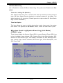
Chapter 4 BIOS
4-1
Introduction....................................................................................................... 4-1
System BIOS.................................................................................................... 4-1
How To Change the Configuration Data.......................................................... 4-1
4-2
Running Setup................................................................................................. 4-2
4-3
Main BIOS Setup............................................................................................. 4-2
Main BIOS Setup Menu................................................................................... 4-3
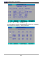
4-4
Advanced Setup............................................................................................... 4-6
4-5
Security Settings............................................................................................ 4-22
4-6
Boot Settings.................................................................................................. 4-24
4-7
Exit................................................................................................................. 4-25
Appendix A BIOS POST Error Codes
Appendix B Installing the Windows OS
Appendix C Installing Other Software Programs and Driver
viii
Chapter 1: Introduction
Chapter 1
Introduction
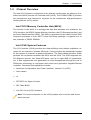
1-1 Overview
Checklist
Congratulations on purchasing your computer motherboard from an acknowledged
leader in the industry. Supermicro boards are designed with the utmost attention to
detail to provide you with the highest standards in quality and performance. Check
that the following items have all been included with your motherboard. If anything
listed here is damaged or missing, contact your retailer.
All the following items are included in the retail box.
•One (1) Supermicro Mainboard
•One (1) floppy cable (CBL-0022L)
•Six (6) SATA cables (CBL-0044L)
•One (1) I/O shield (MCP-260-00027- 0N)
•One (1) Supermicro CD containing drivers and utilities
•One (1) User's/BIOS Manual (MNL-1038)
1-1
X7SB3/X7SB3-F User's Manual
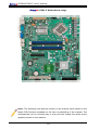
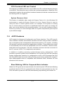
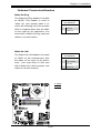
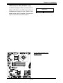
X7SB3-F Motherboard Image
Note: The drawings and pictures shown in this manual were based on the
latest PCB Revision available at the time of publishing of the manual. The
motherboard you’ve received may or may not look exactly the same as the
graphics shown in the manual.
1-2
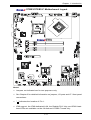
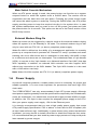
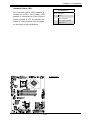
Chapter 1: Introduction
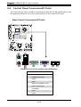
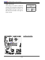
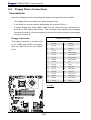
X7SB3/X7SB3-F Motherboard Layout
24-pin ATX PWR
KB/MOUSE
PW4
JAR
J3P
JPW2
JPW1
IPMI LAN
(X7SB3-F)
USB0/1
8-pin PWR
Fan1
JPUSB1
Intel
CPU
3210 MCH
COM1 JPL1
(North Bridge)
Intel
82574L
LAN
CTRL1
X7SB3
DIMM1
DIMM1A
JLED1
FP CTRL
JLAN2
DIMM2A
DIMM2
DIMM3
LE1
JPF
DIMM1B
DIMM2B
Fan5
JF1
JLAN1
VGA
DIMM4
JPL2
Fan2
LE2
BIOS
WPCM450-R
JWD
JBT1
(South Bridge)
3-SGPIO2
JL1
J27
SAS7
USB2
SAS6
SAS4
SAS1
SAS0
I-SATA1
I-Button
Fan4
JS1
JWOL
USB6/7
J45
JI2C1
USB4/5
J44
JD1
COM2
PCI1
SPKR1
PCI 33 MHz
JI2C2
JS2
I-SATA0
3-SGPIO1
B1
SAS5
LE3
LE4
Battery
J47
JPS2
Winbond
83627DHG
SI/O
LED1
Floppy
ICH9
JWOR
JPS1
LE5
J48
SAS CTRL
USB3
LSI
1068E
Intel
JPB
SAS3
IPMI/VGA CTRL
SAS2
Winbond
JPG1
Fan3
PCI-E x8
J8
Intel
82574L
LAN
CTRL2
Notes:
•Jumpers not indicated are for test purposes only.
•See Chapter 2 for detailed information on jumpers, I/O ports and JF1 front panel
connections.
•"
" indicates the location of Pin 1.
•IPMI support, the IPMI-dedicated LAN, the Realtek PHY chip, and IPMI Heartbeat LEDs are available on the full-featured X7SB3-F board only.
1-3
X7SB3/X7SB3-F User's Manual
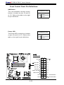
X7SB3/X7SB3-F Quick Reference
1
24-pin ATX PWR
JPUSB1
3
61
60
J3P
JAR
58
59
8-pin PWR
Fan1
JPW2
Intel
CPU
3210 MCH
COM1 JPL1
(North Bridge)
Intel
82574L
LAN
CTRL1
JLAN1
VGA
DIMM1A
JLED1
DIMM2A
JLAN2
7
X7SB3
DIMM1
FP CTRL
6
DIMM2
DIMM3
DIMM2B
Fan5
11
LE2
Winbond
BIOS
WPCM450-R
JWD
(South Bridge)
JS1
JS2
JWOL
USB6/7
J27
SAS7
USB2
SAS6
SAS0
I-Button
46
45
44
Fan4
20 21
JI2C1
USB4/5
J45
JD1
J44
19
COM2
PCI1
SPKR1
PCI 33 MHz
JI2C2
I-SATA1
3-SGPIO1
B1
SAS4
LE3
LE4
3-SGPIO2
I-SATA0
17
18
Battery
J47
JPS2
Winbond
83627DHG
SI/O
LED1
Floppy
ICH9
JWOR
JPS1
LE5
J48
SAS CTRL
USB3
LSI
1068E
Intel
JPB
SAS5
JPG1
51
50
49
48
47
JBT1
IPMI/VGA CTRL
SAS3
12
13
14
15
16
Fan3
PCI-E x8
56
54
53
52
Fan2
Intel
82574L
LAN
CTRL2
57
55
JPL2
SAS1
10
DIMM4
J8
9
LE1
JPF
DIMM1B
8
JF1
5
SAS2
4
62
PW4
JPW1
IPMI LAN
(X7SB3-F)
USB0/1
2
63
64
KB/MOUSE
JL1
22 23 24 2526 27 28 29303132 33 3435 36 37 38 39 40 41 42 43
Jumper
Label Description
Default Setting
JBT1
12
(See Chapter 2)
JI2C1/JI2C2
21/23 SMB to PCI slots Enable
Off (Disabled)
JPF
55
Power Force-On
Off (Normal)
JPG1
13
(BMC) VGA Enable
Pins 1-2 (Enabled)
JPL1/JPL2
4/9
LAN1/2 Enable/Disable
Pins 1-2 (Enabled)
JPS1
47
SAS Enable/Disable
Pins 1-2 (Enabled)
JPS2
31
SAS ID/RAID Mode Select
Closed (Software RAID)
JPUSB1
64
BP USB Wake-up Enable
Pins 1-2 (Enabled)
JWD
49
Watch Dog
Pins 1-2 (Reset)
CMOS Clear
1-4
Chapter 1: Introduction
Connector
Label
Description
B1
17
Onboard Battery
BIOS Chip
15
Phoenix SPI BIOS Chip
COM1/COM2
3/22
COM1/COM2 Serial Port/Header
Fan1:59,Fan2: 53,
Fans 1~5
Fan3:52,Fan4: 43, Fans 1~5: Chassis/CPU/System Fans
Fan5: 8
Floppy
46
Floppy Drive Connector
I-Button
45
I-Button Socket
J3P (Optional)
61
Redundant PWR Fail Detect (for internal use)
IPMI LAN
2
Dedicated LAN for IPMI (X7SB3-F only)
JAR
60
JD1
20
JF1
56
Alarm Reset
Onboard Speaker Header (Pins 3~4: Internal
Buzzer, Pins 1~4: External Speaker)
Front Panel Control Connector
JL1
34
Chassis Intrusion Header
JLAN 1~2
6/7
Gigabit Ethernet (RJ45) Ports
JLED1
57
Onboard Power LED
JPW1
63
ATX Main Power Connector
JPW2
58
12V 8-Pin Auxiliary PWR Connector
JWOL
26
Wake-On-LAN Header
JWOR
16
Wake-On-Ring Header
KB/MS
1
PS/2 Keyboard/Mouse
PW4 (X7SB3-F) 62
Power Supply SMB (I2C) Connector
SAS 0~7
35~42
Serial_Attached SCSI Connectors
(I-)SATA 0/1
29/30
(Intel South Bridge) Serial_ATA Ports 0~1
(3-)SGPIO 1/2
32/33
Serial-Link General Purpose I/O Headers
SPKR1
19
Internal Buzzer/Speaker
USB 0/1
2
Back Panel USB Ports#0~1
USB 2,USB 3
44/48
Front Panel Accessible USB Connectors 2~3
USB 4~5, 6~7
24/27
Front Panel USB Ports 4~5, 6~7
VGA
5
VGA Connector
LED
Label
Description
Status
LE1
54
Onboard Standby Power LED
Green: On (PWR On)
LE2
12
IPMI Heartbeat LED (X7SB3-F) Green: Blinking (IPMI Ready)
LE3/LE4
28/25
BIOS POST Codes LED
(Reserved for Internal Use)
LE5
51
SAS Heartbeat LED
Yellow: Blinking (SAS Ready)
LED1
50
SAS Activity LED
Green: Blinking (SAS Active)
Note: Jumper JPB (14) is used for factory debug puposes only.
1-5
X7SB3/X7SB3-F User's Manual
Motherboard Features
CPU
• Single Intel® Xeon® LGA 775 Quad-Core/Dual-Core 3000 Sequence or Core™
2 processor at a front side bus speed of 1333/1066/800 MHz
Memory
• Four 240-pin DIMM sockets with support of up to 8 GB ECC/Non-ECC Unbuffered DDR2 800/667 MHz Memory with DIMM size of 2 GB/1 GB/512 MB/256
MB @ 1.8V (See Section 2-4 in Chapter 2 for DIMM Slot Population.)
Chipset
• Intel® 3210 chipset, including: the 3210 Memory Control Hub (MCH), and the
ICH9 South Bridge
Expansion Slots
• One PCI-E x8 slot (J8) (Not for a graphics card)
• One PCI 33MHz slot (PCI1)
BIOS
• 16 Mb Phoenix® SPI Flash EEPROM
• DMI 2.3, PCI 2.2, APM 1.2, ACPI 1.0/2.0/3.0, Plug and Play (PnP), USB Keyboard support, and SMBIOS 2.3
PC Health Monitoring
• Onboard voltage monitors for CPU cores, Memory, Chipset, +1.8V, +3.3V, +5V,
+12V, -12V, +3.3V standby, Vcore and VBAT
• Fan status monitor with firmware control
• CPU/chassis temperature monitors
• CPU 4-phase switching voltage regulator
• CPU slow-down on temperature overheat
• CPU thermal trip support for processor protection
• Thermal Monitor 2 (TM2) support
• CPU fan auto-off in sleep mode
• PECI Ready (Platform Environment Control Interface)
• Low noise fan speed control
• Fan status monitor for on-off control
• Pulse Width Modulation (PWM) fan control
• Tachometer monitoring
• Power-up mode control for recovery from AC power loss
• Chassis intrusion detection
1-6
Chapter 1: Introduction
• System resource alert via Supero Doctor III
ACPI Features
• Slow blinking LED for suspend state indicator
• Main switch override mechanism
• ACPI Power Management
• Power-on mode for power recovery
Onboard I/O
• Two SATA ports
• Two Intel 82574L LAN chips support two Giga-bit LAN ports
• Additional IPMI-dedicated LAN supported by the Realtek RTL8201N
Ethernet
Controller (X7SB3-F only)
• One floppy port interface supports 1.44 MB
• Two COM ports(1 header, 1 port) supports Fast UART 16550 connection
• Up to eight USB 2.0 (Universal Serial Bus) (two backpanel connectors, two front
panel internal ports, and two Type A connectors)
• Super I/O: Winbond W83627DHG
• Winbond WPCM450-R Controller supports VGA and IPMI interface connections
(IPMI interface: X7SB3-F only)
Other
• External modem ring-on
• Wake-on-LAN (WOL)
• Wake-on-Ring (WOR)
• Console redirection
• Onboard Fan Speed Control by Thermal Management via BIOS
CD/Diskette Utilities
• Device drivers
Dimensions
• ATX 12.0" (L) x 9.6" (W) (304.8 mm x 243.8 mm)
1-7
X7SB3/X7SB3-F User's Manual
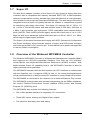
LGA775_PROCESSOR
VRM 11.0
CTRL
DATA
CTRL
DATA
DDR2_800/667
ADDR
DIMM_CHA/CHB
ADDR
FSB: 1333/1066/800MHz
Intel 3210
MCH
CK505 CLK
8 X SAS PORTS
PCIE_x8
PCIE_x8
LSI SAS 1068E
PCIE x8 SLOT
DMI
2 SATA PORTS
USB PORTS_0~7
PCI_32 SLOT
SPI FLASH 16Mb
S-ATA/300
USB 2.0/1.1
ICH9
PCI_32
NC-SI
PCIE_x1
GLAN1
82574L
RJ45
PCIE_x1
GLAN2
82574L
RJ45
PCI_32
SPI
LPC
LPC
WPCM450R
RMII
RTL8201N
PHY (X7SB3-F)
W83627DHG
LPC I/O
SER.1
SER.2
PS/2
KB/MS
FDD
VGA
PORT
RJ45
(X7SB3-F)
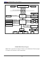
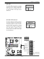
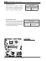
X7SB3/X7SB3-F Block Diagram
Note: This is a general block diagram. Please see the Motherboard Features pages
for details on the features of each motherboard.
1-8
Chapter 1: Introduction
1-2 Chipset Overview
The Intel 3210 chipset is comprised of two primary components: the Memory Controller Hub (MCH) and the I/O Controller Hub (ICH9). The X7SB3/X7SB3-F provides
the performance and feature-set required for the mainstream high-performance
cluster platform (HPC) market.
Intel 3210 Memory Controller Hub (MCH)
The function of the MCH is to manage the data flow between four interfaces: the
CPU interface, the DDR2 System Memory interface, the PCI Express interface, and
the Direct Media Interface (DMI). The MCH is optimized for the Intel® Xeon® 3000
Sequence processor in the LGA775 Land Grid Array package. It supports one or
two channels of DDR2 SDRAM.
Intel ICH9 System Features
The I/O Controller (ICH9) provides the data buffering and interface arbitration required for the system to operate efficiently. It also provides the bandwidth needed
for the system to maintain its peak performance. The Direct Media Interface (DMI)
provides the connection between the MCH and the ICH9. The ICH9 supports two
PCI-Express devices, two Serial ATA ports, and up to eight USB 2.0 ports/headers. It also supports the next generation of client management through the use of
PROActive technology in conjunction with Intel's next generation Gigabit Ethernet
controller. Functions and capabilities include:
•Advanced Configuration and Power Interface, Version 2.0 (ACPI)
•Power SMBus
•I C
2
•SST/PECI for Speed Control
•SPI Flash BIOS
•Low Pin Count (LPC) Interface
Note: For more information on the ICH9, please refer to Intel's web site at www.intel.com.
1-9
X7SB3/X7SB3-F User's Manual
1-3 Special Features
Recovery from AC Power Loss
BIOS provides a setting for you to determine how the system will respond when
AC power is lost and then restored to the system. You can choose for the system
to remain powered off (in which case you must hit the power switch to turn it
back on) or for it to automatically return to a power- on state. See the Power Lost
Control setting in the Advanced BIOS Setup section to change this setting. The
default setting is Last State.
1-4 PC Health Monitoring
This section describes the PC health monitoring features of the X7SB3/X7SB3-F.
All have an onboard System Hardware Monitor chip that supports PC health monitoring.
Voltage Monitoring
An onboard voltage monitor will scan the CPU Core, Chipset, +1.8V, +3.3V, +5V,
+12V, -12V, +3.3V Standby, +5V Standby and VBAT voltages continuously. Once
a voltage becomes unstable, a warning is given or an error message is sent to
the screen. Users can adjust the voltage thresholds to define the sensitivity of the
voltage monitor.
Fan Status Monitor with Firmware Control
The PC health monitor can check the RPM status of the cooling fans. The onboard
CPU and chassis fans are controlled by Thermal Management via BIOS (under
Hardware Monitoring in the Advanced Setting).
Environmental Temperature Control
The thermal control sensor monitors the CPU temperature in real time and will turn
on the thermal control fan whenever the CPU temperature exceeds a user-defined
threshold. The overheat circuitry runs independently from the CPU. Once it detects
that the CPU temperature is too high, it will automatically turn on the thermal fan
control to prevent any overheat damage to the CPU. The onboard chassis thermal
circuitry can monitor the overall system temperature and alert users when the chassis temperature is too high.
1-10
Chapter 1: Introduction
CPU Overheat LED and Control
This feature is available when the user enables the CPU overheat warning function
in the BIOS. This allows the user to define an overheat temperature. When the CPU
temperature reaches the pre-defined overheat threshold, both the overheat fan and
the warning LED are triggered.
System Resource Alert
This feature is available when used with Supero Doctor III in the Windows OS
environment or used with Supero Doctor II in Linux. Supero Doctor is used to
notify the user of certain system events. For example, if the system is running
low on virtual memory and there is insufficient hard drive space for saving the
data, you can be alerted of the potential problem. You can also configure Supero
Doctor to provide you with warnings when the system temperature goes beyond
a pre-defined range.
1-5 ACPI Features
ACPI stands for Advanced Configuration and Power Interface. The ACPI specification defines a flexible and abstract hardware interface that provides a standard
way to integrate power management features throughout a PC system, including
its hardware, operating system and application software. This enables the system
to automatically turn on and off peripherals such as CD-ROMs, network cards,
hard disk drives and printers. This also includes consumer devices connected to
the PC such as VCRs, TVs, telephones and stereos.
In addition to enabling operating system-directed power management, ACPI
provides a generic system event mechanism for Plug and Play and an operating
system-independent interface for configuration control. ACPI leverages the Plug
and Play BIOS data structures while providing a processor architecture-independent implementation that is compatible with Windows 2000, Windows XP and
Windows 2003 Servers.
Slow Blinking LED for Suspend-State Indicator
When the CPU goes into a suspend state, the chassis power LED will start blinking
to indicate that the CPU is in suspend mode. When the user presses any key, the
CPU will wake-up and the LED will automatically stop blinking and remain on.
1-11
X7SB3/X7SB3-F User's Manual
Main Switch Override Mechanism
When an ATX power supply is used, the power button can function as a system
suspend button to make the system enter a SoftOff state. The monitor will be
suspended and the hard drive will spin down. Pressing the power button again
will cause the whole system to wake-up. During the SoftOff state, the ATX power
supply provides power to keep the required circuitry in the system alive. In case
the system malfunctions and you want to turn off the power, just press and hold
the power button for 4 seconds. This option can be set in the Power section of the
BIOS Setup routine.
External Modem Ring-On
Wake-up events can be triggered by a device such as the external modem ringing
when the system is in the Standby or Off state. The external modem ring-on can
only be used with an ATX 2.01 (or above) compliant power supply.
Wake-On-LAN is defined as the ability of a management application to remotely
power up a computer that is powered off. Remote PC setup, up-dates and asset
tracking can occur after hours and on weekends so that daily LAN traffic is kept
to a minimum and users are not interrupted. The motherboard has a 3-pin header
(WOL) to connect to the 3-pin header on a Network Interface Card (NIC) that has
WOL capability. In addition, an onboard LAN controller can also support WOL
without any connection to the WOL header. The 3-pin WOL header is to be used
with a LAN add-on card only.
Note: Wake-On-LAN requires an ATX 2.01 (or above) compliant power supply.
1-6 Power Supply
As with all computer products, a stable power source is necessary for proper and
reliable operation. It is even more important for processors that have high CPU
clock rates.
The X7SB3/X7SB3-F can only accommodate 24-pin ATX power supply. Although
most power supplies generally meet the specifications required by the motherboard,
some are inadequate. You should use one that will supply at least 400W of power.
In addition, the 12V 8-pin is also required for adequate power supply to the CPU.
Also your power supply must supply 1.5A for the Ethernet ports.
It is strongly recommended that you use a high quality power supply that meets
ATX power supply Specification 2.02 or above. It must also be SSI compliant (info
at http://www.ssiforum.org/). Additionally, in areas where noisy power transmission
is present, you may choose to install a line filter to shield the computer from noise.
It is recommended that you also install a power surge protector to help avoid problems caused by power surges.
1-12
Chapter 1: Introduction
1-7 Super I/O
The disk drive adapter functions of the Super I/O chip include a floppy disk drive
controller that is compatible with industry standard 82077/765, a data separator,
write pre-compensation circuitry, decode logic, data rate selection, a clock generator,
drive interface control logic and interrupt and DMA logic. The wide range of functions
integrated onto the Super I/O greatly reduces the number of components required
for interfacing with floppy disk drives. The Super I/O supports 360 K, 720 K, 1.2
M, 1.44 M or 2.88 M disk drives and data transfer rates of 250 Kb/s, 500 Kb/s or
1 Mb/s. It also provides two high-speed, 16550 compatible serial communication
ports (UARTs). Both UARTs provide legacy speed with baud rate of up to 115.2
Kbps as well as an advanced speed with baud rates of 250 K, 500 K, or 1 Mb/s,
which support higher speed modems.
The Super I/O provides functions that comply with ACPI (Advanced Configuration
and Power Interface), which includes support of legacy and ACPI power management through an SMI or SCI function pin. It also features auto power management
to reduce power consumption.
1-8 Overview of the Winbond WPCM450 Controller
The Winbond WPCM450 Controller is a Baseboard Management Controller (BMC)
that supports the 2D/VGA-compatible Graphics Core with the PCI interface,
Virtual Media, and Keyboard/Video/Mouse Redirection (KVMR) modules. With
blade-oriented Super I/O capability built-in, the WPCM450 Controller is ideal for
legacy-reduced server platforms.
The WPCM450 interfaces with the host system via a PCI interface to communicate
with the Graphics core. It supports USB 2.0 and 1.1 for remote keyboard/mouse/
virtual media emulation. It also provides LPC interface to control Super IO functions.
The WPCM450 is connected to the network via an external Ethernet Phy module.
The WPCM450 communicates with onboard components via six SMBus interfaces,
fan control, Platform Environment Control Interface (PECI) buses, and General
Purpose I/O (3SGPIO) ports.
The WPCM450 also includes the following features:
•One X-Bus parallel interface for expansion I/O connections
•Three ADC inputs, Analog and Digital Video outputs
•Two serial for boundary scan and debug
1-13
X7SB3/X7SB3-F User's Manual
Notes
1-14
Chapter 2: Installation
Chapter 2
Installation
2-1 Static-Sensitive Devices
Electro-Static-Discharge (ESD) can damage electronic components. To prevent
damage to your system board, it is important to handle it very carefully. The following
measures are generally sufficient to protect your equipment from ESD.
Precautions
•Use a grounded wrist strap designed to prevent static discharge.
•Touch a grounded metal object before removing the board from the antistatic
bag.
•Handle the board by its edges only; do not touch its components, peripheral
chips, memory modules or gold contacts.
•When handling chips or modules, avoid touching their pins.
•Put the motherboard and peripherals back into their antistatic bags when not
in use.
•For grounding purposes, make sure your computer chassis provides excellent
conductivity between the power supply, the case, the mounting fasteners and
the motherboard.
•Use
only the correct type of onboard CMOS battery as specified by the
manufacturer. Do not install the onboard battery upside down to avoid possible
explosion.
Unpacking
The motherboard is shipped in antistatic packaging to avoid static damage. When
unpacking the board, make sure the person handling it is static protected.
2-1
X7SB3/X7SB3-F User's Manual
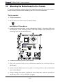
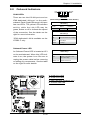
2-2 Mounting the Motherboard in the Chassis
For proper installation, please follow the instructions below to mount the motherboard into the chassis before installing the CPU on the motherboard.
Tools needed
•Phillips screwdriver
•#6 32 x5mm pan head screw as shown below.
Pan head
Installation
Procedures
6-32 x 5 mm
•Locate
[0.197]the mounting holes on the motherboard. Refer to the layout below for
the locations of the mounting holes. (The holes marked with arrows are the
mounting holes on this motherboard.)
X7SB3
•Locate the mounting holes on the chassis.
•Align the mounting holes on the motherboard against the mounting holes on
the chassis.
•Insert a #6 pan head screw into a pair of mounting holes on the motherboard
and on the chassis.
•Using a Phillips screwdriver, tighten the screw. Make sure that the standoffs on
the chassis click in or are screwed in tightly.
2-2
Chapter 2: Installation
•Repeat the step above until the motherboard is securely installed into the
chassis.
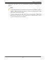
Notes
1. All motherboards have standard mounting holes to fit different types of
chassis. Make sure that the locations of all the mounting holes for both
motherboard and chassis match.
2. Some components are very close to the mounting holes. Please take
precautionary measures to avoid damaging the components when installing the motherboard into the chassis.
2-3
X7SB3/X7SB3-F User's Manual
2-3 Installing the Processor and Heatsink Fans
!
Warning: When handling the processor package, avoid placing
direct pressure on the label area of the fan.
Notes:
1. Always connect the power cord last and always remove it before adding,
removing or changing any components. Make sure that you install the processor into the CPU socket before you install the CPU heatsink.
2. Intel's boxed Xeon® CPU package contains the CPU fan and heatsink assembly. If you buy a CPU separately, make sure that you use only Intel-certified multi-directional heatsink and fan.
3. Make sure to install the motherboard into the chassis before you install the
CPU heatsink and fan.
4. When purchasing a motherboard with an LGA 775 CPU Socket, make sure
that the CPU plastic cap is in place, and none of the CPU Socket pins are
bent; otherwise, contact the retailer immediately.
5. Refer to the Chipset/MB Features Section for more details on CPU support.
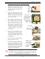
Installing the LGA775 Processor
1. Press the load lever to release
the load plate, which covers the
CPU socket, from its locking
position.
PnP Cap on
top of the
Load Plate
Load Lever
2. Gently lift the load lever to open
the load plate.
3. Use your thumb and your index
finger to hold the CPU at the
North Center Edge and the South
Center Edge of the CPU.
Load Plate
(with PnP Cap
attached)
2-4
Chapter 2: Installation
Loading the Processor into the Socket
1. Align CPU Pin1 (the CPU corner
marked with a triangle) against the
socket corner that is marked with a
triangle cutout.
2. Align the CPU key that is the
semi-circle cutout below a gold dot
against the socket key, the notch
on the same side of the triangle
cutout on the socket.
3. Once aligned, carefully lower the
CPU straight down to the socket.
(Do not drop the CPU on the
socket. Do not move the CPU
horizontally or vertically. Do not
rub the CPU against the surface
or against any pins of the socket
to avoid damage to the CPU or
the socket.)
North
Center
Edge
South
Center
Edge
gold dot
Socket Key
(Socket Notch)
CPU Key (semicircle cutout)
below the circle.
Corner with a
triangle cutout
CPU Pin1
Load Lever
CPU in the
CPU socket
4. With the CPU installed in the
socket, inspect the four corners of
the CPU to make sure that the CPU
is properly installed. Then, close
the load plate.
5. Use your thumb to gently push the
load lever down to lock it.
6. If the CPU is properly installed into
the socket, the plastic cap will be
automatically released from the
load plate when the clip is pushed
in the clip lock. Remove the plastic
cap from the motherboard.
!
Plastic cap is
released from
the load plate
if the CPU
properly installed.
Warning: Please save the plastic PnP cap. The motherboard must
be shipped with the PnP cap properly installed to protect the CPU
socket pins. Shipment without the PnP cap properly installed will
cause damage to the socket pins.
2-5
X7SB3/X7SB3-F User's Manual
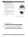
Installing the Heatsink
1. Do not apply any thermal grease to the
heatsink or the CPU die; the required
amount has already been applied.
2. Place the heatsink on top of the CPU
so that the four mounting holes are
aligned with those on the retention
mechanism.
UP Passive Heatsink
Screw#1
Screw#2
3. Screw in two diagonal screws (ie the #1
and the #2 screws) until just snug (-do
not fully tighten the screws to avoid
possible damage to the CPU.)
4. Finish the installation by fully tightening
all four screws.
Screw#1
Removing the Heatsink
!
Warning: We do not recommend that the CPU or the heatsink be
removed. However, if you do need to uninstall the heatsink, please
follow the instructions on the next page to uninstall the heatsink to
prevent damage done to the CPU or the CPU socket.
2-6
Screw#2
Chapter 2: Installation
1. Unscrew and remove the heatsink
screws from the motherboard in the
sequence as shown in the picture on
the right.
2. Hold the heatsink as shown in the picture on the right and gently wriggle the
heatsink to loosen it from the CPU. (Do
not use excessive force when wriggling
the heatsink!!)
3. Once the heatsink is loosened, remove
the heatsink from the CPU socket.
4. Clean the surface of the CPU and the
heatsink to get rid of the old thermal
grease. Reapply the proper amount
of thermal grease on the surface before you re-install the CPU and the
heatsink.
2-7
Screw#1
Screw#2
X7SB3/X7SB3-F User's Manual
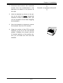
2-4 Installing DIMMs
CAUTION
Exercise extreme care when installing or removing DIMM
modules to prevent any possible damage. Also note that the
memory is interleaved to improve performance..
DIMM Installation
1. Insert the desired number of DIMMs into the memory slots, starting with
DIMM #1A, #1B, then #2A and #2B.
2. Insert each DIMM module vertically into its slot. Gently press down on the
DIMM module until it snaps into place in the slot. Repeat for all modules. Pay
attention to the notch along the bottom of the module to prevent inserting the
DIMM module incorrectly.
3. This motherboard supports both dual-rank and single-rank memory modules.
For system memory to work properly, please use all dual-rank memory modules or use all single-rank memory modules on the same motherboard. Check
the Supermicro web site for other information.
Memory Support
The X7SB3/X7SB3-F supports up to 8 GB Unbuffered ECC/Non-ECC DDR2
800/667 MHz in 4 DIMMs. Populating memory slots of the same bank with a pair
(or pairs) of memory modules of the same size and same type will result in twoway Interleaved Memory which will improve memory performance. (See the table
below.)
No. of
DIMMs
2 DIMMs
4 DIMMs
Optimized DIMM Population Configurations
Channel 0
DIMM#1A
DIMM#1A
-----DIMM#2A
Channel 1
DIMM#1B
DIMM#1B
-----DIMM#2B
(Notes: i. DIMM slot# specified: DIMM slot to be populated; “---“: DIMM slot not to be
populated. ii. DDR2 ECC/Non-ECC Unbuffered 800 MHz/667 MHz DIMMs are supported;
however, please use the memory modules of the same speed and of the same type on a
motherboard. iii. For memory to work properly, you need to follow the restrictions listed
above. )
Note 1: Due to OS limitations, some operating systems may not show
more than 4 GB of memory.
Note 2: Due to memory allocation to system devices, memory remaining
available for operational use will be reduced when 4 GB of RAM is used.
2-8
Chapter 2: Installation
Possible System Memory Allocation & Availability
System Device
Size
Physical Memory
Remaining (-Available)
(4 GB Total System Memory)
Firmware Hub flash memory (System BIOS)
1 MB
3.99
Local APIC
4 KB
3.99
Area Reserved for the chipset
2 MB
3.99
I/O APIC (4 Kbytes)
4 KB
3.99
PCI Enumeration Area 1
256 MB
3.76
PCI Express (256 MB)
256 MB
3.51
PCI Enumeration Area 2 (if needed) -Aligned on 256MB boundary-
512 MB
3.01
VGA Memory
16 MB
2.85
TSEG
1 MB
2.84
Memory available to OS and other applications
2.84
Installing and Removing DIMMs
DDR2 DIMM
Notch
Notch
X7SB3
Note: Notch
should align
with the
receptive point
on the slot
Release
Tab
Release
Tab
To Install: Insert module vertically and press
down until it snaps into place. Pay attention to the
alignment notch at the bottom.
To Remove:
Use your thumbs to
gently push the release tabs near both
ends of the module
to release it from the
slot.
Top View of DDR2 ECC Slot
Release Tab
Release Tab
2-9
X7SB3/X7SB3-F User's Manual
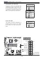
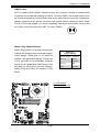
2-5 Control Panel Connectors/IO Ports
The I/O ports are color coded in conformance with the PC 99 specification. See
the graphics below for the colors and locations of the various I/O ports.
Back Panel Connectors/IO Ports
X7SB3
2
1
5
4
6
7
8
9
3
Back Panel I/O Port Locations and Definitions
Back Panel Connectors
1
Keyboard (Purple)
2
PS/2Mouse (Green)
3
USB 0
4
USB 1
5
IPMI LAN (X7SB3-F only)
6
COM 1 (Turquoise)
7
VGA (Blue)
8
LAN 1
9
LAN 2
(See Section 2-6 for details.)
2-10
Chapter 2: Installation
Front Control Panel
JF1 contains header pins for various buttons and indicators that are normally located on a control panel at the front of the chassis. These connectors are designed
specifically for use with Supermicro server chassis. See the figure below for the
descriptions of the various control panel buttons and LED indicators. Refer to the
following section for descriptions and pin definitions.
Front Control Panel Header (JF1) Pins
20 19
X7SB3
2 1
20
19
Ground
NMI
X
X
Vcc
Power LED
Vcc
HDD LED
Vcc
NIC1 LED
NIC2 LED
Vcc
OH/Fan Fail LED
Vcc
PWR Fail LED
Vcc
Ground
Ground
2
2-11
1
Reset
Reset Button
PWR
Power Button
X7SB3/X7SB3-F User's Manual
Front Control Panel Pin Definitions
NMI Button
NMI Button
Pin Definitions (JF1)
The non-maskable interrupt button
header is located on pins 19 and 20
of JF1. Refer to the table on the right
for pin definitions.
Power LED
Pin#
Definition
19
Control
20
Ground
Power LED
Pin Definitions (JF1)
The Power LED connection is located
on pins 15 and 16 of JF1. Refer to the
table on the right for pin definitions.
Pin#
Definition
15
Vcc
16
Ground
A. NMI
B. PWR LED
20
19
Ground
NMI
X
X7SB3
B Power LED
Vcc
HDD LED
Vcc
NIC1 LED
Vcc
NIC2 LED
Vcc
Vcc
OH/Fan Fail LED
Vcc
PWR Fail LED
Ground
Ground
2
2-12
A
X
1
Reset
FP Reset Button
PWR
FP Power Button
Chapter 2: Installation
HDD LED
HDD/UID LED
Pin Definitions (JF1)
The HDD LED connection is located
on pin 14 of JF1. Attach a hard-drive
LED cable here to display disk activity. See the table on the right for pin
definitions.
Pin#
Definition
13
Vcc
14
HD Active
NIC1/NIC2 LED Indicators
The NIC (Network Interface Controller) LED connection for GLAN port1
is located on pins 11 and 12 of JF1
and the LED connection for GLAN
Port2 is on Pins 9 and 10. Attach the
NIC LED cables to display network
activity. Refer to the table on the right
for pin definitions.
GLAN1/2 LED
Pin Definitions (JF1)
Pin#
Definition
9/11
Vcc
10/12
NIC LED
A. HDD LED
B. NIC1 LED
C. NIC2 LED
20
19
Ground
NMI
X
X7SB3
X
Vcc
Power LED
A
HDD LED
Vcc
B
NIC1 LED
Vcc
C
NIC2 LED
Vcc
Vcc
OH/Fan Fail LED
Vcc
PWR Fail LED
Ground
Ground
2
2-13
1
Reset
FP Reset Button
PWR
FP Power Button
X7SB3/X7SB3-F User's Manual
Overheat/Fan Fail LED (OH)
OH/Fan Fail LED
Pin Definitions (JF1)
Connect an LED to the OH/Fan Fail
connection on pins 7 and 8 of JF1 to
provide advanced warnings of chassis
overheating or fan failure. Refer to the
table on the right for pin definitions.
Pin#
Definition
7
Vcc
8
OH/Fan Fail
OH/Fan Fail Indicator
Status
State
Power Fail LED
Definition
Off
Normal
On
Overheat
Flashing
Fan Fail
PWR Fail LED
Pin Definitions (JF1)
The Power Fail LED connection is
located on pins 5 and 6 of JF1. Refer
to the table on the right for pin definitions.
Pin#
Definition
5
Vcc
6
Power Fail
A. OH/Fan Fail LED
B. PWR Supply Fail
20
19
Ground
NMI
X
X7SB3
X
Power LED
Vcc
HDD LED
Vcc
NIC1 LED
Vcc
NIC2 LED
Vcc
A OH/Fan Fail LED
B
Vcc
Vcc
PWR Fail LED
Ground
Ground
2
2-14
1
Reset
FP Reset Button
PWR
FP Power Button
Chapter 2: Installation
Reset Button
Reset Button
Pin Definitions (JF1)
The Reset Button connection is located
on pins 3 and 4 of JF1. Attach it to the
hardware reset switch on the computer
case. Refer to the table on the right for
pin definitions.
Pin#
Definition
3
Reset
4
Ground
Power Button
The Power Button connection is located
on pins 1 and 2 of JF1. Momentarily
contacting both pins will power on/off
the system. This button can also be
configured to function as a suspend
button (with a setting in the BIOS - see
Chapter 4). To turn off the power when
set to suspend mode, press the button
for at least 4 seconds. Refer to the table
on the right for pin definitions.
Power Button
Pin Definitions (JF1)
Pin#
Definition
1
Power On
2
Ground
A. Reset Button
B. PWR Button
20
19
Ground
NMI
X
X7SB3
X
Power LED
Vcc
HDD LED
Vcc
NIC1 LED
Vcc
NIC2 LED
Vcc
Vcc
OH/Fan Fail LED
Vcc
PWR Fail LED
Ground
Ground
2
2-15
1
Reset
FP Reset Button A
PWR
FP Power ButtonB
X7SB3/X7SB3-F User's Manual
2-6 Connecting to the Headers and Connectors
Power Connectors
ATX Power 24-pin Connector
Pin Definitions
ATX Power Connector
A 24-pin main power supply connector
(JPW1) and an 8-pin CPU PWR connector
(JPW2) are located on the motherboard.
These power connectors meet the SSI
EPS 12V specification. For the 8-pin PWR
(JPW2), please refer to the item listed
below. See the table on the right for pin
definitions.
Processor Power Connector
In addition to the Primary ATX power connector (above), the 12V 8-pin CPU PWR
connector at JPW2 must also be connected
to your power supply. See the table on the
right for pin definitions.
Pin#
Definition
13
+3.3V
Pin #
1
+3.3V
Definition
14
-12V
2
+3.3V
15
COM
3
COM
16
PS_ON
4
+5V
17
COM
5
COM
18
COM
6
+5V
19
COM
7
COM
20
Res (NC)
8
PWR_OK
21
+5V
9
5VSB
22
+5V
10
+12V
23
+5V
11
+12V
24
COM
12
+3.3V
Required Connection
12V 8-pin Power CPU
Connector
Pin Definitions
Pins
Definition
1 through 4
Ground
5 through 8
+12V
Required Connections
A
24-pin ATX PWR
KB/MOUSE
PW4
A. 24-pin ATX PWR
JAR
J3P
JPW2
JPW1
IPMI LAN
(X7SB3-F)
USB0/1
B
8-pin PWR
Fan1
JPUSB1
Intel
B. 8-pin Processor PWR
CPU
3210 MCH
COM1 JPL1
(North Bridge)
Intel
82574L
LAN
CTRL1
X7SB3
DIMM1
DIMM1A
JLED1
FP CTRL
JLAN2
DIMM2A
DIMM2
DIMM3
LE1
JPF
DIMM1B
DIMM2B
Fan5
JF1
JLAN1
VGA
DIMM4
JPL2
Fan2
LE2
BIOS
JWD
JBT1
(South Bridge)
J48
J47
J27
SAS7
USB2
SAS6
SAS4
SAS0
JL1
I-Button
Fan4
JS1
JWOL
USB6/7
J45
JI2C1
USB4/5
J44
JD1
COM2
PCI1
SPKR1
PCI 33 MHz
I-SATA1
3-SGPIO1
B1
SAS5
LE3
3-SGPIO2
I-SATA0
Battery
JI2C2
LED1
JPS2
JS2
LE4
83627DHG
SI/O
USB3
SAS CTRL
ICH9
JWOR
Winbond
SAS1
JPB
JPS1
LE5
Floppy
LSI
1068E
Intel
SAS3
IPMI/VGA CTRL
SAS2
Winbond
WPCM450-R
JPG1
Fan3
PCI-E x8
J8
Intel
82574L
LAN
CTRL2
2-16
Chapter 2: Installation
Fan Headers
Fan Headers
The X7SB3/X7SB3-F has five system/chassis/CPU fan headers (Fans 1~Fan 5). These
fan headers support 4-pin or 3-pin fans.
However, for the system to function properly,
please use all 3-pin or all 4-pin fans on a
motherboard. See the table on the right for
pin definitions.
Note: The onboard fan speeds are
controlled by Thermal Management
via BIOS Hardware Monitoring in the
Advanced Setting. (The default setting
is Disabled.)
A
24-pin ATX PWR
KB/MOUSE
PW4
JAR
J3P
JPW2
JPW1
IPMI LAN
(X7SB3-F)
USB0/1
A. Fan 1
8-pin PWR
Fan1
JPUSB1
B. Fan 2
C. Fan 3
Intel
D. Fan 4
CPU
3210 MCH
COM1 JPL1
(North Bridge)
Intel
82574L
LAN
CTRL1
E. Fan 5
DIMM1A
JLED1
FP CTRL
JLAN2
DIMM2A
E
DIMM1B
LE1
JPF
Fan5
X7SB3
DIMM1
DIMM2
DIMM3
JF1
JLAN1
VGA
DIMM2B
DIMM4
B
JPL2
Fan2
LE2
BIOS
WPCM450-R
JWD
JBT1
(South Bridge)
J48
J47
J27
SAS7
SAS6
USB2
Fan4
SAS0
SAS1
I-SATA1
JL1
I-Button
SAS4
LE3
JS1
JWOL
USB6/7
J45
JI2C1
USB4/5
J44
JI2C2
COM2
PCI1
JD1
PCI 33 MHz
JS2
LE4
3-SGPIO1
B1
SPKR1
LED1
JPS2
3-SGPIO2
I-SATA0
Battery
USB3
SAS CTRL
ICH9
JWOR
Winbond
83627DHG
SI/O
JPS1
LE5
Floppy
LSI
1068E
Intel
SAS5
IPMI/VGA CTRL
SAS3
JPG1
JPB
SAS2
Winbond
C
Fan3
PCI-E x8
J8
Intel
82574L
LAN
CTRL2
D
2-17
Fan Header
Pin Definitions
Pin#
Definition
1
Ground
2
+12V
3
Tachometer
4
PWR Modulation
X7SB3/X7SB3-F User's Manual
I/O Connections
ATX PS/2 Keyboard and PS/2
Mouse Ports
PS/2 Keyboard and
Mouse Port Pin
Definitions
The ATX PS/2 keyboard and the PS/2
mouse are located on the I/O backplane. See the table on the right for pin
definitions. (The mouse port is above
the keyboard port.) See the table on
the right for pin definitions.
Serial Ports
24-pin ATX PWR
A
PW4
IPMI LAN
(X7SB3-F)
USB0/1
NC
3
Ground
4
VCC
5
Clock
6
NC
Pin #
Definition
Pin #
Definition
1
DCD
6
DSR
2
RXD
7
RTS
3
TXD
8
CTS
4
DTR
9
RI
5
Ground
10
NC
Pin 10 (Key) is available on
COM2 only. NC: No Connection.
JPW2
A. Keyboard/Mouse
Intel
B. COM1
CPU
3210 MCH
COM1 JPL1
C. COM2
(North Bridge)
Intel
82574L
LAN
CTRL1
X7SB3
DIMM1
DIMM1A
JLED1
FP CTRL
JLAN2
DIMM2A
DIMM2
DIMM3
LE1
JPF
DIMM1B
DIMM2B
Fan5
JF1
JLAN1
VGA
DIMM4
JPL2
Fan2
Fan3
J8
PCI-E x8
LE2
BIOS
JWD
JBT1
(South Bridge)
J48
J47
J27
SAS7
USB2
SAS6
SAS0
JL1
I-Button
Fan4
JS1
I-SATA0
JWOL
USB6/7
J45
JI2C1
USB4/5
J44
COM2
PCI1
JD1
PCI 33 MHz
SAS4
3-SGPIO1
C
B1
SAS5
LE3
3-SGPIO2
I-SATA1
Battery
JI2C2
LED1
JPS2
JS2
LE4
83627DHG
SI/O
USB3
SAS CTRL
ICH9
JWOR
Winbond
SAS1
JPB
JPS1
LE5
Floppy
LSI
1068E
Intel
SAS3
IPMI/VGA CTRL
SAS2
Winbond
WPCM450-R
SPKR1
2
JAR
J3P
JPW1
B
JPG1
Data
8-pin PWR
Fan1
JPUSB1
Intel
82574L
LAN
CTRL2
Definition
1
Serial Port Pin Definitions
COM1 and COM2 are serial port connections located on the motherboard.
COM1 is a connector located on the
I/O backplane. COM2 is a header located below PCI Slot 1 to provide front
access. See the table on the right for
pin definitions.
KB/MOUSE
Pin#
2-18
Chapter 2: Installation
Universal Serial Bus (USB)
Back Panel USB
(USB 0~1)
There are eight USB 2.0 (Universal Serial
Bus) ports/headers on the motherboard.
Two of them are Back Panel USB ports:
USB 0~1. The other six are front panel
accessible USB connections. USB 2 and
USB 3 are Type A connectors. USB 4~5,
and USB 6~7 are Front Panel Internal
Ports. See the tables on the right for pin
definitions.
Note: To comply with FCC requirements,
please do not attach an un-shielded cable
to a USB port, even if there is no device
attached to the cable. Use only a shielded
USB cable that meets the requirements for
a USB device.
Pin#
Definitions
1
+5V
2
PO-
3
PO+
4
Ground
5
N/A
Front Panel USB
Pin Definitions (USB 2~7)
USB 2/4/6/7
Pin #
Definition
USB 3/5
Pin #
Definition
1
+5V
1
+5V
2
PO-
2
PO-
3
PO+
3
PO+
4
Ground
4
Ground
5
No connection
5
Key
GLAN 1/2 Ethernet Ports and IPMIdedicated LAN Port
Two Ethernet ports are located on the I/O
backplane. These ports accept RJ45 type
cables. LAN 1/2 are G-bit LAN ports supported by the Intel 82574L controller. The
IPMI LAN located above USB ports on
the X7SB3-F is supported by the Realtek
RTL8201N Controller. (IPMI-dedicated
LAN is available on the X7SB3-F only.).
24-pin ATX PWR
A
KB/MOUSE
IPMI LAN
(X7SB3-F)
USB0/1
PW4
JAR
J3P
H
B. USB 2
JPW2
JPW1
C. USB 3
Intel
D. USB 4/5
CPU
3210 MCH
COM1 JPL1
(North Bridge)
Intel
82574L
LAN
CTRL1
DIMM1A
G
JLAN2
F. LAN Port 1
X7SB3
DIMM1
JLED1
DIMM2A
DIMM2
DIMM3
LE1
JPF
DIMM1B
DIMM2B
Fan5
JF1
JLAN1
F
E. USB 6/7
FP CTRL
VGA
DIMM4
JPL2
Fan2
LE2
BIOS
JWD
JBT1
(South Bridge)
J47
C
B
J27
SAS7
USB2
SAS6
SAS4
SAS0
SAS1
I-SATA1
JL1
I-Button
SAS5
LE3
JWOL
USB6/7
JS1
I-SATA0
LE4
JI2C1
USB4/5
E
JS2
JI2C2
3-SGPIO1
Fan4
JD1
J44
SPKR1
D
PCI 33 MHz
COM2
PCI1
B1
LED1
JPS2
3-SGPIO2
J45
Battery
J48
ICH9
JWOR
Winbond
83627DHG
SI/O
JPS1
LE5
USB3
SAS CTRL
Floppy
LSI
1068E
Intel
JPB
SAS3
IPMI/VGA CTRL
SAS2
Winbond
WPCM450-R
JPG1
Fan3
PCI-E x8
J8
Intel
82574L
LAN
CTRL2
F
A. USB 0/1
8-pin PWR
Fan1
JPUSB1
H
2-19
G. LAN Port 2
H. IPMI LAN (X7SB3-F only)
G
X7SB3/X7SB3-F User's Manual
VGA Connector
A VGA connector is located next to
COM1 port on the IO backplane.
This Video port is supported by the
Winbond Hermon-R chip. Refer to
the board layout below for the location.
Serial ATA Ports
Two Serial ATA (SATA) ports
(SATA0~SATA1) are located at
JS1~JS2 on the motherboard. Additional four SATA ports located at
JS3~JS6 are optional. These SATA
connections are supported by Intel
South Bridge to provide Serial-Link
signal transmissions on the motherboard. See the table on the right for
pin definitions. Refer to the board
layout below for the locations of the
headers.
24-pin ATX PWR
KB/MOUSE
PW4
IPMI LAN
(X7SB3-F)
USB0/1
JAR
J3P
CPU
COM1 JPL1
(North Bridge)
Intel
82574L
LAN
CTRL1
X7SB3
DIMM1
DIMM1A
JLED1
FP CTRL
JLAN2
DIMM2A
DIMM2
DIMM3
LE1
JPF
DIMM1B
DIMM2B
Fan5
JF1
JLAN1
VGA
DIMM4
JPL2
Fan2
LE2
BIOS
JWD
JBT1
(South Bridge)
J48
J47
3-SGPIO2
J27
SAS7
USB2
SAS6
SAS4
I-Button
SAS5
SAS0
JL1
SAS1
I-SATA1
3-SGPIO1
Fan4
JWOL
USB6/7
JS2
LE3
LE4
JI2C1
USB4/5
JS1
JI2C2
J45
JD1
J44
SPKR1
PCI 33 MHz
COM2
PCI1
B1
LED1
JPS2
BC
I-SATA0
Battery
USB3
SAS CTRL
ICH9
JWOR
Winbond
83627DHG
SI/O
JPS1
LE5
Floppy
LSI
1068E
Intel
JPB
SAS3
IPMI/VGA CTRL
SAS2
Winbond
WPCM450-R
JPG1
Fan3
PCI-E x8
J8
Intel
82574L
LAN
CTRL2
Pin
Definition
Ground
2
TX+
3
TX-
4
Ground
5
RX-
6
RX+
7
Ground
C. SATA1
Intel
3210 MCH
A
Definition
1
B. SATA0
JPW2
JPW1
Pin#
A. VGA
8-pin PWR
Fan1
JPUSB1
SATA Port
Pin Definitions
2-20
Chapter 2: Installation
SAS Ports
Eight SAS (Serial-Attached SCSI)
ports (SAS0~SAS7) are located
SAS Port
Pin Definitions
below the LSI 1068E SAS Controller on the motherboard. These SAS
connections are supported by the
LSI 1068E Controller to provide
Serial-Link signal transmissions on
the motherboard. See the table on
the right for pin definitions. Refer to
the board layout below for the locations of the headers.
24-pin ATX PWR
KB/MOUSE
PW4
IPMI LAN
(X7SB3-F)
USB0/1
JAR
J3P
(North Bridge)
Intel
82574L
LAN
CTRL1
3
TX-
4
Ground
5
RX-
6
RX+
7
Ground
E. SAS4
F SAS5
X7SB3
DIMM1
DIMM1A
JLED1
FP CTRL
JLAN2
DIMM2A
DIMM2
DIMM3
LE1
JPF
DIMM1B
DIMM2B
Fan5
JF1
JLAN1
VGA
DIMM4
JPL2
Fan2
Fan3
J8
PCI-E x8
LE2
BIOS
JWD
JBT1
(South Bridge)
J48
J47
LE3
SAS7
SAS6
SAS4
SAS5
SAS0
JL1
SAS1
I-SATA1
F GUSB2
H J27
C D E
A B 3-SGPIO1
I-Button
Fan4
JS1
JS2
LE4
JWOL
USB6/7
J45
J44
JD1
PCI 33 MHz
COM2
PCI1
B1
JI2C1
USB4/5
LED1
JPS2
3-SGPIO2
I-SATA0
Battery
JI2C2
USB3
SAS CTRL
ICH9
JWOR
Winbond
83627DHG
SI/O
JPS1
LE5
Floppy
LSI
1068E
Intel
JPB
SAS3
IPMI/VGA CTRL
SAS2
Winbond
WPCM450-R
SPKR1
TX+
D. SAS3
CPU
COM1 JPL1
JPG1
Definition
2
C. SAS2
Intel
3210 MCH
Intel
82574L
LAN
CTRL2
Pin
Ground
B. SAS1
JPW2
JPW1
Definition
1
A. SAS0
8-pin PWR
Fan1
JPUSB1
Pin#
2-21
G SAS6
H. SAS7
X7SB3/X7SB3-F User's Manual
3-SGPIO Headers
Two Serial-Link General Purpose
Input/Output headers are located
between the SAS Controller and
the SAS ports on the motherboard.
These headers are used to communicate with the onboard Enclosure
Management chip. See the table on
the right for pin definitions. Refer to
the board layout below for the locations of the headers.
24-pin ATX PWR
KB/MOUSE
PW4
IPMI LAN
(X7SB3-F)
USB0/1
Intel
CPU
COM1 JPL1
(North Bridge)
Intel
82574L
LAN
CTRL1
X7SB3
DIMM1
DIMM1A
JLED1
FP CTRL
JLAN2
DIMM2A
DIMM2
DIMM3
LE1
JPF
DIMM1B
DIMM2B
Fan5
JF1
JLAN1
VGA
DIMM4
JPL2
Fan2
LE2
BIOS
JWD
JBT1
JI2C1
USB4/5
JWOL
USB6/7
J45
JI2C2
J44
JD1
COM2
SAS0
JL1
SAS1
I-SATA1
PCI1
SPKR1
PCI 33 MHz
JS1
I-SATA0
3-SGPIO1
B1
I-Button
J48
USB2
Floppy
USB3
J47
LED1
B
A
J27
SAS7
LE3
3-SGPIO2
SAS6
JPS2
JS2
LE4
Battery
Fan4
(South Bridge)
83627DHG
SI/O
SAS4
SAS CTRL
ICH9
JWOR
Winbond
JPS1
LE5
SAS5
LSI
1068E
Intel
JPB
SAS3
IPMI/VGA CTRL
SAS2
Winbond
WPCM450-R
JPG1
Fan3
PCI-E x8
J8
Intel
82574L
LAN
CTRL2
Pin
Definition
NC
2
NC
3
Ground
4
DATA Out
5
Load
6
Ground
7
Clock
8
NC
B. 3-SGPIO2
JPW2
3210 MCH
Definition
1
A. 3-SGPIO1
JAR
J3P
JPW1
Pin#
NC: No Connection
8-pin PWR
Fan1
JPUSB1
3-SGPIO
Pin Definitions
2-22
Chapter 2: Installation
Onboard Connectors/Headers
Wake-On-Ring
The Wake-On-Ring header is located
at JWOR. This header is used to
"wake up" your system when it receives an incoming call to the modem
while in suspend state. See the table
on the right for pin definitions. You
must have a Wake-On-Ring card and
cable to use this feature.
Wake-On-Ring
Pin Definitions
Pin#
Definition
1
Ground
2
Wake-up
Wake-On-LAN
Wake-On-LAN
Pin Definitions
The Wake-On-LAN header is located
at JWOL on the motherboard. See
the table on the right for pin definitions. (You must have a LAN card
with a Wake-On-LAN connector, and
cable to use this feature.)
24-pin ATX PWR
KB/MOUSE
PW4
JAR
J3P
JPW2
JPW1
IPMI LAN
(X7SB3-F)
USB0/1
A. WOR
8-pin PWR
Fan1
JPUSB1
Intel
B. WOL
CPU
3210 MCH
COM1 JPL1
(North Bridge)
Intel
82574L
LAN
CTRL1
X7SB3
DIMM1
DIMM1A
JLED1
FP CTRL
JLAN2
DIMM2A
DIMM2
DIMM3
LE1
JPF
DIMM1B
DIMM2B
Fan5
JF1
JLAN1
VGA
DIMM4
JPL2
Fan2
LE2
BIOS
JWD
JBT1
(South Bridge)
J48
J47
J27
SAS7
SAS6
USB2
Fan4
SAS4
SAS0
JL1
I-Button
SAS5
LE3
I-SATA0
JWOL
USB6/7
JS1
JI2C1
USB4/5
I-SATA1
3-SGPIO1
J45
JI2C2
J44
JD1
PCI 33 MHz
COM2
PCI1
SPKR1
3-SGPIO2
B
B1
LED1
JPS2
JS2
LE4
Battery
USB3
SAS CTRL
ICH9
JWOR
Winbond
83627DHG
SI/O
JPS1
LE5
Floppy
LSI
1068E
Intel
SAS1
JPB
SAS3
A
IPMI/VGA CTRL
SAS2
Winbond
WPCM450-R
JPG1
Fan3
PCI-E x8
J8
Intel
82574L
LAN
CTRL2
2-23
Pin#
Definition
1
+5V Standby
2
Ground
3
Wake-up
X7SB3/X7SB3-F User's Manual
Speaker
A Speaker header is located at JD1. Connect a cable to pins 1~4 of JD1 to an
external speaker. If you wish to use the
onboard speaker, you should close pins 3~4
with a jumper. See the table on the right for
speaker pin definit