1
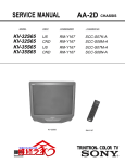
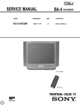
BA-4C CHASSIS
SERVICE MANUAL
MODEL
KV-24FV10
KV-24FV10
KV-25FV10
KV-25FV10C
COMMANDER
DEST
CHASSIS NO.
RM-Y168
US
SCC-S22A-A
RM-Y168
CND
SCC-S24A-A
RM-Y168
E
SCC-S23A-A
RM-Y168
E
SCC-S23C-A
KV-24FV10
RM-Y168
TRINITRON® COLOR TV
MICROFILM
KV-24FV10/25FV10/25FV10C
SPECIFICATIONS
KV-24FV10
KV-25FV10/10C
120V, 60 Hz
Auto Volt (120–220 VAC)
Video Input (1)
2
2
S Video Input (2)
1
1
Audio Input (3)
2
2
Audio Output (4)
1
1
10W x 2
10W x 2
150W
150W
1W
1W
(mm)
652 x 524.3 x 467.3 mm
652 x 524.3 x 467.3 mm
(in)
25 3/4 x 20 11/16 x 18 7/16 in
25 3/4 x 20 11/16 x 18 7/16 in
(kg)
40 kg
40 kg
(lbs)
88 lbs. 3 oz.
88 lbs. 3 oz.
Power Requirements
Number of inputs/outputs
Speaker Output (W)
Power Consumption (W)
In Use (Max)
In Standby
Dimensions (W/H/D)
Mass
1)
2)
3)
4)
1 Vp-p 75 ohms unbalanced, sync negative
Y: 1 Vp-p 75 ohms unbalanced, sync negative
C: 0.286 Vp-p (Burst signal), 75 ohms
500 mVrms (100% modulation), impedance: 47 kilohms
More than 408 mVrms at the maximum volume setting (variable)
More than 408 mVrms (fix)
Television system
American TV standard/NTSC
Channel coverage
VHF:2-13/UHF:14-69/CATV:1-125
Visible screen size
24" picture measured diagonally
Actual screen size
25" picture measured diagonally
Antenna
75 ohm external terminal for VHF/UHF
Supplied Accessories
Remote Commander RM-Y168 (all models)
Size AA (R6) batteries (2)
Optional Accessories
Dipole antenna
Connecting cables VMC-810S/820S, VMC-720M,
YC-15V/30V, RK74A
U/V mixer EAC-66
( • ) SRS (SOUND RETRIEVAL SYSTEM)
The ( • ) SRS (SOUND RETRIEVAL SYSTEM) is
manufactured by Sony Corporation under license
from SRS Labs, Inc. It is covered by U.S. Patent No.
4,748,669. Other U.S. and foreign patents pending.
The word ‘SRS’ and the SRS symbol ( • ) are
registered trademarks of SRS Labs, Inc.
Design and specifications are subject to change without notice.
—2—
BBE and BBE symbol are trademarks of BBE Sound,
Inc. and are licensed by BBE Sound, Inc. under U.S.
Patent No. 4,638,258 and 4,482,866.
KV-24FV10/25FV10/25FV10C
TABLE OF CONTENTS
Section
Title
Page
Warnings and Cautions ............................................................................................................................................................... 4
Self-Diagnostic Function ............................................................................................................................................................. 4
Safety Check Out Instructions ..................................................................................................................................................... 7
1.
2.
GENERAL ........................................................................................................................................................... 8
DISASSEMBLY
2-1.
2-2.
2-3.
2-4.
3.
SET-UP ADJUSTMENTS
3-1.
3-2.
3-3.
3-4.
3-5.
3-6.
4.
6-4.
Block Diagram ............................................................................................................................................................... 29
Circuit Board Location ................................................................................................................................................... 32
Printed Wiring Boards and Schematic Diagrams ......................................................................................................... 32
• A Board .................................................................................................................................................................... 33
• G Board .................................................................................................................................................................... 41
• V Board .................................................................................................................................................................... 45
• C Board .................................................................................................................................................................... 46
Semiconductors ............................................................................................................................................................ 51
EXPLODED VIEW
7-1.
8.
Setting the Service Adjustment Mode .......................................................................................................................... 22
Memory Write Confirmation Method ............................................................................................................................. 22
Adjustment Buttons and Indicators ............................................................................................................................... 22
A Board Adjustments .................................................................................................................................................... 25
DIAGRAMS
6-1.
6-2.
6-3.
7.
R582 and R584 Confirmation Method (HV Hold-Down Confirmation and Readjustments) ................................... 20
B+ Voltage Confirmation and Adjustment ..................................................................................................................... 20
CIRCUIT ADJUSTMENTS
5-1.
5-2.
5-3.
5-4.
6.
Beam Landing ............................................................................................................................................................... 16
Convergence ................................................................................................................................................................. 17
Focus ............................................................................................................................................................................. 18
Screen (G2) ................................................................................................................................................................... 18
Method of Setting the Service Adjustment Mode ......................................................................................................... 19
White Balance Adjustments .......................................................................................................................................... 19
SAFETY RELATED ADJUSTMENTS
4-1.
4-2.
5.
Rear Cover Removal ..................................................................................................................................................... 14
A Board Removal .......................................................................................................................................................... 14
Service Position ............................................................................................................................................................ 14
Picture Tube Removal ................................................................................................................................................... 15
Chassis .......................................................................................................................................................................... 52
ELECTRICAL PARTS LIST ................................................................................................................................................ 53
—3—
KV-24FV10/25FV10/25FV10C
WARNINGS AND CAUTIONS
CAUTION
ATTENTION
SHORT CIRCUIT THE ANODE OF THE PICTURE TUBE
AND THE ANODE CAP TO THE METAL CHASSIS, CRT
SHIELD, OR CARBON PAINTED ON THE CRT, AFTER
REMOVING THE ANODE.
APRES AVOIR DECONNECTE LE CAP DE L'ANODE, COURT-CIRCUITER
L'ANODE DU TUBE CATHODIQUE ET CELUI DE L'ANODE DU CAP AU
CHASSIS METALLIQUE DE L'APPAREIL, OU AU COUCHE DE CARBONE
PEINTE SUR LE TUBE CATHODIQUE OU AU BLINDAGE DU TUBE
CATHODIQUE.
WARNING!!
ATTENTION!!
AN ISOLATION TRANSFORMER SHOULD BE USED
DURING ANY SERVICE TO AVOID POSSIBLE SHOCK
HAZARD, BECAUSE OF LIVE CHASSIS. THE CHASSIS
OF THIS RECEIVER IS DIRECTLY CONNECTED TO THE
AC POWER LINE.
AFIN D'EVITER TOUT RESQUE D'ELECTROCUTION PROVENANT D'UN
CHÁSSIS SOUS TENSION, UN TRANSFORMATEUR D'ISOLEMENT DOIT
ETRE UTILISÉ LORS DE TOUT DÉPANNAGE. LE CHÁSSIS DE CE
RÉCEPTEUR EST DIRECTEMENT RACCORDÉ À L'ALIMENTATION SECTEUR.
SAFETY-RELATED COMPONENT WARNING!!
ATTENTION AUX COMPOSANTS RELATIFS A LA SECURITE!!
COMPONENTS IDENTIFIED BY SHADING AND MARK
ON THE SCHEMATIC DIAGRAMS, EXPLODED VIEWS,
AND IN THE PARTS LIST ARE CRITICAL FOR SAFE
OPERATION. REPLACE THESE COMPONENTS WITH
SONY PARTS WHOSE PART NUMBERS APPEAR AS
SHOWN IN THIS MANUAL OR IN SUPPLEMENTS
PUBLISHED BY SONY. CIRCUIT ADJUSTMENTS THAT
ARE CRITICAL FOR SAFE OPERATION ARE IDENTIFIED
IN THIS MANUAL. FOLLOW THESE PROCEDURES
WHENEVER CRITICAL COMPONENTS ARE REPLACED
OR IMPROPER OPERATION IS SUSPECTED.
LES COMPOSANTS IDENTIFIES PAR UNE TRAME ET PAR UNE MARQUE
SUR LES SCHEMAS DE PRINCIPE, LES VUES EXPLOSEES ET LES
LISTES DE PIECES SONT D'UNEIMPORTANCE CRITIQUE POUR LA
SECURITE DU FONCTIONNEMENT. NE LES REMPLACER QUE PAR DES
COMPOSANTS SONY DONT LE NUMERO DE PIECE EST INDIQUE DANS
LE PRESENT MANUEL OU DANS DES SUPPLEMENTS PUBLIES PAR SONY.
LES REGLAGES DE CIRCUIT DONT L'IMPORTANCE EST CRITIQUE POUR
LA SECURITE DU FONCTIONNEMENT SONT IDENTIFIES DANS LE
PRESENT MANUEL. SUIVRE CES PROCEDURES LORS DE CHAQUE
REMPLACEMENT DE COMPOSANTS CRITIQUES, OU LORSQU'UN
MAUVAIS FONTIONNEMENT SUSPECTE.
SELF-DIAGNOSTIC FUNCTION
The units in this manual contain a self-diagnostic function. If an error occurs, the STANDBY/TIMER LED will automatically begin to
flash. The number of times the LED flashes translates to a probable source of the problem. A definition of the STANDBY/TIMER LED
flash indicators is listed in the instruction manual for the user’s knowledge and reference. If an error symptom cannot be reproduced, the
Remote Commander can be used to review the failure occurrence data stored in memory to reveal past problems and how often these
problems occur.
Diagnostic Test Indicators
When an error occurs, the STANDBY/TIMER LED will flash a set number of times to indicate the possible cause of the problem. If
there is more than one error, the LED will identify the first of the problem areas.
Results for all of the following diagnostic items are displayed on screen. No error has occurred if the screen displays a “0”.
Diagnostic Item
Description
Power does not turn on
No. of Times
Self-diagnostic Display/
STANDBY/TIMER
Diagnostic Result
LED Flashes
Does not light
Probable Cause
Location
Detected Symptoms
• Power cord is not plugged in.
• Power does not come on.
• Fuse is burned out. (F600) (G Board)
• No power is supplied to the TV.
• AC power supply is faulty.
+B overcurrent (OCP)*
Vertical deflection stopped*
2 times
4 times
2:0 or 2:1
4:0 or 4:1
• H.OUT (Q502) is shorted. (A Board)
• Power does not come on.
• IC1751 is shorted. (C Board)
• Load on power line is shorted.
• +13V is not supplied. (A Board)
• Has entered standby state after horizontal raster.
• IC541 is faulty. (A Board)
• Vertical deflection pulse is stopped.
• Power line is shorted or power supply is stopped.
White balance failure
(not balanced)
5 times
5:0 or 5:1
• Video OUT (IC541) is faulty. (A Board)
• No raster is generated.
• IC301 is faulty. (A Board)
• CRT cathode current detection reference
pulse output is small.
• Screen (G2) is improperly adjusted.**
* If a +B overcurrent is detected, stoppage of the vertical deflection is detected simultaneously.
The symptom that is diagnosed first by the microcontroller is displayed on the screen.
** Refer to Screen (G2) Adjustments in Section 3-4 of this manual.
—4—
KV-24FV10/25FV10/25FV10C
Display of Standby/Timer LED Flash Count
2 times
4 times
5 times
LED ON 0.3 sec.
LED OFF 0.3 sec.
STANDBY/TIMER LED
LED OFF
3 sec.
Diagnostic Item
+B overcurrent
Vertical deflection stopped
White balance failure
Flash Count*
2 times
4 times
5 times
*One flash count is not used for self-diagnostic.
Stopping the Standby/Timer LED Flash
Turn off the power switch on the TV main unit or unplug the power cord from the outlet to stop the STANDBY/TIMER LAMP from
flashing.
Self-Diagnostic Screen Display
For errors with symptoms such as “power sometimes shuts off” or “screen sometimes goes out” that cannot be confirmed, it is
possible to bring up past occurrences of failure on the screen for confirmation.
To Bring Up Screen Test
In standby mode, press buttons on the Remote Commander sequentially, in rapid succession, as shown below:
Display
Channel 5
Sound volume
Power ON
Note that this differs from entering the service mode (sound volume + ).
Self Diagnostic Screen Display
SELF DIAGNOSTIC
2:
3:
4:
5:
101:
N/A
N/A
0
0
0
1
0
Numeral “0” means that no fault was detected.
Numeral “1” means a fault was detected one time only.
—5—
KV-24FV10/25FV10/25FV10C
Handling of Self-diagnostic Screen Display
Since the diagnostic results displayed on the screen are not automatically cleared, always check the self-diagnostic screen during
repairs. When you have completed the repairs, clear the result display to “0”.
Unless the result display is cleared to “0”, the self-diagnostic function will not be able to detect subsequent faults after completion
of the repairs.
Clearing the Result Display
To clear the result display to “0”, press buttons on the Remote Commander sequentially when the diagnostic screen is displayed,
as shown below:
Channel 8
ENTER
Quitting the Self-Diagnostic Screen
To quit the entire self-diagnostic screen, turn off the power switch on the Remote Commander or the main unit.
Self-diagnostic Circuit
IC301
Y/CHROMA JUNGLE
FROM
CRT
21 IK IN
FROM
IC521
PIN 7
18 HP/PROTECT
IC541
V. OUT
REF
IC001
SYSTEM
IO-BDAT 36
17 I-PROT
3
SDA 35
37 IO-SDAT
IC003
MEMORY
5
B-DAT
O-LED 18
DISPLAY
+B overcurrent (OCP)
Occurs when an overcurrent on the +B (115V) line is detected by pin 18 of IC301. If the voltage
of pin 18 of IC 301 is less than 1V when V.SYNC is more than seven verticals in a period, the unit
will automatically turn off.
Vertical deflection stopped
Occurs when an absence of the vertical deflection pulse is detected by pin 17 of IC001. Power
supply will shut down when waveform interval exceeds 2 seconds.
White balance failure
If the RGB levels* do not balance within 2 seconds after the power is turned on, this error will be
detected by IC301. TV will stay on, but there will be no picture.
*(Refers to the RGB levels of the AKB detection Ref pulse that detects 1K.)
—6—
KV-24FV10/25FV10/25FV10C
SAFETY CHECK-OUT
After correcting the original service problem, perform the
following safety checks before releasing the set to the
customer:
1. Check the area of your repair for unsoldered or poorly
soldered connections. Check the entire board surface
for solder splashes and bridges.
2. Check the interboard wiring to ensure that no wires
are “pinched” or touching high-wattage resistors.
3. Check that all control knobs, shields, covers, ground
straps, and mounting hardware have been replaced.
Be absolutely certain that you have replaced all the
insulators.
Leakage Test
The AC leakage from any exposed metal part to earth
ground and from all exposed metal parts to any exposed
metal part having a return to chassis, must not exceed
0.5 mA (500 microamperes). Leakage current can be
measured by any one of three methods.
1. A commercial leakage tester, such as the Simpson
229 or RCA WT-540A. Follow the manufacturers'
instructions to use these instructions.
2. A battery-operated AC milliammeter. The Data
Precision 245 digital multimeter is suitable for this job.
4. Look for unauthorized replacement parts, particularly
transistors, that were installed during a previous
repair. Point them out to the customer and
recommend their replacement.
5. Look for parts which, though functioning, show
obvious signs of deterioration. Point them out to the
customer and recommend their replacement.
6. Check the line cords for cracks and abrasion.
Recommend the replacement of any such line cord
to the customer.
3. Measuring the voltage drop across a resistor by
means of a VOM or battery-operated AC voltmeter.
The “limit” indication is 0.75 V, so analog meters must
have an accurate low voltage scale. The Simpson’s
250 and Sanwa SH-63Trd are examples of passive
VOMs that are suitable. Nearly all battery-operated
digital multimeters that have a 2 VAC range are
suitable (see Figure A).
How to Find a Good Earth Ground
7. Check the B+ and HV to see if they are specified
values. Make sure your instruments are accurate;
be suspicious of your HV meter if sets always have
low HV.
8. Check the antenna terminals, metal trim, “metallized”
knobs, screws, and all other exposed metal parts for
AC leakage. Check leakage as described below.
A cold-water pipe is a guaranteed earth ground; the coverplate retaining screw on most AC outlet boxes is also at
earth ground. If the retaining screw is to be used as your
earth ground, verify that it is at ground by measuring the
resistance between it and a cold-water pipe with an
ohmmeter. The reading should be zero ohms. If a cold-water
pipe is not accessible, connect a 60- to 100-watt troublelight (not a neon lamp) between the hot side of the
receptacle and the retaining screw. Try both slots, if
necessary, to locate the hot side on the line; the lamp
should light at normal brilliance if the screw is at ground
potential (see Figure B).
Figure A. Using an AC voltmeter to check AC leakage.
Figure B. Checking for earth ground.
—7—
The instructions mentioned here are partial abstracts from the Operating Instruction Manual.
The page numbers shown reflect those of the Operating Instruction Manual.
KV-24FV10/25FV10/25FV10C
SECTION 1
GENERAL
User Guide
Connecting Additional Equipment
Connecting Your TV
TV and VCR
TV
Read this chapter before setting up your TV for the first time. This section
covers basic connections in addition to any optional equipment you may
be connecting.
2
Basic Connections
VCR
TV with indoor or outdoor antenna, or CATV cable
Depending on the cable available in your home, choose one of the
connections below:
1
From
Cable/antenna
—8—
3 (Optional connection)
1
Connect the coaxial cable from your TV antenna or cable TV to the IN
jack on your VCR.
2
Connect a coaxial cable (not supplied) from the OUT jack on your
VCR to the VHF/UHF IN jack on the TV.
✍
To watch video programs from your VCR, tune your TV to channel 3 or 4 (as
set on the rear of your VCR).
(Optional connection)
3
✍
✍
If you are connecting to an indoor or outdoor antenna, it will be necessary to
adjust the orientation of the antenna for best reception.
3
4
If your VCR is equipped with video inputs, for better picture quality
you should connect A/V cables from AUDIO and VIDEO OUT on
your VCR to AUDIO/VIDEO IN on your TV. You can use the
button to switch between the TV and VCR inputs.
For optimum picture quality, use S VIDEO instead of the yellow A/V cable.
S VIDEO does not provide sound, the audio cables must still be connected.
Connecting Your TV
TV and Cable Box
User Guide
TV, VCR, and Cable box
TV
3
VCR
2
Cable box
—9—
1
Connect the coaxial cable from the wall to the IN jack on your cable
box.
2
Connect a coaxial cable (not supplied) from the OUT jack on your
cable box to the VHF/UHF IN jack on the TV.
✍
✍
1
4 (Optional connection)
Cable
To view channels from your cable box, tune your TV to channel 3 or 4 (as set
on the rear panel of your cable box).
If you will be controlling all channel selection through your cable box, you
should consider using the CHANNEL FIX feature on page 20.
1
Connect the coaxial cable from the wall to the IN jack on your cable
box.
2
Connect a coaxial cable (not supplied) from the OUT jack on your
cable box to the IN jack on your VCR.
3
Connect a coaxial cable (not supplied) from the OUT jack on your
VCR to the VHF/UHF IN jack on the TV.
✍
If you will be controlling all channel selection through your cable box, you
should consider using the CHANNEL FIX feature on page 20.
✍
5
6
For optimum picture quality, use S VIDEO instead of the yellow A/V cable.
S VIDEO does not provide sound, the audio cables must still be connected.
KV-24FV10/25FV10/25FV10C
(Optional connection)
4 If your VCR is equipped with video inputs, for better picture quality
you should connect A/V cables from AUDIO and VIDEO OUT on
your VCR to AUDIO/VIDEO IN on your TV. You can use the
button to switch between the TV and VCR inputs.
User Guide
TV, Digital Satellite Receiver and VCR
TV and Digital Satellite Receiver
TV
2
KV-24FV10/25FV10/25FV10C
Connecting Your TV
Satellite
antenna
From
cable/
antenna
1
TV
4
Cable
VCR
Satellite receiver
2
1
Satellite
antenna
cable
Satellite receiver
3
5
3
— 10 —
1
Connect the cable from your satellite antenna to SATELLITE IN on
the satellite receiver.
1
Connect the cable from your satellite antenna to SATELLITE IN on
the satellite receiver.
2
Attach the coaxial connector from your cable or antenna to
VHF/UHF IN on your VCR.
2
Attach the coaxial connector from your cable or antenna to
VHF/UHF on your TV.
3
Using a coaxial cable, connect VHF/UHF OUT on your VCR to
VHF/UHF on your TV.
3
Using A/V connectors, connect AUDIO and VIDEO OUT on your
satellite receiver to AUDIO and VIDEO IN on your TV.
4
Using A/V connectors, connect AUDIO and VIDEO OUT on your
satellite receiver to AUDIO and VIDEO IN on your VCR.
5
Using A/V connectors, connect AUDIO and VIDEO OUT on your
VCR to AUDIO and VIDEO IN on your TV.
✍
✍
You can use the
button to switch between the satellite receiver and TV.
✍
For optimum picture quality, use S VIDEO instead of the yellow A/V cable.
S VIDEO does not provide sound, your audio connectors must still be
connected.
7
8
To view from the satellite or VCR, select the video input to which your
satellite receiver or VCR is connected by pressing
on the remote
control.
Connecting Your TV
User Guide
Connecting a Camcorder
Connecting an audio system
Using A/V cables, connect AUDIO and VIDEO OUT on your camcorder
to AUDIO and VIDEO IN on your TV.
Using audio connectors, connect AUDIO OUT on your TV to one of the
unused line inputs (e.g. TV, AUX, TAPE 2) on your stereo.
(Front A/V Panel)
1
AUDIO-L
A/V output
AUDIO-R
Line
input
— 11 —
2
Connecting a DVD Player
✍
Using A/V connectors, connect LINE OUT on your DVD to VIDEO IN
on your TV.
Set your stereo to the chosen line input. See page 16 for additional audio
setup instructions.
(Rear of TV)
(Rear of DVD player)
A/V outputs
For optimum picture quality, use S VIDEO instead of the yellow A/V cable.
S VIDEO does not provide sound, your audio connectors must still be
connected.
9
10
KV-24FV10/25FV10/25FV10C
✍
Using the Remote Control and
Basic Functions
Cycles through available AUTO
VOLUME settings (see page 16).
This section shows you how to use more advanced buttons on the remote
control and how to use the on-screen menus.
Button
Description
POWER
Press when you want to turn
connected equipment on and off.
FUNCTION
Press when you want to control
connected equipment with your
remote control.
— 12 —
MUTING
Instantly turns off the sound.
Press again or press
to restore
sound.
SYSTEM OFF
Powers off all Sony equipment at
once.
TV/VIDEO
Cycles through available video
inputs.
Moves the cursor in the onscreen menus. Press the arrow
buttons to move the cursor, press
the center button to select or
access an option.
PICTURE MODE
Cycles through the available
VIDEO MODE settings.
SLEEP
Turns the TV off automatically in
approximately 30, 60 or 90
minutes. Cancel by pressing until
SLEEP OFF appears.
MTS/SAP
Cycles through the Multichannel TV Sound (MTS)
options: STEREO, SAP (Second
Audio Programming), MONO.
DISPLAY
Press once to show current time,
(if set) and channel number.
Press again to activate CAPTION
VISION settings, if available. To
cancel, press again until
DISPLAY OFF appears.
11
12
JUMP
Alternates back and forth
between the last two channels
-_ buttons.
selected with the
GUIDE
Brings up the custom guide of
your satellite receiver.
MENU
Displays the on-screen menu.
Press again to exit the menu at
any time.
RESET
Press to return to factory settings
while in the on-screen menu.
CODE SET
Use to program your remote
control to operate connected
video equipment, (see page 29).
KV-24FV10/25FV10/25FV10C
User Guide
User Guide
Other Information
Troubleshooting
If you are having a problem with your TV, try the suggestions below. If
the problem persists, contact your nearest Sony dealer.
❏
❏
❏
Make sure the power cord is plugged in.
If a red light is flashing on the front of your TV for
more than a few minutes, call your local service center.
Check your PARENTAL CONTROL settings, (pages
25-26).
Check the TV/VIDEO settings: when watching TV, set
to TV; when watching video equipment, set to VIDEO
(page 15).
Make sure the batteries have been inserted correctly
into the remote control.
Try another channel, it could be station trouble.
Poor or no
picture, good
sound
❏
❏
❏
Adjust PICTURE in the VIDEO menu (page 15).
Adjust BRIGHTNESS in the VIDEO menu (page 15).
Check the antenna and/or cable connections (page 3).
Good picture,
no sound
❏
Press
so that MUTING disappears from the
screen (page 11).
Check your AUDIO settings. Your TV may be set to
SAP (page 16).
No picture, no
sound
❏
❏
❏
— 13 —
❏
❏
Adjust COLOR in the VIDEO menu (page 15).
Only snow
appears on the
screen
❏
Check the CABLE setting in the SET UP menu
(page 20).
Check the antenna and/or cable connections (page 3).
Make sure the channel selected is currently
broadcasting.
Dotted lines or
stripes
❏
❏
Adjust the antenna.
Move the TV away from other electronic equipment.
Some electronic equipment can create electrical noise,
which can interfere with TV reception.
Double images
or ghosts
❏
Check your outdoor antenna or call your cable service.
Cannot receive
higher number
channels (UHF)
when using an
antenna
❏
Make sure CABLE is set to OFF in the SET UP menu
(page 20).
Use AUTO PROGRAM to add channels that are not
presently in the memory (page 20).
32
❏
❏
❏
❏
Remote
Control does
not operate
❏
❏
Batteries could be weak. Replace them (page 2).
Move the TV 3-4 feet away from fluorescent lights.
The TV needs
to be cleaned
❏
Clean the TV with a soft dry cloth. Never use strong
solvents such as thinner or benzine, which might
damage the finish of the cabinet.
Lost password
for PARENTAL
CONTROL
❏
In the password screen, enter the following master
password: 4357. After using the master password, you
must create a new password.
❏
Make sure CABLE is set to ON in the SET UP menu
(page 20).
Use AUTO PROGRAM to add channels that are not
presently in the memory (page 20).
If, after reading these operating instructions, you have additional questions related to the use of your
Sony television, please call our Direct Response Center at 1-800-222-SONY (7669) (U.S. residents
only). (416) 499-SONY (7669) (Canadian residents only).
33
KV-24FV10/25FV10/25FV10C
No color
Cable stations
don’t seem to
work
KV-24FV10/25FV10/25FV10C
SECTION 2
DISASSEMBLY
2-1. REAR COVER REMOVAL
Rear Cover
Seven Screws
(+BVTP 4x16)
Two Screws
(+BVTP 3x12)
2-2. A BOARD REMOVAL
2-3. SERVICE POSITION
C Board
V Board
G Board
V Board
A Board
A Board
G Board
— 14 —
C Board
KV-24FV10/25FV10/25FV10C
2-4. PICTURE TUBE REMOVAL
G Board
WARNING:
BEFORE REMOVING
THE ANODE CAP
A Board
Speaker
High voltage remains in the CRT even
after the power is disconnected. To
avoid electric shock, discharge CRT
before attempting to remove the anode
cap. Short between anode and CRT
coated earth ground strap.
Degaussing Coil
Tuner
Tension Spring (B)
C Board
Neck Assy.
Deflection Yoke
V Board
Tapping Screw
Coated
Earth
Ground
Strap
Anode Cap
Speaker
Picture Tube
Cushion
ANODE CAP REMOVAL
WARNING: High voltage remains in the CRT even after the power is disconnected. To avoid electrical shock, discharge the CRT before
attempting to remove the anode cap. Short between anode and coated earth ground strap of CRT.
NOTE:
After removing the anode, short circuit the anode of the picture tube and the anode cap to either the metal chassis, CRT shield,
or carbon painted on the CRT.
REMOVAL PROCEDURES
c
b
a
Anode Button
1
Turn up one side of the rubber cap in
the direction indicated by arrow a .
2
Use your thumb to pull the rubber
cap firmly in the direction indicated
by arrow b .
HOW TO HANDLE AN ANODE CAP
1
Do not use sharp objects which may cause damage to the
surface of the anode cap.
2
To avoid damaging the anode cap, do not squeeze the rubber
covering too hard. A material fitting called a shatter-hook terminal
is built into the rubber.
3
Do not force turn the foot of the rubber cover. This may cause
the shatter-hook terminal to protrude and damage the rubber.
— 15 —
3
When one side of the rubber cap
separates from the anode button,
the anode cap can be removed by
turning the rubber cap and pulling
it in the direction of arrow c .
KV-24FV10/25FV10/25FV10C
SECTION 3
SET-UP ADJUSTMENTS
The following adjustments should be made when
a complete realignment is required or when a new
picture tube is installed.
These adjustments should be performed with rated
power supply voltage unless otherwise noted.
Perform the adjustments in order as follows:
1. Beam Landing
2. Convergence
3. Focus
4. Screen (G2)
5. White Balance
Set the controls as follows unless otherwise noted.
Note: Test equipment required:
•
•
•
•
VIDEO MODE: STANDARD
PICTURE control: ............... Normal
BRIGHTNESS control ......... Normal
3-1. BEAM LANDING
Before beginning adjustment procedure:
Color bar pattern generator
Degausser
DC power supply
Digital multimeter
5. Move the deflection yoke forward and adjust so that the
entire screen becomes green.
1. Degauss the entire screen.
2. Feed in the white pattern signal.
Adjustment Procedure
1. Input a raster signal with the pattern generator.
2. Loosen the deflection yoke mounting screw and set the
purity control to the center as shown below.
Purity Control
6. Switch over the raster signal to red and blue and confirm
the condition.
7. When the position of the deflection yoke is determined,
tighten it with the deflection yoke mounting screw.
8. If landing at the corner is not right, adjust by using the disk
magnets.
3. Turn the raster signal of the pattern generator to green.
4. Move the deflection yoke backward and adjust the purity
control so that green is in the center and red and blue are
at the sides evenly.
Blue
Purity control
corrects this area
Red
a
b
c
d
Disk magnets
or rotatable disk
magnets correct
these areas (a-d)
Deflection yoke positioning
corrects these areas
Green
a
c
b
d
— 16 —
KV-24FV10/25FV10/25FV10C
3-2. CONVERGENCE
Horizontal Static Convergence
Before starting convergence adjustments:
If the blue dot does not converge with the red and green dots,
perform the following:
1. Perform FOCUS, V.LIN AND V.SIZE adjustments.
1. Move BMC magnet (a) to correct insufficient H. Static
convergence.
2. Set BRIGHTNESS control to minimum.
3. Feed in dot pattern.
2. Rotate BMC magnet (b) to correct insufficient V. Static
convergence.
Vertical Static Convergence
1. Adjust V.STAT magnet to converge red, green and blue
dots in the center of the screen. (Vertical movement adjust
V.STAT RV to converge.)
3. After adjusting the BMC magnet, repeat Beam Landing
Adjustment.
PURITY
V. STAT
Center dot
R
G
B
BMC MAGNET
V.STAT magnet
R G B
RV1750
V.STAT
BMC magnet
a
2. Tilt the V.STAT magnet and adjust static convergence to
open or close the V.STAT magnet.
b
Dynamic Convergence Adjustment
When the V.STAT magnet is moved in the direction of arrows
a and b, red, green, and blue dots move as shown below:
Before performing this adjustment, perform Horizontal
and Vertical Static Convergence Adjustment.
1. Slightly loosen deflection yoke screw.
(1)
2. Remove deflection yoke spacers.
a
b
a
b
b
B
B
G
G
R
R
3. Move the deflection yoke for best convergence,
as shown below:
(2)
a
R
R B G R B
G
G
B R G B R
G B
R G B
B G R
b
B
G R
B R G B R
G
G
R B G R B
(3)
b
a
B
R
G
G
b
B
R
4. Tighten the deflection yoke screw.
5. Install the deflection yoke spacers.
— 17 —
B G R R G B
KV-24FV10/25FV10/25FV10C
TLH Plate Adjustment
3-3. FOCUS
•
•
Input crosshatch pattern
1. Adjust FOCUS control for best picture.
•
Adjust the Horizontal Convergence of red and blue dots
by tilting the TLH plate on the deflection yoke.
Adjust PICTURE QUALITY to standard, PICTURE and
BRIGHTNESS to 50%, and OTHER to standard.
(TLV)
YCH
Focus (FV)
TLH Plate
TLV
Screen (G2)
RV1750
V.STAT
XCV
3-4. SCREEN (G2)
C Board
1. Input a dots pattern.
V Board
2. Set the PICTURE and BRIGHTNESS controls at minimum
and COLOR control at normal.
3. Adjust SBRT, GCUT, BCUT in service mode with an
oscilloscope as shown below so that voltages on the red,
green, and blue cathodes are 170 VDC.
BR
(R)(B)
RB
(B)(R)
TLH+
TLH-
170 VDC
Pedestal
Ground
1. Adjust XCV core to balance X axis.
2. Adjust YCH VR to balance Y axis.
4. Observe the screen and adjust SCREEN (G2) VR in FBT
to obtain the faintly visible background of dot signal.
3. Adjust vertical red and blue convergence with V.TILT
(TLV VR.)
Perform adjustments while tracking items 1 and 2.
Screen-Corner Convergence
1. Affix a permalloy assembly corresponding to the
misconverged areas.
a
b
a
b
a-d: screen-corner
misconvergence
c
c
d
d
— 18 —
KV-24FV10/25FV10/25FV10C
3-6. WHITE BALANCE ADJUSTMENTS
3-5. METHOD OF SETTING THE SERVICE
ADJUSTMENT MODE
1. Input an entire white signal with burst.
2. Set to Service Adjustment Mode.
Service Mode Procedure
3. Set DCOL to “0”.
1. Standby mode (power off).
4. Set the PICTURE and BRIGHTNESS to minimum.
2. Display
Sound volume +
Channel 5
Power
on the Remote Commander (press each button within a
second).
5. Adjust with SBRT if necessary.
6. Select GCUT and BCUT with
7. Adjust with
and
and
.
for the best white balance.
8. Set PICTURE and BRIGHTNESS to maximum.
Service Adjustment Mode In
9. Select GDRV and BDRV with
1. The CRT displays the item being adjusted.
10. Adjust with
Disp.
(Item)
SERVICE
or
on the Remote Commander to select the
3. Press
data.
or
on the Remote Commander to change the
then
to save into the memory.
Service Adjustment Mode Memory
Turn set off then on to exit service adjustment mode.
SERVICE
WRITE
for the best white balance.
12. To write into memory, press
0
2. Press
item.
4. Press
.
11. Reset DCOL to “1”.
Item
Data
HSIZ
and
and
MUTING
Green
ENTER
Red
— 19 —
then
.
KV-24FV10/25FV10/25FV10C
SECTION 4
SAFETY RELATED ADJUSTMENTS
4-1.
R582 AND R584 CONFIRMATION
METHOD (HV HOLD-DOWN
CONFIRMATION) AND
READJUSTMENTS
Hold-down Readjustment
If the setting indicated in step 2 of Hold-down Operation
Confirmation cannot be met, readjustment should be performed
by altering the resistance value of R582 and/or R584
components marked with .
The following adjustments should always be performed when
replacing the following components which are marked with
on the schematic diagram:
A BOARD:
T505
FBT
DY, CRT, C507, C520, C573, C574, C575,
D572, D573, D574, IC521, IC301, R578,
R579, R582, R583, R584, R585, R586,
R587, T504, T505
ammeter
3.0 mA DC
range
ABL
+
A
-
IABL
Preparation Before Confirmation
1. Using a Variac, apply AC input voltage: 120 ± 2 VAC
(or 120-220 ± 2 VAC for KV-25FV10/10C only.)
4-2. B+ VOLTAGE CONFIRMATION AND
ADJUSTMENT
2. Turn the POWER switch ON.
Note: The following adjustments should always be performed
when replacing the following components, which are marked
with on the schematic diagram on the G Board.
3. Input a white signal and set the PICTURE and
BRIGHTNESS controls to maximum.
4. Confirm that the voltage between C574 (+) or TP503
and ground is more than 105 VDC.
G BOARD:
Hold-down Operation Confirmation
IC601, PH600
1. Using a Variac, apply AC input voltage: 130 ± 2 VAC
(or 120-220 ± 2 VAC for KV-25FV10/10C only.)
1. Connect the current meter between Pin 11 of the FBT
(T505) and the PWB land where Pin 11 would normally
attach. (See Figure 1 on the next page.)
2. Input a dot signal.
3. Set the PICTURE and BRIGHTNESS controls to minimum.
2. Input a dot signal and set PICTURE and BRIGHTNESS
to minimum: IABL = 100 ± 100 mA.
4. Confirm that the voltage of A Board TP-600 is 135 ± 3 VAC.
5. If step 3 is not satisfied, replace the components listed
above, then repeat steps 1–3.
3. Confirm the voltage of A Board TP-600 is 135 ± 3 VDC.
4. Connect the digital voltmeter and the DC power supply
via diode 1SS119 to C574 (+) and ground. (See Figure 1
on the next page.)
5. Increase the DC power voltage gradually until the picture
blanks out.
6. Turn DC power source off immediately.
7. Read the digital voltmeter indication
(standard: 138.0 ± .3 VDC).
8. Input a white signal and set PICTURE and BRIGHTNESS
to maximum: IABL = 1650 ± 100 mA.
9. Repeat steps 4 to 7.
— 20 —
KV-24FV10/25FV10/25FV10C
DIGITAL
MULTIMETER
+
–
TP600
ABL11
T505
FBT
R582
R584
C574
AMMETER
3mA dc range
POWER
SUPPLY
DIGITAL
MULTIMETER
1SS119
A
+
–
+
–
Figure 1
— 21 —
+
–
KV-24FV10/25FV10/25FV10C
SECTION 5
CIRCUIT ADJUSTMENTS
ELECTRICAL ADJUSTMENTS BY REMOTE COMMANDER
Use the Remote Commander (RM-Y168) to perform the circuit adjustments in this section.
NOTE: Test Equipment Required:
•
•
•
•
Pattern generator
Frequency counter
Digital multimeter
Audio oscillator
5-1. Setting the Service Adjustment Mode
5-2. Memory Write Confirmation Method
1. Standby mode (power off).
1. After adjustment, remove the power plug from the AC
outlet, then plug it in again.
2. Display
Sound volume +
Channel 5
Power
2. Turn the power switch ON and set to service mode.
on the Remote Commander (press each button within a
second).
3. Call the adjusted items again to confirm they were adjusted.
5-3. Adjustment Buttons and Indicators
Service Adjustment Mode On
1. The CRT displays the item being adjusted.
Disp.
(Item)
SERVICE
Item
Data
HSIZ
0
MUTING
POWER
MUTING
VTR/DVD SAT/CABLE
POWER
TV
—— FUNCTION ——
SYSTEM
OFF
VTR/DVD SAT/CABLE TV
TV/VTR
2. Press
item.
or
on the Remote Commander to select an
3. Press
or
on the Remote Commander to change the data.
4. Press
then
PICTURE
MODE
SLEEP MTS/SAP DISPLAY
3
to save into the memory.
DISPLAY
Service Adjustment Mode Memory
1
2
3
4
5
6
7
8
5
6
1
SERVICE
WRITE
MUTING
Green
4
JUMP
1. Press
then
initialize.
SERVICE
ENTER
0
8
ENTER
9
ENTER
Red
TV/SAT
GUIDE
RESET
MENU
on the Remote Commander to
RESET
VOLUME
Carry out step 1 when adjusting
IDs 0–4 and when replacing
and adjusting IC003.
VOL
CH
+
–
+
–
CODE SET
2. Turn set off then on to exit service adjustment mode.
RM-Y168
— 22 —
KV-24FV10/25FV10/25FV10C
Adjustment Items
INITIAL DATA
NO.
ITEM
1
2
3
4
5
6
7
8
9
10
11
12
13
14
15
16
17
18
19
20
21
22
23
24
25
26
27
28
29
30
31
32
33
34
35
36
37
38
39
40
41
42
43
44
45
46
47
48
49
50
51
52
53
54
55
56
57
58
59
60
61
62
HSIZ
HPOS
VBOW
VANG
TRAP
PAMP
UPIN
LPIN
BLK0
VMLV
AGN2
REFP
VBLK
JPSW
VSIZ
VPOS
VLIN
SCOR
VZOM
EHT
ASP
SCRL
HBLK
LBLK
RBLK
VUSN
HDW
EWDC
LVLN
UVLN
RDRV
GDRV
BDRV
RCUT
GCUT
BCUT
DCOL
SHUE
SCOL
SBRT
RON
GON
BON
AXPL
AXNT
CBPF
CTRP
COFF
KOFF
SSHP
SHPF
PREL
Y-DC
GAMM
ABLM
VTH
YDEL
NCOL
FSC
K-ID
HOSC
VSS
FUNCTION
HORIZONTAL SIZE ADJ.
HORIZONTAL POS. ADJ.
VRT LINE BOWING ADJ.
VRT LINE BOW SLANT ADJ.
HORIZ. TRAPEZOID ADJ.
HORIZ. PIN DISTORTION ADJ.
UPPER PIN DISTORTION ADJ.
LOWER PIN DISTORTION ADJ.
VERTICAL BLANKING ON/OFF
VELOCITY MODULATION LEVEL
AGING 2
REFERENCE PULSE POSITION
VERTICAL BLANKING ON/OFF
VERTICAL SIZE ADJ.
VERTICAL POSITION ADJ.
VERTICAL LINEARITY ADJ.
VERTICAL “S” CORRECTION ADJ.
16:9 CRT Z MODE ON/OFF
VRT HI-VOLT. CORRECTION
ASPECT RATIO CONTROL
16:9 CRT Z MODE TRANS SCROLL
HORIZONTAL BLANKING ON/OFF
LEFT BLANKING ADJ.
RIGHT BLANKING ADJ.
V SAW WAVEFORM COMPRESS
H. DRIVE PULSE WIDTH
“PARABOLA” EW/DC ADJ.
LOWER SCREEN BTM VRT LIN ADJ.
UPPER SCREEN BTM VRT LIN ADJ.
R OUTPUT DRIVE CONTROL
G OUTPUT DRIVE CONTROL
B OUTPUT DRIVE CONTROL
R OUTPUT CUTOFF CONTROL
G OUTPUT CUTOFF CONTROL
B OUTPUT CUTOFF CONTROL
DYNAMIC COLOR ON/OFF
SUB HUE
SUB COLOR
SUB BRIGHTNESS
R OUTPUT ON/OFF
G OUTPUT ON/OFF
B OUTPUT ON/OFF
AXIS PAL
AXIS NTSC
CHROMA BPF ON/OFF
Y TRAP FILTER ON/OFF
COLOR ON/OFF
SET COLOR KILLER
SUB SHARPNESS
SHARPNESS CIRCUIT F0
PRE/OVR SHOOT SWITCHING
DC TRANS RATIO SWITCHING
GAMMA CORRECTION AMNT
ABL MODE SWITCHING
ABL CD VHT SWITCHING
Y DELAY TIME CONTROL
NO COLOR ID
FSC OUT ON/OFF
KILLER ID CONTROL SW
H VCO OSCILLATION FREQ
V SYNC SLICE LEVEL
DATA
RANGE
0-63
0-63
0-15
0-15
0-15
0-63
0-63
0-63
0, 1
0-3
0, 1
0, 1
0, 1
0, 1
0-63
0-63
0-15
0-15
0, 1
0-15
0-63
0-63
0, 1
0-15
0-15
0, 1
0, 1
0, 1
0-15
0-15
0-63
0-63
0-63
0-15
0-15
0-15
0, 1
0-31
0-31
0-31
0, 1
0, 1
0, 1
0, 1
0, 1
0, 1
0, 1
0, 1
0, 1
0-15
0, 1
0, 1
0, 1
0-3
0, 1
0, 1
0-15
0, 1
0, 1
0, 1
0-15
0, 1
— 23 —
NTSC
PALM/
PALN
35
33
5
7
7
7
36
36
35
33
5
7
7
7
36
36
VIDEO
0
Palette mode controls this register
0
0
0
0
47
47
32
32
6
8
0
6
47
31
1
12
5
0
1
0
0
0
31
25
25
10
7
6
0
14
14
14
15
1
1
1
0
0
0
1
0
0
6
1
1
1
1
Palette mode controls this register
1
1
7
1
1
0
7
1
AVERAGE
DATA
38
21
9
5
7
32
39
39
0
2
0
0
0
0
49
32
6
8
0
6
47
31
1
12
5
0
1
0
0
0
36
26
25
8
6
7
1
15
15
15
1
1
1
0
0
1
1
0
0
7
1
1
1
1
1
1
7
1
1
0
7
0
KV-24FV10/25FV10/25FV10C
INITIAL DATA
NO.
ITEM
63
64
65
66
67
68
69
70
71
72
73
74
75
76
77
78
79
80
81
82
83
84
85
86
87
88
89
90
91
92
93
94
95
HSS
HMSK
VTMS
CDMD
AFC
FIFR
SBAL
SBAS
STRE
BBEL
BBEH
SRND
BBE
DISP
TROT
HCLW
HCHG
ABL0
ABL1
SYSC
VENH
CBPC
BYCF
KILC
LDOT
CORE
ID0
ID1
ID2
ID3
ID4
ID5
ID6
FUNCTION
H SYNC SLICE LEVEL
SELECT SIGNAL VTIM PIN
V CNT DWN MODE SWITCHING
AFC LOOP GAIN SWITCHING
FIELD FREQUENCY
SUB BALANCE
SUB BASS
SUB TREBLE
BBE LOW
BBE HIGH
SURROUND
BBE ON/OFF
O.S.D DISPLAY POSITION
TILT CORRECTION
HORIZONTAL COUNT LOWER LIMIT
HORIZONTAL COUNT HIGH LIMIT
COLOR SYSTEM
VERTICAL ENHANCEMENT
DATA
RANGE
0, 1
0, 1
0-3
0-3
0-3
0-3
0-15
0-15
0-15
0-15
0-15
0-63
0, 1
0-63
0-63
0-127
0-127
0, 1
0-7
0-7
0-7
0, 1
0, 1
0, 1
0, 1
0, 1
0-255
0-255
0-255
0-255
0-255
0-255
0-255
PALM/
PALN
NTSC
0
0
0
0
0
3
VIDEO
AVERAGE
DATA
3
0
1
7
9
9
12
9
13
1
22
31
16
64
16
64
0
0
6
Palette mode controls this register
0
0
0
0
0
201
19
173
43
251
0
64
0
0
0
0
0
3
7
9
9
12
9
13
1
15
31
16
64
1
7
6
4
0
0
0
0
0
See ID Map
See ID Map
See ID Map
See ID Map
See ID Map
See ID Map
See ID Map
Notes:
No. 1–95 show the order that each adjustment mode may be selected while in service mode.
Data Range shows the range of possible settings for each adjustment mode.
Initial Data shows the standard settings for each adjustment mode.
— 24 —
SERVICE
ID0
25
KV-24FV10/25FV10/25FV10C
Feature ID Map
MODEL
DEST. ID-0
8. Adjust the value of RDRV with
1.85 ± 0.05 Vp-p.
ID-1
ID-2
ID-3
ID-4
ID-5
ID-6
KV-24FV10
US
217
19
173
11
219
0
64
KV-24FV10
CND
217
19
173
43
219
0
64
KV-25FV10
E
145
19
173
83
251
0
64
KV-25FV10C
E
145
19
173
83
251
0
64
and
for
White
1.85 ± 0.05 Vp-p
Black
5-4. A BOARD ADJUSTMENTS
9. Reset the item DCOL to 1.
10. Reset GON and BON values to 1.
H. Frequency (Free Run) Check
R ON:
G ON:
B ON:
1. Input a TV mode (RF) with no signal.
2. Connect a frequency counter to base of Q501
(TP-500 H. DRIVE).
ON
ON
ON
(1)
(1)
(1)
11. Reset Picture, Color, and Bright to normal values:
3. Check H. Frequency for 15735 ± 200 Hz.
PICTURE:
COLOR:
BRIGHT:
V. Frequency (Free Run) Check
12. Press
1. Select video 1 with no signal input.
MAX
CENTER
CENTER
then
to save into the memory.
2. Set the conditions for a standard setting.
Display Position Adjustment (DISP)
3. Connect the frequency counter on the A board to TP-508
(V OUT) or CN 501 pin
(V DY+) and ground.
1. Input a color-bar signal.
2. Set to Service Adjustment Mode.
4. Check that V. Frequency shows 60 ± 4 Hz.
3. Select DISP with
Sub Contrast Adjustment (RDRV)
and
.
4. Adjust values of DISP with
to the center.
1. Input a color-bar signal and set the level to 75%.
2. In Standard mode, set PICTURE to maximum, COLOR to
minimum, and BRIGHTNESS to center.
and
to adjust characters
5. Write to memory by pressing
then
.
6. Check to see if the text is displayed on the screen.
3. Activate the Service Adjustment Mode.
SERVICE
4. Set both GON and BON items. Using
and ;
set each to the following values. Leave RON set to 1.
SERVICE
RON
DISP
15
1
1: ON
0: OFF
Sub Bright Adjustment (SBRT)
1. Input a monoscope signal.
R ON:
G ON:
B ON:
ON (1)
OFF (0)
OFF (0)
2. Activate the Service Adjustment Mode.
3. Set the PICTURE and BRIGHTNESS to minimum.
5. Select the item DCOL item and set it to 0.
4. Select the SBRT item with
6. Connect an oscilloscope probe to C board, CN1752 pin
TP47R (RED OUT).
5. Adjust the values of SBRT with
faintly visible crosshatch.
7. Select RDRV with
6. Press
and
.
— 25 —
then
and
.
and
to obtain a
to save into the memory.
KV-24FV10/25FV10/25FV10C
Sub Hue, Sub Color Adjustment (SHUE, SCOL)
H. Center Adjustment (HPOS)
1. Input a color-bar signal.
2. Activate the Service Adjustment Mode.
Perform this adjustment after performing H. Frequency
(Free Run) check.
3. Select the DCOL item and set the value to 0.
1. Input a crosshatch signal.
4. Connect an oscilloscope probe to C Board, CN1752
Pin
or TP47b (BLUE OUT).
2. Activate the Service Adjustment Mode.
5. Select the SHUE and SCOL item with
4. Adjust the value of HPOS with
horizontal center.
and
3. Select the HPOS item with
.
6. While showing the SHUE item, adjust the waveform with
and
until the second and third bars show the same
level (V2 = V3 ± 0.15 Vp-p).
5. Press
and
then
.
and
for the best
to save into the memory.
7. While showing the SCOL item, adjust the waveform with
and
until the first and fourth bars show the same
level (V1 = V4 ± 0.15 Vp-p).
V1
V2
V4
V3
H.Size Adjustment (HSIZ)
1. Input a monoscope signal.
2. Activate the Service Adjustment Mode.
3. Select HSIZ with
4. Adjust with
8. Select the DCOL item and reset to 1.
9. Press
then
5. Press
to save into the memory.
and
and
.
for the best Horizontal size.
then
to save into the memory.
V. Size Adjustment (VSIZ)
1. Input a crosshatch signal.
2. Activate the Service Adjustment Mode.
3. Select the VSIZ item with
4. Adjust value of VPOS with
center.
5. Press
then
and
and
.
for the best vertical
V. Linearity (VLIN), V Correction (VSCO),
Pin Amp (PAMP) and Horizontal Trapezoid
(TRAP) Adjustments
1. Input a crosshatch signal.
to save into the memory.
2. Activate the Service Adjustment Mode.
3. Select VLIN, VSCO, PAMP, and PPHA with with
4. Adjust with
5. Press
and
for the best Horizontal size.
then
to save into the memory.
V LINEARITY (VLIN)
V. Center Adjustment (VPOS)
Perform this adjustment after performing H. Frequency
(Free Run) check.
V CORRECTION (VSCO)
1. Input a crosshatch signal.
2. Activate the Service Adjustment Mode.
3. Select the VPOS item with
and
.
4. Adjust value of VPOS with
center.
and
for the best vertical
5. Press
then
PIN AMP (PAMP)
to save into the memory.
HORIZONTAL TRAPEZOID (TRAP)
— 26 —
and
.
KV-24FV10/25FV10/25FV10C
V Angle (VANG), V Bow (VBOW), Upper pin
(UPIN) and Low Pin (LPIN) Adjustments
1. Input a crosshatch signal.
2. Activate the Service Adjustment Mode.
3. Select VANG, VBOW, UPIN, and LPIN with
4. Adjust with
5. Press
and
and
.
for the best picture.
then
to save into the memory.
V ANGLE (VANG)
V BOW (VBOW)
UPPER PIN (UPIN)
LOW PIN (LPIN)
Service Adjustment Mode Memory
1. Change the value of the DCOL item to 1.
2. After completing all adjustments, press
then
.
Read From Memory
SERVICE
READ
Green
0
Red
ENTER
— 27 —
KV-24FV10/25FV10/25FV10C
NOTES:
— 28 —
KV-24FV10/25FV10/25FV10C
NOTES:
KV-24FV10/25FV10/25FV10C
NOTES:
KV-24FV10/25FV10/25FV10C
SECTION 6
DIAGRAMS
6.2 CIRCUIT BOARD LOCATIONS
6.1 BLOCK DIAGRAM
• When replacing parts shown in the table below, be sure to
perform the related adjustments.
Part Replaced (
)
DY, CRT, C507, C520, C573, C574,
C575, D572, D573, D574, IC521,
IC301, R578, R579, R582, R583,
R584, R585, R586, R587, T504,
T505..................................A Board
Adjustment (
)
HV HOLD-DOWN
(R582, R584)
V Board
IC601, PH600...................G Board
C Board
B+ VOLTAGE
CONFIRMATION
• All voltages are in Volts
• Voltage is DC with respect to ground unless otherwise
noted.
• Readings are taken with a 10MΩ digital multimeter.
A Board
• Readings are taken with a color-bar signal input.
G Board
6-3. PRINTED WIRING BOARDS AND
SCHEMATIC DIAGRAMS
• All capacitors are in µF unless otherwise noted.
pF: µµF 50 WV or less are not indicated except for
electrolytic and tantalums.
• All electrolytics are 50V unless otherwise specified.
• Voltage variations may be noted due to normal production
tolerance.
• Circled numbers are waveform references.
• *
: cannot be measured
•
: B + Line
•
-----
•
RESISTOR
• All resistors are in ohms.
MΩ = 1000KΩ
•
: nonflammable resistor
•
: fusible resistor
•
: internal component
•
: panel designation and adjustment for repair
•
: earth-ground
•
: earth-chassis
• All variable and adjustable resistors have characteristic
curve B, unless otherwise noted.
• The components identified by
in this manual have been
carefully factory-selected for each set in order to satisfy
regulations regarding X-ray radiation. Should replacement
be required, replace only with the value originally used.
• When replacing components identified by , make the
necessary adjustments indicated. If results do not meet
the specified value, change the component identified
by
and repeat the adjustment until the specified value
is achieved (refer to Safety Related Adjustments on
page 20).
— 29 —
853 1 A Block Diagram.p65
1
— 30 —
— 31 —
3/3/99, 9:55 AM
: Signal path
Reference Information
• Indication of resistance, which does not have one for
rating electrical power, is as follows:
Pitch: 5mm
Rating electrical power 1/4W (CHIP: 1/10W)
KΩ = 1000Ω
: B − Line
COIL
CAPACITOR
:
:
:
:
:
:
:
:
:
:
:
:
:
:
:
:
:
:
RN
RC
FPRD
FUSE
RW
RS
RB
LF-8L
TA
PS
PP
PT
MPS
MPP
ALB
ALT
ALR
METAL FILM
SOLID
NON FLAMMABLE CARBON
NON FLAMMABLE FUSIBLE
NON FLAMMABLE WIREWOUND
NON FLAMMABLE METAL OXIDE
NON FLAMMABLE CEMENT
ADJUSTMENT RESISTOR
MICRO INDUCTOR
TANTALUM
STYROL
POLYPROPYLENE
MYLAR
METALIZED POLYESTER
METALIZED POLYPROPYLENE
BIPOLAR
HIGH TEMPERATURE
HIGH RIPPLE
Note:
The components identified by shading and
mark
are critical for safety. Replace only with the part
number specified.
The symbol
(displayed on component side of the
circuit board) indicates fast operating fuse. Replace
only with fuse of the same rating as marked.
Les composants identifiés per un tramé et une marque
sont critiques pour la sécurité. Ne les remplacer que
par une piéce portant le numéro spécifié.
Le symbole
indique une fusible a action rapide.
Doit etre remplacee par une fusible de meme yaleur,
comme marque.
— 32 —
KV-24FV10/25FV10/25FV10C
A BOARD SCHEMATIC DIAGRAM (TOP)
A BOARD WAVEFORMS
1
A BOARD IC VOLTAGE LIST
2
1.1V p-p (V)
5
3
2.1V p-p (V)
6
1.1V p-p (V)
9
7
10
13
5.9V p-p (V)
17
21
25
20
23
26
738mV p-p
24
55.9V p-p
27
53.8V p-p (V)
3.0V p-p (V)
1.4V p-p (V)
201.6V p-p (V)
29.5V p-p (V)
16
19
22
1.4V p-p (V)
2.9V p-p (V)
1.6V p-p (V)
2.8V p-p (V)
12
15
18
2.1V p-p (V)
1.5V p-p (V)
5.4V p-p (V)
3.1V p-p (V)
8
11
14
3.5V p-p (H)
869mV p-p (V)
2V p-p (V)
838mV p-p
4
4.7V p-p (V)
712mV p-p (V)
IC001
1231V p-p (V)
28
30.5V p-p (V)
29
214.1V p-p
54.1V p-p (V)
PIN
1
2
3
4
5
6
7
8
9
10
11
12
13
14
15
16
17
18
19
20
21
22
23
24
25
26
27
28
29
30
31
32
33
34
35
36
37
38
39
40
41
42
43
44
45
46
47
48
49
50
51
52
VOLT
1.0
4.8
0
.3
4.9
0
0
0
0
0
0
4.9
0
5.0
4.9
0
−0.4
4.9
5.0
1.8
0.2
2.2
0
2.4
2.4
0
4.9
0
0
5.0
5.0
.1
5.0
2.4
5.0
5.0
5.0
5.0
5.0
0
0
.1
5.0
.1
0
0
0
0
0
0
0
0
IC002
PIN
1
2
3
4
5
6
7
8
VOLT
7.4
0
5.4
0
0
5.0
0
5.0
IC003
PIN
1
2
3
4
5
6
7
8
VOLT
0
0
0
0
4.9
4.9
0
5.0
IC004
PIN
1
2
3
VOLT
4.9
5.0
0
IC010
PIN
1
2
3
4
5
6
7
8
VOLT
3.0
4.9
2.9
0
0
5.0
2.2
0
IC202
PIN
1
2
3
4
5
6
7
8
VOLT
7.1
7.1
7.1
0
7.1
7.1
7.1
14.3
IC203
PIN
1
2
3
4
5
6
7
VOLT
4.9
4.2
4.9
4.2
4.9
6.1
4.9
8
9
10
11
12
13
14
15
16
17
18
19
20
21
22
23
24
25
26
27
28
29
30
31
32
33
34
35
36
37
38
39
40
41
42
1
4.2
4.9
4.2
4.9
0
4.9
4.2
0
4.2
0
0
5.0
5.0
0
4.2
5.3
4.2
4.2
4.2
4.9
0
4.9
0
4.9
4.2
4.2
5.3
0
4.3
3.6
9.0
3.5
4.2
5.4
4.2
IC301
PIN
1
2
3
4
5
6
7
8
9
10
11
12
13
14
15
16
17
VOLT
3.4
5.2
1.6
5.2
4.9
4.4
3.3
5.0
5.2
0
4.0
2.4
3.6
3.5
5.5
7.6
.7
18
19
20
21
22
23
24
25
26
27
28
29
30
31
32
33
34
35
36
37
38
39
40
41
42
43
44
45
46
47
48
1.1
3.1
2.6
1.8
1.4
1.5
1.7
.1
4.3
4.6
4.6
0
4.6
4.6
4.6
8.9
5.0
5.0
0
4.6
5.3
5.3
0
5.2
7.5
5.2
9.0
5.4
4.7
1.8
.1
IC302
PIN
1
2
3
4
5
6
7
8
9
10
11
12
13
14
15
16
17
18
19
20
21
VOLT
3.6
0
2.4
5.1
1.5
1.4
0
5.0
5.0
0
0
0
0
0
5.1
0
0
5.2
2.5
1.9
2.5
22
23
24
25
26
27
28
3.6
4.1
1.7
4.0
3.1
5.2
0
IC402
PIN
1
2
3
4
5
6
7
8
9
10
11
12
13
14
15
16
17
18
19
20
21
22
23
24
25
26
27
28
29
30
31
32
VOLT
0
0
0
4.7
4.5
4.5
4.5
4.5
4.5
4.5
4.5
4.5
0
2.0
9.0
9.0
0
4.9
2.0
0
4.5
4.5
4.5
4.5
4.5
4.5
4.5
4.5
4.5
4.5
3.7
4.5
IC404
PIN
1
2
3
4
5
6
7
8
9
10
11
VOLT
7.1
0
14.2
7.1
3.7
0
4.0
4.0
6.9
4.0
4.0
12
13
14
15
16
17
4.0
.1
7.1
14.2
0
7.1
2
3
4
5
6
7
8
9
10
11
12
13
14
15
16
A
IC405
PIN
1
2
3
4
5
6
7
8
9
10
VOLT
9.0
4.5
4.5
4.5
4.3
0
0
4.3
4.5
4.5
IC521
PIN
1
2
3
4
5
6
7
8
VOLT
.1
3.5
2.4
0
9.3
10.2
0
13.1
B
C
D
IC541
PIN
1
2
3
4
5
6
7
VOLT
1.8
13.1
−13.6
0
.3
13.2
1.8
E
IC603
PIN
I
O
G
4
VOLT
12.8
9.0
0
12.8
F
All voltages are in V
G
H
A Board (Top)
— 33 —
853 2 A Schematic Top.p65
1
— 34 —
— 35 —
3/5/99, 11:54 AM
— 36 —
17
18
19
KV-24FV10/25FV10/25FV10C
A BOARD SCHEMATIC DIAGRAM (BOTTOM)
1
2
3
4
5
6
7
8
9
10
11
12
13
14
15
16
17
18
19
[TUNING CONTROL, Y/C/J, DEFLECTION, TUNER/IF, AUDIO, MTS]
H
1
2
3
4
5
6
7
8
A
I
B
J
A BOARD TRANSISTOR
VOLTAGE LIST
Q001
Q002
Q081
Q101
Q200
Q201
Q203
Q204
Q286
Q287
Q288
Q300
Q302
Q305
Q306
Q307
Q308
Q309
Q310
Q350
Q351
Q352
Q353
Q354
Q355
Q356
Q357
Q358
Q359
Q360
Q390
Q401
Q501
Q502
Q521
Q522
Q555
Q571
Q604
Q650
Q870
K
L
M
N
A BOARD LOCATION LIST
DIODE
A BOARD MARK (*) LIST
REF NO.
R540
LOC.
J-17
KV-24FV10/25FV10
2.2K
KV-25FV10C
JW (10MM)
D001
D002
D003
D004
D005
D006
D007
D008
D009
D010
D205
D207
D208
E-4
H-10
H-8
H-8
H-11
B-11
D-10
B-10
G-10
G-9
H-2
F-2
C-9
D250
D251
D252
D253
D254
D255
D302
D501
D502
D503
D504
D520
D521
D522
G-2
G-2
G-3
G-2
G-2
H-1
G-8
A-5
C-5
C-5
B-5
C-6
D-5
E-4
D523
D541
D552
D561
D562
D571
D504
D572
D573
D574
D581
D650
D800
D871
E-4
E-3
C-4
D-3
D-3
B-1
B-5
E-2
E-2
E-2
E-3
G-6
B-7
F-8
IC
IC001
IC002
IC003
IC004
IC010
IC202
IC203
IC301
IC302
IC402
IC404
IC405
IC521
G-9
H-10
H-9
D-11
F-9
E-2
F-3
G-7
G-5
E-9
B-9
E-10
E-3
IC541
IC603
D-3
D-9
TRANSISTOR
Q001
Q002
Q081
Q082
Q101
Q200
Q201
Q203
Q204
Q286
Q287
G-9
H-4
F-8
F-8
H-3
E-1
E-1
D-9
E-7
G-4
G-3
Q288
Q300
Q301
Q302
Q305
Q306
Q307
Q308
Q309
Q310
Q350
Q351
Q352
Q354
G-4
F-8
E-8
F-4
F-4
F-8
F-8
F-8
F-7
F-8
F-5
F-6
F-6
F-7
Q555
Q571
Q604
Q650
Q870
F-7
C-2
F-6
G-6
G-8
B
5.2
4.52
.4
0
.7
.7
5.6
0
4.5
5.3
7.4
.6
4.4
3.2
1.6
1.5
1.4
3.6
3.6
3.9
2.4
8.1
2.7
4.1
2.4
8.1
2.7
3.5
3.2
4.7
5.0
.6
-.8
-.2
.1
.1
2.0
134.7
.1
5.8
.3
C
.7
8.97
0
7.2
0
0
0
.1
0
0
9.0
.7
9.0
0
0
0
0
1.8
0
0
8.1
2.6
0
0
8.1
2.7
0
8.9
0
0
9.0
0
97.7
135.6
3.4
21.1
9.0
10.7
4.1
9.0
3.9
E
4.9
3.89
.9
0
0
0
.1
0
5.2
5.9
6.8
0
3.8
3.8
2.3
2.1
2.0
3.7
3.7
4.6
1.8
8.7
3.3
4.7
1.8
8.7
3.3
2.9
3.8
5.3
4.3
0
0
0
0
0
2.2
134.5
0
5.2
0
C
D
E
F
G
H
NOTE:
Portions of the circuit marked as shown are high
voltage areas. Use care to prevent electric shocks
during inspection or repair.
All voltages are in V
— 37 —
853 3 A Schematic Bottom.p65
1
— 38 —
— 39 —
3/5/99, 11:59 AM
— 40 —
9
10
11
KV-24FV10/25FV10/25FV10C
G BOARD SCHEMATIC DIAGRAM
1
2
3
4
5
6
7
8
9
10
11
12
13
14
G BOARD LOCATION LIST
15
DIODE
D601
D602
D603
D604
D605
D606
D607
D608
D609
D610
D611
D612
D613
A
NOTE:
Portions of the circuit marked as shown are high
voltage areas. Use care to prevent electric shocks
during inspection or repair.
B
[POWER SUPPLY]
1
2
3
4
5
6
7
8
E-2
C-2
A-4
A-5
C-4
B-4
A-5
A-4
C-7
B-6
B-7
D-1
A-7
D614
D615
D617
D618
D619
D620
D630
D631
D632
D633
D634
D635
D637
D638
A-7
C-8
B-9
D-5
D-5
E-1
A-9
D-3
D-4
D-6
D-5
D-5
D-4
D-5
G BOARD
IC VOLTAGE LIST
IC
IC601
IC602
B-6
D-7
TRANSISTOR
Q601
Q602
Q603
Q605
Q606
Q607
Q610
Q644
A-4
A-5
A-7
D-5
D-4
D-1
D-1
D-1
Q601
Q602
Q603
Q606
Q607
Q610
Q644
IC602
PIN
1
2
3
VOLT
134.9
123.1
0
Q605
B
−58.1
−57.6
−40.8
.5
.7
0
0
G
1.8
C
−58.2
−40.8
−54.9
.8
.1
.7
13.6
D
154.3
E
−58.5
−58.0
−40.8
.1
0
0
0
S
.1
All voltages are in V
9
G BOARD MARK (*) LIST
REF NO.
C600
C607
C613
C616
C617
C636
C637
C663
D609
F600
IC601
JW632
JW633
JW634
JW635
JW636
JW637
JW638
JW639
R600
R601
R633
R634
R637
R646
R672
R674
T601
T602
T603
THP601
VDR600
A
D
B
E
C
F
D
G
E
H
I
853 4 G Board Schematic.p65
VOLT
−56.3
−58.0
101.4
−41.0
−58.1
All voltages are in V
C
A Board (Bottom)
IC601
PIN
1
2
3
4
5
G BOARD TRANSISTOR
VOLTAGE LIST
G Board
1
— 41 —
— 43 —
— 42 —
3/5/99, 12:06 PM
— 44 —
LOC.
F-2
E-4
E-7
C-8
D-8
E-11
E-11
D-2
D-8
G-2
D-9
E-4
F-4
E-4
D-4
D-3
D-3
D-2
D-2
F-5
F-4
E-7
E-7
D-8
E-7
E-8
E-7
E-4
F-3
D-11
D-3
G-2
KV-24FV10
0.47 125V
0.47 125V
680 250V
#
#
.0047 250V
.0047 250V
.22 125V
#
6.3A 125V
STR-F6626
#
#
#
#
7.5MM
7.5MM
#
#
#
4.7M
390K
JW 5MM
#
15MM
15MM
15K
1-426-717-11
1-431-838-11
1-433-806-11
1-809-539-11
1-803-585-11
KV-25FV10/10C
0.47 300V
0.47 300V
560 400V
0.022 400V
220p 1KV
#
#
.22 300V
RU-1P
6.3A 250V
STR-F6656
10MM
10MM
10MM
10MM
#
#
5MM
5MM
8.2M
#
270K
270K
100K
5.6K
5.6K
5.6K
#
1-426-717-11
1-433-807-11
1-803-540-11
1-803-587-11
#: Not mounted
KV-24FV10/25FV10/25FV10C
V BOARD SCHEMATIC DIAGRAM
1
2
3
4
5
6
7
8
9
C BOARD SCHEMATIC DIAGRAM
[CRT DRIVE, RGB DRIVE]
10
1
2
3
1
4
2
3
4
5
6
A
A
A
B
B
B
C BOARD
IC VOLTAGE LIST
IC1707
PIN
1
2
3
4
5
6
7
8
C
C
C
D
D
E
E
D
VOLT
3.8
4.5
4.5
0
6.1
6.1
6.1
9.0
IC1751
PIN
1
2
3
4
5
6
7
8
9
E
VOLT
2.3
2.2
2.1
0
3.7
205.0
145.0
141.0
132.0
All voltages are in V
[VELOCITY MODULATION]
1
2
V BOARD TRANSISTOR
VOLTAGE LIST
3
4
5
Q961
Q962
Q963
Q965
Q967
Q968
A
F
C BOARD WAVEFORMS
B
2.4
2.4
134.4
.7
6.2
5.5
C
9.0
5.5
83.7
83.7
9.0
0
E
1.8
1.8
134.8
.1
5.9
5.9
1
2
3
G
132.8V p-p (H)
135.9V p-p (H)
140.6V p-p (H)
All voltages are in V
NOTE:
Portions of the circuit marked as shown are high
voltage areas. Use care to prevent electric shocks
during inspection or repair.
B
C
V
— 45 —
853 5 CV Boards.p65
1
— 46 —
— 47 —
3/5/99, 12:10 PM
C Boards
KV-24FV10/25FV10/25FV10C
A BOARD IC BLOCK DIAGRAMS
A BOARD IC541 TDA8172
8
1
IN1
V+
7
60
k
OUT2
+
-
6
4
Inv. Input 1
4
Power
Amplifier
+
Non-Inv. Input 7
OUT 2 -
5
IN 3
IN2
10
+
-
IN 4
MUTE
STANDBY
A BOARD: IC402 BH3868FS
5
1
Y CLAMP
APED
VM OUT/
V PROT
EB-Y IN
ER-Y IN
EY IN
YUV SW
R1 IN
G1 IN
B1 IN
YS1
R2 IN (YOUT)
G2 IN (R-YOUT)
B2 IN (B-YOUT)
YS2/YM
31
30
29
EYUV CLAMP
YUV SW
<YSEL>
YUVOUT
<YUVOUT>
C VCO
CHROMA
AMP
ACC DET.
COLOR AMP
<COLOR>
<C OFF>
AXIS
<AXIS NTSC>
<AXIS PAL>
COLOR KILLER
<<KILLER ID OFF>>
BUFFER
+
V/l
OA
14
CLAMP
DC TRAN
<DC TRAN>
FILTER ALIGNMENT
CAL. by fsc
BPF
<C BPF>
Y/C MIX
RGB CLAMP
12
60
k
11
+
-
+
-
V/l
OA
17
OUT 4 +
45 k
13
5
INTERFACE
DIAGNOSTIC
6
16
15
12
OUT2
TRE2
BAS2
43
C1 IN
2
CVBS2/Y2 IN
A BOARD: IC203 MM1313AD
DIAG
CVBS1/Y1 IN
Vcc
38
16
MTV-V 41
V1-V
1
V2-V
7
6dB
34 V OUT1
6dB
3
V2-Y
9
V1-C
5
37 Y OUT1
6dB
29 C IN1
0dB
0dB
V2-C 11
-6dB
Y SW
ATT
7
MONITOR SW
COMB-Y IN
9
VIDEO SW
MON OUT
6
<VIDEO SEL>
<S SEL>
V SYNC SEP
<VSS>
COUNTDOWN
<CD MODE>
<INTERLACE>
LINE COUNTER
V TIM GEN.
<JUMP SW>
<REF P>
<VBLKW>
VSAW GEN
VTIM
H SYNC SEP
<HSS>
<H MASK>
AFC
<AFC GAIN>
<FH HIGH>
<<HLOCK>>
<<HCENT>>
HSAW GEN.
<HOSC>
(ZAP)
9
8
7
BBASB2
BBASA2
5
BTREA2
6
BTREB2
IN2
SOUT
V1-L
2
V2-L
8
4
10
12
16
33
3
LS2
2
LS1
33 L OUT1
-6dB
32 R OUT1
-6dB
24 R OUT2
26
6 S1
BIAS
12 S2
SCL 19
21 ADDRESS
2
SDA 20
I C LOGIC
28 MUTE
GND
GND
— 49 —
— 50 —
3/3/99, 2:02 PM
REG
19
39 C OUT1
V3-R 16
STV-R
IREF
<HD W>
18
6dB
V2-R 10
HD GEN.
5
22 L OUT2
40
EW PARABOLA FUNC.
<H SIZE>
<TRAPEZIUM>
<PIN AMP>
<EW DC>
<UPPER CPIN>
<LOWER CPIN>
17
V3-L 14
V1-R
<S CORRECTION>
<V LINEARITY>
<EHT COMP>
20
STV-L 25
MTV-R
VD SAW FUNC.
<VON>
<V SIZE>
<V POSITION>
<ASPECT>
<SCROLL>
<UPPER VLIN>
<LOWER VLIN>
<V ZOOM>
<JUMP SW>
PHASE DET.
<H POSITION>
<AFC BOW>
<AFC ANGLE>
HPROT
<<HNG>>
H TIM GEN.
<H BLK>
<LEFT HBLK>
<RIGHT HBLK>
I2C BUS
DECODER
STATUS I/F
DAC
SW
WIDE SAW FUNC.
Y
4
COMB-C IN
TRAP + EQ
<TRAP OFF>
AKB
<<IKR>>
23 V OUT2
31 Y IN1
V1-Y
41
CHROMA SW
MTV-L 42
4
BBE
VOL
TV/C2 IN
SHARPNESS DL
SHARPNESS AMP
<SHARPNESS>
<SHP F0>
<PRE/OVER>
ABL/PEAK LIM
<ABL MODE>
<ABL VTH>
CLAMP
RGB 1/2
VPROT
<<VGN>>
VM AMP
<VM LEV>
(OFF YS/YM)
ACC AMP
OUT 3 -
42
ABL FIL
3
ABL IN
21
IK IN
24
B OUT
23
G OUT
22
R OUT
35
SDA
34
SCL
14
VD-
13
VD+
11
EW
DEMOD.
DPIC
<DPIC>
<AGING>
<AGING2>
Gnd
30
853 6 A Pinouts.p65
32
THERMAL
PROTECTION
BIAS 36
BH3868FS
— 48 —
25
APC
<HUE>
VC2
11
13
TC
10
TONE VOL
R-S
PHAS LPF
SHFT AMP
L-R
L+R
AGC
VOL
VCC
14
VCC
LOGIC
CONTROL
VRE
TONE VOL
L+S
BBE
CHIP
1
FILTER
26
Output
V3-V 13
BIAS
17
18
19
20
21
22
23
24
25
26
27
28
31
29
30
AGCADJ
32
PS1
27
VCC1
PS2
28
REG
IN1
36
1 REF
BBASA1
37
GND1
BBASB1
38
HD
BTREA1
39
HP/PROTECT
BTREB1
15
V TIM
BAS1
1
SCP
TRE1
8
AFC FIL
OUT1
40
FSC
<FSC SW>
STV-V 27
VC1
44
4
PGND1 PGND2
BC
46
45 k
2
SDR
47
CHROMA
IN 5
SCL
45
TDA8172
9
45
k
IN2
GND2
Flyback
Generator
BUFFER
60
k
V-
3
FLYBACK
GENERATOR
OUT 1 +
OA
45
k
-
3
6
1
45 k
Vpx
BUFFER
IN1
+
-
V/l
30 k
+
2
45 k
OA
+
V/l
8
Vpx
Output
State Supply
Vcc2
+
-
TDA8580Q/N1
+
2
Supply
Voltage
7
60
k
IN 2
-
15
YS1 SW
<RGB SEL>
YM SW
YS2 SW
DYNAMIC COLOR
<DYNAMIC C>
PICTURE AMP
<PICTURE>
GAMMA AMP
<GAMMA>
CLAMP
BRIGHT CONT
<BRIGHT>
DRIVE AMP
<R/G/B DRIVE>
CUTOFF CONT.
<R/G/B CUTOFF>
R/G/B BLK
<PON>
<R/G/B ON>
OUT1
3
FSCOUT
IN 1
VP2
Xtal
A BOARD: IC202 UPC4558M
VP1
A BOARD: IC301 CXA2131S
APC FIL
A BOARD: IC404 TDA8580Q/N1
KV-24FV10/25FV10/25FV10C
6-4. SEMICONDUCTORS
2SC5426-01
2SB709A
2SD601A
2SC3209LK-TP
2SA1309A
2SC3311A
2SD2144S
LETTER SIDE
C
B
E
E
C
B
E
C
B
E
2SA1091O-TPE2
2SD1292
2SA1837
2SC4159-E
C
2SK2845
G
D
B
C
E
E
S
C
B
1SS83TD
D1NL2OU-TA
EL1Z-V1
ERA22-08TP3
GP08DPKG23
RGP02-17PKG23
RGP10GPKG3
RGP10GPKG23
RGP15GPKG23
ERC04-06S
ERC06-15S
MTZJ-T-77-2.2A
MTZJ-T-77-5.1C
MTZJ-T-775.6C
MTZJ-T-77-7.5A
MTZJ-T-77-8.2B
MTZJ-T-77-10B
MTZJ-T-7730D
RU-1P
1SS133T-77
D1N2OR-TA
D1NS4-TA
MTZJ-T-7712C
MTZJ-T-77-20B
MTZJ-T-77-33B
MTZJ-T-77-39
RD3.3ES-T1B
CATHODE
RU4AM-T3
CATHODE
CATHODE
ANODE
ANODE
ANODE
DAP202K-T-146
RD9.1EW-T1
D4SB60L-F
D5LC20U
CATHODE
MARKING SIDE VIEW
3
2
1
3
ANODE
2
ANODE
1
CATHODE
— 51 —
B
KV-24FV10/25FV10/25FV10C
SECTION 7
EXPLODED VIEW
•
Items with no part number and no
description are not stocked because
they are seldom required for routine
service.
Note:
• The component parts of an
assembly are indicated by the
reference numbers in the remarks
column.
Note:
The components identified by
are critical for
shading and mark
safety. Replace only with par t
number specified.
•
Items marked “ * ” are not stocked
since they are seldom required for
routine service. Some delay should be
anticipated when ordering these items.
Les composants identifies per un
sont critiques
trame et une marque
pour la securite. Ne les remplacer
que par une piece portant le numero
specifie.
24
7-1. CHASSIS
4-041-268-01 SCREW (7) TAPPING
7-685-663-79 SCREW +BVTP 4X16 TYPE2 TT (B)
7-685-661-91 SCREW +BVTP 4X12 TYPE2 TT (B)
7-685-647-79 SCREW +BVTP 3X10 TYPE2 TT (B)
31
20
32
9
21
18
7
22
10
23
8
17
16
19
29
15
3
4
5
1
14
13
27
30
28
12
29
2
11
6
REF. NO. PART NO.
DESCRIPTION
REMARK
1
2
3
4
5
X-4036-358-1
4-046-160-01
4-068-307-01
4-068-308-01
4-068-309-01
BEZNET ASSY
EMBLEM (NO. 9), SONY
BUTTON, MULTI
GUIDE, LED
BUTTON, FUNCTION
6
7
8
9
10
4-068-306-01
4-057-714-01
8-453-011-21
3-704-372-31
1-452-896-11
DOOR
PIECE ASSY, TLH CORRECTION
NECK ASSY (NA299-S)
HOLDER, HV CABLE
COIL, NA ROTATION (RT200)
11
12
13
14
15
8-733-250-05
4-053-005-01
1-451-475-11
* A-1342-465-A
* A-1331-898-A
16
17
4-036-329-01 SPRING (B), TENSION
1-419-104-11 COIL, ALUMINIUM DEMAGNETIZATION
(ALL EXCEPT KV-24FV10)
1-416-925-11 COIL, ALUMINIUM DEGAUSSING
(KV-24FV10 ONLY)
* A-1311-737-A G (VAR) MOUNTED PC BOARD
(KV-24FV10 ONLY)
2-6
REF. NO. PART NO.
18
19
19
20
20
20
21
17
18
CRT (25RSN/A60LPN70X)
SPACER, DY
DEFLECTION YOKE (Y25RSA)
V MOUNTED PC BOARD
C MOUNTED PC BOARD
REMARK
* A-1311-754-A G (VAR) MOUNTED PC BOARD
(ALL EXCEPT KV-24FV10)
* A-1298-795-A A COMPLETE PC BOARD (24FV10 ONLY)
* A-1298-920-A A COMPLETE PC BOARD (ALL EXCEPT 24FV10)
1-790-315-21 CORD, AC POWER (WITH CONNECTOR) 10A125V
(KV-24FV10 ONLY)
1-751-057-21 CORD, POWER (WITH CONNECTOR) 10A/125V
(KV-25FV10 ONLY)
1-769-796-71 CORD, POWER (WITH CONNECTOR) 10A/125V
(KV-25FV10C ONLY)
1-453-306-11 FBT, NX4011//X4J4
22
23
24
27
1-766-374-11
8-598-431-00
4-068-303-01
* 4-068-305-01
28
29
30
31
32
1-529-334-11
4-374-745-31
1-529-333-11
4-062-047-01
1-452-032-00
— 52 —
DESCRIPTION
PLUG, F-PIN
TUNER, FSS BTF-WA411
COVER, REAR
BOX, SPEAKER
SPEAKER (13X8CM)
CUSHION (A)
4CM TWEETER
PIECE A (110), CONV CORRECT
MAGNET, DISC
KV-24FV10/25FV10/25FV10C
SECTION 8
ELECTRICAL PARTS LIST
Note:
The components identified by
shading and mark
are critical for
safety. Replace only with par t
number specified.
• The components identified by
in this
manual have been carefully factoryselected for each set in order to satisfy
regulations regarding X-ray radiation.
Should replacement be required, replace
only with the value originally used.
•
Note:
Les composants identifies per un
trame et une marque
sont critiques
pour la securite. Ne les remplacer
que par une piece portant le numero
specifie.
REF. NO. PART NO.
RESISTORS
• All resistors are in ohms
• F : nonflammable
CAPACITORS
• MF = µF
Items marked “ * ” are not stocked
since they are seldom required for routine
service. Some delay should be anticipated
when ordering these items.
• All variable and adjustable resistors have
characteristic curve B, unless otherwise
noted.
DESCRIPTION
REMARK
* A-1298-920-A A COMPLETE PC BOARD
(KV-25FV10C ONLY)
* A-1298-795-A A COMPLETE PC BOARD
(ALL EXCEPT KV-25FV10C)
4-382-854-11 SCREW (M3X10), P, SW (+)
4-070-495-01 HEAT SINK, AUDIO FD (IC404)
CAPACITOR
INDUCTORS
• UH = µH, MMH = mH
When indicating parts by reference
number, please include the board name.
REF. NO. PART NO.
DESCRIPTION
REMARK
C060
C062
C065
C070
C076
C080
1-163-005-11
1-164-161-11
1-163-009-11
1-163-259-91
1-163-009-11
1-126-964-11
CERAMIC CHIP
CERAMIC CHIP
CERAMIC CHIP
CERAMIC CHIP
CERAMIC CHIP
ELECT
470PF
0.0022MF
0.001MF
220PF
0.001MF
10MF
10%
10%
10%
5%
10%
20%
50V
50V
50V
50V
50V
50V
C081
C091
C092
C101
C102
1-126-964-11
1-163-231-11
1-163-231-11
1-126-963-11
1-126-933-11
ELECT
CERAMIC CHIP
CERAMIC CHIP
ELECT
ELECT
10MF
15PF
15PF
4.7MF
100MF
20%
5%
5%
20%
20%
50V
50V
50V
50V
16V
C001
C002
C003
C004
C005
1-163-259-91
1-126-960-11
1-126-960-11
1-106-343-00
1-126-960-11
CERAMIC CHIP
ELECT
ELECT
MYLAR
ELECT
220PF
1MF
1MF
0.001MF
1MF
5%
20%
20%
10%
20%
50V
50V
50V
200V
50V
C150
C151
C207
C208
C209
1-126-941-11
1-104-664-11
1-126-959-11
1-126-959-11
1-126-963-11
ELECT
ELECT
ELECT
ELECT
ELECT
470MF
47MF
0.47MF
0.47MF
4.7MF
20%
20%
20%
20%
20%
25V
25V
50V
50V
50V
C006
C007
C008
C009
C011
1-163-035-00
1-163-259-91
1-163-009-11
1-104-664-11
1-163-009-11
CERAMIC CHIP
CERAMIC CHIP
CERAMIC CHIP
ELECT
CERAMIC CHIP
0.047MF
220PF
0.001MF
47MF
0.001MF
5%
10%
20%
10%
50V
50V
50V
25V
50V
C211
C212
C213
C222
C223
1-126-964-11
1-126-963-11
1-126-964-11
1-126-964-11
1-104-664-11
ELECT
ELECT
ELECT
ELECT
ELECT
10MF
4.7MF
10MF
10MF
47MF
20%
20%
20%
20%
20%
50V
50V
50V
50V
25V
C012
C014
C017
C019
C020
1-163-009-11
1-164-004-11
1-126-960-11
1-163-135-00
1-130-495-00
CERAMIC CHIP
CERAMIC CHIP
ELECT
CERAMIC CHIP
FILM
0.001MF
0.1MF
1MF
560PF
0.1MF
10%
10%
20%
5%
5%
50V
25V
50V
50V
50V
C225
C226
C255
C256
C257
1-163-017-00
1-126-963-11
1-104-760-11
1-126-960-11
1-126-960-11
CERAMIC CHIP
ELECT
CERAMIC CHIP
ELECT
ELECT
0.0047MF
4.7MF
0.047MF
1MF
1MF
10%
20%
10%
20%
20%
50V
50V
50V
50V
50V
C021
C028
C030
C034
C035
1-163-259-91
1-163-005-11
1-163-259-91
1-163-037-11
1-163-017-00
CERAMIC CHIP
CERAMIC CHIP
CERAMIC CHIP
CERAMIC CHIP
CERAMIC CHIP
220PF
470PF
220PF
0.022MF
0.0047MF
5%
10%
5%
10%
10%
50V
50V
50V
50V
50V
C258
C259
C284
C285
C287
1-126-959-11
1-163-021-91
1-104-664-11
1-126-933-11
1-126-959-11
ELECT
CERAMIC CHIP
ELECT
ELECT
ELECT
0.47MF
0.01MF
47MF
100MF
0.47MF
20%
10%
20%
20%
20%
50V
50V
25V
16V
50V
C036
C037
C038
C039
C045
1-163-009-11
1-164-161-11
1-126-941-11
1-126-964-11
1-164-161-11
CERAMIC CHIP
CERAMIC CHIP
ELECT
ELECT
CERAMIC CHIP
0.001MF
0.0022MF
470MF
10MF
0.0022MF
10%
10%
20%
20%
10%
50V
50V
25V
50V
50V
C288
C289
C290
C301
C303
1-126-960-11
1-126-960-11
1-164-005-11
1-163-233-11
1-126-963-11
ELECT
ELECT
CERAMIC CHIP
CERAMIC CHIP
ELECT
1MF
1MF
0.47MF
18PF
4.7MF
20% 50V
20% 50V
25V
5% 50V
20% 50V
C046
C047
C048
1-104-664-11 ELECT
1-163-259-91 CERAMIC CHIP
1-163-009-11 CERAMIC CHIP
47MF
20% 25V
220PF 5% 50V
0.001MF 10% 50V
C304
C305
C306
1-163-038-91 CERAMIC CHIP
1-164-004-11 CERAMIC CHIP
1-164-004-11 CERAMIC CHIP
0.1MF
0.1MF
0.1MF
25V
10% 25V
10% 25V
— 53 —
KV-24FV10/25FV10/25FV10C
Note:
Note:
The components identified by
shading and mark
are critical for
safety. Replace only with part
number specified.
REF. NO. PART NO.
DESCRIPTION
REMARK
C307
C308
C309
C310
C311
1-126-964-11
1-126-964-11
1-163-021-91
1-126-960-11
1-163-021-91
ELECT
ELECT
CERAMIC CHIP
ELECT
CERAMIC CHIP
10MF
10MF
0.01MF
1MF
0.01MF
20%
20%
10%
20%
10%
C312
C313
C314
C316
C317
1-126-767-11
1-163-021-91
1-163-231-11
1-163-021-91
1-163-021-91
ELECT
CERAMIC CHIP
CERAMIC CHIP
CERAMIC CHIP
CERAMIC CHIP
1000MF
0.01MF
15PF
0.01MF
0.01MF
C318
C319
C320
C321
C324
1-163-021-91
1-126-963-11
1-126-959-11
1-163-133-00
1-163-243-11
CERAMIC CHIP
ELECT
ELECT
CERAMIC CHIP
CERAMIC CHIP
C330
C332
C334
C350
C351
1-163-003-11
1-163-251-11
1-126-933-11
1-163-021-91
1-163-021-91
C352
C353
C354
C355
C356
Les composants identifies per un
trame et une marque
sont critiques
pour la securite. Ne les remplacer
que par une piece portant le numero
specifie.
REF. NO. PART NO.
DESCRIPTION
50V
50V
50V
50V
50V
C398
C399
C400
C401
C402
1-163-021-91
1-126-964-11
1-126-963-11
1-126-963-11
1-126-963-11
CERAMIC CHIP
ELECT
ELECT
ELECT
ELECT
0.01MF
10MF
4.7MF
4.7MF
4.7MF
20%
10%
5%
10%
10%
16V
50V
50V
50V
50V
C403
C404
C405
C406
C407
1-163-009-11
1-163-034-00
1-164-182-11
1-163-034-00
1-165-319-11
CERAMIC CHIP
CERAMIC CHIP
CERAMIC CHIP
CERAMIC CHIP
CERAMIC CHIP
0.001MF 10% 50V
0.033MF
50V
0.0033MF 10% 50V
0.033MF
50V
0.1MF
50V
0.01MF
4.7MF
0.47MF
470PF
47PF
10%
20%
20%
5%
5%
50V
50V
50V
50V
50V
C410
C411
C412
C413
C414
1-165-319-11
1-126-933-11
1-126-960-11
1-126-960-11
1-163-017-00
CERAMIC CHIP
ELECT
ELECT
ELECT
CERAMIC CHIP
0.1MF
100MF
1MF
1MF
0.0047MF
20%
20%
20%
10%
50V
16V
50V
50V
50V
CERAMIC CHIP
CERAMIC CHIP
ELECT
CERAMIC CHIP
CERAMIC CHIP
330PF
100PF
100MF
0.01MF
0.01MF
10%
5%
20%
10%
10%
50V
50V
16V
50V
50V
C415
C416
C417
C418
C419
1-163-034-00
1-126-963-11
1-126-933-11
1-126-964-11
1-126-961-11
CERAMIC CHIP
ELECT
ELECT
ELECT
ELECT
0.033MF
4.7MF
100MF
10MF
2.2MF
20%
20%
20%
20%
50V
50V
16V
50V
50V
1-126-964-11
1-163-021-91
1-163-021-91
1-126-933-11
1-163-021-91
ELECT
CERAMIC CHIP
CERAMIC CHIP
ELECT
CERAMIC CHIP
10MF
0.01MF
0.01MF
100MF
0.01MF
20%
10%
10%
20%
10%
50V
50V
50V
16V
50V
C420
C422
C425
C427
C428
1-126-960-11
1-126-943-11
1-126-943-11
1-126-961-11
1-136-169-00
ELECT
ELECT
ELECT
ELECT
FILM
1MF
2200MF
2200MF
2.2MF
0.22MF
20%
20%
20%
20%
5%
50V
25V
25V
50V
50V
C357
C358
C359
C360
C361
1-163-021-91
1-126-964-11
1-126-964-11
1-163-021-91
1-163-123-00
CERAMIC CHIP
ELECT
ELECT
CERAMIC CHIP
CERAMIC CHIP
0.01MF
10MF
10MF
0.01MF
180PF
10%
20%
20%
10%
5%
50V
50V
50V
50V
50V
C430
C431
C432
C433
C434
1-164-182-11
1-163-034-00
1-163-009-11
1-126-963-11
1-126-963-11
CERAMIC CHIP
CERAMIC CHIP
CERAMIC CHIP
ELECT
ELECT
0.0033MF
0.033MF
0.001MF
4.7MF
4.7MF
10% 50V
50V
10% 50V
20% 50V
20% 50V
C362
C364
C365
C366
C367
1-126-960-11
1-163-021-91
1-163-021-91
1-163-021-91
1-163-021-91
ELECT
CERAMIC CHIP
CERAMIC CHIP
CERAMIC CHIP
CERAMIC CHIP
1MF
0.01MF
0.01MF
0.01MF
0.01MF
20%
10%
10%
10%
10%
50V
50V
50V
50V
50V
C435
C440
C441
C442
C443
1-136-169-00
1-137-194-81
1-137-194-81
1-162-114-00
1-126-961-11
FILM
FILM
FILM
CERAMIC
ELECT
0.22MF
0.47MF
0.47MF
0.0047MF
2.2MF
5%
5%
5%
50V
50V
50V
2KV
20% 50V
C368
C369
C373
C374
C375
1-163-021-91
1-126-964-11
1-163-038-91
1-126-941-11
1-163-038-91
CERAMIC CHIP
ELECT
CERAMIC CHIP
ELECT
CERAMIC CHIP
0.01MF
10MF
0.1MF
470MF
0.1MF
10% 50V
20% 50V
25V
20% 25V
25V
C444
C445
C501
C502
C503
1-126-961-11
1-126-965-11
1-102-112-00
1-106-383-00
1-102-212-00
ELECT
ELECT
CERAMIC
MYLAR
CERAMIC
2.2MF
22MF
330PF
0.047MF
820PF
20%
20%
10%
10%
10%
50V
50V
50V
200V
500V
C376
C377
C380
C381
C382
1-104-664-11
1-126-964-11
1-163-021-91
1-163-021-91
1-163-021-91
ELECT
ELECT
CERAMIC CHIP
CERAMIC CHIP
CERAMIC CHIP
47MF
10MF
0.01MF
0.01MF
0.01MF
20%
20%
10%
10%
10%
25V
50V
50V
50V
50V
C504
C505
C507
C508
C509
1-102-002-00
1-162-129-00
1-136-617-11
1-107-364-11
1-162-116-00
CERAMIC
CERAMIC
FILM
MYLAR
CERAMIC
680PF
150PF
0.019MF
0.01MF
680PF
10%
10%
3%
10%
10%
500V
2KV
2KV
200V
2KV
C390
C396
C397
1-126-959-11 ELECT
1-163-021-91 CERAMIC CHIP
1-163-021-91 CERAMIC CHIP
0.47MF
0.01MF
0.01MF
20% 50V
10% 50V
10% 50V
C510
C511
C512
1-107-651-11 ELECT
1-115-521-11 FILM
1-106-383-00 MYLAR
— 54 —
REMARK
10%
20%
20%
20%
20%
50V
50V
50V
50V
50V
4.7MF
20% 250V
0.82MF 5% 250V
0.047MF 10% 200V
KV-24FV10/25FV10/25FV10C
Note:
Note:
Les composants identifies per un
trame et une marque
sont critiques
pour la securite. Ne les remplacer
que par une piece portant le numero
specifie.
The components identified by
shading and mark
are critical for
safety. Replace only with par t
number specified.
REF. NO. PART NO.
DESCRIPTION
C513
C514
C515
C516
C520
1-102-002-00
1-117-813-21
1-162-116-00
1-117-214-11
1-130-895-00
CERAMIC
FILM
CERAMIC
CERAMIC
FILM
680PF
0.75MF
680PF
0.001MF
0.056MF
REMARK
10%
5%
10%
10%
10%
500V
250V
2KV
2KV
400V
C521
C522
C524
C525
C526
1-164-645-11
1-117-661-21
1-102-244-00
1-162-815-11
1-126-960-11
CERAMIC
FILM
CERAMIC
CERAMIC
ELECT
1000PF
0.15MF
220PF
47PF
1MF
10%
5%
10%
5%
20%
500V
250V
500V
500V
50V
C527
C528
C529
C530
C531
1-126-965-11
1-164-690-91
1-164-161-11
1-164-161-11
1-106-387-00
ELECT
CERAMIC CHIP
CERAMIC CHIP
CERAMIC CHIP
MYLAR
22MF
0.0022MF
0.0022MF
0.0022MF
0.068MF
20%
5%
10%
10%
10%
50V
50V
50V
50V
200V
C539
C540
C541
C542
C543
1-107-635-11
1-107-635-11
1-126-969-11
1-126-967-11
1-137-194-81
ELECT
ELECT
ELECT
ELECT
FILM
4.7MF
4.7MF
220MF
47MF
0.47MF
20%
20%
20%
20%
5%
160V
160V
50V
50V
50V
C550
C553
C555
C562
C564
1-162-815-11
1-107-662-11
1-115-185-11
1-126-941-11
1-126-941-11
CERAMIC
ELECT
CERAMIC CHIP
ELECT
ELECT
47PF
22MF
0.033MF
470MF
470MF
5%
20%
10%
20%
20%
500V
250V
50V
25V
25V
C571
C573
C574
C575
C576
1-126-964-11
1-126-963-11
1-107-635-11
1-163-021-91
1-123-024-21
ELECT
ELECT
ELECT
CERAMIC CHIP
ELECT
10MF
4.7MF
4.7MF
0.01MF
33MF
20%
20%
20%
10%
50V
50V
160V
50V
160V
C591
C592
C629
C634
C665
1-137-417-11
1-163-037-11
1-104-665-11
1-104-665-11
1-126-933-11
MYLAR
CERAMIC CHIP
ELECT
ELECT
ELECT
0.0047MF
0.022MF
100MF
100MF
100MF
10%
10%
20%
20%
20%
200V
50V
25V
25V
16V
C690
C691
C692
C693
C870
1-126-959-11
1-126-941-11
1-104-664-11
1-137-194-81
1-107-906-11
ELECT
ELECT
ELECT
FILM
ELECT
0.47MF
470MF
47MF
0.47MF
10MF
20%
20%
20%
5%
20%
50V
25V
25V
50V
50V
C900
C904
C907
1-163-243-11 CERAMIC CHIP
1-104-664-11 ELECT
1-163-021-91 CERAMIC CHIP
47PF
47MF
0.01MF
5% 50V
20% 25V
10% 50V
REF. NO. PART NO.
DESCRIPTION
CONNECTOR
REMARK
CN101
CN120
CN203
CN301
CN303
*
*
*
*
*
1-508-786-00
1-564-507-11
1-560-124-00
1-564-510-11
1-564-510-11
PIN, CONNECTOR (5MM PITCH) 2P
PLUG, CONNECTOR 4P
PLUG, CONNECTOR (2.5MM) 4P
PLUG, CONNECTOR 7P
PLUG, CONNECTOR 7P
CN401
CN402
CN501
CN502
CN550
*
*
*
*
*
1-564-507-11
1-564-507-11
1-580-798-11
1-564-508-11
1-564-513-11
PLUG, CONNECTOR 4P
PLUG, CONNECTOR 4P
CONNECTOR PIN (DY) 6P
PLUG, CONNECTOR 5P
PLUG, CONNECTOR 10P
DIODE
D001
D002
D003
D004
D005
8-719-921-44
8-719-110-17
8-719-991-33
8-719-991-33
8-719-109-89
DIODE MTZJ-5.1C
DIODE RD10ESB2
DIODE 1SS133T-77
DIODE 1SS133T-77
DIODE RD5.6ESB2
D006
D007
D008
D009
D010
8-719-110-17
8-719-074-84
8-719-108-12
8-719-110-17
8-719-976-99
DIODE RD10ESB2
DIODE LNK0120022G1
DIODE RD9.1EW
DIODE RD10ESB2
DIODE DTZ5.1B
D205
D207
D208
D250
D251
8-719-982-22
8-719-109-66
8-719-110-08
8-719-108-12
8-719-108-12
DIODE MTZJ-30D
DIODE RD3.3ESB2
DIODE RD8.2ESB2
DIODE RD9.1EW
DIODE RD9.1EW
D252
D253
D254
D255
D302
8-719-110-17
8-719-110-17
8-719-110-17
8-719-110-17
8-719-976-99
DIODE RD10ESB2
DIODE RD10ESB2
DIODE RD10ESB2
DIODE RD10ESB2
DIODE DTZ5.1B
D501
D502
D503
D504
D520
8-719-945-80
8-719-908-03
8-719-908-03
8-719-945-80
8-719-067-63
DIODE ERC06-15S
DIODE GP08D
DIODE GP08D
DIODE ERC06-15S
DIODE MDV04-600RL
D521
D522
D523
D541
D552
8-719-302-43
8-719-991-33
8-719-991-33
8-719-908-03
8-719-302-43
DIODE EL1Z
DIODE 1SS133T-77
DIODE 1SS133T-77
DIODE GP08D
DIODE EL1Z
D561
D562
D571
D572
D573
8-719-979-85
8-719-979-85
8-719-991-33
8-719-991-33
8-719-110-08
DIODE EGP20G
DIODE EGP20G
DIODE 1SS133T-77
DIODE 1SS133T-77
DIODE RD8.2ESB2
— 55 —
KV-24FV10/25FV10/25FV10C
Note:
Note:
The components identified by
shading and mark
are critical for
safety. Replace only with part
number specified.
REF. NO. PART NO.
D574
D581
D650
D800
D871
8-719-302-43
8-719-991-33
8-719-109-89
8-719-921-44
8-719-914-44
DESCRIPTION
REMARK
DIODE EL1Z
DIODE 1SS133T-77
DIODE RD5.6ESB2
DIODE MTZJ-5.1C
DIODE DAP202K
Les composants identifies per un
trame et une marque
sont critiques
pour la securite. Ne les remplacer
que par une piece portant le numero
specifie.
REF. NO. PART NO.
DESCRIPTION
JR007
JR008
JR010
JR011
SHORT
SHORT
SHORT
SHORT
1-216-295-91
1-216-295-91
1-216-295-91
1-216-295-91
REMARK
COIL
FERRITE BEAD
FB501
FB521
FB522
1-410-397-21 FERRITE
1-410-397-21 FERRITE
1-410-397-21 FERRITE
1.1UH
1.1UH
1.1UH
FILTER
FL301
FL302
FL303
1-239-847-11 FILTER, LOW PASS
1-239-847-11 FILTER, LOW PASS
1-239-847-11 FILTER, LOW PASS
IC
IC001
IC002
IC003
IC004
IC010
8-759-594-76
8-759-575-47
8-759-527-76
8-742-014-11
8-759-710-85
IC M3273MF-245SP
IC NJM78LR05BM-TE2
IC M24C08-MN6T
HYB IC SBX1981-51
IC NJM2233BD
IC202
IC203
IC301
IC302
IC402
8-759-100-96
8-759-534-81
8-752-088-86
8-759-433-10
8-759-578-88
IC NJM4558M-TE2
IC MM1313AD/
IC CXA2131S
IC TC9090AN
IC BH3868FS-E2
IC404
IC405
IC521
IC541
IC603
8-759-573-40
8-759-577-91
8-759-700-07
8-759-980-58
8-759-198-03
IC TDA8580Q/N1
IC M62438FP-600D
IC NJM2903M-TE2
IC TDA8172
IC PQ09RF21
L001
L002
L003
L101
L150
1-414-267-11
1-414-273-11
1-414-273-11
1-414-267-11
1-414-273-11
INDUCTOR
INDUCTOR
INDUCTOR
INDUCTOR
INDUCTOR
10UH
100UH
100UH
10UH
100UH
L151
L301
L302
L303
L304
1-414-267-11
1-414-271-11
1-414-267-11
1-414-273-11
1-414-273-11
INDUCTOR
INDUCTOR
INDUCTOR
INDUCTOR
INDUCTOR
10UH
47UH
10UH
100UH
100UH
L350
L351
L502
L503
L504
1-414-273-11
1-414-273-11
1-412-552-11
1-406-677-11
1-412-533-21
INDUCTOR
INDUCTOR
INDUCTOR
INDUCTOR
INDUCTOR
100UH
100UH
2.2MMH
10MMH
47UH
L505
L520
L591
L643
1-406-978-11
1-409-955-11
1-412-528-61
1-412-525-31
INDUCTOR
INDUCTOR
INDUCTOR
INDUCTOR
150UH
8MMH
18UH
10UH
IC LINK
PS403
JACK
J200
J201
J203
J400
1-774-750-21
1-774-751-11
1-691-110-11
1-568-267-21
JACK BLOCK, PIN 2P
TERMINAL BLOCK, S
JACK, PIN 3P
JACK
CHIP CONDUCTOR
JR001
JR003
JR004
JR005
JR006
1-216-295-91
1-216-295-91
1-216-295-91
1-216-295-91
1-216-295-91
SHORT
SHORT
SHORT
SHORT
SHORT
1-532-984-11 LINK, IC
2A/90V
TRANSISTOR
Q001
Q002
Q081
Q082
Q101
8-729-216-22
8-729-422-27
8-729-422-27
8-729-422-27
8-729-422-27
TRANSISTOR 2SA1162-G
TRANSISTOR 2SD601A-Q
TRANSISTOR 2SD601A-Q
TRANSISTOR 2SD601A-Q
TRANSISTOR 2SD601A-Q
Q200
Q201
Q203
Q204
Q286
8-729-422-27
8-729-422-27
8-729-119-76
8-729-422-27
8-729-216-22
TRANSISTOR 2SD601A-Q
TRANSISTOR 2SD601A-Q
TRANSISTOR 2SA1175-HFE
TRANSISTOR 2SD601A-Q
TRANSISTOR 2SA1162-G
Q287
Q288
Q300
Q301
Q302
8-729-216-22
8-729-422-27
8-729-422-27
8-729-422-27
8-729-422-27
TRANSISTOR 2SA1162-G
TRANSISTOR 2SD601A-Q
TRANSISTOR 2SD601A-Q
TRANSISTOR 2SD601A-Q
TRANSISTOR 2SD601A-Q
— 56 —
KV-24FV10/25FV10/25FV10C
Note:
Note:
Les composants identifies per un
trame et une marque
sont critiques
pour la securite. Ne les remplacer
que par une piece portant le numero
specifie.
The components identified by
shading and mark
are critical for
safety. Replace only with par t
number specified.
REF. NO. PART NO.
DESCRIPTION
REF. NO. PART NO.
DESCRIPTION
Q305
Q306
Q307
Q308
Q309
8-729-216-22
8-729-216-22
8-729-216-22
8-729-216-22
8-729-216-22
TRANSISTOR 2SA1162-G
TRANSISTOR 2SA1162-G
TRANSISTOR 2SA1162-G
TRANSISTOR 2SA1162-G
TRANSISTOR 2SA1162-G
REMARK
R018
R019
R020
R021
R022
1-216-049-91
1-208-798-11
1-249-415-11
1-249-416-11
1-249-421-11
RES,CHIP
RES,CHIP
CARBON
CARBON
CARBON
1K
4.7K
680
820
2.2K
5% 1/10W
0.50% 1/10W
5% 1/4W
5% 1/4W
5% 1/4W
Q310
Q350
Q351
Q352
Q353
8-729-216-22
8-729-216-22
8-729-422-27
8-729-216-22
8-729-216-22
TRANSISTOR 2SA1162-G
TRANSISTOR 2SA1162-G
TRANSISTOR 2SD601A-Q
TRANSISTOR 2SA1162-G
TRANSISTOR 2SA1162-G
R023
R024
R025
R026
R027
1-249-427-11
1-216-069-00
1-249-426-11
1-249-426-11
1-249-426-11
CARBON
RES,CHIP
CARBON
CARBON
CARBON
6.8K
6.8K
5.6K
5.6K
5.6K
5%
5%
5%
5%
5%
1/4W
1/10W
1/4W
1/4W
1/4W
Q354
Q355
Q356
Q357
Q358
8-729-216-22
8-729-422-27
8-729-216-22
8-729-216-22
8-729-422-27
TRANSISTOR 2SA1162-G
TRANSISTOR 2SD601A-Q
TRANSISTOR 2SA1162-G
TRANSISTOR 2SA1162-G
TRANSISTOR 2SD601A-Q
R028
R029
R030
R031
R032
1-216-049-91
1-216-295-91
1-216-295-91
1-216-045-00
1-247-815-91
RES,CHIP
SHORT
SHORT
RES,CHIP
CARBON
1K
5%
1/10W
680
220
5%
5%
1/10W
1/4W
Q359
Q360
Q390
Q401
Q501
8-729-216-22
8-729-216-22
8-729-422-27
8-729-119-78
8-729-140-50
TRANSISTOR 2SA1162-G
TRANSISTOR 2SA1162-G
TRANSISTOR 2SD601A-Q
TRANSISTOR 2SC2785-HFE
TRANSISTOR 2SC3209LK
R033
R034
R035
R037
R038
1-247-815-91
1-216-033-00
1-216-033-00
1-216-033-00
1-216-049-91
CARBON
RES,CHIP
RES,CHIP
RES,CHIP
RES,CHIP
220
220
220
220
1K
5%
5%
5%
5%
5%
1/4W
1/10W
1/10W
1/10W
1/10W
Q502
Q521
Q522
Q555
Q571
8-729-046-07
8-729-422-27
8-729-809-29
8-729-422-27
8-729-200-17
TRANSISTOR 2SD2578-YD
TRANSISTOR 2SD601A-Q
TRANSISTOR 2SC4159-E
TRANSISTOR 2SD601A-Q
TRANSISTOR 2SA1091-O
R039
R040
R042
R043
R044
1-216-089-91
1-249-413-11
1-216-033-00
1-249-417-11
1-247-815-91
RES,CHIP
CARBON
RES,CHIP
CARBON
CARBON
47K
470
220
1K
220
5%
5%
5%
5%
5%
1/10W
1/4W
1/10W
1/4W
1/4W
Q604
Q650
Q870
8-729-119-78 TRANSISTOR 2SC2785-HFE
8-729-111-55 TRANSISTOR 2SD1312-K
8-729-422-27 TRANSISTOR 2SD601A-Q
R045
R046
R047
R048
R049
1-216-065-91
1-247-815-91
1-216-065-91
1-216-025-91
1-216-089-91
RES,CHIP
CARBON
RES,CHIP
RES,CHIP
RES,CHIP
4.7K
220
4.7K
100
47K
5%
5%
5%
5%
5%
1/10W
1/4W
1/10W
1/10W
1/10W
R050
R051
R052
R054
R055
1-216-073-00
1-216-033-00
1-216-049-91
1-249-425-11
1-216-065-91
RES,CHIP
RES,CHIP
RES,CHIP
CARBON
RES,CHIP
10K
220
1K
4.7K
4.7K
5%
5%
5%
5%
5%
1/10W
1/10W
1/10W
1/4W
1/10W
R056
R057
R058
R060
R064
1-216-065-91
1-216-065-91
1-216-065-91
1-216-295-91
1-216-295-91
RES,CHIP
RES,CHIP
RES,CHIP
SHORT
SHORT
4.7K
4.7K
4.7K
5%
5%
5%
1/10W
1/10W
1/10W
R068
R070
R071
R073
R074
1-249-429-11
1-249-425-11
1-216-065-91
1-249-425-11
1-216-073-00
CARBON
CARBON
RES,CHIP
CARBON
RES,CHIP
10K
4.7K
4.7K
4.7K
10K
5%
5%
5%
5%
5%
1/4W
1/4W
1/10W
1/4W
1/10W
R075
R076
R077
1-216-073-00 RES,CHIP
1-216-121-91 RES,CHIP
1-216-097-91 RES,CHIP
10K
1M
100K
5%
5%
5%
1/10W
1/10W
1/10W
RESISTOR
R001
R002
R003
R004
R005
1-216-033-00
1-216-073-00
1-216-033-00
1-216-073-00
1-216-025-91
RES,CHIP
RES,CHIP
RES,CHIP
RES,CHIP
RES,CHIP
220
10K
220
10K
100
5%
5%
5%
5%
5%
1/10W
1/10W
1/10W
1/10W
1/10W
R006
R007
R008
R009
R010
1-216-049-91
1-216-025-91
1-216-033-00
1-216-057-00
1-216-033-00
RES,CHIP
RES,CHIP
RES,CHIP
RES,CHIP
RES,CHIP
1K
100
220
2.2K
220
5%
5%
5%
5%
5%
1/10W
1/10W
1/10W
1/10W
1/10W
R011
R012
R013
R014
R015
1-216-033-00
1-216-053-00
1-216-081-00
1-216-065-91
1-216-089-91
RES,CHIP
RES,CHIP
RES,CHIP
RES,CHIP
RES,CHIP
220
1.5K
22K
4.7K
47K
5%
5%
5%
5%
5%
1/10W
1/10W
1/10W
1/10W
1/10W
R016
R017
1-216-041-00 RES,CHIP
1-216-113-00 RES,CHIP
470
470K
5%
5%
1/10W
1/10W
— 57 —
REMARK
KV-24FV10/25FV10/25FV10C
REF. NO. PART NO.
DESCRIPTION
REMARK
REF. NO. PART NO.
DESCRIPTION
R078
R085
R086
R087
R088
1-247-815-91
1-216-049-91
1-216-045-00
1-216-045-00
1-216-045-00
CARBON
RES,CHIP
RES,CHIP
RES,CHIP
RES,CHIP
220
1K
680
680
680
5%
5%
5%
5%
5%
R089
R091
R092
R094
R095
1-216-049-91
1-216-073-00
1-216-073-00
1-216-073-00
1-216-033-00
RES,CHIP
RES,CHIP
RES,CHIP
RES,CHIP
RES,CHIP
1K
10K
10K
10K
220
R096
R101
R120
R150
R151
1-216-045-00
1-216-073-00
1-216-065-91
1-216-025-91
1-216-025-91
RES,CHIP
RES,CHIP
RES,CHIP
RES,CHIP
RES,CHIP
R203
R204
R205
R207
R209
1-216-025-91
1-216-043-91
1-216-043-91
1-216-025-91
1-216-025-91
R210
R211
R213
R214
R215
1/4W
1/10W
1/10W
1/10W
1/10W
R252
R253
R254
R255
R256
1-216-033-00
1-215-899-11
1-216-033-00
1-216-022-00
1-216-033-00
RES,CHIP
METAL OXIDE
RES,CHIP
RES,CHIP
RES,CHIP
220
15K
220
75
220
5%
5%
5%
5%
5%
1/10W
2W
F
1/10W
1/10W
1/10W
5%
5%
5%
5%
5%
1/10W
1/10W
1/10W
1/10W
1/10W
R257
R258
R259
R263
R264
1-249-429-11
1-216-073-00
1-216-073-00
1-247-815-91
1-247-815-91
CARBON
RES,CHIP
RES,CHIP
CARBON
CARBON
10K
10K
10K
220
220
5%
5%
5%
5%
5%
1/4W
1/10W
1/10W
1/4W
1/4W
680
10K
4.7K
100
100
5%
5%
5%
5%
5%
1/10W
1/10W
1/10W
1/10W
1/10W
R267
R269
R270
R271
R272
1-216-022-00
1-216-049-91
1-216-022-00
1-216-113-00
1-216-113-00
RES,CHIP
RES,CHIP
RES,CHIP
RES,CHIP
RES,CHIP
75
1K
75
470K
470K
5%
5%
5%
5%
5%
1/10W
1/10W
1/10W
1/10W
1/10W
RES,CHIP
RES,CHIP
RES,CHIP
RES,CHIP
RES,CHIP
100
560
560
100
100
5%
5%
5%
5%
5%
1/10W
1/10W
1/10W
1/10W
1/10W
R273
R274
R276
R277
R279
1-216-065-91
1-216-065-91
1-216-295-91
1-216-295-91
1-249-425-11
RES,CHIP
RES,CHIP
SHORT
SHORT
CARBON
4.7K
4.7K
5%
5%
1/10W
1/10W
4.7K
5%
1/4W
1-216-073-00
1-247-807-31
1-216-057-00
1-216-113-00
1-216-033-00
RES,CHIP
CARBON
RES,CHIP
RES,CHIP
RES,CHIP
10K
100
2.2K
470K
220
5%
5%
5%
5%
5%
1/10W
1/4W
1/10W
1/10W
1/10W
R296
R297
R298
R299
R301
1-249-437-11
1-216-043-91
1-216-041-00
1-249-425-11
1-216-295-91
CARBON
RES,CHIP
RES,CHIP
CARBON
SHORT
47K
560
470
4.7K
5%
5%
5%
5%
1/4W
1/10W
1/10W
1/4W
R216
R217
R218
R219
R220
1-216-113-00
1-216-033-00
1-216-071-00
1-216-073-00
1-216-073-00
RES,CHIP
RES,CHIP
RES,CHIP
RES,CHIP
RES,CHIP
470K
220
8.2K
10K
10K
5%
5%
5%
5%
5%
1/10W
1/10W
1/10W
1/10W
1/10W
R304
R305
R306
R307
R308
1-216-073-00
1-216-033-00
1-208-806-11
1-216-071-00
1-216-025-91
RES,CHIP
RES,CHIP
RES,CHIP
RES,CHIP
RES,CHIP
10K
220
10K
8.2K
100
5% 1/10W
5% 1/10W
0.50% 1/10W
5% 1/10W
5% 1/10W
R221
R222
R223
R224
R225
1-216-073-00
1-216-071-00
1-216-073-00
1-216-073-00
1-216-073-00
RES,CHIP
RES,CHIP
RES,CHIP
RES,CHIP
RES,CHIP
10K
8.2K
10K
10K
10K
5%
5%
5%
5%
5%
1/10W
1/10W
1/10W
1/10W
1/10W
R310
R312
R313
R314
R315
1-216-049-91
1-216-033-00
1-216-033-00
1-216-033-00
1-216-033-00
RES,CHIP
RES,CHIP
RES,CHIP
RES,CHIP
RES,CHIP
1K
220
220
220
220
5%
5%
5%
5%
5%
1/10W
1/10W
1/10W
1/10W
1/10W
R226
R227
R228
R229
R230
1-249-425-11
1-216-097-91
1-216-065-91
1-216-097-91
1-216-073-00
CARBON
RES,CHIP
RES,CHIP
RES,CHIP
RES,CHIP
4.7K
100K
4.7K
100K
10K
5%
5%
5%
5%
5%
1/4W
1/10W
1/10W
1/10W
1/10W
R316
R317
R318
R319
R320
1-247-807-31
1-216-025-91
1-216-025-91
1-216-073-00
1-247-807-31
CARBON
RES,CHIP
RES,CHIP
RES,CHIP
CARBON
100
100
100
10K
100
5%
5%
5%
5%
5%
1/4W
1/10W
1/10W
1/10W
1/4W
R241
R242
R243
R244
R245
1-216-065-91
1-216-083-00
1-216-689-11
1-216-049-91
1-216-049-91
RES,CHIP
RES,CHIP
RES,CHIP
RES,CHIP
RES,CHIP
4.7K
27K
39K
1K
1K
5%
5%
5%
5%
5%
1/10W
1/10W
1/10W
1/10W
1/10W
R321
R322
R323
R324
R328
1-216-041-00
1-216-025-91
1-216-037-00
1-216-065-91
1-247-807-31
RES,CHIP
RES,CHIP
RES,CHIP
RES,CHIP
CARBON
470
100
330
4.7K
100
5%
5%
5%
5%
5%
1/10W
1/10W
1/10W
1/10W
1/4W
R248
R249
R250
R251
1-216-049-91
1-216-025-91
1-216-033-00
1-216-025-91
RES,CHIP
RES,CHIP
RES,CHIP
RES,CHIP
1K
100
220
100
5%
5%
5%
5%
1/10W
1/10W
1/10W
1/10W
R329
R330
R331
R333
1-216-025-91
1-216-025-91
1-216-025-91
1-216-043-91
RES,CHIP
RES,CHIP
RES,CHIP
RES,CHIP
100
100
100
560
5%
5%
5%
5%
1/10W
1/10W
1/10W
1/10W
— 58 —
REMARK
KV-24FV10/25FV10/25FV10C
Note:
Note:
Les composants identifies per un
trame et une marque
sont critiques
pour la securite. Ne les remplacer
que par une piece portant le numero
specifie.
The components identified by
shading and mark
are critical for
safety. Replace only with par t
number specified.
REF. NO. PART NO.
DESCRIPTION
REF. NO. PART NO.
DESCRIPTION
R334
R335
R336
R337
R338
1-216-025-91
1-216-057-00
1-216-057-00
1-216-057-00
1-216-073-00
RES,CHIP
RES,CHIP
RES,CHIP
RES,CHIP
RES,CHIP
100
2.2K
2.2K
2.2K
10K
REMARK
5%
5%
5%
5%
5%
1/10W
1/10W
1/10W
1/10W
1/10W
R387
R390
R391
R392
R395
1-259-884-11
1-216-049-91
1-216-073-00
1-216-049-91
1-216-022-00
CARBON
RES,CHIP
RES,CHIP
RES,CHIP
RES,CHIP
4.7M
1K
10K
1K
75
5%
5%
5%
5%
5%
1/4W
1/10W
1/10W
1/10W
1/10W
R339
R340
R341
R342
R343
1-216-047-91
1-249-417-11
1-216-073-00
1-216-069-00
1-216-097-91
RES,CHIP
CARBON
RES,CHIP
RES,CHIP
RES,CHIP
820
1K
10K
6.8K
100K
5%
5%
5%
5%
5%
1/10W
1/4W
1/10W
1/10W
1/10W
R398
R399
R400
R401
R402
1-216-295-91
1-216-295-91
1-247-863-91
1-249-441-11
1-247-815-91
SHORT
SHORT
CARBON
CARBON
CARBON
22K
100K
220
5%
5%
5%
1/4W
1/4W
1/4W
R344
R345
R346
R347
R348
1-216-295-91
1-216-097-91
1-216-097-91
1-216-049-91
1-216-295-91
SHORT
RES,CHIP
RES,CHIP
RES,CHIP
SHORT
100K
100K
1K
5%
5%
5%
1/10W
1/10W
1/10W
R403
R404
R405
R409
R410
1-216-073-00
1-216-073-00
1-247-807-31
1-247-863-91
1-216-077-00
RES,CHIP
RES,CHIP
CARBON
CARBON
RES,CHIP
10K
10K
100
22K
15K
5%
5%
5%
5%
5%
1/10W
1/10W
1/4W
1/4W
1/10W
R349
R350
R351
R352
R353
1-216-295-91
1-208-806-11
1-216-025-91
1-216-053-00
1-216-025-91
SHORT
RES,CHIP
RES,CHIP
RES,CHIP
RES,CHIP
10K
100
1.5K
100
0.50% 1/10W
5% 1/10W
5% 1/10W
5% 1/10W
R411
R412
R415
R422
R423
1-247-903-00
1-216-065-91
1-247-815-91
1-249-436-11
1-249-431-11
CARBON
RES,CHIP
CARBON
CARBON
CARBON
1M
4.7K
220
39K
15K
5%
5%
5%
5%
5%
1/4W
1/10W
1/4W
1/4W
1/4W
R354
R355
R356
R359
R361
1-216-025-91
1-216-025-91
1-216-059-00
1-216-057-00
1-216-049-91
RES,CHIP
RES,CHIP
RES,CHIP
RES,CHIP
RES,CHIP
100
100
2.7K
2.2K
1K
5%
5%
5%
5%
5%
1/10W
1/10W
1/10W
1/10W
1/10W
R424
R426
R428
R429
R433
1-247-863-91
1-249-425-11
1-249-425-11
1-249-427-11
1-249-427-11
CARBON
CARBON
CARBON
CARBON
CARBON
22K
4.7K
4.7K
6.8K
6.8K
5%
5%
5%
5%
5%
1/4W
1/4W
1/4W
1/4W
1/4W
R362
R363
R364
R365
R366
1-216-043-91
1-216-037-00
1-216-025-91
1-216-025-91
1-216-053-00
RES,CHIP
RES,CHIP
RES,CHIP
RES,CHIP
RES,CHIP
560
330
100
100
1.5K
5%
5%
5%
5%
5%
1/10W
1/10W
1/10W
1/10W
1/10W
R440
R441
R442
R443
R444
1-216-049-91
1-216-097-91
1-216-083-00
1-216-053-00
1-216-089-91
RES,CHIP
RES,CHIP
RES,CHIP
RES,CHIP
RES,CHIP
1K
100K
27K
1.5K
47K
5%
5%
5%
5%
5%
1/10W
1/10W
1/10W
1/10W
1/10W
R367
R368
R369
R370
R372
1-216-057-00
1-216-041-00
1-216-043-91
1-216-033-00
1-216-037-00
RES,CHIP
RES,CHIP
RES,CHIP
RES,CHIP
RES,CHIP
2.2K
470
560
220
330
5%
5%
5%
5%
5%
1/10W
1/10W
1/10W
1/10W
1/10W
R445
R446
R448
R460
R461
1-216-062-00
1-216-065-91
1-216-065-91
1-249-429-11
1-249-429-11
RES,CHIP
RES,CHIP
RES,CHIP
CARBON
CARBON
3.6K
4.7K
4.7K
10K
10K
5%
5%
5%
5%
5%
1/10W
1/10W
1/10W
1/4W
1/4W
R373
R374
R375
R376
R377
1-216-025-91
1-216-025-91
1-216-053-00
1-216-049-91
1-216-057-00
RES,CHIP
RES,CHIP
RES,CHIP
RES,CHIP
RES,CHIP
100
100
1.5K
1K
2.2K
5%
5%
5%
5%
5%
1/10W
1/10W
1/10W
1/10W
1/10W
R501
R502
R503
R506
R507
1-247-843-11
1-216-480-11
1-249-426-11
1-215-885-00
1-260-099-11
CARBON
METAL OXIDE
CARBON
METAL OXIDE
CARBON
3.3K
820
5.6K
68
1K
5%
5%
5%
5%
5%
1/4W
3W
1/4W
2W
1/2W
R378
R379
R380
R381
R382
1-216-295-91
1-216-049-91
1-208-810-11
1-216-053-00
1-216-295-91
SHORT
RES,CHIP
RES,CHIP
RES,CHIP
SHORT
1K
15K
1.5K
5% 1/10W
0.50% 1/10W
5% 1/10W
R509
R512
R513
R520
R521
1-216-480-11
1-215-910-00
1-215-908-00
1-215-861-00
1-249-411-11
METAL OXIDE
METAL OXIDE
METAL OXIDE
METAL OXIDE
CARBON
820
68
33
47
330
5%
5%
5%
5%
5%
3W
3W
3W
1W
1/4W
R383
R384
R386
1-216-295-91 SHORT
1-216-295-91 SHORT
1-216-073-00 RES,CHIP
R522
R523
R524
1-249-415-11 CARBON
1-216-073-00 RES,CHIP
1-249-429-11 CARBON
680
10K
10K
5%
5%
5%
1/4W
1/10W
1/4W
10K
5%
1/10W
— 59 —
REMARK
F
F
F
F
F
F
F
KV-24FV10/25FV10/25FV10C
Note:
Note:
The components identified by shading
and mark
are critical for safety.
Replace only with part number specified.
REF. NO. PART NO.
DESCRIPTION
REMARK
R525
R526
R527
R528
R529
1-249-427-11
1-216-081-00
1-216-079-00
1-249-421-11
1-216-103-00
CARBON
RES,CHIP
RES,CHIP
CARBON
RES,CHIP
6.8K
22K
18K
2.2K
180K
5%
5%
5%
5%
5%
R530
R532
R533
R534
R535
1-216-097-91
1-215-437-00
1-215-461-00
1-215-451-00
1-249-441-11
RES,CHIP
METAL
METAL
METAL
CARBON
100K
4.7K
47K
18K
100K
R540
The components identified by
in this manual have been
carefully factory-selected for each set in order to satisfy
regulations regarding x-ray radiation. Should replacement
be required, replace only with the value originally used.
REF. NO. PART NO.
DESCRIPTION
1/4W
1/10W
1/10W
1/4W
1/10W
R659
R667
R673
R674
R690
1-216-387-11
1-216-387-11
1-249-421-11
1-247-863-91
1-216-355-11
METAL OXIDE
METAL OXIDE
CARBON
CARBON
METAL OXIDE
0.68
0.68
2.2K
22K
3.3
5%
5%
5%
5%
5%
3W
3W
1/4W
1/4W
1W
5%
1%
1%
1%
5%
1/10W
1/4W
1/4W
1/4W
1/4W
R870
R871
R873
R874
R875
1-249-429-11
1-216-295-91
1-249-415-11
1-216-049-91
1-216-065-91
CARBON
SHORT
CARBON
RES,CHIP
RES,CHIP
10K
5%
1/4W
680
1K
4.7K
5%
5%
5%
1/4W
1/10W
1/10W
5%
1/4W
R541
R542
R543
1-249-421-11 CARBON
2.2K
(ALL EXCEPT KV-25FV10C)
1-249-429-11 CARBON
10K
1-249-429-11 CARBON
10K
1-249-429-11 CARBON
10K
5%
5%
5%
1/4W
1/4W
1/4W
R900
R901
R904
R905
R906
1-216-041-00
1-216-067-00
1-216-067-00
1-216-081-00
1-216-091-00
RES,CHIP
RES,CHIP
RES,CHIP
RES,CHIP
RES,CHIP
470
5.6K
5.6K
22K
56K
5%
5%
5%
5%
5%
1/10W
1/10W
1/10W
1/10W
1/10W
R544
R546
R547
R548
R549
1-216-351-00
1-215-890-11
1-249-385-11
1-249-429-11
1-249-429-11
METAL OXIDE
METAL OXIDE
CARBON
CARBON
CARBON
1.5
470
2.2
10K
10K
5%
5%
5%
5%
5%
1W
2W
1/4W
1/4W
1/4W
R907
R908
R909
R912
R920
R921
1-216-071-00
1-216-081-00
1-216-091-00
1-216-295-91
1-216-085-00
1-216-085-00
RES,CHIP
RES,CHIP
RES,CHIP
SHORT
RES,CHIP
RES,CHIP
8.2K
22K
56K
5%
5%
5%
1/10W
1/10W
1/10W
33K
33K
5%
5%
1/10W
1/10W
R552
R553
R556
R557
R558
1-247-887-00
1-260-312-11
1-216-113-00
1-216-085-00
1-216-073-00
CARBON
CARBON
RES,CHIP
RES,CHIP
RES,CHIP
220K
47
470K
33K
10K
5%
5%
5%
5%
5%
1/4W
1/2W
1/10W
1/10W
1/10W
R559
R561
R562
R571
R572
1-216-133-00
1-249-377-11
1-260-288-11
1-216-365-00
1-249-429-11
RES,CHIP
CARBON
CARBON
METAL OXIDE
CARBON
3.3M
0.47
0.47
0.47
10K
5%
5%
5%
5%
5%
1/10W
1/4W F
1/2W
2W
F
1/4W
R573
R574
R575
R576
R577
1-247-895-91
1-249-416-11
1-247-895-91
1-249-441-11
1-249-429-11
CARBON
CARBON
CARBON
CARBON
CARBON
470K
820
470K
100K
10K
5%
5%
5%
5%
5%
1/4W
1/4W
1/4W
1/4W
1/4W
R578
R579
R582
R583
R584
1-215-902-11
1-208-777-11
1-208-806-11
1-249-441-11
1-208-828-11
METAL OXIDE
RES,CHIP
RES,CHIP
CARBON
RES,CHIP
47K
620
10K
100K
82K
5% 1W
0.50% 1/10W
0.50% 1/10W
5% 1/4W
0.50% 1/10W
R585
R586
R587
R588
R590
1-216-073-00
1-216-073-00
1-216-073-00
1-216-295-91
1-216-105-91
RES,CHIP
RES,CHIP
RES,CHIP
SHORT
RES,CHIP
10K
10K
10K
5%
5%
5%
1/10W
1/10W
1/10W
220K
5%
1/10W
R591
R592
R642
R656
1-215-882-00
1-216-119-00
1-249-437-11
1-249-415-11
METAL OXIDE
RES,CHIP
CARBON
CARBON
22
820K
47K
680
5%
5%
5%
5%
2W
F
1/10W
1/4W
1/4W
F
F
F
REMARK
SWITCH
S001
S002
S003
S004
S005
1-692-431-21
1-692-431-21
1-692-431-21
1-692-431-21
1-692-431-21
S006
S008
S010
1-692-431-21 SWITCH, TACTILE
1-762-816-11 SWITCH, TACTILE
1-762-816-11 SWITCH, TACTILE
F
SWITCH, TACTILE
SWITCH, TACTILE
SWITCH, TACTILE
SWITCH, TACTILE
SWITCH, TACTILE
SWITCH
SW501
1-572-707-11 SWITCH, LEVER
TRANSFORMER
F
T501
T503
T504
T505
1-437-210-11
1-426-981-11
1-431-693-11
1-453-306-11
TRANSFORMER, HORIZONTAL DRIVE
TRANSFORMER, FERRITE (PMT)
TRANSFORMER, HORIZONTAL LINEAR
FBT ASSY NX-4011//X4J4
TUNER
TU101
8-598-431-00 TUNER, FSS BTF-WA411
CRYSTAL
X001
X301
— 60 —
1-767-487-11 VIBRATOR, CRYSTAL
1-567-505-11 OSCILLATOR, CRYSTAL
F
F
F
KV-24FV10/25FV10/25FV10C
Note:
Note:
Les composants identifies per un
trame et une marque
sont critiques
pour la securite. Ne les remplacer
que par une piece portant le numero
specifie.
The components identified by
shading and mark
are critical for
safety. Replace only with par t
number specified.
REF. NO. PART NO.
DESCRIPTION
REMARK
REF. NO. PART NO.
C633
C636
CAPACITOR
C600
C601
1-136-311-51 FILM
0.47MF
(KV-24FV10 ONLY)
1-136-311-61 FILM
0.47MF
(ALL EXCEPT KV-24FV10)
1-130-495-00 MYLAR
0.1MF
5%
50V
C602
C604
C606
C607
1-126-967-11
1-130-471-00
1-113-924-11
1-136-311-51
20%
5%
20%
20%
50V
50V
250V
125V
C607
1-136-311-61 FILM
0.47MF
(ALL EXCEPT KV-24FV10)
1-126-968-11 ELECT
100MF
1-126-964-11 ELECT
10MF
1-113-924-11 CERAMIC
0.0047MF
C600
ELECT
MYLAR
CERAMIC
FILM
(KV-24FV10 ONLY)
47MF
0.001MF
0.0047MF
0.47MF
20% 125V
20% 300V
C643
C644
C645
C647
C649
1-113-924-11
1-113-924-11
1-137-605-11
1-130-471-00
1-126-970-11
CERAMIC
CERAMIC
FILM
MYLAR
ELECT
0.0047MF
0.0047MF
0.01MF
0.001MF
330MF
20%
20%
10%
5%
20%
250V
250V
250V
50V
50V
C650
C651
C652
C653
C656
1-130-471-00
1-130-467-00
1-126-965-11
1-107-636-11
1-107-679-91
MYLAR
MYLAR
ELECT
ELECT
ELECT
0.001MF
470PF
22MF
10MF
10MF
5%
5%
20%
20%
20%
50V
50V
50V
160V
450V
C658
C659
C660
C661
C662
1-130-491-00
1-162-599-12
1-162-599-12
1-162-599-12
1-162-599-12
MYLAR
CERAMIC
CERAMIC
CERAMIC
CERAMIC
0.047MF 5%
0.0047MF
0.0047MF
0.0047MF
0.0047MF
C663
1-136-346-51 FILM
0.22MF
(KV-24FV10 ONLY)
1-136-346-61 FILM
0.22MF
(ALL EXCEPT KV-24FV10)
C663
C609
C610
C611
C613
C613
C614
1-128-718-11 ELECT
560MF
(ALL EXCEPT KV-24FV10)
1-128-717-11 ELECT
680MF
(KV-24FV10 ONLY)
1-126-964-11 ELECT
10MF
20% 300V
20% 50V
20% 50V
20% 250V
20% 400V
20% 250V
REMARK
1-104-341-11 FILM
0.1MF
10% 250V
1-133-924-11 CERAMIC
.0047MF 20% 250V
(KV-24FV10 ONLY)
1-133-924-11 CERAMIC
0.0047MF 20% 250V
(KV-24FV10 ONLY)
C637
* A-1311-737-A G (VAR) MOUNTED PC BOARD
(KV-24FV10 ONLY)
* A-1311-754-A G (VAR) MOUNTED PC BOARD
(ALL EXCEPT KV-24FV10)
1-533-223-11 HOLDER, FUSE
* 4-374-846-01 COVER, CAPACITOR, CAP TYPE
4-382-854-11 SCREW (M3X10), P, SW (+)
DESCRIPTION
*
*
*
*
*
20% 50V
C617
1-130-495-00 FILM
0.1MF
5% 50V
1-130-202-00 FILM
0.022MF 10% 400V
(ALL EXCEPT KV-24FV10)
1-107-824-11 CERAMIC
220PF 5% 1KV
(ALL EXCEPT KV-24FV10)
20% 300V
1-508-786-00 PIN, CONNECTOR (5MM PITCH) 2P
1-580-843-11 PIN, CONNECTOR (POWER)
1-564-513-11 PLUG, CONNECTOR 10P
1-564-507-11 PLUG, CONNECTOR 4P
1-508-786-00 PIN, CONNECTOR (5MM PITCH) 2P
DIODE
C615
C616
20% 125V
CONNECTOR
CN601
CN602
CN641
CN642
CN645
D601
D602
D603
D604
D605
8-719-991-33
8-719-991-33
8-719-982-26
8-719-028-72
8-719-510-53
DIODE 1SS133T-77
DIODE 1SS133T-77
DIODE MTZJ-33B
DIODE RGP02-17EL-6433
DIODE D4SB60L
C618
C620
C621
C622
C623
1-125-893-11
1-164-081-11
1-136-356-11
1-130-471-00
1-104-665-11
FILM
CERAMIC
FILM
MYLAR
ELECT
680PF
470PF
470PF
0.001MF
100MF
3%
10%
5%
5%
20%
1.5KV
50V
50V
50V
25V
D606
D607
D608
D609
8-719-108-18
8-719-991-33
8-719-110-53
8-719-311-31
THYRISTOR 5P6M
DIODE 1SS133T-77
DIODE RD20ESB2
DIODE RU-1P
(ALL EXCEPT KV-24FV10)
C624
C625
C626
C630
C631
C632
1-125-772-91
1-164-625-11
1-164-625-11
1-124-347-00
1-126-944-11
1-126-943-11
CERAMIC
CERAMIC
CERAMIC
ELECT
ELECT
ELECT
1500PF
680PF
680PF
100MF
3300MF
2200MF
10%
10%
10%
20%
20%
20%
2KV
500V
500V
160V
25V
25V
D610
D611
D612
D613
D614
8-719-510-02
8-719-063-70
8-719-110-17
8-719-063-70
8-719-063-70
DIODE D1NS4
DIODE D1NL20U
DIODE RD10ESB2
DIODE D1NL20U
DIODE D1NL20U
— 61 —
50V
250V
250V
250V
250V
KV-24FV10/25FV10/25FV10C
Note:
Note:
The components identified by
shading and mark
are critical for
safety. Replace only with part
number specified.
REF. NO. PART NO.
DESCRIPTION
D615
D617
D618
D619
D620
8-719-312-10
8-719-510-37
8-719-110-31
8-719-991-33
8-719-110-17
DIODE RU4AM-T3
DIODE D5LC20U
DIODE RD12ESB2
DIODE 1SS133T-77
DIODE RD10ESB2
D630
D631
D632
D633
D634
8-719-510-37
8-719-911-55
8-719-911-55
8-719-948-45
8-719-991-33
DIODE D5LC20U
DIODE U05G
DIODE U05G
DIODE ERA22-08
DIODE 1SS133T-77
D635
D636
D637
D638
8-719-991-33
8-719-063-70
8-719-110-03
8-719-510-48
DIODE 1SS133T-77
DIODE D1NL20U
DIODE RD7.5ESB2
DIODE D1N20R
REMARK
REF. NO. PART NO.
Q601
Q602
Q603
Q605
Q606
8-729-922-37
8-729-119-78
8-729-119-76
8-729-044-30
8-729-119-78
Q607
Q610
Q644
8-729-922-37 TRANSISTOR 2SD2144S-UVW
8-729-119-78 TRANSISTOR 2SC2785-HFE
8-729-119-78 TRANSISTOR 2SC2785-HFE
R600
1-576-193-11 FUSE 6.3A/125V
(KV-24FV10 ONLY)
1-532-506-51 FUSE 6.3A/250V
(ALL EXCEPT KV-24FV10)
FERRITE BEAD
FB600
FB601
FB602
FB603
FB604
1-412-911-11
1-412-911-11
1-412-911-11
1-412-911-11
1-412-911-11
FB605
FB606
FB609
1-412-911-11 FERRITE
1-412-911-11 FERRITE
1-412-911-11 FERRITE
FERRITE
FERRITE
FERRITE
FERRITE
FERRITE
IC
IC601
IC601
IC602
8-749-014-48 IC STR-F6656
(ALL EXCEPT KV-24FV10)
8-749-015-61 IC STR-F6626
(KV-24FV10 ONLY)
8-749-920-61 IC SE135N-LF12
1-412-529-11 INDUCTOR
1-412-529-11 INDUCTOR
5%
1W
5%
1/2W
R602
5%
1/4W
R603
R607
R608
R609
R610
1-215-485-00
1-215-859-00
1-240-205-11
1-249-421-11
1-249-429-11
METAL
METAL OXIDE
CARBON
CARBON
CARBON
470K
22
22M
2.2K
10K
1%
5%
5%
5%
5%
1/4W
1W
1/2W
1/4W
1/4W
R611
R612
R613
R614
R616
1-249-437-11
1-249-415-11
1-219-512-11
1-249-413-11
1-260-302-51
CARBON
CARBON
CARBON
CARBON
CARBON
47K
680
2.2M
470
6.8
5%
5%
5%
5%
5%
1/4W
1/4W
1/2W
1/4W
1/2W
R617
R623
R624
R626
R627
1-247-791-91
1-249-440-11
1-249-437-11
1-249-417-11
1-240-251-11
CARBON
CARBON
CARBON
CARBON
CMT,MELF
22
82K
47K
1K
6.8
5%
5%
5%
5%
5%
1/4W
1/4W
1/4W
1/4W
10W
R628
R629
R630
R631
R632
1-249-441-11
1-260-324-11
1-249-429-11
1-249-437-11
1-202-933-61
CARBON
CARBON
CARBON
CARBON
FUSIBLE
100K
470
10K
47K
0.1
5%
5%
5%
5%
10%
1/4W
1/2W
1/4W
1/4W
1/2W
R633
1-215-483-00 METAL
390K
(KV-24FV10 ONLY)
1-215-479-00 METAL
270K
(ALL EXCEPT KV-24FV10)
1-215-479-00 METAL
270K
(ALL EXCEPT KV-24FV10)
1%
1/4W
1%
1/4W
1%
1/4W
1-249-421-11 CARBON
2.2K
1-215-929-11 METAL OXIDE
100K
(ALL EXCEPT KV-24FV10)
1-216-361-21 METAL OXIDE
0.22
1-249-415-11 CARBON
680
5%
5%
1/4W
3W
5%
5%
2W
1/4W
R634
22UH
22UH
R636
R637
PHOTO COUPLER
PH600
TRANSISTOR 2SD2144S-UVW
TRANSISTOR 2SC2785-HFE
TRANSISTOR 2SA1175-HFE
TRANSISTOR 2SK2845-LB102
TRANSISTOR 2SC2785-HFE
1-247-289-00 CARBON
8.2M
(ALL EXCEPT KV-24FV10)
1-219-513-11 CARBON
4.7M
(KV-24FV10 ONLY)
1-249-389-11 CARBON
4.7
R633
COIL
L642
L644
REMARK
RESISTOR
FUSE
F600
DESCRIPTION
TRANSISTOR
R601
F600
Les composants identifies per un
trame et une marque
sont critiques
pour la securite. Ne les remplacer
que par une piece portant le numero
specifie.
8-749-010-64 PHOTO COUPLER PC123FY2
R639
R640
— 62 —
F
F
F
F
F
F
KV-24FV10/25FV10/25FV10C
Note:
Note:
Les composants identifies per un
trame et une marque
sont critiques
pour la securite. Ne les remplacer
que par une piece portant le numero
specifie.
The components identified by
shading and mark
are critical for
safety. Replace only with par t
number specified.
REF. NO. PART NO.
R641
R642
R646
DESCRIPTION
REMARK
REF. NO. PART NO.
VARISTOR
5%
5%
5%
1/4W
1/4W
3W
R647
1-249-429-11 CARBON
10K
1-249-421-11 CARBON
2.2K
1-216-485-11 METAL OXIDE
5.6K
(ALL EXCEPT KV-24FV10)
1-249-399-11 CARBON
33
5%
1/4W
R648
R649
R650
R651
R652
1-249-421-11
1-249-417-11
1-216-362-11
1-249-419-11
1-247-843-11
CARBON
CARBON
METAL OXIDE
CARBON
CARBON
2.2K
1K
0.27
1.5K
3.3K
5%
5%
5%
5%
5%
1/4W
1/4W
2W
1/4W
1/4W
R653
R654
R657
R660
R662
1-215-898-11
1-249-419-11
1-249-417-11
1-249-429-11
1-249-417-11
METAL OXIDE
CARBON
CARBON
CARBON
CARBON
10K
1.5K
1K
10K
1K
5%
5%
5%
5%
5%
2W
1/4W
1/4W
1/4W
1/4W
R664
R665
R672
1-249-417-11 CARBON
1K
1-249-429-11 CARBON
10K
1-216-485-11 METAL OXIDE
5.6K
(ALL EXCEPT KV-24FV10)
5%
5%
5%
1/4W
1/4W
3W
F
R674
1-216-485-11 METAL OXIDE
5.6K
(ALL EXCEPT KV-24FV10)
1-215-924-00 METAL OXIDE
15K
(KV-24FV10 ONLY)
5%
3W
F
5%
3W
F
R674
RELAY
RY601
RY602
1-755-018-11 RELAY
1-755-266-11 RELAY, AC POWER
F
VDR600
VDR600
DESCRIPTION
REMARK
1-803-587-11 VARISTOR
ALL EXCEPT KV-24FV10)
1-803-585-11 VARISTOR
(KV-24VF10 ONLY)
F
F
* A-1331-898-A C MOUNTED PC BOARD
7-682-949-01 SCREW (M3X10), P, SW (+)
CAPACITOR
C1751
C1752
C1755
C1777
1-107-652-11
1-162-114-00
1-107-649-11
1-107-698-11
ELECT
CERAMIC
ELECT
ELECT
10MF
20% 250V
0.0047MF
2KV
2.2MF
20% 250V
10MF
20% 25V
CONNECTOR
CN1707 * 1-564-506-11 PLUG, CONNECTOR 3P
CN1751 * 1-564-508-11 PLUG, CONNECTOR 5P
CN1752 * 1-564-510-11 PLUG, CONNECTOR 7P
CN1753 1-695-915-11 TAB (CONTACT)
CN1755 1-695-915-11 TAB (CONTACT)
DIODE
TRANSFORMER
T601
T602
T602
T603
T603
T604
1-426-717-11 TRANSFORMER, LINE FILTER (LFT)
(KV-24FV10 ONLY)
1-426-717-11 TRANSFORMER, LINE FILTER
(ALL EXCEPT KV-24FV10)
1-431-838-11 TRANSFORMER, LINE FILTER
(KV-24FV10 ONLY)
1-433-807-11 TRANSFORMER, REGULATOR
(ALL EXCEPT KV-24FV10)
1-433-806-11 TRANSFORMER, REGULATOR
(KV-24FV10 ONLY)
1-431-852-11 TRANSFORMER, CONVERTER (SRT)
D1754
D1755
D1756
D1758
8-719-901-83
8-719-901-83
8-719-901-83
8-719-302-43
DIODE 1SS83
DIODE 1SS83
DIODE 1SS83
DIODE EL1Z
IC
IC1707
IC1751
8-759-603-37 IC M5216P
8-759-562-43 IC TDA6108JF/N1B
JACK
J1751
1-540-071-22 SOCKET, CRT
THERMISTOR
TH605
THP601
THP601
1-803-586-11 THERMISTOR
1-803-540-11 THERMISTOR
(ALL EXCEPT KV-24FV10)
1-809-539-11 THERMISTOR, POSITIVE
(KV-24FV10 ONLY)
COIL
L1751
— 63 —
1-408-613-31 INDUCTOR
68UH
KV-24FV10/25FV10/25FV10C
REF. NO. PART NO.
DESCRIPTION
REMARK
REF. NO. PART NO.
RESISTOR
REMARK
DIODE
R1756
R1757
R1758
R1759
R1760
1-260-099-11
1-260-099-11
1-260-099-11
1-260-087-11
1-260-123-11
CARBON
CARBON
CARBON
CARBON
CARBON
1K
1K
1K
100
100K
5%
5%
5%
5%
5%
1/2W
1/2W
1/2W
1/2W
1/2W
R1761
R1762
R1763
R1764
R1765
1-216-373-11
1-216-375-00
1-247-807-31
1-247-807-31
1-247-807-31
METAL OXIDE
METAL OXIDE
CARBON
CARBON
CARBON
2.2
3.3
100
100
100
5%
5%
5%
5%
5%
2W
2W
1/4W
1/4W
1/4W
R1770
R1777
R1778
R1780
R1781
1-260-132-11
1-247-843-11
1-249-429-11
1-247-863-91
1-247-863-91
CARBON
CARBON
CARBON
CARBON
CARBON
560K
3.3K
10K
22K
22K
5%
5%
5%
5%
5%
1/2W
1/4W
1/4W
1/4W
1/4W
VARIABLE RESISTOR
RV1750
DESCRIPTION
1-241-714-11 RES, ADJ, METAL FILM 110M
* A-1342-465-A V MOUNTED PC BOARD
7-682-949-01 SCREW (M3X10), P, SW (+)
CAPACITOR
C961
C962
C963
C964
C968
1-161-830-00
1-130-491-00
1-107-638-11
1-126-925-11
1-106-383-00
CERAMIC
MYLAR
ELECT
ELECT
MYLAR
0.0047MF
0.047MF
33MF
470MF
0.047MF
5%
20%
20%
10%
500V
50V
160V
10V
200V
C969
C970
C972
C973
C975
1-107-667-11
1-104-999-11
1-126-941-11
1-130-491-00
1-126-925-11
ELECT
MYLAR
ELECT
MYLAR
ELECT
2.2MF
0.1MF
470MF
0.047MF
470MF
20%
10%
20%
5%
20%
160V
200V
25V
50V
10V
C978
C979
C980
1-130-471-00 MYLAR
1-130-471-00 MYLAR
1-104-665-11 ELECT
D964
D967
D968
F
F
8-719-991-33 DIODE 1SS133T-77
8-719-110-88 DIODE RD39ESB2
8-719-110-88 DIODE RD39ESB2
TRANSISTOR
Q961
Q962
Q963
Q965
Q967
Q968
8-729-119-78
8-729-119-78
8-729-017-05
8-729-017-06
8-729-119-78
8-729-119-76
TRANSISTOR 2SC2785-HFE
TRANSISTOR 2SC2785-HFE
TRANSISTOR 2SA1837
TRANSISTOR 2SC4793
TRANSISTOR 2SC2785-HFE
TRANSISTOR 2SA1175-HFE
RESISTOR
R962
R963
R964
R965
R966
1-249-401-11
1-249-417-11
1-260-312-11
1-249-414-11
1-249-417-11
CARBON
CARBON
CARBON
CARBON
CARBON
47
1K
47
560
1K
5%
5%
5%
5%
5%
1/4W
1/4W
1/2W
1/4W
1/4W
R967
R968
R969
R970
R971
1-249-410-11
1-249-417-11
1-249-386-11
1-249-403-11
1-247-815-91
CARBON
CARBON
CARBON
CARBON
CARBON
270
1K
2.7
68
220
5%
5%
5%
5%
5%
1/4W
1/4W
1/4W
1/4W
1/4W
R972
R973
R974
R975
R976
1-249-432-11
1-249-403-11
1-216-476-11
1-249-417-11
1-249-432-11
CARBON
CARBON
METAL OXIDE
CARBON
CARBON
18K
68
180
1K
18K
5%
5%
5%
5%
5%
1/4W
1/4W
3W
1/4W
1/4W
R977
R978
R979
R980
R981
1-249-429-11
1-247-807-31
1-249-414-11
1-247-807-31
1-249-416-11
CARBON
CARBON
CARBON
CARBON
CARBON
10K
100
560
100
820
5%
5%
5%
5%
5%
1/4W
1/4W
1/4W
1/4W
1/4W
F
R982
R985
R986
1-249-386-11 CARBON
1-249-401-11 CARBON
1-249-397-11 CARBON
2.7
47
22
5%
5%
5%
1/4W
1/4W
1/4W
F
F
F
0.001MF 5% 50V
0.001MF 5% 50V
100MF 20% 10V
CONNECTOR
CN961 * 1-564-510-11 PLUG, CONNECTOR 7P
CN962 * 1-770-723-11 CONNECTOR, BOARD TO BOARD 8P
— 64 —
F
F
F
F
KV-24FV10/25FV10/25FV10C
REF. NO. PART NO.
DESCRIPTION
REMARK
REF. NO. PART NO.
ACCESSORIES AND PACKAGING
*
*
*
*
*
1-418-387-11
4-978-977-01
3-866-872-41
3-866-075-41
3-866-871-21
REMOTE COMMANDER (RM-Y168)
BATTERY COVER (FOR REMOTE)
MANUAL, INSTRUCTION (KV-25FV10 ONLY)
MANUAL, INSTRUCTION (KV-25FV10C ONLY)
MANUAL, INSTRUCTION (KV-24FV10 ONLY)
4-041-255-01
4-067-890-01
4-067-891-01
4-067-892-01
4-067-893-01
BAG, PROTECTION
CARTON, INDIVIDUAL (KV-25FV10/10C ONLY)
CARTON, INDIVIDUAL (KV-24FV10 ONLY)
CUSHION ASSY, UPPER
CUSHION ASSY, LOWER
1-501-730-41 ANTENNA, TELESCOPIC
1-417-182-11 CONVERTER (EAC 25)
— 65 —
DESCRIPTION
REMARK
KV-24FV10/25FV10/25FV10C
NOTES:
— 66 —
Sony Corporation
9-965-853-01
Sony Technology Center
English
Product Quality Division
99CS74400-1
Printed in U.S.A.
© 1999.3
Service Promotion Department
BA-4C CHASSIS
SERVICE MANUAL
MODEL
KV-24FV10
KV-24FV10
KV-25FV10
KV-25FV10C
COMMANDER
DEST
CHASSIS NO.
RM-Y168
US
SCC-S22A-A
RM-Y168
CND
SCC-S24A-A
RM-Y168
E
SCC-S23A-A
RM-Y168
E
SCC-S23C-A
SUPPLEMENT-1
SUBJECT: New Microprocessor Part Number
Correct the service manual as shown.
File this supplement with the service manual.
TRINITRON® COLOR TV
853-91.p65
1
7/14/99, 9:58 AM
KV-24FV10/25FV10/25FV10C
For models with the following serial numbers only:
KV-24FV10(U) ................................... S/N 8010620 and below
KV-24FV10(CND) .............................. S/N A800999 and below
KV-25FV10 ........................................ Units produced before July ‘99
KV-25FV10C (IQUIQUE) ................... S/N 8001902 and below
KV-25FV10C (VALPARAISO) ........... S/N 8002158 and below
Section 8: ELECTRICAL PARTS LIST (Page 56)
Old
New
REF. NO. PART NO.
DESCRIPTION
REMARK
IC001 8-759-594-76 M37273MF-245SP
REF. NO. PART NO.
DESCRIPTION
IC001 8-759-577-92 M37273MF-253SP
Section 6: A BOARD SCHEMATIC DIAGRAM (Page 35)
☛ : Modified item
A BOARD PWB PART NO. 1-873-185-11
6
5
7
☛
F
G
H
853-91.p65
2
7/14/99, 9:58 AM
REMARK
KV-24FV10/25FV10/25FV10C
For models with the following serial numbers only:
KV-24FV10(U) ............................... S/N 8010621 and up
KV-24FV10(CND) .......................... S/N A801000 and up
KV-25FV10 .................................... Units produced in July ‘99 and later
KV-25FV10C (IQUIQUE) ............... S/N 8001903 and up
KV-25FV10C (VALPARAISO) ....... S/N 8002159 and up
Section 8: ELECTRICAL PARTS LIST (Page 53-57)
Old
REF. NO. PART NO.
New
DESCRIPTION
REMARK
REF. NO. PART NO.
DESCRIPTION
Part Number missing ---------> need to add
C040 1-163-229-11
CERAMIC CHIP 12PF
5%
50V
Part Number missing ---------> need to add
C041 1-163-229-11
CERAMIC CHIP 12PF
5%
50V
Part Number missing ---------> need to add
L040 1-410-463-11
INDUCTOR
2.7UH
Part Number missing ---------> need to add
R041 1-216-033-00 RES, CHIP
Section 6: A BOARD SCHEMATIC DIAGRAM (Page 35)
☛ : Modified item
A BOARD PWB PART NO. 1-873-185-12
5
6
7
F
G
H
☛
853-91.p65
3
7/14/99, 9:58 AM
220
REMARK
5%
1/10W
KV-24FV10/25FV10/25FV10C
SONY CORPORATION
9-965-853-81
853-91.p65
English
99DJ74411-1
Printed in U.S.A.
© 1999.7
Sony Technology Center
Product Quality Division
Service Promotion Department
4
7/14/99, 9:58 AM